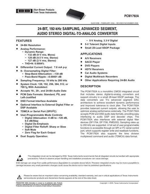
24-Bit, 192-kHz Sampling, Advanced Segment, Audio Stereo DAC ...
24-Bit, 192-kHz Sampling, Advanced Segment, Audio Stereo DAC ...
24-Bit, 192-kHz Sampling, Advanced Segment, Audio Stereo DAC ...

You also want an ePaper? Increase the reach of your titles
YUMPU automatically turns print PDFs into web optimized ePapers that Google loves.
FEATURES<br />
<br />
<br />
<br />
SLES105B − FEBRUARY 2004 − REVISED NOVEMBER 2006<br />
<br />
<br />
<strong>24</strong>-<strong>Bit</strong> Resolution<br />
Analog Performance:<br />
− Dynamic Range:<br />
− 132 dB (9 V rms, Mono)<br />
− 129 dB (4.5 V rms, <strong>Stereo</strong>)<br />
− 127 dB (2 V rms, <strong>Stereo</strong>)<br />
− THD+N: 0.0004%<br />
Differential Current Output: 7.8 mA p-p<br />
8× Oversampling Digital Filter:<br />
− Stop-Band Attenuation: –130 dB<br />
− Pass-Band Ripple: ±0.00001 dB<br />
<strong>Sampling</strong> Frequency: 10 <strong>kHz</strong> to 200 <strong>kHz</strong><br />
System Clock: 128, <strong>192</strong>, 256, 384, 512, or<br />
768 f S With Autodetect<br />
Accepts 16-, 20-, and <strong>24</strong>-<strong>Bit</strong> <strong>Audio</strong> Data<br />
PCM Data Formats: Standard, I 2S, and<br />
Left-Justified<br />
DSD Format Interface Available<br />
Optional Interface to External Digital Filter or<br />
DSP Available<br />
TDMCA or Serial Port (SPI/I 2C)<br />
User-Programmable Mode Controls:<br />
− Digital Attenuation: 0 dB to –120 dB,<br />
0.5 dB/Step<br />
− Digital De-Emphasis<br />
− Digital Filter Rolloff: Sharp or Slow<br />
− Soft Mute<br />
− Zero Flag for Each Output<br />
Dual Supply Operation:<br />
− 5-V Analog, 3.3-V Digital<br />
5-V Tolerant Digital Inputs<br />
Small 28-Lead SSOP Package<br />
APPLICATIONS<br />
A/V Receivers<br />
SACD Player<br />
DVD Players<br />
HDTV Receivers<br />
Car <strong>Audio</strong> Systems<br />
Digital Multitrack Recorders<br />
Other Applications Requiring <strong>24</strong>-<strong>Bit</strong> <strong>Audio</strong><br />
DESCRIPTION<br />
The PCM1792A is a monolithic CMOS integrated circuit<br />
that includes stereo digital-to-analog converters and<br />
support circuitry in a small 28-lead SSOP package. The<br />
data converters use TI’s advanced segment <strong>DAC</strong><br />
architecture to achieve excellent dynamic performance<br />
and improved tolerance to clock jitter. The PCM1792A<br />
provides balanced current outputs, allowing the user to<br />
optimize analog performance externally. The PCM1792A<br />
accepts PCM and DSD audio data formats, providing easy<br />
interfacing to audio DSP and decoder chips. The<br />
PCM1792A also interfaces with external digital filter<br />
devices (DF1704, DF1706, PMD200). <strong>Sampling</strong> rates up<br />
to 200 <strong>kHz</strong> are supported. A full set of user-programmable<br />
functions is accessible through an SPI or I 2 C serial control<br />
port, which supports register write and readback functions.<br />
The PCM1792A also supports the time division<br />
multiplexed command and audio (TDMCA) data format.<br />
This integrated circuit can be damaged by ESD. Texas Instruments recommends that all integrated circuits be handled with appropriate<br />
precautions. Failure to observe proper handling and installation procedures can cause damage.<br />
ESD damage can range from subtle performance degradation to complete device failure. Precision integrated circuits may be more susceptible to<br />
damage because very small parametric changes could cause the device not to meet its published specifications.<br />
Please be aware that an important notice concerning availability, standard warranty, and use in critical applications of Texas Instruments<br />
semiconductor products and disclaimers thereto appears at the end of this data sheet.<br />
<br />
<br />
<br />
Copyright © 2006, Texas Instruments Incorporated
SLES105B − FEBRUARY 2004 − REVISED NOVEMBER 2006<br />
ORDERING INFORMATION<br />
2<br />
PRODUCT PACKAGE PACKAGE CODE<br />
OPERATION<br />
TEMPERATURE<br />
RANGE<br />
PACKAGE<br />
MARKING<br />
PCM1792ADB 28-lead SSOP 28DB −25°C to 85°C PCM1792A<br />
ABSOLUTE MAXIMUM RATINGS<br />
over operating free-air temperature range unless otherwise noted(1)<br />
ORDERING<br />
NUMBER<br />
www.ti.com<br />
TRANSPORT<br />
MEDIA<br />
PCM1792ADB Tube<br />
PCM1792ADBR Tape and reel<br />
PCM1792A<br />
Supply voltage<br />
VCC1, VCC2L, VCC2R<br />
VDD<br />
−0.3 V to 6.5 V<br />
−0.3 V to 4 V<br />
Supply voltage differences: VCC1, VCC2L and VCC2R ±0.1 V<br />
Ground voltage differences: AGND1, AGND2, AGND3L, AGND3R, and DGND ±0.1 V<br />
Digital input LRCK, DATA, BCK, SCK, MSEL, RST, MS(2), MDI, MC, MDO(2), ZEROL(2), ZEROR(2) –0.3 V to 6.5 V<br />
voltage ZEROL(3), ZEROR(3), MDO(3), MS(3) –0.3 V to (VDD + 0.3 V) < 4 V<br />
Analog input voltage –0.3 V to (VCC + 0.3 V) < 6.5 V<br />
Input current (any pins except supplies) ±10 mA<br />
Ambient temperature under bias –40°C to 125°C<br />
Storage temperature –55°C to 150°C<br />
Junction temperature 150°C<br />
Lead temperature (soldering) 260°C, 5 s<br />
Package temperature (IR reflow, peak) 250°C<br />
(1) Stresses beyond those listed under “absolute maximum ratings” may cause permanent damage to the device. These are stress ratings only, and<br />
functional operation of the device at these or any other conditions beyond those indicated under “recommended operating conditions” is not<br />
implied. Exposure to absolute-maximum-rated conditions for extended periods may affect device reliability.<br />
(2) Input mode or I2C mode.<br />
(3) Output mode except for I2C mode.<br />
ELECTRICAL CHARACTERISTICS<br />
all specifications at TA = 25°C, VCC1 = VCC2L = VCC2R = 5 V, fS = 44.1 <strong>kHz</strong>, system clock = 256 fS, and <strong>24</strong>-bit data unless otherwise noted<br />
PARAMETER TEST CONDITIONS<br />
PCM1792ADB<br />
MIN TYP MAX<br />
RESOLUTION <strong>24</strong> <strong>Bit</strong>s<br />
DATA FORMAT (PCM Mode)<br />
<strong>Audio</strong> data interface format Standard, I2S, left justified<br />
<strong>Audio</strong> data bit length 16-, 20-, <strong>24</strong>-bit selectable<br />
<strong>Audio</strong> data format MSB first, 2s complement<br />
fS <strong>Sampling</strong> frequency 10 200 <strong>kHz</strong><br />
System clock frequency 128, <strong>192</strong>, 256, 384, 512, 768 fS<br />
DATA FORMAT (DSD Mode)<br />
<strong>Audio</strong> data interface format DSD (direct stream digital)<br />
<strong>Audio</strong> data bit length 1 <strong>Bit</strong><br />
fS <strong>Sampling</strong> frequency 2.82<strong>24</strong> MHz<br />
System clock frequency 2.82<strong>24</strong> 11.2896 MHz<br />
DIGITAL INPUT/OUTPUT<br />
Logic family TTL compatible<br />
VIH<br />
VIL<br />
Input logic level<br />
IIH<br />
IIL<br />
Input logic current<br />
VOH<br />
VOL<br />
Output logic level<br />
VIN = VDD<br />
10<br />
VIN = 0 V –10<br />
IOH = −2 mA 2.4<br />
IOL = 2 mA 0.4<br />
2<br />
0.8<br />
UNIT<br />
Vdc<br />
µA<br />
Vdc
www.ti.com<br />
<br />
SLES105B − FEBRUARY 2004 − REVISED NOVEMBER 2006<br />
ELECTRICAL CHARACTERISTICS (Continued)<br />
all specifications at TA = 25°C, VCC1 = VCC2L = VCC2R = 5 V, fS = 44.1 <strong>kHz</strong>, system clock = 256 fS, and <strong>24</strong>-bit data unless otherwise noted<br />
PARAMETER TEST CONDITIONS<br />
DYNAMIC PERFORMANCE (PCM MODE, 2-V RMS OUTPUT) (1)(2)<br />
PCM1792ADB<br />
MIN TYP MAX<br />
fS = 44.1 <strong>kHz</strong> 0.0004% 0.0008%<br />
THD+N at VOUT VOUT = 0 dB<br />
fS = 96 <strong>kHz</strong> 0.0008%<br />
fS = <strong>192</strong> <strong>kHz</strong> 0.0015%<br />
EIAJ, A-weighted, fS = 44.1 <strong>kHz</strong> 123 127<br />
Dynamic range<br />
EIAJ, A-weighted, fS = 96 <strong>kHz</strong> 127 dB<br />
EIAJ, A-weighted, fS = <strong>192</strong> <strong>kHz</strong> 127<br />
EIAJ, A-weighted, fS = 44.1 <strong>kHz</strong> 123 127<br />
Signal-to-noise ratio<br />
EIAJ, A-weighted, fS = 96 <strong>kHz</strong> 127 dB<br />
EIAJ, A-weighted, fS = <strong>192</strong> <strong>kHz</strong> 127<br />
fS = 44.1 <strong>kHz</strong> 120 123<br />
Channel separation<br />
fS = 96 <strong>kHz</strong> 122 dB<br />
fS = <strong>192</strong> <strong>kHz</strong> 120<br />
Level Linearity Error VOUT = −120 dB ±1 dB<br />
DYNAMIC PERFORMANCE (PCM Mode, 4.5-V RMS Output) (1)(3)<br />
fS = 44.1 <strong>kHz</strong> 0.0004%<br />
THD+N at VOUT VOUT = 0 dB<br />
fS = 96 <strong>kHz</strong> 0.0008%<br />
fS = <strong>192</strong> <strong>kHz</strong> 0.0015%<br />
EIAJ, A-weighted, fS = 44.1 <strong>kHz</strong> 129<br />
Dynamic range<br />
EIAJ, A-weighted, fS = 96 <strong>kHz</strong> 129 dB<br />
EIAJ, A-weighted, fS = <strong>192</strong> <strong>kHz</strong> 129<br />
EIAJ, A-weighted, fS = 44.1 <strong>kHz</strong> 129<br />
Signal-to-noise ratio<br />
EIAJ, A-weighted, fS = 96 <strong>kHz</strong> 129 dB<br />
EIAJ, A-weighted, fS = <strong>192</strong> <strong>kHz</strong> 129<br />
fS = 44.1 <strong>kHz</strong> 1<strong>24</strong><br />
Channel separation<br />
fS = 96 <strong>kHz</strong> 123 dB<br />
DYNAMIC PERFORMANCE (MONO MODE) (1)(3)<br />
fS = <strong>192</strong> <strong>kHz</strong> 121<br />
fS = 44.1 <strong>kHz</strong> 0.0004%<br />
THD+N at VOUT VOUT = 0 dB<br />
fS = 96 <strong>kHz</strong> 0.0008%<br />
fS = <strong>192</strong> <strong>kHz</strong> 0.0015%<br />
EIAJ, A-weighted, fS = 44.1 <strong>kHz</strong> 132<br />
Dynamic range<br />
EIAJ, A-weighted, fS = 96 <strong>kHz</strong> 132 dB<br />
EIAJ, A-weighted, fS = <strong>192</strong> <strong>kHz</strong> 132<br />
EIAJ, A-weighted, fS = 44.1 <strong>kHz</strong> 132<br />
Signal-to-noise ratio<br />
EIAJ, A-weighted, fS = 96 <strong>kHz</strong> 132 dB<br />
EIAJ, A-weighted, fS = <strong>192</strong> <strong>kHz</strong> 132<br />
(1) Filter condition:<br />
THD+N: 20-Hz HPF, 20-<strong>kHz</strong> apogee LPF<br />
Dynamic range: 20-Hz HPF, 20-<strong>kHz</strong> AES17 LPF, A-weighted<br />
Signal-to-noise ratio: 20-Hz HPF, 20-<strong>kHz</strong> AES17 LPF, A-weighted<br />
Channel separation: 20-Hz HPF, 20-<strong>kHz</strong> AES17 LPF<br />
Analog performance specifications are measured using the System Two Cascade audio measurement system by <strong>Audio</strong> Precision in the<br />
averaging mode.<br />
(2) Dynamic performance and dc accuracy are specified at the output of the postamplifier as shown in Figure 36.<br />
(3) Dynamic performance and dc accuracy are specified at the output of the postamplifier as shown in Figure 37.<br />
<strong>Audio</strong> Precision and System Two are trademarks of <strong>Audio</strong> Precision, Inc.<br />
Other trademarks are the property of their respective owners.<br />
UNIT<br />
3
SLES105B − FEBRUARY 2004 − REVISED NOVEMBER 2006<br />
4<br />
www.ti.com<br />
ELECTRICAL CHARACTERISTICS (Continued)<br />
all specifications at TA = 25°C, VCC1 = VCC2L = VCC2R = 5 V, fS = 44.1 <strong>kHz</strong>, system clock = 256 fS, and <strong>24</strong>-bit data unless otherwise noted<br />
PARAMETER TEST CONDITIONS<br />
DSD MODE DYNAMIC PERFORMANCE (1) (2) (44.1 <strong>kHz</strong>, 64 fS)<br />
PCM1792ADB<br />
MIN TYP MAX<br />
THD+N at FS 4.5 V rms 0.0005%<br />
Dynamic range –60 dB, EIAJ, A-weighted 128 dB<br />
Signal-to-noise ratio EIAJ, A-weighted 128 dB<br />
ANALOG OUTPUT<br />
Gain error –6 ±2 6 % of FSR<br />
Gain mismatch, channel-to-channel –3 ±0.5 3 % of FSR<br />
Bipolar zero error At BPZ –2 ±0.5 2 % of FSR<br />
Output current Full scale (0 dB) 7.8 mA p-p<br />
Center current At BPZ –6.2 mA<br />
DIGITAL FILTER PERFORMANCE<br />
De-emphasis error ±0.004 dB<br />
FILTER CHARACTERISTICS–1: SHARP ROLLOFF<br />
Pass band<br />
±0.00001 dB 0.454 fS<br />
–3 dB 0.49 fS<br />
Stop band 0.546 fS<br />
Pass-band ripple ±0.00001 dB<br />
Stop-band attenuation Stop band = 0.546 fS –130 dB<br />
Delay time 55/fS s<br />
FILTER CHARACTERISTICS–2: SLOW ROLLOFF<br />
Pass band<br />
±0.04 dB 0.254 fS<br />
–3 dB 0.46 fS<br />
Stop band 0.732 fS<br />
Pass-band ripple ±0.001 dB<br />
Stop-band attenuation Stop band = 0.732 fS –100 dB<br />
Delay time<br />
(1) Filter condition:<br />
THD+N: 20-Hz HPF, 20-<strong>kHz</strong> apogee LPF<br />
Dynamic range: 20-Hz HPF, 20-<strong>kHz</strong> AES17 LPF, A-weighted<br />
Signal-to-noise ratio: 20-Hz HPF, 20-<strong>kHz</strong> AES17 LPF, A-weighted<br />
Channel separation: 20-Hz HPF, 20-<strong>kHz</strong> AES17 LPF<br />
18/fS s<br />
Analog performance specifications are measured using the System Two Cascade audio measurement system by <strong>Audio</strong> Precision in the averaging<br />
mode.<br />
(2) Dynamic performance and dc accuracy are specified at the output of the postamplifier as shown in Figure 38.<br />
UNIT
www.ti.com<br />
<br />
SLES105B − FEBRUARY 2004 − REVISED NOVEMBER 2006<br />
ELECTRICAL CHARACTERISTICS (Continued)<br />
all specifications at TA = 25°C, VCC1 = VCC2L = VCC2R = 5 V, fS = 44.1 <strong>kHz</strong>, system clock = 256 fS, and <strong>24</strong>-bit data unless otherwise noted<br />
POWER SUPPLY REQUIREMENTS<br />
PARAMETER TEST CONDITIONS<br />
PCM1792ADB<br />
MIN TYP MAX<br />
VDD 3 3.3 3.6 Vdc<br />
VCC1<br />
VCC2L<br />
VCC2R<br />
Voltage range<br />
UNIT<br />
4.75 5 5.25 Vdc<br />
fS = 44.1 <strong>kHz</strong> 12 15<br />
IDD IDD Supply current (1)<br />
(1) fS = 96 <strong>kHz</strong> 23 mA<br />
fS = <strong>192</strong> <strong>kHz</strong> 45<br />
fS = 44.1 <strong>kHz</strong> 33 40<br />
ICC ICC Supply current (1)<br />
(1) fS = 96 <strong>kHz</strong> 35 mA<br />
fS = <strong>192</strong> <strong>kHz</strong> 37<br />
fS = 44.1 <strong>kHz</strong> 205 250<br />
Power dissipation (1)<br />
fS = 96 <strong>kHz</strong> 250 mW<br />
TEMPERATURE RANGE<br />
fS = <strong>192</strong> <strong>kHz</strong> 335<br />
Operation temperature –25 85 °C<br />
θJA Thermal resistance 28-pin SSOP 100 °C/W<br />
(1) Input is BPZ data.<br />
PIN ASSIGNMENTS<br />
ZEROL<br />
ZEROR<br />
MSEL<br />
LRCK<br />
DATA<br />
BCK<br />
SCK<br />
DGND<br />
V DD<br />
MS<br />
MDI<br />
MC<br />
MDO<br />
RST<br />
1<br />
2<br />
3<br />
4<br />
5<br />
6<br />
7<br />
8<br />
9<br />
10<br />
11<br />
12<br />
13<br />
14<br />
PCM1792A<br />
(TOP VIEW)<br />
28<br />
27<br />
26<br />
25<br />
<strong>24</strong><br />
23<br />
22<br />
21<br />
20<br />
19<br />
18<br />
17<br />
16<br />
15<br />
V CC 2L<br />
AGND3L<br />
I OUT L−<br />
I OUT L+<br />
AGND2<br />
V CC 1<br />
V COM L<br />
V COM R<br />
I REF<br />
AGND1<br />
I OUT R−<br />
I OUT R+<br />
AGND3R<br />
V CC 2R<br />
5
SLES105B − FEBRUARY 2004 − REVISED NOVEMBER 2006<br />
6<br />
TERMINAL<br />
NAME PIN<br />
Terminal Functions<br />
I/O DESCRIPTIONS<br />
AGND1 19 − Analog ground (internal bias)<br />
AGND2 <strong>24</strong> − Analog ground (internal bias)<br />
AGND3L 27 − Analog ground (L-channel <strong>DAC</strong>FF)<br />
AGND3R 16 − Analog ground (R-channel <strong>DAC</strong>FF)<br />
BCK 6 I <strong>Bit</strong> clock input(1)<br />
DATA 5 I Serial audio data input for normal operation(1)<br />
DGND 8 − Digital ground<br />
IOUTL+ 25 O L-channel analog current output+<br />
IOUTL– 26 O L-channel analog current output–<br />
IOUTR+ 17 O R-channel analog current output+<br />
IOUTR– 18 O R-channel analog current output–<br />
IREF 20 − Output current reference bias pin<br />
LRCK 4 I Left and right clock (fS) input for normal operation(1)<br />
MC 12 I Mode control clock input(1)<br />
MDI 11 I Mode control data input(1)<br />
MDO 13 I/O Mode control readback data output(3)<br />
MS 10 I/O Mode control chip-select input(2)<br />
MSEL 3 I I2C/SPI select(1)<br />
RST 14 I Reset(1)<br />
SCK 7 I System clock input(1)<br />
VCC1 23 − Analog power supply, 5 V<br />
VCC2L 28 − Analog power supply (L-channel <strong>DAC</strong>FF), 5 V<br />
VCC2R 15 − Analog power supply (R-channel <strong>DAC</strong>FF), 5 V<br />
VCOML 22 − L-channel internal bias decoupling pin<br />
VCOMR 21 − R-channel internal bias decoupling pin<br />
VDD 9 − Digital power supply, 3.3 V<br />
ZEROL 1 I/O Zero flag for L-channel(2)<br />
www.ti.com<br />
ZEROR 2 I/O Zero flag for R-channel(2)<br />
(1) Schmitt-trigger input, 5-V tolerant<br />
(2) Schmitt-trigger input and output. 5-V tolerant input and CMOS output<br />
(3) Schmitt-trigger input and output. 5-V tolerant input. In I2C mode, this pin becomes an open-drain 3-state output; otherwise, this pin is a CMOS<br />
output.
www.ti.com<br />
FUNCTIONAL BLOCK DIAGRAM<br />
LRCK<br />
BCK<br />
DATA<br />
RST<br />
MDO<br />
MDI<br />
MC<br />
MS<br />
MSEL<br />
ZEROL<br />
ZEROR<br />
<strong>Audio</strong><br />
Data Input<br />
I/F<br />
Function<br />
Control<br />
I/F<br />
Zero<br />
Detect<br />
8<br />
Oversampling<br />
Digital<br />
Filter<br />
and<br />
Function<br />
Control<br />
System<br />
Clock<br />
Manager<br />
SCK<br />
<strong>Advanced</strong><br />
<strong>Segment</strong><br />
<strong>DAC</strong><br />
Modulator<br />
DGND<br />
VDD<br />
AGND1<br />
Bias<br />
and<br />
Vref<br />
Current<br />
<strong>Segment</strong><br />
<strong>DAC</strong><br />
Power Supply<br />
AGND2<br />
AGND3L<br />
Current<br />
<strong>Segment</strong><br />
<strong>DAC</strong><br />
AGND3R<br />
<br />
SLES105B − FEBRUARY 2004 − REVISED NOVEMBER 2006<br />
VCC1<br />
VCC2L<br />
IOUTL−<br />
IOUTL+<br />
VCOML<br />
IREF<br />
VCOMR<br />
IOUTR−<br />
IOUTR+<br />
VCC2R<br />
I/V and Filter<br />
I/V and Filter<br />
VOUTL<br />
VOUTR<br />
7
SLES105B − FEBRUARY 2004 − REVISED NOVEMBER 2006<br />
DIGITAL FILTER<br />
Digital Filter Response<br />
Amplitude − dB<br />
Amplitude − dB<br />
8<br />
0<br />
−50<br />
−100<br />
−150<br />
AMPLITUDE<br />
vs<br />
FREQUENCY<br />
−200<br />
0 1 2 3 4<br />
Frequency [× fS]<br />
Figure 1. Frequency Response, Sharp Rolloff<br />
0<br />
−50<br />
−100<br />
−150<br />
AMPLITUDE<br />
vs<br />
FREQUENCY<br />
−200<br />
0 1 2 3 4<br />
Frequency [× fS]<br />
Figure 3. Frequency Response, Slow Rolloff<br />
TYPICAL PERFORMANCE CURVES<br />
Amplitude − dB<br />
0.00002 2<br />
0.00001 1<br />
0<br />
−0.00001 −1<br />
AMPLITUDE<br />
vs<br />
FREQUENCY<br />
www.ti.com<br />
−0.00002 −2<br />
0.0 0.1 0.2 0.3 0.4 0.5<br />
Frequency [× fS]<br />
Amplitude − dB<br />
Figure 2. Pass-Band Ripple, Sharp Rolloff<br />
0<br />
−2<br />
−4<br />
−6<br />
−8<br />
−10<br />
−12<br />
−14<br />
−16<br />
−18<br />
AMPLITUDE<br />
vs<br />
FREQUENCY<br />
−20<br />
0.0 0.1 0.2 0.3 0.4 0.5 0.6<br />
Frequency [× fS]<br />
Figure 4. Transition Characteristics, Slow Rolloff
www.ti.com<br />
De-Emphasis Filter<br />
De-Emphasis Level − dB<br />
De-Emphasis Level − dB<br />
0<br />
−2<br />
−4<br />
−6<br />
−8<br />
DE-EMPHASIS LEVEL<br />
vs<br />
FREQUENCY<br />
−10<br />
0 2 4 6 8 10 12 14<br />
0<br />
−2<br />
−4<br />
−6<br />
−8<br />
f − Frequency − <strong>kHz</strong><br />
Figure 5<br />
DE-EMPHASIS LEVEL<br />
vs<br />
FREQUENCY<br />
f − Frequency − <strong>kHz</strong><br />
Figure 7<br />
fS = 32 <strong>kHz</strong><br />
fS = 44.1 <strong>kHz</strong><br />
−10<br />
0 2 4 6 8 10 12 14 16 18 20<br />
De-Emphasis Error − dB<br />
De-Emphasis Error − dB<br />
20<br />
0.015 15<br />
0.010 10<br />
0.005 5<br />
0<br />
−0.005 −5<br />
−0.010 −10<br />
−0.015 −15<br />
<br />
SLES105B − FEBRUARY 2004 − REVISED NOVEMBER 2006<br />
fS = 32 <strong>kHz</strong><br />
DE-EMPHASIS ERROR<br />
vs<br />
FREQUENCY<br />
−0.020 −20<br />
0 2 4 6 8 10 12 14<br />
0.020 20<br />
0.015 15<br />
0.010 10<br />
0.005 5<br />
0<br />
−0.005 −5<br />
−0.010 −10<br />
−0.015 −15<br />
fS = 44.1 <strong>kHz</strong><br />
f − Frequency − <strong>kHz</strong><br />
Figure 6<br />
DE-EMPHASIS ERROR<br />
vs<br />
FREQUENCY<br />
−0.020 −20<br />
0 2 4 6 8 10 12 14 16 18 20<br />
f − Frequency − <strong>kHz</strong><br />
Figure 8<br />
9
SLES105B − FEBRUARY 2004 − REVISED NOVEMBER 2006<br />
De-Emphasis Filter (Continued)<br />
De-Emphasis Level − dB<br />
10<br />
0<br />
−2<br />
−4<br />
−6<br />
−8<br />
DE-EMPHASIS LEVEL<br />
vs<br />
FREQUENCY<br />
−10<br />
0 2 4 6 8 10 12 14 16 18 20 22<br />
f − Frequency − <strong>kHz</strong><br />
Figure 9<br />
fS = 48 <strong>kHz</strong><br />
De-Emphasis Error − dB<br />
0.020 20<br />
0.015 15<br />
0.010 10<br />
0.005 5<br />
0<br />
−0.005 −5<br />
−0.010 −10<br />
−0.015 −15<br />
fS = 48 <strong>kHz</strong><br />
DE-EMPHASIS ERROR<br />
vs<br />
FREQUENCY<br />
f − Frequency − <strong>kHz</strong><br />
Figure 10<br />
www.ti.com<br />
−0.020 −20<br />
0 2 4 6 8 10 12 14 16 18 20 22
www.ti.com<br />
ANALOG DYNAMIC PERFORMANCE<br />
Supply Voltage Characteristics<br />
THD+N − Total Harmonic Distortion + Noise − %<br />
SNR − Signal-to-Noise Ratio − dB<br />
0.01<br />
0.001<br />
TOTAL HARMONIC DISTORTION + NOISE<br />
vs<br />
SUPPLY VOLTAGE<br />
fS = <strong>192</strong> <strong>kHz</strong><br />
0.0001<br />
4.50 4.75 5.00 5.25 5.50<br />
132<br />
130<br />
128<br />
126<br />
1<strong>24</strong><br />
fS = 48 <strong>kHz</strong><br />
VCC − Supply Voltage − V<br />
Figure 11<br />
fS = 96 <strong>kHz</strong><br />
SIGNAL-to-NOISE RATIO<br />
vs<br />
SUPPLY VOLTAGE<br />
fS = 48 <strong>kHz</strong><br />
fS = 96 <strong>kHz</strong><br />
Figure 13<br />
fS = <strong>192</strong> <strong>kHz</strong><br />
122<br />
4.50 4.75 5.00 5.25 5.50<br />
VCC − Supply Voltage − V<br />
Dynamic Range − dB<br />
Channel Separation − dB<br />
132<br />
130<br />
128<br />
126<br />
1<strong>24</strong><br />
<br />
SLES105B − FEBRUARY 2004 − REVISED NOVEMBER 2006<br />
fS = 96 <strong>kHz</strong><br />
DYNAMIC RANGE<br />
vs<br />
SUPPLY VOLTAGE<br />
fS = <strong>192</strong> <strong>kHz</strong><br />
122<br />
4.50 4.75 5.00 5.25 5.50<br />
130<br />
128<br />
126<br />
1<strong>24</strong><br />
122<br />
VCC − Supply Voltage − V<br />
Figure 12<br />
VCC − Supply Voltage − V<br />
Figure 14<br />
fS = 48 <strong>kHz</strong><br />
CHANNEL SEPARATION<br />
vs<br />
SUPPLY VOLTAGE<br />
fS = <strong>192</strong> <strong>kHz</strong><br />
NOTE: PCM mode, TA = 25°C, VDD = 3.3 V, measurement circuit is Figure 37 (VOUT = 4.5 V rms).<br />
fS = 96 <strong>kHz</strong><br />
fS = 48 <strong>kHz</strong><br />
120<br />
4.50 4.75 5.00 5.25 5.50<br />
11
SLES105B − FEBRUARY 2004 − REVISED NOVEMBER 2006<br />
Temperature Characteristics<br />
THD+N − Total Harmonic Distortion + Noise − %<br />
SNR − Signal-to-Noise Ratio − dB<br />
12<br />
0.01<br />
0.001<br />
TOTAL HARMONIC DISTORTION + NOISE<br />
vs<br />
FREE-AIR TEMPERATURE<br />
fS = <strong>192</strong> <strong>kHz</strong><br />
0.0001<br />
−50 −25 0 25 50 75 100<br />
132<br />
130<br />
128<br />
126<br />
1<strong>24</strong><br />
TA − Free-Air Temperature − °C<br />
Figure 15<br />
fS = 96 <strong>kHz</strong><br />
SIGNAL-to-NOISE RATIO<br />
vs<br />
FREE-AIR TEMPERATURE<br />
fS = 96 <strong>kHz</strong><br />
fS = <strong>192</strong> <strong>kHz</strong><br />
fS = 48 <strong>kHz</strong><br />
fS = 48 <strong>kHz</strong><br />
122<br />
−50 −25 0 25 50 75 100<br />
TA − Free-Air Temperature − °C<br />
Figure 17<br />
NOTE: PCM mode, VDD = 3.3 V, VCC = 5 V, measurement circuit is Figure 37 (VOUT = 4.5 V rms).<br />
Dynamic Range − dB<br />
Channel Separation − dB<br />
132<br />
130<br />
128<br />
126<br />
1<strong>24</strong><br />
DYNAMIC RANGE<br />
vs<br />
FREE-AIR TEMPERATURE<br />
fS = 96 <strong>kHz</strong><br />
fS = 48 <strong>kHz</strong><br />
TA − Free-Air Temperature − °C<br />
Figure 16<br />
fS = <strong>192</strong> <strong>kHz</strong><br />
www.ti.com<br />
122<br />
−50 −25 0 25 50 75 100<br />
130<br />
128<br />
126<br />
1<strong>24</strong><br />
122<br />
CHANNEL SEPARATION<br />
vs<br />
FREE-AIR TEMPERATURE<br />
fS = <strong>192</strong> <strong>kHz</strong><br />
120<br />
−50 −25 0 25 50 75 100<br />
TA − Free-Air Temperature − °C<br />
Figure 18<br />
fS = 96 <strong>kHz</strong><br />
fS = 48 <strong>kHz</strong>
Amplitude − dB<br />
www.ti.com<br />
0<br />
−20<br />
−40<br />
−60<br />
−80<br />
−100<br />
−120<br />
−140<br />
−160<br />
AMPLITUDE<br />
vs<br />
FREQUENCY<br />
−180<br />
0 2 4 6 8 10 12 14 16 18 20<br />
f − Frequency − <strong>kHz</strong><br />
<br />
SLES105B − FEBRUARY 2004 − REVISED NOVEMBER 2006<br />
−160<br />
0 10 20 30 40 50 60 70 80 90 100<br />
f − Frequency − <strong>kHz</strong><br />
Figure 19. −60-dB Output Spectrum, BW = 20 <strong>kHz</strong> Figure 20. −60-dB Output Spectrum, BW = 100 <strong>kHz</strong><br />
NOTE: PCM mode, fS = 48 <strong>kHz</strong>, 32,768 point 8 average, TA = 25°C, VDD = 3.5 V VCC = 5 V, measurement circuit is Figure 37.<br />
THD+N − Total Harmonic Distortion + Noise − %<br />
10<br />
1<br />
0.1<br />
0.01<br />
0.001<br />
Amplitude − dB<br />
0<br />
−20<br />
−40<br />
−60<br />
−80<br />
−100<br />
−120<br />
−140<br />
TOTAL HARMONIC DISTORTION + NOISE<br />
vs<br />
INPUT LEVEL<br />
0.0001<br />
−100 −80 −60 −40 −20 0<br />
Input Level − dBFS<br />
Figure 21. THD+N vs Input Level, PCM Mode<br />
AMPLITUDE<br />
vs<br />
FREQUENCY<br />
NOTE: PCM mode, fS = 48 <strong>kHz</strong>, TA = 25°C, VDD = 3.3 V, VCC = 5 V, measurement circuit is Figure 37.<br />
13
SLES105B − FEBRUARY 2004 − REVISED NOVEMBER 2006<br />
14<br />
Amplitude − dB<br />
0<br />
−20<br />
−40<br />
−60<br />
−80<br />
−100<br />
−120<br />
−140<br />
AMPLITUDE<br />
vs<br />
FREQUENCY<br />
−160<br />
0 2 4 6 8 10 12 14 16 18 20<br />
f − Frequency − <strong>kHz</strong><br />
Figure 22. −60-dB Output Spectrum, DSD Mode<br />
www.ti.com<br />
NOTE: DSD mode (FIR-4), 32,768 point 8 average, TA = 25°C, VDD = 3.3 V, VCC = 5 V, measurement circuit is Figure 38.<br />
Amplitude − dB<br />
−130<br />
−133<br />
−136<br />
−139<br />
−142<br />
−145<br />
−148<br />
−151<br />
−154<br />
−157<br />
AMPLITUDE<br />
vs<br />
FREQUENCY<br />
−160<br />
0 2 4 6 8 10 12 14 16 18 20<br />
f − Frequency − <strong>kHz</strong><br />
Figure 23. −150-dB Output Spectrum, DSD Mono Mode<br />
NOTE: DSD mode (FIR-4), 32,768 point 8 average, TA = 25°C, VDD = 3.3 V, VCC = 5 V, measurement circuit is Figure 38.
www.ti.com<br />
SYSTEM CLOCK AND RESET FUNCTIONS<br />
System Clock Input<br />
<br />
SLES105B − FEBRUARY 2004 − REVISED NOVEMBER 2006<br />
The PCM1792A requires a system clock for operating the digital interpolation filters and advanced segment <strong>DAC</strong><br />
modulators. The system clock is applied at the SCK input (pin 7). The PCM1792A has a system clock detection circuit that<br />
automatically senses if the system clock is operating between 128 fS and 768 fS. Table 1 shows examples of system clock<br />
frequencies for common audio sampling rates. If the oversampling rate of the delta-sigma modulator is selected as 128 fS,<br />
the system clock frequency is over 256 fS.<br />
Figure <strong>24</strong> shows the timing requirements for the system clock input. For optimal performance, it is important to use a clock<br />
source with low phase jitter and noise. One of the Texas Instruments’ PLL1700 family of multiclock generators is an<br />
excellent choice for providing the PCM1792A system clock.<br />
Table 1. System Clock Rates for Common <strong>Audio</strong> <strong>Sampling</strong> Frequencies<br />
SAMPLING FREQUENCY<br />
128 fS<br />
SYSTEM CLOCK FREQUENCY (fSCK) (MHz)<br />
<strong>192</strong> fS 256 fS 384 fS 512 fS 768 fS<br />
32 <strong>kHz</strong> 4.096(1) 6.144(1) 8.<strong>192</strong> 12.288 16.384 <strong>24</strong>.576<br />
44.1 <strong>kHz</strong> 5.6488(1) 8.4672 11.2896 16.9344 22.5792 33.8688<br />
48 <strong>kHz</strong> 6.144(1) 9.216 12.288 18.432 <strong>24</strong>.576 36.864<br />
96 <strong>kHz</strong> 12.288 18.432 <strong>24</strong>.576 36.864 49.152(1) 73.728(1)<br />
<strong>192</strong> <strong>kHz</strong> <strong>24</strong>.576 36.864 49.152(1) 73.728(1) (2) (2)<br />
(1) This system clock rate is not supported in I2C fast mode.<br />
(2) This system clock rate is not supported for the given sampling frequency.<br />
System Clock (SCK)<br />
H<br />
L<br />
t(SCKL)<br />
t(SCKH)<br />
t(SCY)<br />
PARAMETERS MIN MAX UNITS<br />
t(SCY) System clock pulse cycle time 13 ns<br />
t(SCKH) System clock pulse duration, HIGH 0.4 t(SCY) ns<br />
t(SCKL) System clock pulse duration, LOW 0.4 t(SCY) ns<br />
Power-On and External Reset Functions<br />
Figure <strong>24</strong>. System Clock Input Timing<br />
The PCM1792A includes a power-on reset function. Figure 25 shows the operation of this function. With VDD > 2 V, the<br />
power-on reset function is enabled. The initialization sequence requires 10<strong>24</strong> system clocks from the time VDD > 2 V. After<br />
the initialization period, the PCM1792A is set to its default reset state, as described in the MODE CONTROL REGISTERS<br />
section of this data sheet.<br />
The PCM1792A also includes an external reset capability using the RST input (pin 14). This allows an external controller<br />
or master reset circuit to force the PCM1792A to initialize to its default reset state.<br />
Figure 26 shows the external reset operation and timing. The RST pin is set to logic 0 for a minimum of 20 ns. The RST<br />
pin is then set to a logic 1 state, thus starting the initialization sequence, which requires 10<strong>24</strong> system clock periods. The<br />
external reset is especially useful in applications where there is a delay between the PCM1792A power up and system clock<br />
activation.<br />
2 V<br />
0.8 V<br />
15
SLES105B − FEBRUARY 2004 − REVISED NOVEMBER 2006<br />
16<br />
VDD<br />
2.4 V (Max)<br />
2 V (Typ)<br />
1.6 V (Min)<br />
Internal Reset<br />
System Clock<br />
RST (Pin 14)<br />
Internal Reset<br />
System Clock<br />
Reset Reset Removal<br />
10<strong>24</strong> System Clocks<br />
Figure 25. Power-On Reset Timing<br />
t(RST)<br />
Reset Reset Removal<br />
10<strong>24</strong> System Clocks<br />
50 % of VDD<br />
PARAMETERS MIN MAX UNITS<br />
t(RST) Reset pulse duration, LOW 20 ns<br />
Figure 26. External Reset Timing<br />
www.ti.com
www.ti.com<br />
AUDIO DATA INTERFACE<br />
<strong>Audio</strong> Serial Interface<br />
<br />
SLES105B − FEBRUARY 2004 − REVISED NOVEMBER 2006<br />
The audio interface port is a 3-wire serial port. It includes LRCK (pin 4), BCK (pin 6), and DATA (pin 5). BCK is the serial<br />
audio bit clock, and it is used to clock the serial data present on DATA into the serial shift register of the audio interface.<br />
Serial data is clocked into the PCM1792A on the rising edge of BCK. LRCK is the serial audio left/right word clock.<br />
The PCM1792A requires the synchronization of LRCK and system clock, but does not need a specific phase relation<br />
between LRCK and system clock.<br />
If the relationship between LRCK and system clock changes more than ±6 BCK, internal operation is initialized within 1/fS<br />
and analog outputs are forced to the bipolar zero level until resynchronization between LRCK and system clock is<br />
completed.<br />
PCM <strong>Audio</strong> Data Formats and Timing<br />
The PCM1792A supports industry-standard audio data formats, including standard right-justified, I 2 S, and left-justified. The<br />
data formats are shown in Figure 28. Data formats are selected using the format bits, FMT[2:0], in control register 18. The<br />
default data format is <strong>24</strong>-bit I 2 S. All formats require binary 2s complement, MSB-first audio data. Figure 27 shows a detailed<br />
timing diagram for the serial audio interface.<br />
LRCK<br />
BCK<br />
DATA<br />
t(BCH)<br />
t(BCY)<br />
t(DS)<br />
t(BCL)<br />
t(BL)<br />
t(DH)<br />
t(LB)<br />
PARAMETERS MIN MAX UNITS<br />
t(BCY) BCK pulse cycle time 70 ns<br />
t(BCL) BCK pulse duration, LOW 30 ns<br />
t(BCH) BCK pulse duration, HIGH 30 ns<br />
t(BL) BCK rising edge to LRCK edge 10 ns<br />
t(LB) LRCK edge to BCK rising edge 10 ns<br />
t(DS) DATA setup time 10 ns<br />
t(DH) DATA hold time 10 ns<br />
— LRCK clock duty 50% ± 2 bit clocks<br />
Figure 27. Timing of <strong>Audio</strong> Interface<br />
50% of VDD<br />
50% of VDD<br />
50% of VDD<br />
17
SLES105B − FEBRUARY 2004 − REVISED NOVEMBER 2006<br />
(1) Standard Data Format (Right-Justified); L-Channel = HIGH, R-Channel = LOW<br />
18<br />
LRCK<br />
BCK<br />
<strong>Audio</strong> Data Word = 16-<strong>Bit</strong><br />
DATA<br />
<strong>Audio</strong> Data Word = 20-<strong>Bit</strong><br />
DATA<br />
14 15 16 1 2 15 16<br />
18 19 20<br />
<strong>Audio</strong> Data Word = <strong>24</strong>-<strong>Bit</strong><br />
DATA<br />
LRCK<br />
BCK<br />
22 23 <strong>24</strong><br />
<strong>Audio</strong> Data Word = <strong>24</strong>-<strong>Bit</strong><br />
DATA<br />
LRCK<br />
BCK<br />
<strong>Audio</strong> Data Word = 16-<strong>Bit</strong><br />
DATA<br />
<strong>Audio</strong> Data Word = <strong>24</strong>-<strong>Bit</strong><br />
DATA<br />
MSB LSB<br />
MSB LSB<br />
1 2 15 16<br />
1 2 19 20 1 2 19 20<br />
1 2 23 <strong>24</strong> 1 2 23 <strong>24</strong><br />
MSB<br />
MSB LSB<br />
LSB<br />
1 2 23 <strong>24</strong> 1 2 23 <strong>24</strong><br />
1 2 15 16 1 2 15 16<br />
LSB<br />
L-Channel<br />
(2) Left-Justified Data Format; L-Channel = HIGH, R-Channel = LOW<br />
L-Channel<br />
(3) I 2S Data Format; L-Channel = LOW, R-Channel = HIGH<br />
MSB<br />
L-Channel<br />
LSB<br />
1/f S<br />
1/f S<br />
1/f S<br />
R-Channel<br />
R-Channel<br />
R-Channel<br />
www.ti.com<br />
1 2 23 <strong>24</strong> 1 2 23 <strong>24</strong><br />
1 2<br />
MSB<br />
Figure 28. <strong>Audio</strong> Data Input Formats<br />
1<br />
1<br />
2<br />
2
www.ti.com<br />
External Digital Filter Interface and Timing<br />
<br />
SLES105B − FEBRUARY 2004 − REVISED NOVEMBER 2006<br />
The PCM1792A supports an external digital filter interface comprising a 3- or 4-wire synchronous serial port, which allows<br />
the use of an external digital filter. External filters include the Texas Instruments’ DF1704 and DF1706, the Pacific<br />
Microsonics PMD200, or a programmable digital signal processor.<br />
In the external DF mode, LRCK (pin 4), BCK (pin 6) and DATA (pin 5) are defined as WDCK, the word clock; BCK, the bit<br />
clock; and DATA, the monaural data. The external digital filter interface is selected by using the DFTH bit of control register<br />
20, which functions to bypass the internal digital filter of the PCM1792A.<br />
When the DFMS bit of control register 19 is set, the PCM1792A can process stereo data. In this case, ZEROL (pin 1) and<br />
ZEROR (pin 2) are defined as L-channel data and R-channel data, respectively.<br />
Detailed information for the external digital filter interface mode is provided in the APPLICATION FOR EXTERNAL<br />
DIGITAL FILTER INTERFACE section of this data sheet.<br />
Direct Stream Digital (DSD) Format Interface and Timing<br />
The PCM1792A supports the DSD-format interface operation, which includes out-of-band noise filtering using an internal<br />
analog FIR filter. For DSD operation, SCK (pin 7) is redefined as BCK, DATA (pin 5) as DATAL (left channel audio data),<br />
and LRCK (pin 4) as DATAR (right channel audio data). BCK (pin 6) must be forced low in the DSD mode. The DSD-format<br />
interface is activated by setting the DSD bit of control register 20.<br />
Detailed information for the DSD mode is provided in the APPLICATION FOR DSD-FORMAT (DSD MODE) INTERFACE<br />
section of this data sheet.<br />
TDMCA Interface<br />
The PCM1792A supports the time-division-multiplexed command and audio (TDMCA) data format to enable control of and<br />
communication with a number of external devices over a single serial interface.<br />
Detailed information for the TDMCA format is provided in the TDMCA Format section of this data sheet.<br />
19
SLES105B − FEBRUARY 2004 − REVISED NOVEMBER 2006<br />
FUNCTION DESCRIPTIONS<br />
Zero Detect<br />
20<br />
www.ti.com<br />
The PCM1792A has a zero-detect function. When the PCM1792A detects the zero conditions as shown in Table 2, the<br />
PCM1792A sets ZEROL (pin 1) and ZEROR (pin 2) to HIGH.<br />
Table 2. Zero Conditions<br />
MODE DETECTING CONDITION AND TIME<br />
PCM DATA is continuously LOW for 10<strong>24</strong> LRCKs.<br />
External DF Mode DATA is continuously LOW for 10<strong>24</strong> WDCKs.<br />
DSD<br />
Serial Control Interface<br />
DZ0 There are an equal number of 1s and 0s in every 8 bits of DSD<br />
input data for 200 ms.<br />
DZ1 The input data is 1001 0110 continuously for 200 ms.<br />
The PCM1792A supports SPI and I 2 C serial control interfaces that set the mode control registers as shown in Table 4. This<br />
serial control interface is selected by MSEL (pin 3); SPI is activated when MSEL is set to LOW, and I 2 C is activated when<br />
MSEL is set to HIGH.<br />
SPI Interface<br />
The SPI interface is a 4-wire synchronous serial port which operates asynchronously to the serial audio interface and the<br />
system clock (SCK). The serial control interface is used to program and read the on-chip mode registers. The control<br />
interface includes MDO (pin 13), MDI (pin 11), MC (pin 12), and MS (pin 10). MDO is the serial data output, used to read<br />
back the values of the mode registers; MDI is the serial data input, used to program the mode registers; MC is the serial<br />
bit clock, used to shift data in and out of the control port, and MS is the mode control enable, used to enable the internal<br />
mode register access.<br />
Register Read/Write Operation<br />
All read/write operations for the serial control port use 16-bit data words. Figure 29 shows the control data word format.<br />
The most significant bit is the read/write (R/W) bit. For write operations, the R/W bit must be set to 0. For read operations,<br />
the R/W bit must be set to 1. There are seven bits, labeled IDX[6:0], that hold the register index (or address) for the read<br />
and write operations. The least significant eight bits, D[7:0], contain the data to be written to, or the data that was read from,<br />
the register specified by IDX[6:0].<br />
Figure 30 shows the functional timing diagram for writing or reading the serial control port. MS is held at a logic 1 state until<br />
a register needs to be written or read. To start the register write or read cycle, MS is set to logic 0. Sixteen clocks are then<br />
provided on MC, corresponding to the 16 bits of the control data word on MDI and readback data on MDO. After the eighth<br />
clock cycle has completed, the data from the indexed-mode control register appears on MDO during the read operation.<br />
After the sixteenth clock cycle has completed, the data is latched into the indexed-mode control register during the write<br />
operation. To write or read subsequent data, MS must be set to 1 once.
www.ti.com<br />
MSB<br />
Register Index (or Address) Register Data<br />
<br />
SLES105B − FEBRUARY 2004 − REVISED NOVEMBER 2006<br />
R/W IDX6 IDX5 IDX4 IDX3 IDX2 IDX1 IDX0 D7 D6 D5 D4 D3 D2 D1 D0<br />
MS<br />
MC<br />
MDI<br />
MDO<br />
Figure 29. Control Data Word Format for MDI<br />
R/W A6 A5 A4 A3 A2 A1<br />
High Impedance<br />
A0 D7 D6 D5 D4 D3 D2 D1 D0<br />
D7 D6 D5 D4 D3 D2 D1 D0<br />
When Read Mode is Instructed<br />
NOTE: <strong>Bit</strong> 15 is used for selection of write or read. Setting R/W = 0 indicates a write, while R/W = 1 indicates a read. <strong>Bit</strong>s 14−8 are used for the register<br />
address. <strong>Bit</strong>s 7–0 are used for register data.<br />
MS<br />
MC<br />
MDI<br />
MDO<br />
t(MSS)<br />
t(MCH)<br />
t(MCY)<br />
t(MDS)<br />
Figure 30. Serial Control Format<br />
t(MCL)<br />
t(MDH)<br />
LSB<br />
t(MOS)<br />
t(MHH)<br />
t(MSH)<br />
PARAMETER MIN MAX UNITS<br />
t(MCY) MC pulse cycle time 100 ns<br />
t(MCL) MC low-level time 40 ns<br />
t(MCH) MC high-level time 40 ns<br />
t(MHH) MS high-level time 80 ns<br />
t(MSS) MS falling edge to MC rising edge 15 ns<br />
t(MSH) MS hold time(1) 15 ns<br />
t(MDH) MDI hold time 15 ns<br />
t(MDS) MDI setup time 15 ns<br />
t(MOS) MC falling edge to MDO stable 30 ns<br />
(1) MC rising edge for LSB to MS rising edge<br />
Figure 31. Control Interface Timing<br />
LSB<br />
50% of VDD<br />
50% of VDD<br />
50% of VDD<br />
50% of VDD<br />
21
SLES105B − FEBRUARY 2004 − REVISED NOVEMBER 2006<br />
I 2C Interface<br />
22<br />
www.ti.com<br />
The PCM1792A supports the I2C serial bus and the data transmission protocol for standard and fast mode as a slave<br />
device. This protocol is explained in I2C specification 2.0.<br />
In I2C mode, the control terminals are changed as follows.<br />
TERMINAL NAME TDMCA NAME PROPERTY DESCRIPTION<br />
MS ADR0 Input I2C address 0<br />
MDI ADR1 Input I2C address 1<br />
MC SCL Input I2C clock<br />
MDO SDA Input/output I2C data<br />
Slave Address<br />
MSB LSB<br />
1 0 0 1 1 ADR1 ADR0 R/W<br />
The PCM1792A has 7 bits for its own slave address. The first five bits (MSBs) of the slave address are factory preset to<br />
10011. The next two bits of the address byte are the device select bits which can be user-defined by the ADR1 and ADR0<br />
terminals. A maximum of four PCM1792As can be connected on the same bus at one time. Each PCM1792A responds<br />
when it receives its own slave address.<br />
Packet Protocol<br />
A master device must control packet protocol, which consists of start condition, slave address, read/write bit, data if write<br />
or acknowledge if read, and stop condition. The PCM1792A supports only slave receivers and slave transmitters.<br />
SDA<br />
SCL St<br />
Start<br />
Condition<br />
Write Operation<br />
Read Operation<br />
1−7 8 9 1−8 9 1−8 9 9 Sp<br />
Slave Address R/W ACK DATA ACK DATA ACK ACK<br />
R/W: Read Operation if 1; Otherwise, Write Operation<br />
DATA: 8 <strong>Bit</strong>s (Byte)<br />
ACK: Acknowledgement of a Byte if 0<br />
NACK:Not Acknowledgement if 1<br />
Transmitter M M M S M S M S S M<br />
Data Type St Slave Address W ACK DATA ACK DATA ACK ACK Sp<br />
Transmitter M M M S S M S M M M<br />
Data Type St Slave Address R ACK DATA ACK DATA ACK NACK Sp<br />
M: Master Device S: Slave Device<br />
St: Start Condition Sp: Stop Condition W: Write R: Read<br />
Figure 32. Basic I 2C Framework<br />
Stop<br />
Condition
www.ti.com<br />
Write Register<br />
<br />
SLES105B − FEBRUARY 2004 − REVISED NOVEMBER 2006<br />
A master can write to any PCM1792A registers using single or multiple accesses. The master sends a PCM1792A slave<br />
address with a write bit, a register address, and the data. If multiple access is required, the address is that of the starting<br />
register, followed by the data to be transferred. When the data are received properly, the index register is incremented by<br />
1 automatically. When the index register reaches 0x7F, the next value is 0x0. When undefined registers are accessed, the<br />
PCM1792A does not send an acknowledgement. Figure 33 is a diagram of the write operation.<br />
Transmitter M M M S M S M<br />
Data Type St Slave Address W ACK Reg Address ACK Write Data 1<br />
Read Register<br />
M: Master Device S: Slave Device<br />
St: Start Condition ACK: Acknowledge Sp: Stop Condition W: Write<br />
Figure 33. Write Operation<br />
S<br />
ACK<br />
M<br />
Write Data 2<br />
A master can read the PCM1792A register. The value of the register address is stored in an indirect index register in<br />
advance. The master sends a PCM1792A slave address with a read bit after storing the register address. Then the<br />
PCM1792A transfers the data which the index register points to. When the data are transferred during a multiple access,<br />
the index register is incremented by 1 automatically. (When first going into read mode immediately following a write, the<br />
index register is not incremented. The master can read the register that was previously written.) When the index register<br />
reaches 0x7F, the next value is 0x0. The PCM1792A outputs some data when the index register is 0x10 to 0x1F, even if<br />
it is not defined in Table 4. Figure 34 is a diagram of the read operation.<br />
Transmitter M M M S M S M M<br />
Data Type St Slave Address W ACK Reg Address ACK Sr Slave Address<br />
S<br />
ACK<br />
Data<br />
S<br />
ACK<br />
Slave M<br />
M: Master Device S: Slave Device<br />
St: Start Condition Sr: Repeated Start Condition ACK: Acknowledge Sp: Stop Condition NACK: Not Acknowledge<br />
W: Write R: Read<br />
Noise Suppression<br />
Figure 34. Read Operation<br />
The PCM1792A incorporates noise suppression using the system clock (SCK). However, there must be no more than two<br />
noise spikes in 600 ns. The noise suppression works for SCK frequencies between 8 MHz and 40 MHz in fast mode.<br />
However, it works incorrectly in the following conditions.<br />
Case 1:<br />
1. t (SCK) > 120 ns (t (SCK): period of SCK)<br />
2. t (HI) + t (D−HD) < t (SCK) × 5<br />
3. Spike noise exists on the first half of the SCL HIGH pulse.<br />
4. Spike noise exists on the SDA HIGH pulse just before SDA goes LOW.<br />
SCL<br />
SDA<br />
Noise<br />
When these conditions occur at the same time, the data is recognized as LOW.<br />
M<br />
R<br />
ACK<br />
S<br />
ACK<br />
S<br />
NACK<br />
M<br />
Sp<br />
M<br />
Sp<br />
23
SLES105B − FEBRUARY 2004 − REVISED NOVEMBER 2006<br />
Case 2:<br />
1. t( SCK) > 120 ns<br />
2. t (S−HD) or t (RS−HD) < t (SCK) × 5<br />
3. Spike noise exists on both SCL and SDA during the hold time.<br />
<strong>24</strong><br />
SCL<br />
SDA<br />
Noise<br />
When these conditions occur at the same time, the PCM1792A fails to detect a start condition.<br />
Case 3:<br />
1. t (SCK) < 50 ns<br />
2. t (SP) > t (SCK)<br />
3. Spike noise exists on SCL just after SCL goes LOW.<br />
4. Spike noise exists on SDA just before SCL goes LOW.<br />
SCL<br />
SDA<br />
When these conditions occur at the same time, the PCM1792A erroneously detects a start or stop condition.<br />
Noise<br />
www.ti.com
www.ti.com<br />
TIMING DIAGRAM<br />
SDA<br />
SCL<br />
t(BUF)<br />
t(S-HD)<br />
Start<br />
t(D-SU)<br />
t(LOW)<br />
t(SCL-F)<br />
t(SCL-R)<br />
t(HI)<br />
t(D-HD)<br />
Repeated Start<br />
t(RS-SU)<br />
<br />
SLES105B − FEBRUARY 2004 − REVISED NOVEMBER 2006<br />
t(RS-HD)<br />
t(SDA-R)<br />
t(SP)<br />
t(SDA-F)<br />
t(P-SU)<br />
TIMING CHARACTERISTICS<br />
PARAMETER CONDITIONS MIN MAX UNIT<br />
f(SCL) f(SCL)<br />
t(BUF) t(BUF)<br />
t(LOW) t(LOW)<br />
t(HI) t(HI)<br />
SCL clock frequency<br />
Bus free time between stop and start conditions<br />
Low period of the SCL clock<br />
High period of the SCL clock<br />
t(RS-SU) t(RS-SU) Setup time for (repeated) start condition<br />
t(S-HD)<br />
t(RS-HD)<br />
t(D-SU) t(D-SU)<br />
t(D-HD) t(D-HD)<br />
Hold time for (repeated) start condition<br />
Data setup time<br />
Data hold time<br />
t(SCL-R) t(SCL-R) Rise time of SCL signal<br />
Standard 100<br />
Fast 400<br />
Standard 4.7<br />
Fast 1.3<br />
Standard 4.7<br />
Fast 1.3<br />
Stop<br />
<strong>kHz</strong><br />
µs<br />
µs<br />
Standard 4 µs<br />
Fast 600 ns<br />
Standard 4.7 µs<br />
Fast 600 ns<br />
Standard 4 µs<br />
Fast 600 ns<br />
Standard 250<br />
Fast 100<br />
Standard 0 900<br />
Fast 0 900<br />
Standard 20 + 0.1 CB 1000<br />
Fast 20 + 0.1 CB 300<br />
t(SCL-R1) Rise time of SCL signal after a repeated start condition and after an Rise time of SCL signal after a repeated start condition and after an<br />
Standard 20 + 0.1 CB 1000<br />
t(SCL-R1)<br />
acknowledge bit Fast 20 + 0.1 CB 300<br />
t(SCL-F) t(SCL-F) Fall time of SCL signal<br />
t(SDA-R) t(SDA-R) Rise time of SDA signal<br />
t(SDA-F) t(SDA-F) Fall time of SDA signal<br />
t(P-SU) t(P-SU)<br />
Setup time for stop condition<br />
Standard 20 + 0.1 CB 1000<br />
Fast 20 + 0.1 CB 300<br />
Standard 20 + 0.1 CB 1000<br />
Fast 20 + 0.1 CB 300<br />
Standard 20 + 0.1 CB 1000<br />
Fast 20 + 0.1 CB 300<br />
ns<br />
ns<br />
ns<br />
ns<br />
ns<br />
ns<br />
ns<br />
Standard 4 µs<br />
Fast 600 ns<br />
C(B) Capacitive load for SDA and SCL lines 400 pF<br />
t(SP) Pulse duration of suppressed spike Fast 50 ns<br />
VNH VNH<br />
Noise margin at high level for each connected device (including hysteresis)<br />
Standard<br />
Fast 0.2 VDD V<br />
25
SLES105B − FEBRUARY 2004 − REVISED NOVEMBER 2006<br />
MODE CONTROL REGISTERS<br />
User-Programmable Mode Controls<br />
26<br />
www.ti.com<br />
The PCM1792A includes a number of user-programmable functions which are accessed via mode control registers. The<br />
registers are programmed using the serial control interface, which was previously discussed in this data sheet. Table 3 lists<br />
the available mode-control functions, along with their default reset conditions and associated register index.<br />
Table 3. User-Programmable Function Controls<br />
FUNCTION DEFAULT REGISTER BIT PCM DSD<br />
Digital attenuation control<br />
0 dB to –120 dB and mute, 0.5 dB/step<br />
Attenuation load control<br />
Disabled, enabled<br />
Input audio data format selection<br />
16-, 20-, <strong>24</strong>-bit standard (right-justified) format<br />
<strong>24</strong>-bit MSB-first left-justified format<br />
16-/<strong>24</strong>-bit I2S format<br />
<strong>Sampling</strong> rate selection for de-emphasis<br />
Disabled, 44.1 <strong>kHz</strong>, 48 <strong>kHz</strong>, 32 <strong>kHz</strong><br />
0 dB Register 16<br />
Register 17<br />
ATL[7:0] (for L-ch)<br />
ATR[7:0] (for R-ch)<br />
yes<br />
Attenuation disabled Register 18 ATLD yes<br />
DF<br />
BYPASS<br />
<strong>24</strong>-bit I2S format Register 18 FMT[2:0] yes yes<br />
De-emphasis disabled Register 18 DMF[1:0] yes yes(1)<br />
De-emphasis control<br />
Disabled, enabled<br />
De-emphasis disabled Register 18 DME yes<br />
Soft mute control<br />
Mute disabled, enabled<br />
Mute disabled Register 18 MUTE yes<br />
Output phase reversal<br />
Normal, reverse<br />
Normal Register 19 REV yes yes yes<br />
Attenuation speed selection<br />
×1 fS, ×(1/2) fS, ×(1/4) fS, ×(1/8) fS<br />
×1 fS Register 19 ATS[1:0] yes<br />
<strong>DAC</strong> operation control<br />
Enabled, disabled<br />
<strong>DAC</strong> operation enabled Register 19 OPE yes yes yes<br />
<strong>Stereo</strong> DF bypass mode select<br />
Monaural, stereo<br />
Monaural Register 19 DFMS yes<br />
Digital filter rolloff selection<br />
Sharp rolloff, slow rolloff<br />
Sharp rolloff Register 19 FLT yes<br />
Infinite zero mute control<br />
Disabled, enabled<br />
Disabled Register 19 INZD yes yes<br />
System reset control<br />
Reset operation, normal operation<br />
Normal operation Register 20 SRST yes yes yes<br />
DSD interface mode control<br />
DSD enabled, disabled<br />
Disabled Register 20 DSD yes yes<br />
Digital-filter bypass control<br />
DF enabled, DF bypass<br />
DF enabled Register 20 DFTH yes yes<br />
Monaural mode selection<br />
<strong>Stereo</strong>, monaural<br />
<strong>Stereo</strong> Register 20 MONO yes yes yes<br />
Channel selection for monaural mode data<br />
L-channel, R-channel<br />
L-channel Register 20 CHSL yes yes yes<br />
Delta-sigma oversampling rate selection<br />
×64 fS, ×128 fS, ×32 fS<br />
×64 fS Register 20 OS[1:0] yes yes(2) yes<br />
PCM zero output enable Enabled Register 21 PCMZ yes yes<br />
DSD zero output enable Disabled Register 21 DZ[1:0] yes<br />
Function available only for read<br />
Zero detection flag<br />
Not zero, zero detected<br />
Not zero = 0<br />
Zero detected = 1<br />
Register 22 ZFGL (for L-ch)<br />
ZFGR (for R-ch)<br />
Device ID (at TDMCA) — Register 23 ID[4:0] yes<br />
(1) When in DSD mode, DMF[1:0] is defined as DSD filter (analog FIR) performance selection.<br />
(2) When in DSD mode, OS[1:0] is defined as DSD filter (analog FIR) operation rate selection.<br />
yes yes yes
www.ti.com<br />
Register Map<br />
<br />
SLES105B − FEBRUARY 2004 − REVISED NOVEMBER 2006<br />
The mode control register map is shown in Table 4. Registers 16–21 include an R/W bit, which determines whether a<br />
register read (R/W = 1) or write (R/W = 0) operation is performed. Registers 22 and 23 are read-only.<br />
Table 4. Mode Control Register Map<br />
B15 B14 B13 B12 B11 B10 B9 B8 B7 B6 B5 B4 B3 B2 B1 B0<br />
Register 16 R/W 0 0 1 0 0 0 0 ATL7 ATL6 ATL5 ATL4 ATL3 ATL2 ATL1 ATL0<br />
Register 17 R/W 0 0 1 0 0 0 1 ATR7 ATR6 ATR5 ATR4 ATR3 ATR2 ATR1 ATR0<br />
Register 18 R/W 0 0 1 0 0 1 0 ATLD FMT2 FMT1 FMT0 DMF1 DMF0 DME MUTE<br />
Register 19 R/W 0 0 1 0 0 1 1 REV ATS1 ATS0 OPE RSV DFMS FLT INZD<br />
Register 20 R/W 0 0 1 0 1 0 0 RSV SRST DSD DFTH MONO CHSL OS1 OS0<br />
Register 21 R/W 0 0 1 0 1 0 1 RSV RSV RSV RSV RSV DZ1 DZ0 PCMZ<br />
Register 22 R 0 0 1 0 1 1 0 RSV RSV RSV RSV RSV RSV ZFGR ZFGL<br />
Register 23 R 0 0 1 0 1 1 1 RSV RSV RSV ID4 ID3 ID2 ID1 ID0<br />
Register Definitions<br />
B15 B14 B13 B12 B11 B10 B9 B8 B7 B6 B5 B4 B3 B2 B1 B0<br />
Register 16 R/W 0 0 1 0 0 0 0 ATL7 ATL6 ATL5 ATL4 ATL3 ATL2 ATL1 ATL0<br />
Register 17 R/W 0 0 1 0 0 0 1 ATR7 ATR6 ATR5 ATR4 ATR3 ATR2 ATR1 ATR0<br />
R/W: Read/Write Mode Select<br />
When R/W = 0, a write operation is performed.<br />
When R/W = 1, a read operation is performed.<br />
Default value: 0<br />
ATx[7:0]: Digital Attenuation Level Setting<br />
These bits are available for read and write.<br />
Default value: 1111 1111b<br />
Each <strong>DAC</strong> output has a digital attenuator associated with it. The attenuator can be set from 0 dB to –120 dB, in 0.5-dB steps.<br />
Alternatively, the attenuator can be set to infinite attenuation (or mute).<br />
The attenuation data for each channel can be set individually. However, the data load control (the ATLD bit of control register<br />
18) is common to both attenuators. ATLD must be set to 1 in order to change an attenuator setting. The attenuation level<br />
can be set using the following formula:<br />
Attenuation level (dB) = 0.5 dB • (ATx[7:0] DEC – 255)<br />
where: ATx[7:0]DEC = 0 through 255<br />
For ATx[7:0]DEC = 0 through 14, the attenuator is set to infinite attenuation. The following table shows attenuation levels<br />
for various settings:<br />
ATx[7:0] Decimal Value Attenuation Level Setting<br />
1111 1111b 255 0 dB, no attenuation (default)<br />
1111 1110b 254 –0.5 dB<br />
1111 1101b 253 –1.0 dB<br />
<br />
0001 0000b 16 –119.5 dB<br />
0000 1111b 15 –120.0 dB<br />
0000 1110b 14 Mute<br />
<br />
0000 0000b 0 Mute<br />
27
SLES105B − FEBRUARY 2004 − REVISED NOVEMBER 2006<br />
28<br />
www.ti.com<br />
B15 B14 B13 B12 B11 B10 B9 B8 B7 B6 B5 B4 B3 B2 B1 B0<br />
Register 18 R/W 0 0 1 0 0 1 0 ATLD FMT2 FMT1 FMT0 DMF1 DMF0 DME MUTE<br />
R/W: Read/Write Mode Select<br />
When R/W = 0, a write operation is performed.<br />
When R/W = 1, a read operation is performed.<br />
Default value: 0<br />
ATLD: Attenuation Load Control<br />
This bit is available for read and write.<br />
Default value: 0<br />
ATLD = 0 Attenuation control disabled (default)<br />
ATLD = 1 Attenuation control enabled<br />
The ATLD bit is used to enable loading of the attenuation data contained in registers 16 and 17. When ATLD = 0, the<br />
attenuation settings remain at the previously programmed levels, ignoring new data loaded from registers 16 and 17. When<br />
ATLD = 1, attenuation data written to registers 16 and 17 is loaded normally.<br />
FMT[2:0]: <strong>Audio</strong> Interface Data Format<br />
These bits are available for read and write.<br />
Default value: 101<br />
For the external digital filter interface mode (DFTH mode), this register is operated as shown in the Application for<br />
Interfacing With an External Digital Filter section of this data sheet.<br />
FMT[2:0] <strong>Audio</strong> Data Format Selection<br />
000 16-bit standard, right-justified format data<br />
001 20-bit standard, right-justified format data<br />
010 <strong>24</strong>-bit standard, right-justified format data<br />
011 <strong>24</strong>-bit MSB-first, left-justified format data<br />
100 16-bit I 2S format data<br />
101 <strong>24</strong>-bit I 2S format data (default)<br />
110 Reserved<br />
111 Reserved<br />
The FMT[2:0] bits are used to select the data format for the serial audio interface.<br />
DMF[1:0]: <strong>Sampling</strong> Frequency Selection for the De-Emphasis Function<br />
These bits are available for read and write.<br />
Default value: 00<br />
DMF[1:0] De-Emphasis <strong>Sampling</strong> Frequency Selection<br />
00 Disabled (default)<br />
01 48 <strong>kHz</strong><br />
10 44.1 <strong>kHz</strong><br />
11 32 <strong>kHz</strong><br />
The DMF[1:0] bits are used to select the sampling frequency used by the digital de-emphasis function when it is enabled<br />
by setting the DME bit. The de-emphasis curves are shown in the TYPICAL PERFORMANCE CURVES section of this<br />
data sheet.<br />
For the DSD mode, analog FIR filter performance can be selected using this register. Filter response plots are shown in<br />
the TYPICAL PERFORMANCE CURVES section of this data sheet. A register map is shown in the Configuration for the<br />
DSD Interface Mode section of this data sheet.
www.ti.com<br />
DME: Digital De-Emphasis Control<br />
This bit is available for read and write.<br />
Default value: 0<br />
DME = 0 De-emphasis disabled (default)<br />
DME = 1 De-emphasis enabled<br />
The DME bit is used to enable or disable the de-emphasis function for both channels.<br />
MUTE: Soft Mute Control<br />
This bit is available for read and write.<br />
Default value: 0<br />
MUTE = 0 MUTE disabled (default)<br />
MUTE = 1 MUTE enabled<br />
<br />
SLES105B − FEBRUARY 2004 − REVISED NOVEMBER 2006<br />
The MUTE bit is used to enable or disable the soft mute function for both channels.<br />
Soft mute is operated as a 256-step attenuator. The speed for each step to –∞ dB (mute) is determined by the attenuation<br />
rate selected in the ATS register.<br />
B15 B14 B13 B12 B11 B10 B9 B8 B7 B6 B5 B4 B3 B2 B1 B0<br />
Register 19 R/W 0 0 1 0 0 1 1 REV ATS1 ATS0 OPE RSV DFMS FLT INZD<br />
R/W: Read/Write Mode Select<br />
When R/W = 0, a write operation is performed.<br />
When R/W = 1, a read operation is performed.<br />
Default value: 0<br />
REV: Output Phase Reversal<br />
This bit is available for read and write.<br />
Default value: 0<br />
REV = 0 Normal output (default)<br />
REV = 1 Inverted output<br />
The REV bit is used to invert the output phase for both channels.<br />
ATS[1:0]: Attenuation Rate Select<br />
These bits are available for read and write.<br />
Default value: 00<br />
ATS[1:0] Attenuation Rate Selection<br />
00 LRCK/1 (default)<br />
01 LRCK/2<br />
10 LRCK/4<br />
11 LRCK/8<br />
The ATS[1:0] bits are used to select the rate at which the attenuator is decremented/incremented during level transitions.<br />
29
SLES105B − FEBRUARY 2004 − REVISED NOVEMBER 2006<br />
OPE: <strong>DAC</strong> Operation Control<br />
This bit is available for read and write.<br />
Default value: 0<br />
30<br />
OPE = 0 <strong>DAC</strong> operation enabled (default)<br />
OPE = 1 <strong>DAC</strong> operation disabled<br />
www.ti.com<br />
The OPE bit is used to enable or disable the analog output for both channels. Disabling the analog outputs forces them<br />
to the bipolar zero level (BPZ) even if digital audio data is present on the input.<br />
DFMS: <strong>Stereo</strong> DF Bypass Mode Select<br />
This bit is available for read and write.<br />
Default value: 0<br />
DFMS = 0 Monaural (default)<br />
DFMS = 1 <strong>Stereo</strong> input enabled<br />
The DFMS bit is used to enable stereo operation in DF bypass mode. In the DF bypass mode, when DFMS is set to 0, the<br />
pin for the input data is DATA (pin 5) only, therefore the PCM1792A operates as a monaural <strong>DAC</strong>. When DFMS is set to<br />
1, the PCM1792A can operate as a stereo <strong>DAC</strong> with inputs of L-channel and R-channel data on ZEROL (pin 1) and ZEROR<br />
(pin 2), respectively.<br />
FLT: Digital Filter Rolloff Control<br />
This bit is available for read and write.<br />
Default value: 0<br />
FLT = 0 Sharp rolloff (default)<br />
FLT = 1 Slow rolloff<br />
The FLT bit is used to select the digital filter rolloff characteristic. The filter responses for these selections are shown in the<br />
TYPICAL PERFORMANCE CURVES section of this data sheet.<br />
INZD: Infinite Zero Detect Mute Control<br />
This bit is available for read and write.<br />
Default value: 0<br />
INZD = 0 Infinite zero detect mute disabled (default)<br />
INZD = 1 Infinite zero detect mute enabled<br />
The INZD bit is used to enable or disable the zero detect mute function. Setting INZD to 1 forces muted analog outputs<br />
to hold a bipolar zero level when the PCM1792A detects a zero condition in both channels. The infinite zero detect mute<br />
function is disabled in the DSD mode.<br />
B15 B14 B13 B12 B11 B10 B9 B8 B7 B6 B5 B4 B3 B2 B1 B0<br />
Register 20 R/W 0 0 1 0 1 0 0 RSV SRST DSD DFTH MONO CHSL OS1 OS0<br />
R/W: Read/Write Mode Select<br />
When R/W = 0, a write operation is performed.<br />
When R/W = 1, a read operation is performed.<br />
Default value: 0
www.ti.com<br />
SRST: System Reset Control<br />
This bit is available for write only.<br />
Default value: 0<br />
SRST = 0 Normal operation (default)<br />
SRST = 1 System reset operation (generate one reset pulse)<br />
The SRST bit is used to reset the PCM1792A to the initial system condition.<br />
DSD: DSD Interface Mode Control<br />
This bit is available for read and write.<br />
Default value: 0<br />
DSD = 0 DSD interface mode disabled (default)<br />
DSD = 1 DSD interface mode enabled<br />
The DSD bit is used to enable or disable the DSD interface mode.<br />
DFTH: Digital Filter Bypass (or Through Mode) Control<br />
This bit is available for read and write.<br />
Default value: 0<br />
DFTH = 0 Digital filter enabled (default)<br />
DFTH = 1 Digital filter bypassed for external digital filter<br />
The DFTH bit is used to enable or disable the external digital filter interface mode.<br />
MONO: Monaural Mode Selection<br />
This bit is available for read and write.<br />
Default value: 0<br />
MONO = 0 <strong>Stereo</strong> mode (default)<br />
MONO = 1 Monaural mode<br />
<br />
SLES105B − FEBRUARY 2004 − REVISED NOVEMBER 2006<br />
The MONO function is used to change operation mode from the normal stereo mode to the monaural mode. When the<br />
monaural mode is selected, both <strong>DAC</strong>s operate in a balanced mode for one channel of audio input data. Channel selection<br />
is available for L-channel or R-channel data, determined by the CHSL bit as described immediately following.<br />
CHSL: Channel Selection for Monaural Mode<br />
This bit is available for read and write.<br />
Default value: 0<br />
This bit is available when MONO = 1.<br />
CHSL = 0 L-channel selected (default)<br />
CHSL = 1 R-channel selected<br />
The CHSL bit selects L-channel or R-channel data to be used in monaural mode.<br />
31
SLES105B − FEBRUARY 2004 − REVISED NOVEMBER 2006<br />
OS[1:0]: Delta-Sigma Oversampling Rate Selection<br />
These bits are available for read and write.<br />
Default value: 00<br />
32<br />
OS[1:0] Operation Speed Select<br />
00 64 times fS (default)<br />
01 32 times fS 10 128 times fS 11 Reserved<br />
www.ti.com<br />
The OS bits are used to change the oversampling rate of delta-sigma modulation. Use of this function enables the designer<br />
to stabilize the conditions at the post low-pass filter for different sampling rates. As an application example, programming<br />
to set 128 times in 44.1-<strong>kHz</strong> operation, 64 times in 96-<strong>kHz</strong> operation, and 32 times in <strong>192</strong>-<strong>kHz</strong> operation allows the use<br />
of only a single type (cutoff frequency) of post low-pass filter. The 128 fS oversampling rate is not available at sampling rates<br />
above 100 <strong>kHz</strong>. If the 128-fS oversampling rate is selected, a system clock of more than 256 fS is required.<br />
In DSD mode, these bits are used to select the speed of the bit clock for DSD data coming into the analog FIR filter.<br />
B15 B14 B13 B12 B11 B10 B9 B8 B7 B6 B5 B4 B3 B2 B1 B0<br />
Register 21 R/W 0 0 1 0 1 0 1 RSV RSV RSV RSV RSV DZ1 DZ0 PCMZ<br />
R/W: Read/Write Mode Select<br />
When R/W = 0, a write operation is performed.<br />
When R/W = 1, a read operation is performed.<br />
Default value: 0<br />
DZ[1:0]: DSD Zero Output Enable<br />
These bits are available for read and write.<br />
Default value: 00<br />
DZ[1:0] Zero Output Enable<br />
00 Disabled (default)<br />
01 Even pattern detect<br />
1x 96H pattern detect<br />
The DZ bits are used to enable or disable the output zero flags, and to select the zero pattern in the DSD mode.<br />
PCMZ: PCM Zero Output Enable<br />
These bits are available for read and write.<br />
Default value: 1<br />
PCMZ = 0 PCM zero output disabled<br />
PCMZ = 1 PCM zero output enabled (default)<br />
The PCMZ bit is used to enable or disable the output zero flags in the PCM mode and the external DF mode.<br />
B15 B14 B13 B12 B11 B10 B9 B8 B7 B6 B5 B4 B3 B2 B1 B0<br />
Register 22 R 0 0 1 0 1 1 0 RSV RSV RSV RSV RSV RSV ZFGR ZFGL<br />
R: Read Mode Select<br />
Value is always 1, specifying the readback mode.
www.ti.com<br />
<br />
SLES105B − FEBRUARY 2004 − REVISED NOVEMBER 2006<br />
ZFGx: Zero-Detection Flag<br />
Where x = L or R, corresponding to the <strong>DAC</strong> output channel. These bits are available only for readback.<br />
Default value: 00<br />
ZFGx = 0 Not zero<br />
ZFGx = 1 Zero detected<br />
These bits show zero conditions. Their status is the same as that of the zero flags at ZEROL (pin 1) and ZEROR (pin 2).<br />
See Zero Detect in the FUNCTION DESCRIPTIONS section.<br />
B15 B14 B13 B12 B11 B10 B9 B8 B7 B6 B5 B4 B3 B2 B1 B0<br />
Register 23 R 0 0 1 0 1 1 1 RSV RSV RSV ID4 ID3 ID2 ID1 ID0<br />
R: Read Mode Select<br />
Value is always 1, specifying the readback mode.<br />
ID[4:0]: Device ID<br />
The ID[4:0] bits hold a device ID in the TDMCA mode.<br />
TYPICAL CONNECTION DIAGRAM IN PCM MODE<br />
Controller<br />
PCM<br />
<strong>Audio</strong><br />
Data<br />
Source<br />
0.1 µF<br />
+<br />
10 µF<br />
1<br />
2<br />
3<br />
4<br />
5<br />
6<br />
7<br />
8<br />
9<br />
10<br />
11<br />
12<br />
13<br />
14<br />
3.3 V<br />
ZEROL<br />
ZEROR<br />
MSEL<br />
LRCK<br />
DATA AGND2 <strong>24</strong><br />
BCK<br />
SCK<br />
VCOML<br />
PCM1792A<br />
DGND<br />
VCOMR<br />
VDD<br />
MS<br />
MDI<br />
MC<br />
MDO<br />
RST<br />
VCC2L<br />
AGND3L<br />
IOUTL−<br />
IOUTL+<br />
VCC1<br />
IREF<br />
AGND1<br />
IOUTR−<br />
IOUTR+<br />
AGND3R<br />
VCC2R<br />
28<br />
27<br />
26<br />
25<br />
23<br />
22<br />
21<br />
20<br />
19<br />
18<br />
17<br />
16<br />
15<br />
0.1 µF<br />
+<br />
5 V<br />
+<br />
47 µF<br />
10 kΩ<br />
0.1 µF<br />
+<br />
47 µF<br />
10 µF<br />
10 µF<br />
5 V<br />
10 µF<br />
−<br />
+<br />
−<br />
+<br />
−<br />
+<br />
−<br />
+<br />
Rf<br />
Rf<br />
Rf<br />
Rf<br />
Cf<br />
Cf<br />
Cf<br />
Cf<br />
Differential<br />
to<br />
Single<br />
Converter<br />
With<br />
Low-Pass<br />
Filter<br />
Differential<br />
to<br />
Single<br />
Converter<br />
With<br />
Low-Pass<br />
Filter<br />
Figure 35. Typical Application Circuit for Standard PCM <strong>Audio</strong> Operation<br />
+<br />
+<br />
5 V<br />
VOUT<br />
L-Channel<br />
VOUT<br />
R-Channel<br />
33
SLES105B − FEBRUARY 2004 − REVISED NOVEMBER 2006<br />
APPLICATION CIRCUIT<br />
34<br />
APPLICATION INFORMATION<br />
www.ti.com<br />
The design of the application circuit is important in order to actually realize the high S/N ratio of which the<br />
PCM1792A is capable. This is because noise and distortion that are generated in an application circuit are not<br />
negligible.<br />
In the circuit of Figure 36, the output level is 2 V rms and 127 dB S/N is achieved.<br />
The circuit of Figure 37 can realize the highest performance. In this case the output level is set to 4.5 V rms<br />
and 129 dB S/N is achieved (stereo mode). In monaural mode, if the output of the L-channel and R-channel<br />
is used as a balanced output, 132 dB S/N is achieved (see Figure 39).<br />
Figure 38 shows a circuit for the DSD mode, which is a 4th-order LPF in order to reduce the out-of-band noise.<br />
I/V Section<br />
The current of the PCM1792A on each of the output pins (IOUTL+, IOUTL–, IOUTR+, IOUTR–) is 7.8 mA p-p at<br />
0 dB (full scale). The voltage output level of the I/V converter (Vi) is given by following equation:<br />
Vi = 7.8 mA p-p × Rf (Rf : feedback resistance of I/V converter)<br />
An NE5534 operational amplifier is recommended for the I/V circuit to obtain the specified performance.<br />
Dynamic performance such as the gain bandwidth, settling time, and slew rate of the operational amplifier<br />
affects the audio dynamic performance of the I/V section.<br />
Differential Section<br />
The PCM1792A voltage outputs are followed by differential amplifier stages, which sum the differential signals<br />
for each channel, creating a single-ended I/V op-amp output. In addition, the differential amplifiers provide a<br />
low-pass filter function.<br />
The operational amplifier recommended for the IV circuit is the NE5534, and the operational amplifier<br />
recommended for the differential circuit is the Linear Technology LT1028, because its input noise is low.
IOUT–<br />
IOUT+<br />
www.ti.com<br />
2<br />
3<br />
2<br />
3<br />
VCC<br />
7<br />
–<br />
+<br />
C1<br />
2200 pF<br />
4<br />
VEE<br />
VCC<br />
7<br />
–<br />
+<br />
4<br />
VEE<br />
R1<br />
750 Ω<br />
5<br />
C2<br />
2200 pF<br />
R2<br />
750 Ω<br />
5<br />
C11<br />
0.1 µF<br />
C17<br />
22 pF<br />
8<br />
6<br />
U1<br />
NE5534<br />
C12<br />
0.1 µF<br />
C13<br />
0.1 µF<br />
C18<br />
22 pF<br />
8<br />
6<br />
U2<br />
NE5534<br />
C14<br />
0.1 µF<br />
R3<br />
560 Ω<br />
R4<br />
560 Ω<br />
R5<br />
270 Ω<br />
R6<br />
270 Ω<br />
<br />
SLES105B − FEBRUARY 2004 − REVISED NOVEMBER 2006<br />
C3<br />
2700 pF<br />
C4<br />
2700 pF<br />
7<br />
2<br />
–<br />
5<br />
3<br />
VCC<br />
+<br />
4<br />
VEE<br />
Figure 36. Measurement Circuit for PCM, V OUT = 2 V rms<br />
C15<br />
0.1 µF<br />
C19<br />
33 pF<br />
U3<br />
LT1028<br />
C16<br />
0.1 µF<br />
6<br />
R7<br />
100 Ω<br />
VCC = 15 V<br />
VEE = –15 V<br />
fc = 217 <strong>kHz</strong><br />
35
SLES105B − FEBRUARY 2004 − REVISED NOVEMBER 2006<br />
36<br />
IOUT–<br />
IOUT+<br />
2<br />
3<br />
2<br />
3<br />
VCC<br />
7<br />
–<br />
+<br />
C1<br />
2200 pF<br />
4<br />
VEE<br />
VCC<br />
7<br />
–<br />
+<br />
4<br />
VEE<br />
R1<br />
820 Ω<br />
5<br />
C2<br />
2200 pF<br />
R2<br />
820 Ω<br />
5<br />
C11<br />
0.1 µF<br />
C17<br />
22 pF<br />
8<br />
6<br />
U1<br />
NE5534<br />
C12<br />
0.1 µF<br />
C13<br />
0.1 µF<br />
C18<br />
22 pF<br />
8<br />
6<br />
U2<br />
NE5534<br />
C14<br />
0.1 µF<br />
R3<br />
360 Ω<br />
R4<br />
360 Ω<br />
R5<br />
360 Ω<br />
R6<br />
360 Ω<br />
C3<br />
2700 pF<br />
C4<br />
2700 pF<br />
7<br />
2<br />
–<br />
5<br />
3<br />
VCC<br />
+<br />
4<br />
VEE<br />
Figure 37. Measurement Circuit for PCM, V OUT = 4.5 V rms<br />
C15<br />
0.1 µF<br />
C19<br />
33 pF<br />
U3<br />
LT1028<br />
C16<br />
0.1 µF<br />
6<br />
www.ti.com<br />
R7<br />
100 Ω<br />
VCC = 15 V<br />
VEE = –15 V<br />
fc = 162 <strong>kHz</strong>
IOUT–<br />
IOUT+<br />
www.ti.com<br />
2<br />
3<br />
2<br />
3<br />
VCC<br />
7<br />
–<br />
+<br />
C1<br />
2200 pF<br />
4<br />
VEE<br />
VCC<br />
7<br />
–<br />
+<br />
4<br />
VEE<br />
R1<br />
820 Ω<br />
5<br />
C2<br />
2200 pF<br />
R2<br />
820 Ω<br />
5<br />
C11<br />
0.1 µF<br />
C17<br />
22 pF<br />
8<br />
6<br />
U1<br />
NE5534<br />
C12<br />
0.1 µF<br />
C13<br />
0.1 µF<br />
C18<br />
22 pF<br />
8<br />
6<br />
U2<br />
NE5534<br />
C14<br />
0.1 µF<br />
R3<br />
110 Ω<br />
R4<br />
110 Ω<br />
R8<br />
220 Ω<br />
C3<br />
18000 pF<br />
R9<br />
220 Ω<br />
R5<br />
330 Ω<br />
R6<br />
330 Ω<br />
<br />
SLES105B − FEBRUARY 2004 − REVISED NOVEMBER 2006<br />
C5<br />
10000 pF<br />
R10<br />
68 Ω<br />
C4<br />
47000 pF<br />
R11<br />
68 Ω<br />
C6<br />
10000 pF<br />
Figure 38. Measurement Circuit for DSD<br />
7<br />
2<br />
–<br />
5<br />
3<br />
VCC<br />
+<br />
4<br />
VEE<br />
C15<br />
0.1 µF<br />
C19<br />
33 pF<br />
U3<br />
LT1028<br />
C14<br />
0.1 µF<br />
6<br />
R7<br />
100 Ω<br />
VCC = 15 V<br />
VEE = –15 V<br />
fc = 38 <strong>kHz</strong><br />
37
SLES105B − FEBRUARY 2004 − REVISED NOVEMBER 2006<br />
38<br />
IOUTL– (Pin 26)<br />
IOUTL+ (Pin 25)<br />
IOUTR– (Pin 18)<br />
IOUTR+ (Pin 17)<br />
IOUT–<br />
IOUT+<br />
IOUT–<br />
IOUT+<br />
Figure 37<br />
Circuit<br />
Figure 37<br />
Circuit<br />
OUT+<br />
OUT–<br />
3<br />
2<br />
1<br />
Balanced Out<br />
Figure 39. Measurement Circuit for Monaural Mode<br />
APPLICATION FOR EXTERNAL DIGITAL FILTER INTERFACE<br />
DFMS = 0<br />
DFMS = 1<br />
External Filter Device<br />
WDCK (Word Clock)<br />
External Filter Device<br />
DATA<br />
BCK<br />
SCK<br />
DATA_L<br />
DATA_R<br />
WDCK (Word Clock)<br />
BCK<br />
SCK<br />
1<br />
2<br />
3<br />
4<br />
5<br />
6<br />
7<br />
1<br />
2<br />
3<br />
4<br />
5<br />
6<br />
7<br />
ZEROL<br />
ZEROR<br />
MSEL<br />
LRCK<br />
DATA<br />
BCK<br />
SCK<br />
ZEROL<br />
ZEROR<br />
MSEL<br />
LRCK<br />
DATA<br />
BCK<br />
SCK<br />
PCM1792A<br />
PCM1792A<br />
www.ti.com<br />
Figure 40. Connection Diagram for External DIgital Filter (Internal DF Bypass Mode) Application
www.ti.com<br />
<br />
SLES105B − FEBRUARY 2004 − REVISED NOVEMBER 2006<br />
Application for Interfacing With an External Digital Filter<br />
For some applications, it may be desirable to use an external digital filter to perform the interpolation function,<br />
as it can provide improved stop-band attenuation when compared to the internal digital filter of the PCM1792A.<br />
The PCM1792A supports several external digital filters, including:<br />
Texas Instruments DF1704 and DF1706<br />
Pacific Microsonics PMD200 HDCD filter/decoder IC<br />
Programmable digital signal processors<br />
The external digital filter application mode is accessed by programming the following bits in the corresponding<br />
control register:<br />
DFTH = 1 (register 20)<br />
The pins used to provide the serial interface for the external digital filter are shown in the connection diagram<br />
of Figure 40. The word (WDCK) signal must be operated at 8× or 4× the desired sampling frequency, fS. System Clock (SCK) and Interface Timing<br />
The PCM1792A in an application using an external digital filter requires the synchronization of WDCK and the<br />
system clock. The system clock is phase-free with respect to WDCK. Interface timing among WDCK, BCK,<br />
DATAL, and DATAR is shown in Figure 42.<br />
<strong>Audio</strong> Format<br />
The PCM1792A in the external digital filter interface mode supports right-justified audio formats including 16-bit,<br />
20-bit, and <strong>24</strong>-bit audio data, as shown in Figure 41. The audio format is selected by the FMT[2:0] bits of control<br />
register 18.<br />
WDCK<br />
BCK<br />
<strong>Audio</strong> Data Word = 16-<strong>Bit</strong><br />
DATA<br />
<strong>Audio</strong> Data Word = 20-<strong>Bit</strong><br />
DATA<br />
<strong>Audio</strong> Data Word = <strong>24</strong>-<strong>Bit</strong><br />
DATA<br />
15 16<br />
1/4 f S or 1/8 f S<br />
1 2 3 4 5 6 7 8 9 10 11 12 13 14 15 16<br />
MSB LSB<br />
19 20<br />
1 2 3 4 5 6 7 8 9 10 11 12 13 14 15 16 17 18 19 20<br />
MSB LSB<br />
23 <strong>24</strong><br />
1 2 3 4 5 6 7 8 9 10 11 12 13 14 15 16 17 18 19 20 21 22 23 <strong>24</strong><br />
MSB LSB<br />
Figure 41. <strong>Audio</strong> Data Input Format for External Digital Filter (Internal DF Bypass Mode) Application<br />
39
SLES105B − FEBRUARY 2004 − REVISED NOVEMBER 2006<br />
40<br />
WDCK<br />
(LRCK)<br />
BCK<br />
DATA<br />
t(BCH)<br />
t(BCY)<br />
t(DS)<br />
t(BCL)<br />
t(BL)<br />
t(DH)<br />
t(LB)<br />
PARAMETER MIN MAX UNITS<br />
t(BCY) BCK pulse cycle time 20 ns<br />
t(BCL) BCK pulse duration, LOW 7 ns<br />
t(BCH) BCK pulse duration, HIGH 7 ns<br />
t(BL) BCK rising edge to WDCK falling edge 5 ns<br />
t(LB) WDCK falling edge to BCK rising edge 5 ns<br />
t(DS) DATA setup time 5 ns<br />
t(DH) DATA hold time 5 ns<br />
www.ti.com<br />
50% of VDD<br />
50% of VDD<br />
50% of VDD<br />
Figure 42. <strong>Audio</strong> Interface Timing for External Digital Filter (Internal DF Bypass Mode) Application<br />
Functions Available in the External Digital Filter Mode<br />
The external digital filter mode allows access to the majority of the PCM1792A mode control functions.<br />
The following table shows the register mapping available when the external digital filter mode is selected, along<br />
with descriptions of functions which are modified when using this mode selection.<br />
B15 B14 B13 B12 B11 B10 B9 B8 B7 B6 B5 B4 B3 B2 B1 B0<br />
Register 16 R/W 0 0 1 0 0 0 0 – – – – – – – –<br />
Register 17 R/W 0 0 1 0 0 0 1 – – – – – – – –<br />
Register 18 R/W 0 0 1 0 0 1 0 – FMT2 FMT1 FMT0 – – – –<br />
Register 19 R/W 0 0 1 0 0 1 1 REV – – OPE – DFMS – INZD<br />
Register 20 R/W 0 0 1 0 1 0 0 – SRST 0 1 MONO CHSL OS1 OS0<br />
Register 21 R/W 0 0 1 0 1 0 1 – – – – – – – PCMZ<br />
Register 22 R 0 0 1 0 1 1 0 – – – – – – ZFGR ZFGL<br />
NOTE: 1: <strong>Bit</strong> is required for selection of external digital filter mode.<br />
–: Function is disabled. No operation even if data bit is set<br />
FMT[2:0]: <strong>Audio</strong> Data Format Selection<br />
Default value: 000<br />
FMT[2:0] <strong>Audio</strong> Data Format Select<br />
000 16-bit right-justified format (default)<br />
001 20-bit right-justified format<br />
010 <strong>24</strong>-bit right-justified format<br />
Other N/A
www.ti.com<br />
OS[1:0]: Delta-Sigma Modulator Oversampling Rate Selection<br />
Default value: 00<br />
OS[1:0] Operation Speed Select<br />
00 8 times WDCK (default)<br />
01 4 times WDCK<br />
10 16 times WDCK<br />
11 Reserved<br />
<br />
SLES105B − FEBRUARY 2004 − REVISED NOVEMBER 2006<br />
The effective oversampling rate is determined by the oversampling performed by both the external digital filter<br />
and the delta-sigma modulator. For example, if the external digital filter is 8× oversampling, and the user selects<br />
OS[1:0] = 00, then the delta-sigma modulator oversamples by 8×, resulting in an effective oversampling rate<br />
of 64×. The 16× WDCK oversampling rate is not available above a 100-<strong>kHz</strong> sampling rate. If the oversampling<br />
rate selected is 16× WDCK, the system clock frequency must be over 256 f S.<br />
APPLICATION FOR DSD FORMAT (DSD MODE) INTERFACE<br />
DSD Decoder<br />
DATA_R<br />
DATA_L<br />
<strong>Bit</strong> Clock<br />
1<br />
2<br />
3<br />
4<br />
5<br />
6<br />
7<br />
ZEROL<br />
ZEROR<br />
MSEL<br />
LRCK<br />
DATA<br />
BCK<br />
SCK<br />
Figure 43. Connection Diagram in DSD Mode<br />
PCM1792A<br />
Feature<br />
This mode is used for interfacing directly to a DSD decoder, which is found in Super <strong>Audio</strong> CD (SACD)<br />
applications.<br />
The DSD mode is accessed by programming the following bit in the corresponding control register.<br />
DSD = 1 (register 20)<br />
The DSD mode provides a low-pass filtering function. The filtering is provided using an analog FIR filter<br />
structure. Four FIR responses are available and are selected by the DMF[1:0] bits of control register 18.<br />
The DSD bit must be set before inputting DSD data; otherwise, the PCM1792A erroneously detects the TDMCA<br />
mode, and commands are not accepted through the serial control interface.<br />
Super <strong>Audio</strong> CD is a trademark of Sony Kabushiki Kaisha TA Sony Corporation, Japan.<br />
41
SLES105B − FEBRUARY 2004 − REVISED NOVEMBER 2006<br />
Pin Assignment When Using DSD Format Interface<br />
Several pins are redefined for DSD mode operation. These include:<br />
DATA (pin 5): DSDL as L-channel DSD data input<br />
LRCK (pin 4): DSDR as R-channel DSD data input<br />
SCK (pin 7): DBCK as bit-clock input<br />
BCK (pin 6): Set LOW (N/A)<br />
42<br />
DBCK<br />
DSDL<br />
DSDR<br />
DBCK<br />
DSDL<br />
DSDR<br />
t(BCH)<br />
t = 1/(64 × 44.1 <strong>kHz</strong>)<br />
D0 D1<br />
D2 D3 D4<br />
Figure 44. Normal Data Output Form From DSD Decoder<br />
t(BCY)<br />
t(DS)<br />
t(BCL)<br />
t(DH)<br />
PARAMETER MIN MAX UNITS<br />
t(BCY) DBCK pulse cycle time 85(1) ns<br />
t(BCH) DBCK high-level time 30 ns<br />
t(BCL) DBCK low-level time 30 ns<br />
t(DS) DSDL, DSDR setup time 10 ns<br />
t(DH) DSDL, DSDR hold time 10 ns<br />
(1) 2.82<strong>24</strong> MHz × 4. (2.82<strong>24</strong> MHz = 64 × 44.1 <strong>kHz</strong>. This value is<br />
specified as a sampling rate of DSD.)<br />
Figure 45. Timing for DSD <strong>Audio</strong> Interface<br />
www.ti.com<br />
50% of VDD<br />
50% of VDD
www.ti.com<br />
ANALOG FIR FILTER PERFORMANCE IN DSD MODE<br />
Gain – dB<br />
Gain – dB<br />
0<br />
−1<br />
−2<br />
−3<br />
−4<br />
−5<br />
GAIN<br />
vs<br />
FREQUENCY<br />
−6<br />
0 50 100 150 200<br />
0<br />
−1<br />
−2<br />
−3<br />
−4<br />
−5<br />
f – Frequency – <strong>kHz</strong><br />
Figure 46. DSD Filter-1, Low BW<br />
GAIN<br />
vs<br />
FREQUENCY<br />
−6<br />
0 50 100 150 200<br />
f – Frequency – <strong>kHz</strong><br />
Figure 48. DSD Filter-2, Low BW<br />
(1) This gain is in comparison to PCM 0 dB, when the DSD input signal efficiency is 50%.<br />
Gain – dB<br />
Gain – dB<br />
0<br />
−10<br />
−20<br />
−30<br />
−40<br />
−50<br />
<br />
SLES105B − FEBRUARY 2004 − REVISED NOVEMBER 2006<br />
GAIN<br />
vs<br />
FREQUENCY<br />
fc = 185 <strong>kHz</strong><br />
Gain(1) = –6.6 dB<br />
−60<br />
0 500 1000 1500<br />
f – Frequency – <strong>kHz</strong><br />
Figure 47. DSD Filter-1, High BW<br />
0<br />
−10<br />
−20<br />
−30<br />
−40<br />
−50<br />
GAIN<br />
vs<br />
FREQUENCY<br />
fc = 77 <strong>kHz</strong><br />
Gain(1) = –6 dB<br />
−60<br />
0 500 1000 1500<br />
f – Frequency – <strong>kHz</strong><br />
Figure 49. DSD Filter-2, High BW<br />
All specifications at DBCK = 2.82<strong>24</strong> MHz (44.1 <strong>kHz</strong> × 64 fS), and 50% modulation DSD data input, unless otherwise noted.<br />
43
SLES105B − FEBRUARY 2004 − REVISED NOVEMBER 2006<br />
Gain – dB<br />
Gain – dB<br />
44<br />
0<br />
−1<br />
−2<br />
−3<br />
−4<br />
−5<br />
GAIN<br />
vs<br />
FREQUENCY<br />
−6<br />
0 50 100 150 200<br />
0<br />
−1<br />
−2<br />
−3<br />
−4<br />
−5<br />
f – Frequency – <strong>kHz</strong><br />
Figure 50. DSD Filter-3, Low BW<br />
GAIN<br />
vs<br />
FREQUENCY<br />
−6<br />
0 50 100 150 200<br />
f – Frequency – <strong>kHz</strong><br />
Figure 52. DSD Filter-4, Low BW<br />
(1) This gain is in comparison to PCM 0 dB, when the DSD input signal efficiency is 50%.<br />
Gain – dB<br />
Gain – dB<br />
0<br />
−10<br />
−20<br />
−30<br />
−40<br />
−50<br />
GAIN<br />
vs<br />
FREQUENCY<br />
www.ti.com<br />
fc = 85 <strong>kHz</strong><br />
Gain(1) = –1.5 dB<br />
−60<br />
0 500 1000 1500<br />
f – Frequency – <strong>kHz</strong><br />
Figure 51. DSD Filter-3, High BW<br />
0<br />
−10<br />
−20<br />
−30<br />
−40<br />
−50<br />
GAIN<br />
vs<br />
FREQUENCY<br />
fc = 94 <strong>kHz</strong><br />
Gain(1) = –3.3 dB<br />
−60<br />
0 500 1000 1500<br />
f – Frequency – <strong>kHz</strong><br />
Figure 53. DSD Filter-4, High BW<br />
All specifications at DBCK = 2.82<strong>24</strong> MHz (44.1 <strong>kHz</strong> × 64 fS), and 50% modulation DSD data input, unless otherwise noted.
www.ti.com<br />
DSD MODE CONFIGURATION AND FUNCTION CONTROLS<br />
Configuration for the DSD Interface Mode<br />
DSD = 1 (Register 20, B5)<br />
<br />
SLES105B − FEBRUARY 2004 − REVISED NOVEMBER 2006<br />
B15 B14 B13 B12 B11 B10 B9 B8 B7 B6 B5 B4 B3 B2 B1 B0<br />
Register 16 R/W 0 0 1 0 0 0 0 – – – – – – – –<br />
Register 17 R/W 0 0 1 0 0 0 1 – – – – – – – –<br />
Register 18 R/W 0 0 1 0 0 1 0 – – – – DMF1 DMF0 – –<br />
Register 19 R/W 0 0 1 0 0 1 1 REV – – OPE – – – –<br />
Register 20 R/W 0 0 1 0 1 0 0 – SRST 1 – MONO CHSL OS1 OS0<br />
Register 21 R 0 0 1 0 1 0 1 – – – – – DZ1 DZ0 –<br />
Register 22 R 0 0 1 0 1 1 0 – – – – – – ZFGR ZFGL<br />
NOTE: –: Function is disabled. No operation even if data bit is set<br />
DMF[1:0]: Analog FIR Performance Selection<br />
Default value: 00<br />
DMF[1:0] Analog-FIR Performance Select<br />
00 FIR-1 (default)<br />
01 FIR-2<br />
10 FIR-3<br />
11 FIR-4<br />
Plots for the four analog FIR filter responses are shown in the TYPICAL PERFORMANCE CURVES section<br />
of this data sheet.<br />
OS[1:0]: Analog-FIR Operation-Speed Selection<br />
Default value: 00<br />
OS[1:0] Operation Speed Select<br />
00 fDBCK (default)<br />
01 fDBCK /2<br />
10 Reserved<br />
11 f DBCK/4<br />
The OS bit in the DSD mode is used to select the operating rate of the analog FIR. The OS bits must be set<br />
before setting the DSD bit to1.<br />
TDMCA Format<br />
The PCM1792A supports the time-division-multiplexed command and audio (TDMCA) data format to simplify<br />
the host control serial interface. The TDMCA format is designed not only for the McBSP of TI DSPs but also<br />
for any programmable devices. The TDMCA format can transfer not only audio data but also command data,<br />
so that it can be used together with any kind of device that supports the TDMCA format. The TDMCA frame<br />
consists of command field, extended command field, and some audio data fields. Those audio data are<br />
transported to IN devices (such as a <strong>DAC</strong>) and/or from OUT devices (such as an ADC). The PCM1792A is an<br />
IN device. LRCK and BCK are used with both IN and OUT devices so that the sample frequency of all devices<br />
in a system must be the same. The TDMCA mode supports a maximum of 30 device IDs. The maximum number<br />
of audio channels depends on the BCK frequency.<br />
45
SLES105B − FEBRUARY 2004 − REVISED NOVEMBER 2006<br />
TDMCA Mode Determination<br />
46<br />
www.ti.com<br />
The PCM1792A recognizes the TDMCA mode automatically when it receives an LRCK signal with a pulse<br />
duration of two BCK clocks. If the TDMCA mode operation is not needed, the duty cycle of LRCK must be 50%.<br />
Figure 54 shows the LRCK and BCK timing that determines the TDMCA mode. The PCM1792A enters the<br />
TDMCA mode after two continuous TDMCA frames. Any TDMCA commands can be issued during the next<br />
TDMCA frame after the TDMCA mode is entered.<br />
LRCK<br />
BCK<br />
TDMCA Terminals<br />
Pre-TDMCA Frame<br />
TDMCA Frame<br />
2 BCK<br />
Figure 54. LRCK and BCK Timing of Determination TDMCA Mode<br />
Command<br />
Accept<br />
TDMCA requires six signals, of which four signals are for command and audio data interface, and one pair is<br />
for daisy chaining. Those signals can be shared as in the following table. The DO signal has a 3-state output<br />
so that it can be connected directly to other devices.<br />
TERMINAL<br />
NAME<br />
TDMCA<br />
NAME<br />
PROPERTY DESCRIPTION<br />
LRCK LRCK input TDMCA frame start signal. It must be the same as the sampling frequency.<br />
BCK BCK input<br />
TDMCA clock. Its frequency must be high enough to communicate a TDMCA frame within an LRCK<br />
cycle.<br />
DATA DI input TDMCA command and audio data input signal<br />
MDO DO output TDMCA command data 3-state output signal<br />
MC DCI input TDMCA daisy-chain input signal<br />
MS DCO output TDMCA daisy-chain output signal<br />
Device ID Determination<br />
The TDMCA mode also supports a multichip implementation in one system. This means a host controller (DSP)<br />
can simultaneously support several TDMCA devices, which can be of the same type or different types, including<br />
PCM devices. The PCM devices are categorized as IN device, OUT device, IN/OUT device, and NO device.<br />
The IN device has an input port to get audio data, the OUT device has an output port to supply audio data, the<br />
IN/OUT device has both input and output ports for audio data, and the NO device has no port for audio data<br />
but needs command data from the host. A <strong>DAC</strong> is an IN device, an ADC is an OUT device, a CODEC is an<br />
IN/OUT device, and a PLL is a NO device. The PCM1792A is an IN device. For the host controller to distinguish<br />
the devices, each device is assigned its own device ID by the daisy chain. The devices obtain their own device<br />
IDs automatically by connecting their DCI to the DCO of the preceding device and their DCO to the DCI of the<br />
following device in the daisy chain. The daisy chains are categorized as the IN chain and the OUT chain, which<br />
are completely independent and equivalent. Figure 55 shows an example daisy chain connection. If a system<br />
needs to chain the PCM1792A and a NO device in the same IN or OUT chain, the NO device should be chained<br />
at the back end of the chain because it does not require any audio data. Figure 56 shows an example of TDMCA<br />
system including an IN chain and an OUT chain with a TI DSP. For a device to get its own device ID, the DID<br />
signal must be set to 1 (see the Command Field section for details), and LRCK and BCK must be driven in the<br />
TDMCA mode for all PCM devices which are chained. The device at the top of the chain knows its device ID<br />
is 1 because its DCI is fixed HIGH. Other devices count the BCK pulses and observe their own DCI signal to<br />
determine their position and ID. Figure 57 shows the initialization of each device ID.
www.ti.com<br />
DCI<br />
DCO<br />
IN Device<br />
OUT Device<br />
DCI<br />
OUT Chain<br />
IN Chain<br />
DCO<br />
• • •<br />
• • •<br />
DCI<br />
IN Device<br />
OUT Device<br />
DCI<br />
DCO<br />
DCO<br />
DCIi<br />
DCIo<br />
IN<br />
IN/OUT<br />
Device<br />
OUT<br />
DCOi<br />
DCOo<br />
• • •<br />
DCIi<br />
DCIo<br />
IN<br />
IN/OUT<br />
Device<br />
OUT<br />
<br />
SLES105B − FEBRUARY 2004 − REVISED NOVEMBER 2006<br />
DCOi<br />
DCOo<br />
Figure 55. Daisy-Chain Connection<br />
DCI<br />
DCO<br />
NO Device<br />
NO Device<br />
DCI<br />
DCO<br />
• • •<br />
• • •<br />
DCI<br />
DCO<br />
NO Device<br />
NO Device<br />
DCI<br />
DCO<br />
47
SLES105B − FEBRUARY 2004 − REVISED NOVEMBER 2006<br />
48<br />
TI DSP<br />
FSX<br />
FSR<br />
CLKX<br />
CLKR<br />
DX<br />
DR<br />
LRCK<br />
BCK<br />
DI<br />
DO<br />
LRCK<br />
BCK<br />
DI<br />
IN Device<br />
(PCM1792A)<br />
DCI<br />
DCO<br />
DO Device ID = 2<br />
LRCK<br />
BCK<br />
DI<br />
DO<br />
LRCK<br />
BCK<br />
DI<br />
DO<br />
LRCK<br />
BCK<br />
DI<br />
DO<br />
DCII<br />
IN/OUT DCOI<br />
Device<br />
(DIX1700)<br />
DCIO<br />
DCOO<br />
Device ID = 1<br />
NO Device DCI<br />
DCO<br />
Device ID = 3<br />
•<br />
OUT Device DCI<br />
DCO<br />
Device ID = 2<br />
OUT Device DCI<br />
•<br />
DCO<br />
Device ID = 3<br />
Figure 56. IN Daisy-Chain and OUT Daisy-Chain Connection for a Multichip System<br />
www.ti.com
www.ti.com<br />
Device ID = 1<br />
Device ID = 2<br />
Device ID = 3<br />
•<br />
•<br />
•<br />
Device ID = 30<br />
LRCK<br />
BCK<br />
DI<br />
DCO1<br />
DCO1<br />
DCI2<br />
DCO2<br />
DCI3<br />
•<br />
•<br />
•<br />
DCO29<br />
DCI30<br />
DID<br />
Command Field<br />
58 BCK<br />
Figure 57. Device ID Determination Sequence<br />
<br />
SLES105B − FEBRUARY 2004 − REVISED NOVEMBER 2006<br />
TDMCA Frame<br />
In general, the TDMCA frame consists of the command field, extended command (EMD) field, and audio data<br />
fields. All of them are 32 bits in length, but the lowest byte has no meaning. The MSB is transferred first for each<br />
field. The command field is always transferred as the first packet of the frame. The EMD field is transferred if<br />
the EMD flag of the command field is HIGH. If any EMD packets are transferred, no audio data follows the EMD<br />
packets. This frame is for quick system initialization. All devices of a daisy chain should respond to the command<br />
field and extended command field. The PCM1792A has two audio channels that can be selected by OPE<br />
(register 19). If this OPE bit is not set to HIGH, those audio channels are transferred. Figure 58 shows the<br />
general TDMCA frame. If some <strong>DAC</strong>s are enabled, but corresponding audio data packets are not transferred,<br />
the analog outputs are unpredictable.<br />
LRCK<br />
BCK<br />
[For Initialization]<br />
[For Operation]<br />
Don’t<br />
DI CMD EMD EMD EMD EMD<br />
EMD CMD<br />
32 <strong>Bit</strong>s<br />
DO CMD CMD CMD CMD CMD CMD<br />
DI<br />
CMD Ch1 Ch2 Ch3 Ch4<br />
Ch(n) CMD<br />
DO CMD Ch1 Ch2 Ch3 Ch4<br />
Ch(m)<br />
1/fS<br />
Figure 58. General TDMCA Frame<br />
Care<br />
Don’t<br />
Care<br />
49
SLES105B − FEBRUARY 2004 − REVISED NOVEMBER 2006<br />
50<br />
LRCK<br />
BCK<br />
Don’t<br />
DI CMD Ch1 Ch2 Ch3 Ch4 Ch5 Ch6<br />
CMD<br />
DO<br />
CMD<br />
IN and OUT Channel Orders are Completely Independent<br />
Ch1<br />
1/fS (256 PBCK Clocks)<br />
7 Packets × 32 <strong>Bit</strong>s<br />
Ch2<br />
Figure 59. TDMCA Frame Example of 6-Ch <strong>DAC</strong> and 2-Ch ADC With Command Read<br />
Care<br />
www.ti.com<br />
Command Field<br />
The normal command field is defined as follows. When the DID bit (MSB) is 1, this frame is used only for device<br />
ID determination, and all remaining bits in the field are ignored.<br />
31 30 29 28 <strong>24</strong> 23 22 16 15 8 7 0<br />
command DID EMD DCS device ID R/W register ID data not used<br />
<strong>Bit</strong> 31: Device ID enable flag<br />
The PCM1792A operates to get its own device ID for TDMCA initialization if this bit is HIGH.<br />
<strong>Bit</strong> 30: Extended command enable flag<br />
The EMD packet will be transferred if this bit is HIGH, otherwise skipped. Once this bit is HIGH, this frame does<br />
not contain any audio data. This is for system initialization.<br />
<strong>Bit</strong> 29: Daisy-chain selection flag<br />
HIGH designates OUT-chain devices, LOW designates IN-chain devices. The PCM1792A is an IN device, so<br />
the DCS bit must be set to LOW.<br />
<strong>Bit</strong>s[28:<strong>24</strong>]: Device ID. It is 5 bits length, and it can be defined.<br />
These bits identify the order of a device in the IN or OUT daisy chain. The top of the daisy chain defines device<br />
ID 1 and successive devices are numbered 2, 3, 4, etc. All devices for which the DCI is fixed HIGH are also<br />
defined as ID 1. The maximum device ID is 30 each in the IN and OUT chains. If a device ID of 0x1F is used,<br />
all devices are selected as broadcast when in the write mode. If a device ID of 0x00 is used, no device is<br />
selected.<br />
<strong>Bit</strong> 23: Command Read/Write flag<br />
If this bit is HIGH, the command is a read operation.<br />
<strong>Bit</strong>s[22:16]: Register ID<br />
It is 7 bits in length.<br />
<strong>Bit</strong>s[15:8]: Command data<br />
It is 8 bits in length. Any valid data can be chosen for each register.<br />
<strong>Bit</strong>s[7:0]: Not used<br />
These bits are never transported when a read operation is performed.<br />
Extended command field<br />
The extended command field is the same as the command field, except that it does not have a DID flag.<br />
31 30 29 28 <strong>24</strong> 23 22 16 15 8 7 0<br />
extended command rsvd EMD DCS device ID R/W register ID data not used
www.ti.com<br />
<br />
SLES105B − FEBRUARY 2004 − REVISED NOVEMBER 2006<br />
<strong>Audio</strong> Fields<br />
The audio field is 32 bits in length and the audio data is transferred MSB first, so the other fields must be stuffed<br />
with 0s as shown in the following example.<br />
31 16 12 8 7 4 3 0<br />
audio data MSB <strong>24</strong> bits LSB All 0s<br />
TDMCA Register Requirements<br />
TDMCA mode requires device ID and audio channel information, previously described. The OPE bit in register<br />
19 indicates audio channel availability and register 23 indicates the device ID. Register 23 is used only in the<br />
TDMCA mode. See the mode control register map (Table 4).<br />
Register Write/Read Operation<br />
The command supports register write and read operations. If the command requests to read one register, the<br />
read data is transferred on DO during the data phase of the timing cycle. The DI signal can be retrieved at the<br />
positive edge of BCK, and the DO signal is driven at the negative edge of BCK. DO is activated one BCK cycle<br />
early to compensate for the output delay caused by high impedance. Figure 60 shows the TDMCA write and<br />
read timing.<br />
BCK<br />
DI<br />
DO<br />
DOEN<br />
(Internal)<br />
Register ID Phase Data Phase<br />
Read Mode and Proper Register ID<br />
Write Data Retrieved, if Write Mode<br />
Read Data Driven, if Read Mode<br />
1 BCK Early<br />
Figure 60. TDMCA Write and Read Operation Timing<br />
TDMCA-Mode Operation<br />
DCO specifies the owner of the next audio channel in TDMCA-mode operation. When a device retrieves its own<br />
audio channel data, DCO goes HIGH during the last audio channel period. Figure 61 shows the DCO output<br />
timing in TDMCA-mode operation. The host controller ignores the behavior of DCI and DCO. DCO indicates<br />
the last audio channel of each device. Therefore, DCI means the next audio channel is allocated.<br />
If some devices are skipped due to no active audio channel, the skipped devices must notify the next device<br />
that the DCO will be passed through the next DCI. Figure 62 and Figure 63 show DCO timing with skip<br />
operation. Figure 64 shows the ac timing of the daisy-chain signals.<br />
51
SLES105B − FEBRUARY 2004 − REVISED NOVEMBER 2006<br />
52<br />
DID = 1<br />
DID = 2<br />
DID = 3<br />
DID = 4<br />
LRCK<br />
BCK<br />
DCI1<br />
DCO1<br />
DCI2<br />
DCO2<br />
DCI3<br />
DCO3<br />
DCI4<br />
DCO4<br />
DID = 1<br />
DID = 2<br />
•<br />
•<br />
DID = 8<br />
9 Packets 32 <strong>Bit</strong>s<br />
IN Daisy Chain<br />
1/fS (384 PBCK Clocks)<br />
DI CMD Ch1 Ch2 Ch3 Ch4 Ch5 Ch6 Ch7 Ch8<br />
Don’t Care<br />
LRCK<br />
BCK<br />
DCI<br />
DCO<br />
DCI<br />
DCO<br />
•<br />
DI<br />
DCI<br />
DCO<br />
Figure 61. DCO Output Timing of TDMCA Mode Operation<br />
1/fS (256 PBCK Clocks)<br />
5 Packets × 32 <strong>Bit</strong>s<br />
CMD Ch1 Ch2 Ch15 Ch16 Don’t Care CMD<br />
2 PBCK Delay<br />
14 PBCK Delay<br />
Figure 62. DCO Output Timing With Skip Operation<br />
www.ti.com<br />
CMD
www.ti.com<br />
LRCK<br />
BCK<br />
DI<br />
DCO1<br />
DCO2<br />
•<br />
DID EMD<br />
Command Packet<br />
<br />
SLES105B − FEBRUARY 2004 − REVISED NOVEMBER 2006<br />
Figure 63. DCO Output Timing With Skip Operation (for Command Packet 1)<br />
53
SLES105B − FEBRUARY 2004 − REVISED NOVEMBER 2006<br />
54<br />
LRCK<br />
BCK<br />
DI<br />
DO<br />
DCI<br />
DCO<br />
t(BCY)<br />
t(LB)<br />
t(DS)<br />
t(DS)<br />
t(BL)<br />
t(DH)<br />
t(DH)<br />
www.ti.com<br />
t(DOE)<br />
t(COE)<br />
PARAMETER MIN MAX UNITS<br />
t(BCY) BCK pulse cycle time 20 ns<br />
t(LB) LRCK setup time 0 ns<br />
t(BL) LRCK hold time 3 ns<br />
t(DS) DI setup time 0 ns<br />
t(DH) DI hold time 3 ns<br />
t(DS) DCI setup time 0 ns<br />
t(DH) DCI hold time 3 ns<br />
t(DOE) DO output delay(1) 8 ns<br />
t(COE) DCO output delay(1) 6 ns<br />
(1) Load capacitance is 10 pF.<br />
Figure 64. AC Timing of Daisy-Chain Signals
www.ti.com<br />
THEORY OF OPERATION<br />
Digital Input<br />
<strong>24</strong> <strong>Bit</strong>s<br />
8 fS<br />
Upper<br />
6 <strong>Bit</strong>s<br />
MSB<br />
and<br />
Lower 18 <strong>Bit</strong>s<br />
ICOB<br />
Decoder<br />
3rd-Order<br />
5-Level<br />
Sigma-Delta<br />
0–62<br />
Level<br />
0–4<br />
Level<br />
0–66<br />
<br />
SLES105B − FEBRUARY 2004 − REVISED NOVEMBER 2006<br />
<strong>Advanced</strong><br />
DWA<br />
Figure 65. <strong>Advanced</strong> <strong>Segment</strong>s <strong>DAC</strong><br />
Current<br />
<strong>Segment</strong><br />
<strong>DAC</strong><br />
Analog Output<br />
The PCM1792A uses TI’s advanced segment <strong>DAC</strong> architecture to achieve excellent dynamic performance and<br />
improved tolerance to clock jitter. The PCM1792A provides balanced current outputs.<br />
Digital input data via the digital filter is separated into six upper bits and 18 lower bits. The six upper bits are<br />
converted to inverted complementary offset binary (ICOB) code. The lower 18 bits, associated with the MSB,<br />
are processed by a five-level third-order delta-sigma modulator operated at 64 fS by default. The 1 level of the<br />
modulator is equivalent to the 1 LSB of the ICOB code converter. The data groups processed in the ICOB<br />
converter and third-order delta-sigma modulator are summed together to an up to 66-level digital code, and then<br />
processed by data-weighted averaging (DWA) to reduce the noise produced by element mismatch. The data<br />
of up to 66 levels from the DWA is converted to an analog output in the differential-current segment section.<br />
This architecture has overcome the various drawbacks of conventional multibit processing and also achieves<br />
excellent dynamic performance.<br />
55
SLES105B − FEBRUARY 2004 − REVISED NOVEMBER 2006<br />
56<br />
www.ti.com<br />
Analog output<br />
The following table and Figure 66 show the relationship between the digital input code and analog output.<br />
800000 (–FS) 000000 (BPZ) 7FFFFF (+FS)<br />
IOUTN [mA] –2.3 –6.2 –10.1<br />
IOUTP [mA] –10.1 –6.2 –2.3<br />
VOUTN [V] –1.725 –4.650 –7.575<br />
VOUTP [V] –7.575 –4.650 –1.725<br />
VOUT [V] –2.821 0 2.821<br />
NOTE: VOUTN is the output of U1, VOUTP is the output of U2, and VOUT is the output of U3 in the<br />
measurement circuit of Figure 36.<br />
IO – Output Current – mA<br />
0<br />
−2<br />
−4<br />
−6<br />
−8<br />
−10<br />
−12<br />
OUTPUT CURRENT<br />
vs<br />
INPUT CODE<br />
IOUTN<br />
IOUTP<br />
800000(–FS) 000000(BPZ) 7FFFFF(+FS)<br />
Input Code – Hex<br />
Figure 66. The Relationship Between Digital Input and Analog Output
PACKAGING INFORMATION<br />
Orderable Device Status (1)<br />
Package<br />
Type<br />
Package<br />
Drawing<br />
Pins Package<br />
Qty<br />
PCM1792ADB ACTIVE SSOP DB 28 47 Green (RoHS &<br />
no Sb/Br)<br />
PCM1792ADBG4 ACTIVE SSOP DB 28 47 Green (RoHS &<br />
no Sb/Br)<br />
PCM1792ADBR ACTIVE SSOP DB 28 2000 Green (RoHS &<br />
no Sb/Br)<br />
PCM1792ADBRG4 ACTIVE SSOP DB 28 2000 Green (RoHS &<br />
no Sb/Br)<br />
Eco Plan (2) Lead/Ball Finish MSL Peak Temp (3)<br />
CU NIPDAU Level-1-260C-UNLIM<br />
CU NIPDAU Level-1-260C-UNLIM<br />
CU NIPDAU Level-1-260C-UNLIM<br />
CU NIPDAU Level-1-260C-UNLIM<br />
(1) The marketing status values are defined as follows:<br />
ACTIVE: Product device recommended for new designs.<br />
LIFEBUY: TI has announced that the device will be discontinued, and a lifetime-buy period is in effect.<br />
NRND: Not recommended for new designs. Device is in production to support existing customers, but TI does not recommend using this part in<br />
a new design.<br />
PREVIEW: Device has been announced but is not in production. Samples may or may not be available.<br />
OBSOLETE: TI has discontinued the production of the device.<br />
(2) Eco Plan - The planned eco-friendly classification: Pb-Free (RoHS), Pb-Free (RoHS Exempt), or Green (RoHS & no Sb/Br) - please check<br />
http://www.ti.com/productcontent for the latest availability information and additional product content details.<br />
TBD: The Pb-Free/Green conversion plan has not been defined.<br />
Pb-Free (RoHS): TI's terms "Lead-Free" or "Pb-Free" mean semiconductor products that are compatible with the current RoHS requirements<br />
for all 6 substances, including the requirement that lead not exceed 0.1% by weight in homogeneous materials. Where designed to be soldered<br />
at high temperatures, TI Pb-Free products are suitable for use in specified lead-free processes.<br />
Pb-Free (RoHS Exempt): This component has a RoHS exemption for either 1) lead-based flip-chip solder bumps used between the die and<br />
package, or 2) lead-based die adhesive used between the die and leadframe. The component is otherwise considered Pb-Free (RoHS<br />
compatible) as defined above.<br />
Green (RoHS & no Sb/Br): TI defines "Green" to mean Pb-Free (RoHS compatible), and free of Bromine (Br) and Antimony (Sb) based flame<br />
retardants (Br or Sb do not exceed 0.1% by weight in homogeneous material)<br />
(3) MSL, Peak Temp. -- The Moisture Sensitivity Level rating according to the JEDEC industry standard classifications, and peak solder<br />
temperature.<br />
PACKAGE OPTION ADDENDUM<br />
www.ti.com 7-May-2007<br />
Important Information and Disclaimer:The information provided on this page represents TI's knowledge and belief as of the date that it is<br />
provided. TI bases its knowledge and belief on information provided by third parties, and makes no representation or warranty as to the<br />
accuracy of such information. Efforts are underway to better integrate information from third parties. TI has taken and continues to take<br />
reasonable steps to provide representative and accurate information but may not have conducted destructive testing or chemical analysis on<br />
incoming materials and chemicals. TI and TI suppliers consider certain information to be proprietary, and thus CAS numbers and other limited<br />
information may not be available for release.<br />
In no event shall TI's liability arising out of such information exceed the total purchase price of the TI part(s) at issue in this document sold by TI<br />
to Customer on an annual basis.<br />
Addendum-Page 1
POST OFFICE BOX 655303 • DALLAS, TEXAS 75265<br />
MECHANICAL DATA<br />
MSSO002E – JANUARY 1995 – REVISED DECEMBER 2001<br />
DB (R-PDSO-G**) PLASTIC SMALL-OUTLINE<br />
28 PINS SHOWN<br />
0,38<br />
0,65 0,15 M<br />
0,22<br />
28<br />
1<br />
2,00 MAX<br />
DIM<br />
A<br />
A MAX<br />
A MIN<br />
PINS **<br />
14<br />
6,50<br />
15<br />
14<br />
0,05 MIN<br />
5,60<br />
5,00<br />
8,20<br />
7,40<br />
Seating Plane<br />
<strong>24</strong><br />
8,50<br />
7,90<br />
28<br />
10,50<br />
NOTES: A. All linear dimensions are in millimeters.<br />
B. This drawing is subject to change without notice.<br />
C. Body dimensions do not include mold flash or protrusion not to exceed 0,15.<br />
D. Falls within JEDEC MO-150<br />
5,90<br />
16<br />
6,50<br />
5,90<br />
20<br />
7,50<br />
6,90<br />
0,10<br />
9,90<br />
30<br />
10,50<br />
9,90<br />
0,25<br />
0,09<br />
0°–8°<br />
Gage Plane<br />
38<br />
12,90<br />
12,30<br />
0,25<br />
0,95<br />
0,55<br />
4040065 /E 12/01
IMPORTANT NOTICE<br />
Texas Instruments Incorporated and its subsidiaries (TI) reserve the right to make corrections, modifications, enhancements, improvements,<br />
and other changes to its products and services at any time and to discontinue any product or service without notice. Customers should<br />
obtain the latest relevant information before placing orders and should verify that such information is current and complete. All products are<br />
sold subject to TI’s terms and conditions of sale supplied at the time of order acknowledgment.<br />
TI warrants performance of its hardware products to the specifications applicable at the time of sale in accordance with TI’s standard<br />
warranty. Testing and other quality control techniques are used to the extent TI deems necessary to support this warranty. Except where<br />
mandated by government requirements, testing of all parameters of each product is not necessarily performed.<br />
TI assumes no liability for applications assistance or customer product design. Customers are responsible for their products and<br />
applications using TI components. To minimize the risks associated with customer products and applications, customers should provide<br />
adequate design and operating safeguards.<br />
TI does not warrant or represent that any license, either express or implied, is granted under any TI patent right, copyright, mask work right,<br />
or other TI intellectual property right relating to any combination, machine, or process in which TI products or services are used. Information<br />
published by TI regarding third-party products or services does not constitute a license from TI to use such products or services or a<br />
warranty or endorsement thereof. Use of such information may require a license from a third party under the patents or other intellectual<br />
property of the third party, or a license from TI under the patents or other intellectual property of TI.<br />
Reproduction of TI information in TI data books or data sheets is permissible only if reproduction is without alteration and is accompanied<br />
by all associated warranties, conditions, limitations, and notices. Reproduction of this information with alteration is an unfair and deceptive<br />
business practice. TI is not responsible or liable for such altered documentation. Information of third parties may be subject to additional<br />
restrictions.<br />
Resale of TI products or services with statements different from or beyond the parameters stated by TI for that product or service voids all<br />
express and any implied warranties for the associated TI product or service and is an unfair and deceptive business practice. TI is not<br />
responsible or liable for any such statements.<br />
TI products are not authorized for use in safety-critical applications (such as life support) where a failure of the TI product would reasonably<br />
be expected to cause severe personal injury or death, unless officers of the parties have executed an agreement specifically governing<br />
such use. Buyers represent that they have all necessary expertise in the safety and regulatory ramifications of their applications, and<br />
acknowledge and agree that they are solely responsible for all legal, regulatory and safety-related requirements concerning their products<br />
and any use of TI products in such safety-critical applications, notwithstanding any applications-related information or support that may be<br />
provided by TI. Further, Buyers must fully indemnify TI and its representatives against any damages arising out of the use of TI products in<br />
such safety-critical applications.<br />
TI products are neither designed nor intended for use in military/aerospace applications or environments unless the TI products are<br />
specifically designated by TI as military-grade or "enhanced plastic." Only products designated by TI as military-grade meet military<br />
specifications. Buyers acknowledge and agree that any such use of TI products which TI has not designated as military-grade is solely at<br />
the Buyer's risk, and that they are solely responsible for compliance with all legal and regulatory requirements in connection with such use.<br />
TI products are neither designed nor intended for use in automotive applications or environments unless the specific TI products are<br />
designated by TI as compliant with ISO/TS 16949 requirements. Buyers acknowledge and agree that, if they use any non-designated<br />
products in automotive applications, TI will not be responsible for any failure to meet such requirements.<br />
Following are URLs where you can obtain information on other Texas Instruments products and application solutions:<br />
Products Applications<br />
Amplifiers amplifier.ti.com <strong>Audio</strong> www.ti.com/audio<br />
Data Converters dataconverter.ti.com Automotive www.ti.com/automotive<br />
DLP® Products www.dlp.com Broadband www.ti.com/broadband<br />
DSP dsp.ti.com Digital Control www.ti.com/digitalcontrol<br />
Clocks and Timers www.ti.com/clocks Medical www.ti.com/medical<br />
Interface interface.ti.com Military www.ti.com/military<br />
Logic logic.ti.com Optical Networking www.ti.com/opticalnetwork<br />
Power Mgmt power.ti.com Security www.ti.com/security<br />
Microcontrollers microcontroller.ti.com Telephony www.ti.com/telephony<br />
RFID www.ti-rfid.com Video & Imaging www.ti.com/video<br />
RF/IF and ZigBee® Solutions www.ti.com/lprf Wireless www.ti.com/wireless<br />
Mailing Address: Texas Instruments, Post Office Box 655303, Dallas, Texas 75265<br />
Copyright © 2009, Texas Instruments Incorporated