

Photodiode
Photodiode
Photodiode

Create successful ePaper yourself
Turn your PDF publications into a flip-book with our unique Google optimized e-Paper software.
02/05/09 http://en.wikipedia.org/wiki/<strong>Photodiode</strong> #1<br />
<strong>Photodiode</strong><br />
From Wikipedia, the free encyclopedia<br />
A photodiode is a type of photodetector capable of converting light<br />
into either current or voltage, depending upon the mode of<br />
operation. [1]<br />
<strong>Photodiode</strong>s are similar to regular semiconductor diodes except that<br />
they may be either exposed (to detect vacuum UV or Xrays) or<br />
packaged with a window or optical fibre connection to allow light to<br />
reach the sensitive part of the device. Many diodes designed for use<br />
specifically as a photodiode will also use a PIN junction rather than<br />
the typical PN junction.<br />
Contents<br />
Polarity<br />
1 Polarity<br />
2 Principle of operation<br />
2.1 Photovoltaic mode<br />
2.2 Photoconductive mode<br />
2.3 Other modes of operation<br />
3 Materials<br />
4 Features<br />
5 Applications<br />
5.1 Comparison with photomultipliers<br />
5.2 PN vs. PIN <strong>Photodiode</strong>s<br />
6 <strong>Photodiode</strong> array<br />
7 See also<br />
8 References<br />
9 External links<br />
Some photodiodes will look like the picture to the right, that is, similar to a light emitting diode.<br />
They will have two leads, or wires, coming from the bottom. The shorter end of the two is the<br />
cathode, while the longer end is the anode. See below for a schematic drawing of the anode and<br />
cathode side. Under forward bias, conventional current will pass from the anode to the cathode,<br />
following the arrow in the symbol. Photocurrent flows in the opposite direction.<br />
Principle of operation<br />
A photodiode is a PN junction or PIN structure. When a photon of sufficient energy strikes the<br />
diode, it excites an electron, thereby creating a mobile electron and a positively charged electron<br />
hole. If the absorption occurs in the junction's depletion region, or one diffusion length away from<br />
it, these carriers are swept from the junction by the builtin field of the depletion region. Thus<br />
holes move toward the anode, and electrons toward the cathode, and a<br />
photocurrent is produced.<br />
Photovoltaic mode<br />
When used in zero bias or photovoltaic mode, the flow of photocurrent<br />
out of the device is restricted and a voltage builds up. The diode<br />
becomes forward biased and "dark current" begins to flow across the<br />
junction in the direction opposite to the photocurrent. This mode is<br />
responsible for the photovoltaic effect, which is the basis for solar<br />
cells—in fact, a solar cell is just an array of large area photodiodes.<br />
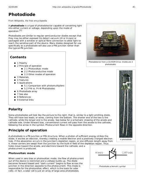
Photodetector from a CDROM Drive. Visible are 3<br />
photodiodes.<br />
A photodiode<br />
<strong>Photodiode</strong> schematic symbol
02/05/09 http://en.wikipedia.org/wiki/<strong>Photodiode</strong> #2<br />
Photoconductive mode<br />
In this mode the diode is often (but not always) reverse biased. This increases the width of the depletion layer, which<br />
decreases the junction's capacitance resulting in faster response times. The reverse bias induces only a small amount<br />
of current (known as saturation or back current) along its direction while the photocurrent remains virtually the same.<br />
The photocurrent is linearly proportional to the illuminance.[1]<br />
(http://hyperphysics.phyastr.gsu.edu/hbase/Electronic/photdet.html)<br />
Although this mode is faster, the photovoltaic mode tends to exhibit less electronic noise. (The leakage current of a<br />
good PIN diode is so low – < 1nA – that the Johnson–Nyquist noise of the load resistance in a typical circuit often<br />
dominates.)<br />
Other modes of operation<br />
Avalanche photodiodes have a similar structure to regular photodiodes, but they are operated with much higher<br />
reverse bias. This allows each photogenerated carrier to be multiplied by avalanche breakdown, resulting in internal<br />
gain within the photodiode, which increases the effective responsivity of the device.<br />
Phototransistors also consist of a photodiode with internal gain. A phototransistor is in essence nothing more than a<br />
bipolar transistor that is encased in a transparent case so that light can reach the basecollector junction. The<br />
electrons that are generated by photons in the basecollector junction are injected into the base, and this photodiode<br />
current is amplified by the transistor's current gain β (or hfe). Note that while phototransistors have a higher<br />
responsivity for light they are not able to detect low levels of light any better than photodiodes. Phototransistors also<br />
have slower response times.<br />
Materials<br />
The material used to make a photodiode is critical to defining its properties, because only photons with sufficient<br />
energy to excite electrons across the material's bandgap will produce significant photocurrents.<br />
Materials commonly used to produce photodiodes include:<br />
Material Wavelength range (nm)<br />
Silicon 190–1100<br />
Germanium 400–1700<br />
Indium gallium arsenide 800–2600<br />
Lead sulfide
02/05/09 http://en.wikipedia.org/wiki/<strong>Photodiode</strong> #3<br />
(NEP) The minimum input optical power to generate photocurrent, equal to the rms noise current in a 1 hertz<br />
bandwidth. The related characteristic detectivity (D) is the inverse of NEP, 1/NEP; and the specific detectivity (<br />
) is the detectivity normalized to the area (A) of the photodetector, . The NEP is roughly the<br />
minimum detectable input power of a photodiode.<br />
When a photodiode is used in an optical communication system, these parameters contribute to the sensitivity of the<br />
optical receiver, which is the minimum input power required for the receiver to achieve a specified bit error ratio.<br />
Applications<br />
PN photodiodes are used in similar applications to other photodetectors, such as photoconductors, chargecoupled<br />
devices, and photomultiplier tubes.<br />
<strong>Photodiode</strong>s are used in consumer electronics devices such as compact disc players, smoke detectors, and the<br />
receivers for remote controls in VCRs and televisions.<br />
In other consumer items such as camera light meters, clock radios (the ones that dim the display when it's dark) and<br />
street lights, photoconductors are often used rather than photodiodes, although in principle either could be used.<br />
<strong>Photodiode</strong>s are often used for accurate measurement of light intensity in science and industry. They generally have a<br />
better, more linear response than photoconductors.<br />
They are also widely used in various medical applications, such as detectors for computed tomography (coupled with<br />
scintillators) or instruments to analyze samples (immunoassay). They are also used in blood gas monitors.<br />
PIN diodes are much faster and more sensitive than ordinary pn junction diodes, and hence are often used for optical<br />
communications and in lighting regulation.<br />
PN photodiodes are not used to measure extremely low light intensities. Instead, if high sensitivity is needed,<br />
avalanche photodiodes, intensified chargecoupled devices or photomultiplier tubes are used for applications such as<br />
astronomy, spectroscopy, night vision equipment and laser rangefinding.<br />
Comparison with photomultipliers<br />
Advantages compared to photomultipliers:<br />
1. Excellent linearity of output current as a function of incident light<br />
2. Spectral response from 190 nm to 1100 nm (silicon), longer wavelengths with other semiconductor materials<br />
3. Low noise<br />
4. Ruggedized to mechanical stress<br />
5. Low cost<br />
6. Compact and light weight<br />
7. Long lifetime<br />
8. High quantum efficiency, typically 80%<br />
9. No high voltage required<br />
Disadvantages compared to photomultipliers:<br />
1. Small area<br />
2. No internal gain (except avalanche photodiodes, but their gain is typically 10²–10³ compared to up to 108 for<br />
the photomultiplier)<br />
3. Much lower overall sensitivity<br />
4. Photon counting only possible with specially designed, usually cooled photodiodes, with special electronic<br />
circuits<br />
5. Response time for many designs is slower<br />
PN vs. PIN <strong>Photodiode</strong>s<br />
1. Due to the intrinsic layer, a PIN photodiode must be reverse biased (Vr). The Vr increases the depletion region<br />
allowing a larger volume for electronhole pair production, and reduces the capacitance thereby increasing the<br />
bandwidth.<br />
2. The Vr also introduces noise current, which reduces the S/N ratio. Therefore, a reverse bias is recommended for<br />
higher bandwidth applications and/or applications where a wide dynamic range is required.<br />
3. A PN photodiode is more suitable for lower light applications because it allows for unbiased operation.
02/05/09 http://en.wikipedia.org/wiki/<strong>Photodiode</strong> #4<br />
<strong>Photodiode</strong> array<br />
Hundreds or thousands (up to 2048) photodiodes of typical sensitive area 0.025mmx1mm each arranged as a<br />
onedimensional array, which can be used as a position sensor. One advantage of photodiode arrays (PDAs) is that<br />
they allow for high speed parallel read out since the driving electronics may not be built in like a traditional CMOS or<br />
CCD sensor.<br />
See also<br />
Electronics<br />
Band gap<br />
Infrared<br />
Optoelectronics<br />
Optoisolator<br />
Semiconductor device<br />
Solar cell<br />
Avalanche photodiode<br />
Transducer<br />
LEDs as <strong>Photodiode</strong> Light Sensors<br />
Light meter<br />
Ambientlight meter<br />
References<br />
This article contains material from the Federal Standard 1037C, which, as a work of the United States Government, is<br />
in the public domain.<br />
1. ^ International Union of Pure and Applied Chemistry. "<strong>Photodiode</strong> (http://goldbook.iupac.org/P04598.html) ". Compendium of Chemical<br />
Terminology Internet edition.<br />
Gowar, John, Optical Communication Systems, 2 ed., PrenticeHall, Hempstead UK, 1993 (ISBN 0136387276)<br />
External links<br />
Technical Information Hamamatsu Photonics<br />
(http://sales.hamamatsu.com/assets/html/ssd/siphotodiode/index.htm)<br />
Using the <strong>Photodiode</strong> to convert the PC to a Light Intensity Logger (http://www.emant.com/324003.page)<br />
Design Fundamentals for Phototransistor Circuits (http://www.fairchildsemi.com/an/AN/AN3005.pdf)<br />
Working principles of photodiodes (http://ecewww.colorado.edu/~bart/book/book/chapter4/ch4_7.htm)<br />
Retrieved from "http://en.wikipedia.org/wiki/<strong>Photodiode</strong>"<br />
Category: Optical diodes<br />
Hidden categories: Articles needing more detailed references | All articles with unsourced statements | Articles with<br />
unsourced statements since January 2008 | Articles with unsourced statements since July 2008 | Wikipedia articles<br />
incorporating text from the Federal Standard 1037C<br />
This page was last modified on 3 January 2009, at 00:06.<br />
All text is available under the terms of the GNU Free Documentation License. (See Copyrights for details.)<br />
Wikipedia® is a registered trademark of the Wikimedia Foundation, Inc., a U.S. registered 501(c)(3)<br />
taxdeductible nonprofit charity.