pdf file
pdf file
pdf file

You also want an ePaper? Increase the reach of your titles
YUMPU automatically turns print PDFs into web optimized ePapers that Google loves.
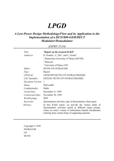
LPGD<br />
A Low-Power Design Methodology/Flow and its Application to the<br />
Implementation of a DCS1800-GSM/DECT<br />
Modulator/Demodulator<br />
(ESPRIT 25256)<br />
Title: “Report on the General IC&D”<br />
Author(s): D. Soudris 1 , C. Dre 2 , and C. Goutis 3<br />
1<br />
Democritus University of Thrace (DUTH)<br />
2<br />
Intracom<br />
3<br />
University of Patras (UP)<br />
Editor: DUTH+UP+INTRACOM<br />
Type: Report<br />
LPGD Id: LPGD/WP2/DUTH+UP+INTRACOM/D2R2<br />
CEC Identifier: EP25256/ DUTH+UP+INTRACOM/D2R2<br />
Document Version: 1<br />
Status: Deliverable<br />
Confidentiality: Public<br />
Actual Date: December 31, 1999<br />
Contractual Date: November 30, 1999<br />
WorkPackage: WP2<br />
Keywords: dissemination activities, type of dissemination, final report<br />
Abstract: In this IC&D report, we provide the various kinds of<br />
dissemination activities aimed at different target groups,<br />
where we used a variety of information transfer mechanisms<br />
realizing from certain forms of supporting material.<br />
Copyright © 1999<br />
INTRACOM<br />
UP<br />
DUTH
Report on the General IC&D LPGD/WP2/DUTH+UP+INTRACOM/D2R2<br />
History<br />
Date Version Comments<br />
December 31, 1999 1 Deliverable<br />
Purpose /Scope<br />
The purpose of the final Information Capturing and Dissemination report is to provide all the dissemination<br />
activities which done during the twenty four months of LPGD projects. The consortium through the different<br />
activities tried to disseminate the project results into a variety of target groups coming from academia and<br />
industry.<br />
Public Page 2
Report on the General IC&D LPGD/WP2/DUTH+UP+INTRACOM/D2R2<br />
TABLE OF CONTENTS<br />
1. INTRODUCTION ........................................................................................................................................ 4<br />
2. SUMMARY ................................................................................................................................................. 4<br />
2.1 GMSK DIGITAL MODULATOR...................................................................................................................... 4<br />
2.2 DECT RECEIVER......................................................................................................................................... 4<br />
2.3 FIR FILTER DESCRIPTION ............................................................................................................................ 6<br />
3. INFORMATION CAPTURING AND DISSEMINATION ACTIVITIES...................................................... 7<br />
3.1 EVENTS/PATMOS ’99 WORKSHOP.............................................................................................................. 7<br />
3.2 MEETINGS................................................................................................................................................... 7<br />
3.3 PUBLICATIONS............................................................................................................................................. 7<br />
3.4 AWARD....................................................................................................................................................... 9<br />
3.5 FUTURE PLANS ............................................................................................................................................ 9<br />
3.6 CONCLUSIONS ............................................................................................................................................. 9<br />
4. REFERENCES............................................................................................................................................. 9<br />
List Of Figures<br />
Figure 1. FPGA Interface ................................................................................................................................. 5<br />
Figure 2. The Architecture of DECT receiver. .................................................................................................. 6<br />
Table of Contents Public Page 3
Report on the General IC&D LPGD/WP2/DUTH+UP+INTRACOM/D2R2<br />
1. Introduction<br />
This report includes all the dissemination activities which done during the twenty four months of LPGD<br />
projects. The consortium through the different activities tried to disseminate the project results into a<br />
variety of target groups coming from academia and industry. The target group’s people were<br />
undergraduate and graduate students coming from universities and research institutes, professors from<br />
European and Northern America Universities, and designers and managers from industry. Depending on<br />
the audience, we used different information transfer mechanism. More specifically, we participated in the<br />
technical meetings and ESD-LPD workshop organized by DIMES, where we provided appropriate talks,<br />
we had close cooperation with DIMES during PATMOS 99 workshop where we organized common<br />
actions, we published a plethora of journals and conference papers and two book chapters, we established<br />
a functional web-sites to all partners, where all the public material (i.e. deliverable reports) can be<br />
downloaded, and we developed tools for power estimation. For supporting the dissemination activities we<br />
prepared many articles, demos for the developed software tools, and material for presentations.<br />
The rest of this report is organized as follows: Section 2 presented a summary the design experiment. The<br />
Section 3 presented all the IC&D activities done during the LPGD project. Some conclusions are drawn in<br />
Section 4.<br />
2. Summary<br />
Figure 1 depicts the main building blocks of the implemented GSM/DECT Modulator/Demodulator as<br />
well as the interface links or signals with ASPIS processor [1,2], the chosen Analog-to-Digital and<br />
Digital-to-Analog Converters, and Automatic Gain Control (AGC) & DC Offset. The main building<br />
blocks of the designed module are:<br />
i) the GSM/DECT modulator, based on a look-up-table principle which creates the GMSK<br />
waveforms,<br />
ii) the DECT demodulator, which is based in a zero-IF architecture, and<br />
iii) the digital FIR filters.<br />
The main characteristics of each building block of GMSK/GFSK modulator/demodulator will be given in<br />
the next paragraphs. The system description will begin with the uplink path and through downlink path,<br />
will end up with the detailed implementation of FIR filters.<br />
2.1 GMSK Digital Modulator<br />
The architecture of the digital GMSK modulator designed to satisfy both GSM and DECT standards. The<br />
modulator receives data from ASPIS processor and produces two output streams, I and Q, which are<br />
eventually the input of D/A converter.<br />
The input stream of GMSK Modulator, , comes from ASPIS processor, while the outcome of<br />
modulator is two GMSK modulated digital streams Iout and Qout of 10 bits. The input data of inData<br />
appear after (N+1/2)×Tb time units, where Tb is the period of Data_Clock and N integer ranging between<br />
0 and 511. The inData are read either with falling edges of Data_clock or before the use of phi clock<br />
8x1152kb/s. It can be stressed that the time point where the data of inData will be read is not so critical<br />
(i.e. enable of read In). The signal SynReset is activated during a falling-edge of Data_Clock. The rate of<br />
inData stream is equal to the rate GSM/DECT standard. Regarding with GSM and DECT, an<br />
interpolation factor 16 (=4.33MHz) and 8 (=9.2MHz) is used, respectively. Then, using a suitable<br />
multiplexer, the multiplexed data are feed to a Digital-to-Analog converter (DAC). The demonstrator<br />
board uses the DAC AD9761 of Analog Devices. This particular DAC has one parallel port of 10 bits,<br />
which read the multiplexed data of I & Q every rising edge of clock. The value of SELECT determines<br />
whether the current input value belongs to I or Q output streams. During the idle state the signals<br />
CLOCK/WRITE are LOW.<br />
2.2 DECT Receiver<br />
The complete design of the implemented DECT receiver, shown in Fig. 2, consists of four blocks:<br />
• The Phase Difference Decoder Block (PDD)<br />
Public Page 4
Report on the General IC&D LPGD/WP2/DUTH+UP+INTRACOM/D2R2<br />
• The Automatic Frequency Correction Block (AFC)<br />
• The Phase Difference Transition Mapper Block (PDTM)<br />
• The Symbol Timing Estimation Block (STE)<br />
ASPIS<br />
Processor<br />
t_en<br />
do<br />
H_mode<br />
b_clk<br />
EMI_clk<br />
bsclk<br />
r_en<br />
rec_data<br />
dpllsynchom<br />
slotsynchom<br />
aux_fso_out<br />
aux_do<br />
aux_fsin<br />
aux_fso_din<br />
aux_clk<br />
Aux Clock<br />
synReset<br />
inData<br />
gsmDect<br />
13.824MHz<br />
27.648MHz<br />
Start_Detection<br />
Symbol<br />
preamble_detected<br />
b_clk 13.824MHz<br />
Data_Clock<br />
slot_detected<br />
I/F<br />
Start_Detection<br />
LPGD FPGA 1<br />
I/F<br />
phi<br />
8x1152kHz<br />
GMSK<br />
Digital<br />
Modulator<br />
Clock<br />
generator<br />
block<br />
DECT<br />
Detector Receiver<br />
6<br />
Select<br />
6<br />
6 6 8 8<br />
8<br />
8<br />
AGC &<br />
DC offset block<br />
FIR<br />
FIR<br />
10<br />
10<br />
2<br />
Clock<br />
4x1152kHz<br />
Clock<br />
4x1152kHz<br />
Figure 1. FPGA Interface<br />
8<br />
8<br />
MUX<br />
DEMUX<br />
FPGA 2<br />
I/F<br />
readIn<br />
IQ 10bits<br />
SELECT<br />
WRITE<br />
CLOCK<br />
CLOCK<br />
SELECT<br />
IQ 8bits<br />
CS<br />
SCLK<br />
DIN<br />
AD9761<br />
AD9281<br />
Input<br />
Streams<br />
MAX549A<br />
Output<br />
Streams<br />
The circuit accepts at its input a quantized IQ stream consisting of a pair (I, Q) of 6-bit vectors in sizemagnitude<br />
form received on each clock cycle. The processing of the above stream by the five blocks<br />
presented above yields the bit stream of the data section contained in a DECT slot. More specifically, the<br />
differential detector uses the symbol rate sampled streams of the in-phase, I, and quadrature-phase, Q,<br />
components of the received baseband GMSK signal and calculates the phase difference between the two<br />
sampling instants. The AFC system operates using one sample per symbol period and estimates the phase<br />
rotation between two successive symbols, and produces a phase error estimate that corrects the phase<br />
difference.The phase difference, after being corrected by the AFC block, is fed to the Phase Difference<br />
Transition Mapper (PDTM). This block, depending on the phase difference, will produce a 01, 10 or 00,<br />
which in turn, with the help of a simple FSM, will extract the estimated data. Finally, the functions of slot<br />
synchronization and symbol timing estimation block of the proposed receiver use the same basic<br />
principles. As a result, these functions are implemented by the same functional block and occur<br />
simultaneously, thus resulting in a joint slot Synchronization and symbol timing estimation. The detailed<br />
functional description of DECT detector were presented in [3].<br />
In order to design efficiently the DECT receiver in terms of power consumption, we used existing<br />
low power techniques and developed two new power optimization techniques, namely the behavioural<br />
power management and the dynamic frequency reduction. These techniques can be applied on a large<br />
class of wireless communications algorithms. The power management discipline implies that when the<br />
output of a component becomes unobservable then this component can be shutdown [4]. The technique<br />
applied here is based on the fact that unobservability can be introduced for a behavioural cluster after the<br />
occurrence of an event. For example the outputs of a behavioural cluster responsible for the computation<br />
of a series become unobservable once the series converges. The same situations can be met in a<br />
behavioural cluster responsible for synchronization after the synchronization is achieved. The application<br />
of this technique achieves 31% power reduction for the DECT receiver circuit with respect to the power<br />
consumption of the DECT receiver circuit with no power management features.<br />
OUT I<br />
OUT Q<br />
Public Page 5
Report on the General IC&D LPGD/WP2/DUTH+UP+INTRACOM/D2R2<br />
The second technique reduces the frequency operation depending on the input data streams. More<br />
specifically, adaptive sampling through oversampling imposes that the whole receiving algorithm is<br />
computed on N input data streams, each one of which corresponds to a different sampling instance during<br />
the symbol period, while only one stream corresponds to the correct sampling instance. This introduces a<br />
significant power overhead. For this purpose a novel frequency reduction technique is introduced.<br />
Specifically, the operation frequency can be reduced to the symbol frequency after the synchronization<br />
pattern detection and up to the end of the frame. During this time interval, the receiver is forced to<br />
operate only on the input stream that corresponds to the correct sampling instance. After the end of each<br />
frame the receiver operates again at the oversampling frequency. For the design of the DECT receiver<br />
design, the application of dynamic frequency reduction lead to 65% power reduction, with an area<br />
overhead of 1,02%.<br />
Table 1 gives the area estimation, the number of equivalent gates and the power dissipation of each<br />
block separately as well as the total power consumption of DECT receiver.<br />
6 Bits<br />
6 Bits<br />
CLOCK<br />
CONTROL<br />
PHASE<br />
DIFFERENCE<br />
DETECTOR<br />
2.3 FIR Filter Description<br />
2<br />
SYMBOL TIMING<br />
ESTIMATION<br />
8<br />
AUTOMATIC<br />
FREQUENCY<br />
CORRECTION<br />
8<br />
DECT<br />
RECEIVER<br />
PHASE<br />
TRANSITION<br />
MAPPER<br />
Figure 2. The Architecture of DECT receiver.<br />
Filtering in most digital communication systems is accomplished by a combination of analog and digital<br />
lowpass filters. Digital lowpass filters are designed as Finite Impulse Response (FIR) filters. In this way<br />
there is more flexibility in the design and on the other hand it is a lot easier to obtain some very desirable<br />
characteristics like phase linearity and high accuracy in the response. Usually some windowing methods<br />
are used to derive the coefficients of the impulse response of the FIR filter. It should be stressed here that<br />
during the design of FIR filters the features of the analog filters of the uplink and downlink path were<br />
taken into account. Particularly, the receiver part uses 4th order Butterworth antialiasing analog filter,<br />
with fc=0.8*R. After extensive simulations we have reached the conclusion that a 13 taps FIR filters with<br />
interpolation factor 4 and cut-off frequency approximately 0.6*R(691xMHz) yields satisfactory<br />
performan-ce (BER results vs. SNR or Eb/N0). In addition, they meet the specifications of the DECT<br />
standard. Finally, it should be mentioned that a Kaiser window with beta=3.5 has been used.<br />
The input and the output of FIR are 8-bit sign magnitude integer (MSB is the sign and the seven LSBs<br />
is the value of signal). To attain sufficient accuracy and avoid the overflow possibility the internal buses<br />
have 24-bit length.<br />
Since the given coefficients are real numbers between –1 and 1, possible filter implementation with<br />
these coefficients would require a floating-point architecture. For that purpose, to simplify the design, a<br />
scaling technique is used to convert the filter coefficients into integer numbers. Thus, all the coefficients<br />
are multiplied by 16384. Because of these multiplications, the output of FIR multiplied with 16384, the<br />
output should be divided by 16384.<br />
We implemented the FIR filter using Cadence environment. After synthesis and simulation, we<br />
concluded that the FIR operates with 4.608 MHz clock frequency, the area is 7.075mm 2 using 0.7 m<br />
technology.<br />
Public Page 6
Report on the General IC&D LPGD/WP2/DUTH+UP+INTRACOM/D2R2<br />
3. Information Capturing and Dissemination Activities<br />
3.1 Events/PATMOS ’99 Workshop<br />
In the context of 9th International Workshop on Power And Timing, Modeling, Optimization, Simulation<br />
(PATMOS ’99), 6-8 October, 1999 and the Digital Interest Group Meeting at Kos, October 5, 1999,<br />
PATMOS organizing committee (Note: The Contact person for IC&D of LPGD was also the General<br />
Chair of PATMOS 99) and DIMES had very effective cooperation and organized two very attractive panel<br />
sessions.<br />
More specifically, a panel session entitled “Does Logic Design only requires software skills?” took place<br />
an the 5th October 1999 in Kos, Greece. The Coordinator was Prof. Christian Piguet, CSEM, Switzerland<br />
and the panelists were: i) Professor W. Nebel, Uni-Oldenburg, Germany for “CAD for low-power”, ii)<br />
Professor D. Auvergne, LIRMM, France for “Teaching”, and iii) Ed Huigbrechts, Philips, Netherlands,<br />
for “Low-Power IC design”.<br />
The second panel was coordinated by Prof. Reinder Nouta and Rene van Leuken, DIMES in 7th October<br />
1999 ESD-LPD in Kos, Greece. Its title was "Power Analysis/Estimation Tools: Experiences and<br />
Expectations” and panelists were excellent experts from industry and academia; i) Prof. Steve Furber,<br />
Univ. of Manchester, UK, ii) Dr. Ed Huijbregts, PHILIPS, iii) Beata Paige, SENTE, and iv) Prof. Enrico<br />
Macii, Politecnico di Torino, ITALY.<br />
3.2 Meetings<br />
LPGD people participated actively in a series of technical meetings/workshops of the Digital Interest<br />
Group, which were organized by DIMES, TU Delft. Below, we provided the completed list of the<br />
technical meetings with the corresponding participants.<br />
i) Digital Interest Group Workshop at Sheraton Amsterdam Airport Hotel, July2, 1998.<br />
Participants: Dr. Dimitris Dervenis, Intracom.<br />
ii) Digital Interest Group Workshop at Sheraton Amsterdam Airport Hotel, November 23-24, 1998.<br />
Participants: Professor C.E. Goutis, University of Patras and Ass. Prof. D. Soudris, Democritus Univ.<br />
of Thrace.<br />
iii) Digital Interest Group Workshop and the ESD-LPD Open Workshop at Como, March 3, 1999.<br />
Participants: Professor C.E. Goutis, University of Patras and Ass. Prof. D. Soudris, Democritus Univ.<br />
of Thrace.<br />
iv) Digital Interest Group Workshop and the ESD-LPD Open Workshop at Kos, October 5, 1999. During<br />
the Open Part of Workshop a presentation of 30 min about the research results of LPGD was given by<br />
Ass. Prof. D. Soudris, , Democritus Univ. of Thrace and N. Zervas, University of Patras.<br />
Participants: Professor C.E. Goutis and N. Zervas, University of Patras, Ass. Prof. D. Soudris and<br />
Prof. A. Thanailakis, Democritus Univ. of Thrace, and Dr. C. Dre, INTRACOM.<br />
3.3 Publications<br />
During LPGD project several kinds of documents, which covered various aspects of the design<br />
experiment, the new low power design and estimation techniques, the design methodology for wireless<br />
applications and the main characteristics of the developed software tools, were published. Three kinds of<br />
publications were used: i) Public RDP and ICD Deliverables, ii) Journal papers, and iii) Conference<br />
papers. All the public material is available at the following sites of:<br />
INTRACOM: http://www.intracom.gr/lpgd<br />
UP: http://www.vlsi.ee.upatras.gr/Projects/lpgd/lpgd_pubs.html<br />
DUTH: http://www.vlsi.ee.duth.gr/projects/lpgd/lpgd_pubs.html<br />
Public Deliverables<br />
Public RDP Deliverables:<br />
i) D1.1R1: Survey of Low-Power Techniques,<br />
ii) D1.2R1: Structure of the Low-Power Design Flow,<br />
iii) D1.3R1: Generalised Low-Power Design Flow,<br />
iv) D2.1R1: Study, Analysis, and Exploration of Candidate Algorithms,<br />
v) D2.2R1: Low-Power Methodology for Transformations of Wireless Communication Algorithms,<br />
vi) D3.2R1: Low-Power Methodology for Designing Multiple Filters, and<br />
vii) D4.1R2: Report on Demonstration in DECT & GSM/DCS Environment.<br />
Public Page 7
Report on the General IC&D LPGD/WP2/DUTH+UP+INTRACOM/D2R2<br />
Public IC&D Deliverables:<br />
i) D1R1 Proceedings of first Workshop,<br />
ii) D1R2 Proceedings of second Workshop,<br />
iii) D1R3 Dissemination results,<br />
iv) D2R1: Structure and techniques of the Low Power Design Flow, and<br />
v) D2R2: Report on the General IC&D.<br />
Journal/Conference Papers<br />
Regarding with the research results of LPGD a number of journal and conference papers were published,<br />
as the following list:<br />
Journal Papers<br />
1. G. Theodoridis, S. Theoharis, D. Soudris, and C.E. Goutis, “A Probabilistic Power Estimation Method<br />
for Combinational Circuits Under Real Gate Delay Model,” accepted for presentation in VLSI Design,<br />
Journal of Custom-Chip Design, Simulation, and Testing (invited paper).<br />
2. S. Theoharis, G. Theodoridis, P. Merakos, and C. Goutis, “Accurate Data Path Models for Fast RTlevel<br />
Power Estimation,” accepted for publication in IEE Proceedings - Circuits, Devices and Systems.<br />
Conference Papers<br />
1. D. Soudris, M. Perakis, X. Mizas, V. Mardiris, K. Katis, C. Dre, A.E. Tzimas, E.G. Metaxakis, G.<br />
Kalivas, N. Zervas, S. Theoharis, G. Theodoridis, A. Thanailakis, and C. Goutis, “Low-Power Design<br />
Of A Multi-Mode Transceiver,” accepted for presentation at ISCAS 2000, May 28 - 31, Geneva,<br />
Switzerland.<br />
2. N. Zervas, D. Soudris, S. Theoharis, C.E. Goutis, and A. Thanailakis, “A Methodology for the<br />
Behavioral-Level Event-Driven Power Management of Digital Receivers,” accepted for presentation at<br />
ISCAS 2000, May 28 - 31, Geneva, Switzerland.<br />
3. D.Soudris, N.D. Zervas, M. Perakis, S. Theoharis, G. Theodoridis, G. Kalivas, C. Dre, C.E. Goutis,<br />
and A. Thanailakis, “On the Low Power Design of Digital Receivers for Wireless Applications,”<br />
accepted for presentation in DATE 2000 User Forum, Paris, 27 - 30 March 2000.<br />
4. D. Soudris, C. Z. Lolas, and A. Thanailakis, “A Modified Energy Recovery Technique For<br />
Implementing DSP Algorithms,” accepted for presentation in 9th Int. Workshop Power And Timing<br />
Modeling, Optimization And Simulation (PATMOS `99), Kos, Greece, October 6-8, 1999, pp. 113-<br />
122.<br />
5. Z. Lolas, D. Soudris, I. Karafyllidis, A. Thanailakis, “A New Adiabatic Technique for Designing Low<br />
Power Array Architectures,” in Proc. of Int. Conf. on Electronics, Circuits and Systems (ICECS ’99),<br />
September 5-8, 1999, Pafos, Cyprus, pp. 795-798.<br />
6. M. Perakis, A.E. Tzimas, E.G. Metaxakis, D. Soudris, G.A. Kalivas, C. Katis, C. Dre, C.E. Goutis,<br />
and A. Thanailakis, “The VLSI Implementation Of A Baseband Receiver For Dect-Based Portable<br />
Applications,” in Int. Symp. on Circuits and Systems (ISCAS), Orlando, Florida, USA, May 30 - June<br />
2, 1999, Vol. I pp. 198-201.<br />
7. S.Theoharis, G. Theodoridis, D. Soudris, and C.E. Goutis,“An Efficient Probabilistic Method for<br />
Logic Circuits Using Under Real Delay Gate Model”, in Int. Symp. on Circuits and Systems (ISCAS),<br />
Orlando, Florida, USA, May 30 - June 2, 1999, Vol. I pp. 258-261.<br />
8. C.Z. Lolas, D. Soudris, I. Karafyllidis, And A. Thanailakis, “A New Adiabatic Technique For<br />
Designing Low Power Array Architectures”, In Proc. Of 6th IEEE Int. Conf. On Electronics, Circuits,<br />
And Systems (ICECS), September 5-8, Pp. 795-798, Pafos, Cyprus, 1999.<br />
9. S. Theoharis, G. Theodoridis, D. Soudris, and C.E. Goutis, "Accurate Data Path Module for RT Level<br />
Power Estimation" in Proc. of 8th Int. Workshop Power and Timing Modeling, Optimization and<br />
Simulation (PATMOS `98), pp. 213-222, October 7-9, Lyngby, Denmark.<br />
10. A.E. Tzimas, E.G. Metaxakis, and G.A. Kalivas "The design of a Baseband Receiver for a zero-IF<br />
DECT System Architecture" presented in Communication Systems of DSP, Sheffield, UK, 1998.<br />
11. A.E. Tzimas, E.G. Metaxakis, and G.A. Kalivas "A Low complexity Baseband Receiver for direct<br />
conversion Burst-type radio System" presented in Int. Sympos. on Computers and Communications<br />
(ISCC) Athens, Greece, 1998.<br />
12. E.G. Metaxakis, A.E. Tzimas, G.A. Kalivas, and G. Papadopoulos, "A Low complexity Baseband<br />
Receiver for direct conversion DECT-based Portable Communications" accepted for presentation in<br />
Int. Conf. on Universal Personal Communications (ICUMP), Florence, Italy, 1998.<br />
Public Page 8
Report on the General IC&D LPGD/WP2/DUTH+UP+INTRACOM/D2R2<br />
Software Demostration<br />
During DATE 2000, we provide a demonstration of a software power estimation tool.<br />
3.4 Award<br />
The entire technical description of LPGD results (about 4,000 words) was submitted for review in Low<br />
Power Design Contest of 2000 IEEE Computer Elements Mesa Workshop, January 16-19 2000, Arizona.<br />
Our contribution selected and received an award of 2,000$ sponsored by Intel and IBM.<br />
3.5 Future Plans<br />
Our participation in Low Power Design Cluster and especially in LPGD project provides us with<br />
significant experiences, due to a variety of activities. Although LPGD project was completed by the end<br />
of October 1999, as consortium are willing to provide (and we provide) all the additional manpower for<br />
further dissemination of the gain experiences and the scientific results.<br />
i. According to the discussions in last ESD-LPD meetings, we have started preparing two book chapters,<br />
which are LPGD contributions in the book with the tentative title “Unified low-power design flow for<br />
data-dominated multimedia and telecom applications”, whose editor is Prof. F. Catthoor, IMEC,<br />
Belgium. The titles of our contributed chapters are:<br />
a) “Unified low-power design flow for data-dominated multimedia and telecom applications”<br />
b) "Power efficient synthesis of sum-of-products computations", with authors K. Masselos and C. E.<br />
Goutis.<br />
ii. The schedule is to prepare the whole book within the summer of 2000.<br />
iii. In addition, a second book will be prepared, with editor the Prof. Peter Ivey, Univ. of Sheffield, United<br />
Kingdom. LPGD will contribute a chapter about logic-level low power design techniques and power<br />
estimation methods. We hope finishing that work by end of this year.<br />
iv. During ESD-LPD'00 Workshop, Portofino, Italy, July 25-28, 2000, one presentation will be organized.<br />
v. Two journal papers are preparing for submission to: IEEE Trans. on Circuits and Systems II and IEEE<br />
Trans. on VLSI.<br />
3.6 Conclusions<br />
In the approved Technical Annex of IC&D, we have promised a series of activities, which would satisfy<br />
not only the general goals of IC&D action but also the IC&D activities described in the Technical Annex<br />
of IC&D. The various kinds of dissemination activities aimed at different target groups, where we used a<br />
variety of information transfer mechanisms realizing from certain forms of supporting material.<br />
A large variety of dissemination activities were made during the accomplishment of LPGD project.<br />
Comparing these activities with ones described in Technical Annex of IC&D, it can be easily inferred that<br />
the consortium made more activities that the promised ones without any additional expenses. Since LPGD<br />
partners have strong links through many other activities, the dissemination will continue as it can be seen<br />
in subsection 3.5, which indicates that the partners will provide all the necessary manpower to continue<br />
the dissemination the developed low power techniques and methodologies beyond the end of LPGD<br />
project.<br />
In conclusion, the partners of LPGD (INTRACOM SA, University of Patras, and Democritus University<br />
of Thrace) through the plethora of IC&D activities mentioned in Section 2-6 fulfilled entirely the<br />
objectives of IC&D Technical Annex and participated actively in more activities than the ones promised<br />
in IC&D Technical Annex of LPGD.<br />
4. References<br />
[1] D. Moolenaar, 'Building Blocks Preliminary Design Report (Processor Core)', ASPIS project deliverable,<br />
EP20287/IMEC/VSDM/DS/D4.2.R1/a1, May 1997.<br />
[2] H.C. Karathanasis, V. Bella, S. Blionas, D. Dervenis, C. Dre, 'Market Input Report for Multi-mode Terminal<br />
Specifications', ASPIS project deliverable, P20287/ ICOM/DPD/DS/D6.1.R1/a1, Version 4, 15 June 1996.<br />
[3] M. Perakis, A.E. Tzimas, E.G. Metaxakis, D. Soudris, G.A. Kalivas, C. Katis, C. Dre, C.E. Goutis,<br />
and A. Thanailakis, “The VLSI Implementation of a Baseband Receiver For DECT-Based Portable<br />
Applications,” in Int. Symp. on Circuits and Systems (ISCAS), Orlando, Florida, USA, May 30 -<br />
June 2, 1999, Vol. I pp. 198-201.<br />
Public Page 9
Report on the General IC&D LPGD/WP2/DUTH+UP+INTRACOM/D2R2<br />
[4] N.Zervas, D. Soudris, S. Theoharis, C.E. Goutis, and A. Thanailakis, A Methodology for the<br />
Behavioral-Level Event-Driven Power Management of Digital Receivers, accepted for<br />
presentation at ISCAS 2000, May 28 - 31, Geneva, Switzerland.<br />
Public Page 10