Orion - Single Channel - OpenWrt Wiki
Orion - Single Channel - OpenWrt Wiki
Orion - Single Channel - OpenWrt Wiki

Create successful ePaper yourself
Turn your PDF publications into a flip-book with our unique Google optimized e-Paper software.
<strong>Orion</strong> - <strong>Single</strong> <strong>Channel</strong><br />
SDSL, HDSL2, or SHDSL - ILD2<br />
Overview<br />
The Conexant <strong>Orion</strong> Digital Subscriber Line (DSL) chip sets provide<br />
low power, high density solutions for 2-wire DSL equipment. These<br />
chip sets are fully programmable and field upgradeable eliminating the<br />
risk of product obsolescence and accelerating the time-to-market for<br />
new network services. The Conexant <strong>Orion</strong> DSL chip sets are fully<br />
interoperable with multi-vendor DSL chip set solutions. This<br />
interoperability enables dynamic interworking of multiple vendor DSL<br />
solutions with the capability to interoperate with products that conform<br />
to ANSI and ETSI DSL standards.<br />
Conexant’s unique hardware platform supports multiple singlechannel<br />
applications including SDSL, HDSL2, and SHDSL, using<br />
population options for optimization.<br />
The <strong>Orion</strong> DSL chip sets incorporate two DSL bit pumps plus framing<br />
into a three-chip solution comprised of a single-channel digital signal<br />
processor (DSP) with built-in framer and an Analog Front End (AFE)<br />
with an Integrated Line Driver (ILD2).<br />
The <strong>Orion</strong> chip sets interface directly with off-the-shelf T1/E1<br />
transceivers eliminating the need for a separate DSL framer to<br />
combine and format the DSL channel into a standard interface.<br />
Conexant’s DSL <strong>Orion</strong> chip sets deliver one channel of full duplex<br />
transmission up to 5704 kbps, depending on the application.<br />
The high density <strong>Orion</strong> single-channel DSL chip sets are ideal for CPE<br />
applications, while dual-channel versions with integrated framer are<br />
also available for CO applications.<br />
Customer Interface<br />
TDATA<br />
TClock<br />
Frame Pulse<br />
RDATA<br />
Rclock<br />
Frame Pulse<br />
μProcessor Interface<br />
<strong>Single</strong><br />
<strong>Channel</strong><br />
DSP<br />
w/Framer<br />
ILD2<br />
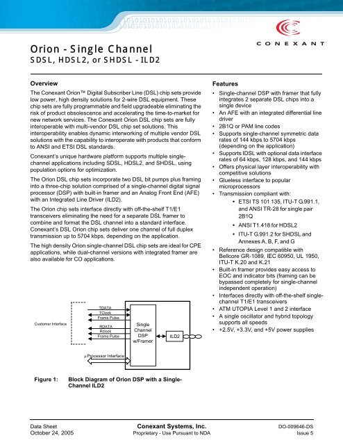
Figure 1: Block Diagram of <strong>Orion</strong> DSP with a <strong>Single</strong>-<br />
<strong>Channel</strong> ILD2<br />
Features<br />
• <strong>Single</strong>-channel DSP with framer that fully<br />
integrates 2 separate DSL chips into a<br />
single device<br />
• An AFE with an integrated differential line<br />
driver<br />
• 2B1Q or PAM line codes<br />
• Supports single-channel symmetric data<br />
rates of 144 kbps to 5704 kbps<br />
(depending on the application)<br />
• Supports IDSL with optional data interface<br />
rates of 64 kbps, 128 kbps, and 144 kbps<br />
• Offers physical layer interoperability with<br />
competitive solutions<br />
• Glueless interface to popular<br />
microprocessors<br />
• Transmission compliant with:<br />
• ETSI TS 101 135, ITU-T G.991.1,<br />
and ANSI TR-28 for single pair<br />
2B1Q<br />
• ANSI T1.418 for HDSL2<br />
• ITU-T G.991.2 for SHDSL and<br />
Annexes A, B, F, and G<br />
• Reference design compatible with<br />
Bellcore GR-1089, IEC 60950, UL 1950,<br />
ITU-T K.20 and K.21<br />
• Built-in framer provides easy access to<br />
EOC and indicator bits (framing can be<br />
bypassed completely for single-channel<br />
independent operation)<br />
• Interfaces directly with off-the-shelf singlechannel<br />
T1/E1 transceivers<br />
• ATM UTOPIA Level 1 and 2 interface<br />
• A single oscillator and hybrid topology<br />
supports all speeds<br />
• +2.5V, +3.3V, and +5V power supplies<br />
Data Sheet Conexant Systems, Inc. DO-009646-DS<br />
October 24, 2005 Proprietary - Use Pursuant to NDA Issue 5
<strong>Orion</strong> <strong>Single</strong> <strong>Channel</strong> Data Sheet October 24, 2005<br />
Introduction<br />
The Conexant DSL chip sets support applications ranging<br />
from remote network access, digital pair gain, video<br />
conferencing, and cellular base station land-line<br />
connectivity, for T1/E1 services. Up to 36 voice circuits<br />
may be provisioned over a single copper pair.<br />
Example Applications<br />
• Compatibility with voice/data pair gain systems<br />
• Cellular and microcellular systems<br />
• T1/E1 and fractional T1/E1 DSL transceiver<br />
• Wireless base station connectivity<br />
Related Materials<br />
To accelerate time-to-market, Conexant offers our<br />
customers a comprehensive Design Guide which includes<br />
details on planning, layout, testing, debugging, and expert<br />
tips and recommendations for building a successful DSL<br />
product. The Design Guide is distributed as part of a<br />
Design Package which includes firmware, transceiver<br />
schematics, sample code, transceiver layout Gerber files,<br />
and Bill of Materials.<br />
For rapid prototyping, Quick Kits are available. These<br />
Quick Kits contain all transceiver design BOM<br />
components in kit form so there’s no component lead time<br />
delay.<br />
The SGDSTM development system, an easy-to-use<br />
evaluation and development platform designed to support<br />
all Conexant xDSL transceiver solutions, is also available<br />
for early product development.<br />
The SGDS also provides an interface to the Conexant<br />
Microsoft ® Windows ® — based Host Interface Program<br />
(WHIP). When the SGDS is teamed with WHIP, product<br />
evaluation, testing and debugging is achieved with the<br />
click of a mouse.<br />
Conexant Transceiver System Overview<br />
• The Conexant <strong>Orion</strong> DSL chip sets consist of a singlechannel<br />
DSP with an on-chip framer, and a singlechannel<br />
AFE (with ILD2).<br />
• The single-channel ILD2 filters and digitizes the signal<br />
received on the telephone line and for the transmit<br />
side, generates analog signals from the digital data<br />
and filters the analog signals to create the 2B1Q or<br />
PAM transmit signal (depending on the line code).<br />
• The Conexant Windows-based Host Interface<br />
Program (WHIP) is offered as part of the Conexant<br />
transceiver system development package for SDSL<br />
2B1Q, HDSL2, and SHDSL applications. WHIP<br />
allows you to test and debug your product design with<br />
the click of a mouse. This graphical interface allows<br />
you to send commands, perform trace and debug<br />
procedures, and initiate a startup on both the CO and<br />
CP units. WHIP offers complete flexibility and<br />
modularity. You can rearrange windows and toolbars<br />
to suit your preferences and design requirements.<br />
Conexant Systems, Inc. DO-009646-DS<br />
2 Proprietary - Use Pursuant to NDA Issue 5
October 24, 2005 <strong>Orion</strong> <strong>Single</strong> <strong>Channel</strong> Data Sheet<br />
Architecture<br />
The interface between the Host and the transceiver<br />
consists of the following:<br />
• Transmission Interface (data, clock and<br />
synchronization signals)<br />
• Control Interface (microprocessor compatible)<br />
• Diagnostic Interface<br />
• Power Interface<br />
• Loop Interface<br />
System timing is derived from a free running oscillator in<br />
the transceiver of the central office (CO). At the customer<br />
premises end (CPE), the CPE derives a clock from the<br />
received line signal and provides this clock to the CPE<br />
transmitter.<br />
The single-channel chip set also supports Network Timing<br />
Recovery (NTR) at the CO end. With this feature enabled,<br />
the CO unit will accept a clock at 8 kHz (± 100 ppm) as an<br />
input and the STU-R will output a clock that is phase<br />
locked to the CO clock. The NTR clock should have a duty<br />
cycle of 45-55%. Note that this feature is only available<br />
with an UTOPIA interface.<br />
The DSL transceiver supports both T1 and E1 rates, and<br />
fractional rates.<br />
Transceiver States<br />
The following is a list of the possible states that the DSL<br />
transceiver can be in:<br />
• IDLE mode, where the transceiver is not attempting to<br />
start up, pass data, or perform tests<br />
• TEST mode, where the transceiver is either in local<br />
analog loopback or local digital loopback and is not<br />
passing user data<br />
• STARTUP mode (SDSL only), where the transceiver<br />
is attempting a startup of the DSL connection, prior to<br />
entering DATA mode<br />
• HANDSHAKE mode (HDSL2 and SHDSL), where a<br />
link is established between the CO unit and the CPE<br />
unit<br />
• TRAINING mode (HDSL2 and SHDSL), where the<br />
transceiver is attempting a startup, prior to entering<br />
DATA mode<br />
• DATA mode, where the transceiver has started up<br />
and trained and is capable of passing user data<br />
Software Interface<br />
A microprocessor interface that uses simple read/write<br />
drivers provides direct access to the Conexant chip set -<br />
eliminating the need for complicated register maps and<br />
advanced programming. These drivers allow the Host to<br />
select rates, adjust transmit power, read signal quality,<br />
and perform a variety of other tasks which include<br />
reporting the current operational status of the transceiver.<br />
To configure and control the transceiver, Conexant<br />
provides hardware-dependent driver examples and<br />
Conexant supplied transceiver software modules (TSMs).<br />
The TSMs have the ability to allow a single CPU in the<br />
Host to control multiple transceivers. This could be a<br />
potential cost savings for arrangements where it might be<br />
advantageous to put multiple transceivers on one card,<br />
such as at the CO.<br />
NOTE:<br />
You will not need a register map of the DSP, as this<br />
information is not required to successfully design and<br />
implement an STU. As discussed previously, access<br />
to the DSP is provided through hardware-dependent<br />
I/O routines and Conexant provided TSMs.<br />
DO-009646-DS Conexant Systems, Inc.<br />
Issue 5 Proprietary - Use Pursuant to NDA 3
<strong>Orion</strong> <strong>Single</strong> <strong>Channel</strong> Data Sheet October 24, 2005<br />
Retrain<br />
IDLE<br />
MODE<br />
Data Mode<br />
Abort<br />
Host Processes<br />
BOOT<br />
LOAD<br />
(not timed)<br />
Set all<br />
framer<br />
options<br />
DSP/Framer Interrupt Received<br />
Optional<br />
SStatusXCVR()<br />
GTI_ACTIVE<br />
HANDSHAKE<br />
Power Up<br />
InitXCVR_CS()<br />
Reset DSP<br />
InitXCVR()<br />
SetParamXCVR()<br />
Optional<br />
SetParamFramer()<br />
ExecuteXCVR()<br />
Data Mode<br />
DETAIL A:<br />
FAILED STARTUP<br />
May occur anytime<br />
before Data Mode.<br />
DSP INTERRUPTS<br />
Idle Mode<br />
Idle Mode<br />
Idle Mode<br />
STARTUP MODE<br />
TRAINING<br />
Power Up<br />
Activities<br />
Power Up/<br />
Reset DSP<br />
Start Up<br />
Activities<br />
GTI_COMPLETE_PASS<br />
FRAME<br />
R<br />
SYNC*<br />
DETAIL A<br />
DATA MODE<br />
FRAMER INTERRUPTS<br />
* Only if PLL is enabled<br />
Figure 2: Typical Transceiver Power Up/Start<br />
Up Sequence<br />
Transceiver Start Up Sequence<br />
Figure 2 describes a typical sequence from power up to<br />
DATA mode for a transceiver. After power is applied to<br />
both the Host and the transceiver, the Host calls the<br />
InitXCVR_CS() and InitXCVR() routines to initialize<br />
transceiver variables and to initialize the DSP/Framer.<br />
Next, the Host calls the SetParamXCVR() routine to set<br />
up the parameters that are appropriate for start up of the<br />
transceiver.<br />
The SetParamFramer() routine is called by the Host to<br />
initialize framer options.<br />
After setting up the transceiver parameters, the Host calls<br />
the ExecuteXCVR() routine to execute the command<br />
that was set up using the SetParamXCVR() routine. With<br />
a successful completion of the ExecuteXCVR() routine,<br />
the transceiver will now be in DATA mode.<br />
The SStatusXCVR() routine is used to track<br />
performance and to obtain information from the<br />
transceiver about what state the transceiver is in (i.e.,<br />
monitor start-up, check signal quality, etc.).<br />
Setting Up the Command Parameters<br />
[SetParamXCVR()]<br />
The routine SetParamXCVR() processes the parameter<br />
array structure that will be executed when the<br />
ExecuteXCVR() routine is called.<br />
The parameter structure will be similar to the following<br />
start-up example:<br />
struct PARAM_XCVR_ARRAY Items;<br />
Items.length = GTI_NUM_OF_CMD_PARAMETERS<br />
Items.item[GTI_ACTION_ITEM]=GTI_STARTUP_REQ;<br />
Items.item[GTI_MODE_ITEM]=GTI_CO;<br />
Items.item[GTI_POWER_SCALE_ITEM]=GTI_DEFAULT_SCALE;<br />
Items.item[GTI_FRAMER_TYPE_ITEM]= GTI_UTOPIA_L2;<br />
.<br />
.<br />
.<br />
Conexant Systems, Inc. DO-009646-DS<br />
4 Proprietary - Use Pursuant to NDA Issue 5
October 24, 2005 <strong>Orion</strong> <strong>Single</strong> <strong>Channel</strong> Data Sheet<br />
Table 1 describes the example arguments to the<br />
SetParamXCVR() routine when performing start-up.<br />
This is only a sample subset of possible parameters,<br />
provided to illustrate how easy it is to work with the<br />
Conexant chip sets.<br />
Table 1: Example SetParamXCVR() Structure<br />
Parameter Function<br />
GTI_ACTION_ITEM The action GTI_STARTUP_REQ begins<br />
start-up, which, upon successful<br />
completion, results in the transceiver<br />
changing into DATA mode.<br />
GTI_MODE_ITEM Mode describes which transceiver the<br />
Host is talking to, the CO or CP.<br />
GTI_POWER_SCALE_ITEM Allows the transmit power to be set in<br />
small increments.<br />
GTI_FRAMER_TYPE_ITEM The framing modes are interface specific.<br />
Possible arguments for framing modes,<br />
depending on the customer interface,<br />
include: No Framing, UTOPIA Level 1,<br />
UTOPIA Level 2, T1, E1, and nxDS0<br />
(with the ability to choose continuous<br />
DS0 blocks).<br />
Checking the Transceiver Status<br />
[SStatusXCVR()]<br />
The SStatusXCVR() routine can be executed when in<br />
DATA mode, utilizing minimal processing power. To<br />
further illustrate the ease of programming Conexant chip<br />
sets, Table 2 supplies a few examples of<br />
SStatusXCVR().<br />
Table 2: Example SStatusXCVR() Parameters<br />
Parameter Function<br />
GTI_XMIT_POWER This action returns the transmitted power.<br />
GTI_START_PROGRESS The current detailed start-up state of the<br />
transceiver is returned.<br />
GTI_BERT_ERROR The number of bit errors detected during<br />
the 511 BERT test is returned.<br />
GTI_RECEIVER_GAIN Total receiver gain setting can be<br />
calculated using the return values from<br />
this action.<br />
DO-009646-DS Conexant Systems, Inc.<br />
Issue 5 Proprietary - Use Pursuant to NDA 5
<strong>Orion</strong> <strong>Single</strong> <strong>Channel</strong> Data Sheet October 24, 2005<br />
System Power Requirements<br />
The 160 PBGA <strong>Single</strong>-channel DSP/Framer chip requires +2.5V (±5%) and +3.3V (±5%), and the ILD2 chip require<br />
+3.3V (±5%) as well as +5V (±5%). Power requirements, including transceiver power consumption, have a tolerance<br />
of ±5%.<br />
The transceiver obtains its power from the power feed in the Host through the power interface. Table 3, Table 4, and<br />
Table 5 provide power requirements for the 160 PBGA <strong>Single</strong>-channel DSP.<br />
Table 3: Typical SDSL 2B1Q System Power<br />
Consumption Per <strong>Channel</strong> (DSP/Framer<br />
in a 160 PBGA)<br />
Line Rate<br />
(kbps)<br />
2.5VD<br />
DSP Core<br />
Drain Current (mA)<br />
3.3VD<br />
DSP &<br />
ILD2<br />
5VA<br />
ILD2<br />
NOTE:<br />
1. Power per channel based on dual-channel<br />
operation<br />
2. Based on customer schematic:<br />
G-02-2302-1006C-02 using 1:2 transformer<br />
Add 30 mA at 5VA for unified designs based on<br />
SHDSL population option G-02-2302-1006C-03<br />
using 1:4 transformer or HDSL2 population option<br />
G-02-2302-1006C-03 using 1:5.4 transformer<br />
3. Transmit power: 13.5 dbm (nominal at all rates)<br />
4. Measured during activation and data mode<br />
Power/Port<br />
(mW)<br />
144 40 45 85 674<br />
272 55 45 85 711<br />
400 60 50 90 765<br />
528 70 55 90 807<br />
784 80 55 90 832<br />
1040 95 55 90 869<br />
1168 105 60 90 911<br />
1552 135 65 95 1027<br />
2064 145 70 95 1069<br />
2320 160 70 95 1106<br />
Table 4: Typical HDSL2 System Power<br />
Consumption Per Port (DSP/Framer in a<br />
160 PBGA)<br />
Line Rate<br />
(kbps)<br />
2.5VD<br />
DSP Core<br />
Drain Current (mA)<br />
3.3VD<br />
DSP & ILD2<br />
NOTE:<br />
1. Power per channel based on dual-channel<br />
operation<br />
2. Estimates based on Revision C1 of the DSP/<br />
Framer operating at 2.5V<br />
3. Based on customer schematic:<br />
G-02-2302-1007C-01 using 1:5.4 transformer.<br />
4. Transmit power: 16.8 dbm (nominal).<br />
Power/Port<br />
(mW)<br />
Conexant Systems, Inc. DO-009646-DS<br />
6 Proprietary - Use Pursuant to NDA Issue 5<br />
T1<br />
(1.552)<br />
5VA<br />
ILD2<br />
170 65 150 1390
October 24, 2005 <strong>Orion</strong> <strong>Single</strong> <strong>Channel</strong> Data Sheet<br />
Table 5: Typical SHDSL System Power<br />
Consumption Per <strong>Channel</strong> (DSP/Framer in<br />
a 160 PBGA)<br />
Line Rate<br />
(kbps)<br />
NOTE:<br />
2.5VD<br />
DSP Core<br />
Drain Current (mA)<br />
3.3VD<br />
DSP & ILD2<br />
5VA<br />
ILD2<br />
1. Based on customer schematic:<br />
G-02-2302-1007C-03 using 1:4 transformer.<br />
2. Transmit power: 13.5 dbm (nominal).<br />
Table 6: Maximum Junction Temperature<br />
Power/Port<br />
(mW)<br />
144 40 45 125 874<br />
200 45 45 125 886<br />
208 45 45 125 886<br />
272 55 45 125 911<br />
392 60 50 125 940<br />
400 60 50 125 940<br />
528 70 55 125 982<br />
776 80 55 125 1007<br />
784 80 55 125 1007<br />
1040 95 55 125 1044<br />
1168 105 60 125 1086<br />
1552 135 65 130 1202<br />
2056 145 65 130 1227<br />
2064 145 65 130 1227<br />
2312 160 70 130 1281<br />
2320 160 70 130 1281<br />
T J Maximum<br />
125 o C<br />
Transceiver Power Up Sequence<br />
The recommended power supply sequencing for the<br />
<strong>Orion</strong> chip set is:<br />
• The power on ramp of the 5 V supply must be delayed<br />
until the power on ramp of the 3.3 V supply is higher<br />
than 2.0V (Refer to Figure 3)<br />
Note that this power sequencing is optimal for the ILD2<br />
chip, especially in environments that power up the chip<br />
set below 0 °C. There are no requirements on the power<br />
supply sequence for the DSP/Framer.<br />
4<br />
Voltage (V)<br />
Figure 3: Voltage Ramp<br />
Electrical Interface Specification<br />
All processor interfaces, customer clock and data, and<br />
diagnostic interface inputs and outputs associated with<br />
the 144 DSP Core are compatible with 5V CMOS and TTL<br />
logic, as well as 3.3V CMOS logic. While the DSP is a<br />
3.3V I/O and 2.5V core device, all the above inputs are<br />
designed to be 5V tolerant. The Control Interface supports<br />
multiplexed, non-multiplexed, and Motorola processor<br />
interface modes.<br />
DO-009646-DS Conexant Systems, Inc.<br />
Issue 5 Proprietary - Use Pursuant to NDA 7<br />
5<br />
3<br />
2<br />
………...<br />
…………………..<br />
…..<br />
Delay > 0<br />
+3.3V<br />
+5V<br />
Time
<strong>Orion</strong> <strong>Single</strong> <strong>Channel</strong> Data Sheet October 24, 2005<br />
Performance<br />
Conexant has rigorously tested the performance of the DSL chip sets, with the results detailed in Table 7, Table 8<br />
and Table 9.<br />
Table 7: SDSL 2B1Q Performance Specifications<br />
(Reach in kft and km)<br />
Line Rate<br />
(kbps)<br />
No Noise<br />
24 AWG 26 AWG<br />
kft km kft km<br />
144 25.4 7.7 21.0 6.4<br />
272 23.6 7.2 19.5 5.9<br />
400 22.4 6.8 17.3 5.2<br />
528 21.3 6.5 16.1 4.9<br />
784 19.1 5.8 15.2 4.6<br />
1040 17.6 5.4 14.4 4.4<br />
1168 15.9 4.8 13.8 4.2<br />
1552 13.3 4.1 12.7 3.9<br />
2064 11.8 3.6 11.1 3.4<br />
2320 11.3 3.4 10.9 3.3<br />
Table 8: HDSL2 Performance Specifications<br />
(Reach in kft and km)<br />
Line Rate<br />
(kbps)<br />
T1<br />
(1.552 kbps)<br />
No Noise<br />
24 AWG 26 AWG<br />
kft km kft km<br />
18.0 5.5 13.5 4.1<br />
Table 9: SHDSL Performance Specifications<br />
(Reach in kft and km)<br />
Line Rate<br />
(kbps)<br />
No Noise<br />
26 AWG<br />
kft km<br />
144 26.0 7.9<br />
200 21.4 6.5<br />
392 19.9 6.0<br />
520 18.7 5.7<br />
776 17.5 5.3<br />
1032 16.6 5.1<br />
1168 15.8 4.8<br />
1544 14.0 4.2<br />
2056 13.0 3.9<br />
2312 12.5 3.8<br />
Conexant Systems, Inc. DO-009646-DS<br />
8 Proprietary - Use Pursuant to NDA Issue 5
October 24, 2005 <strong>Orion</strong> <strong>Single</strong> <strong>Channel</strong> Data Sheet<br />
Control<br />
Signals<br />
RDN, WRN<br />
Host<br />
INTN<br />
Processor<br />
AD[7:0]<br />
Host<br />
Processor<br />
Interface<br />
Address/<br />
Data Bus<br />
DACB<br />
APDO5<br />
Q0A<br />
APDO4<br />
Q1A<br />
MCLK<br />
APDI0<br />
Loop<br />
APDO2<br />
<strong>Single</strong><br />
Figure 4: <strong>Orion</strong> <strong>Single</strong>-<strong>Channel</strong> DSP with Integrated Line Driver Functional Diagram<br />
CSD<br />
Transformer<br />
APDO1<br />
DACA<br />
Q0B<br />
APDO0<br />
<strong>Channel</strong><br />
DSP<br />
RXDA<br />
Q1B<br />
APDI5<br />
DO-009646-DS Conexant Systems, Inc.<br />
Issue 5 Proprietary - Use Pursuant to NDA 9<br />
RXCKA<br />
ILD2<br />
APDI3<br />
Framer<br />
TXDA<br />
TXCKA<br />
TXSOFA<br />
To Data<br />
Interface<br />
RXSOFA<br />
Diagnostic<br />
Interface<br />
Level Display<br />
Monitor
<strong>Orion</strong> <strong>Single</strong> <strong>Channel</strong> Data Sheet October 24, 2005<br />
<strong>Single</strong>-<strong>Channel</strong> DSP/Framer Specifications<br />
Figure 5, a layout view of the 160 PBGA package, depicts the pinout by ball number. A layout view is a top view of the<br />
160 PBGA package as it would be mounted on a PCB. For layout purposes, the balls are shown as if looking through<br />
the chip. Table 10 lists the signal descriptions by pin number.<br />
A1 Ball Pad<br />
Corner<br />
A<br />
B<br />
C<br />
D<br />
E<br />
F<br />
G<br />
H<br />
J<br />
K<br />
L<br />
M<br />
N<br />
P<br />
1<br />
2<br />
Figure 5: 160 PBGA <strong>Single</strong>-<strong>Channel</strong> DSP/Framer Pin Diagram<br />
3<br />
4<br />
5<br />
6<br />
Conexant Systems, Inc. DO-009646-DS<br />
10 Proprietary - Use Pursuant to NDA Issue 5<br />
7<br />
8<br />
9<br />
10<br />
11<br />
12<br />
VDD XSB1A ISO TXEN XTLO AVDD TXSOFA DP12 DP5 DP7 DP0 VSS<br />
APDO0 D2ACKA XSB0A POP2A RXA0 VSS AVSS DP13 DP15 DP4 RXSOFB/<br />
RXCLAV<br />
13<br />
14<br />
TCK VDD DP10<br />
APDO1 VDD TMS SOCK RXEN AVSS VDD VSS DP11 DP6 DP1 PMRXSY DP9 DP8<br />
APDO4 APDO2 APDO3 APDO5 QSO TXA0 XTLI RXSOFA DP14 TBAUD DP3 DP2 RXCLK TXCLK<br />
CSCKA VSS CSDOA A2DCKA VDD TA0/RXA1 VSS TA1/TXA1<br />
APDI1 APDI0 APDI2 APDI3 TA2 TA4 TA3 TA5<br />
APDI5 APDI4 VSS CSRD TA6 PMTXCK TA7 TA8<br />
VDD BPDI0 PMTXD BPDI1 TA10 TA9 VDD TA11<br />
Ground all thermal balls<br />
BPDI2 BPDI4 BPDI3 BPDI5 SYTCK VSS TA12 P5IO<br />
A2DCKB CSCKB CSDOB VSS TA13 TA14 TA16 TA15<br />
BPDO5 BPDO3 BPDO4 RXA4 INTB AVDD VSS A1 AD0 AD4 TA17 TA19 WRN TA18<br />
BPDO2 BPDO1 TDO TXA4 INTA MOD0 REFCK PMRXD A3 AD2 AD6 PMRXCK PMTXSY RDN<br />
BPDO0 VDD TDI XSB1B<br />
/TXA3<br />
D2ACKB XSB0B<br />
/TXA2<br />
RXA2 MOD2 AVSS A0 A4 AD3 AD7 PWRSTN VSS ALE<br />
VSS RXA3 MOD1 VDD DCO A2 AD1 AD5 CSN VDD
October 24, 2005 <strong>Orion</strong> <strong>Single</strong> <strong>Channel</strong> Data Sheet<br />
Table 10: 160 PBGA <strong>Single</strong>-<strong>Channel</strong> DSP/Framer Signal Descriptions<br />
Pin Name(s) Mode(s) Functional Description<br />
A2 VDD P +3.3V supply.<br />
A3 XSB1A O External Strobe1 of DSP A. One of two strobes from the DSP that are synchronized with the internal<br />
signal processing clock.<br />
A4 ISO O ISOA, ISOB - Level Display 1 Serial Data Output. Serial data for level display 1. Data format is<br />
asynchronous with 12 bits of data and start and stop bits.<br />
A5 TXSOFB/TXEN SERIAL I Not used for this application. Terminate with a pull-up resistor.<br />
UTOPIA I TXEN - ATM UTOPIA Level 1 and 2 Transmit Enable (active low). The ATM layer device uses this pin<br />
to throttle the rate at the octet boundary.<br />
A6 XTLO O Not used for this application. Per application schematic, do not connect.<br />
A7 AVDD P AVDD. Digital +3.3V supply for VCO.<br />
A8 TXSOFA/TXSOC SERIAL I TXSOFA - Transmit start of frame.<br />
UTOPIA I TXSOC - ATM UTOPIA Level 1 and 2 Transmit Start of Cell (active high). This bit is true on the first<br />
byte of the transmitted cell from the ATM to the PHY.<br />
A9 DP12 SERIAL I/O Not used for this application. Per application schematic, do not connect.<br />
UTOPIA O RXDT4 - ATM UTOPIA Level 1 and 2 Receive Data. Byte-Wide True Data from the PHY to the ATM<br />
device.<br />
A10 DP5 SERIAL I/O Not used for this application. Per application schematic, do not connect.<br />
UTOPIA I TXDT5 - ATM UTOPIA Level 1 and 2 Transmit Data. Byte-Wide True Data from the ATM to the PHY<br />
device.<br />
A11 DP7 SERIAL I/O Not used for this application. Internally configured as output.<br />
UTOPIA I TXDT7 - ATM UTOPIA Level 1 and 2 Transmit Data. Byte-Wide True Data from the ATM to the PHY<br />
device.<br />
A12 DP0 SERIAL I TXDA - Serial transmit data.<br />
UTOPIA I TXDT0 - ATM UTOPIA Level 1 and 2 Transmit Data. Byte-Wide True Data from the ATM to the PHY<br />
device.<br />
A13 VSS — Ground.<br />
B1 APDO0 O Data Out. Data transmitted to ILD2 from DSP/Framer. Connected to ILD2 pin DACA.<br />
B2 D2ACKA I/O Not used for this application. Per application schematic, do not connect.<br />
B3 XSB0A O External Strobe0 of DSP A. One of two strobes from the DSP that are synchronized with the internal<br />
signal processing clock.<br />
B4 POP2A O Not used for this application. Per application schematic, do not connect.<br />
B5 PIP/POP/RXA0 SERIAL I/O Not used for this application. Internally configured as output.<br />
UTOPIA I/O RXA0 - ATM UTOPIA Level 2 Receive Address. (I) Driven by the ATM to PHY layer to select the<br />
appropriate PHY device and port.<br />
Not used for ATM UTOPIA Level 1 applications, internally configured as output.<br />
B6 VSS — Ground.<br />
B7 AVSS — AVSS. Ground pin for VCO. Connect to digital ground as per schematic.<br />
B8 DP13 SERIAL O Not used for this application. Per application schematic, do not connect.<br />
UTOPIA O RXDT5 - ATM UTOPIA Level 1 and 2 Receive Data. Byte-Wide True Data from the PHY to the ATM<br />
device.<br />
B9 DP15 SERIAL I/O Not used for this application. Per application schematic, do not connect.<br />
UTOPIA O RXDT7 - ATM UTOPIA Level 1 and 2 Receive Data. Byte-Wide True Data from the PHY to the ATM<br />
device.<br />
B10 DP4 SERIAL I/O Not used for this application. Per application schematic, do not connect.<br />
UTOPIA I TXDT4 - ATM UTOPIA Level 1 and 2 Transmit Data. Byte-Wide True Data from the ATM to the PHY<br />
device.<br />
B11 RXSOFB/RXCLAV SERIAL O Not used for this application. Do not connect.<br />
UTOPIA O RXCLAV - ATM UTOPIA Level 1 and 2 Receive Cell Available Signal. Used by the PHY layer device<br />
to indicate that the receive buffer has a new cell.<br />
B12 TCK I Boundary-scan clock.TCK is internally pulled up inside the DSP and therefore, requires no external<br />
termination.<br />
B13 VDD P +2.5V supply.<br />
DO-009646-DS Conexant Systems, Inc.<br />
Issue 5 Proprietary - Use Pursuant to NDA 11
<strong>Orion</strong> <strong>Single</strong> <strong>Channel</strong> Data Sheet October 24, 2005<br />
Pin Name(s) Mode(s) Functional Description<br />
B14 DP10 SERIAL O Not used for this application. For framed serial applications, terminate with a pull-up resistor.<br />
UTOPIA O RXDT2 - ATM UTOPIA Level 1 and 2 Receive Data. Byte-Wide True Data from the PHY to the ATM<br />
device.<br />
C1 APDO1 O Control Output. Control signal transmitted to ILD2 from DSP/Framer. Connected to ILD2 pin CSD.<br />
C2 VDD P +2.5V supply.<br />
C3 TMS I Boundary-scan mode select.TMS is internally pulled up inside the DSP and therefore, requires no<br />
external termination.<br />
C4 SOCK O Serial Data Clock. For ISO and QSO data outputs.<br />
C5 PIP/POP/RXEN SERIAL I Not used for this application. Terminate with a pull-up resistor.<br />
UTOPIA I RXEN - Receive Enable (active low). The ATM layer device uses this pin to throttle the rate at the octet<br />
boundary.<br />
C6 AVSS — AVSS. Ground pin for VCO. Connect to digital ground as per schematic.<br />
C7 VDD P +3.3V supply.<br />
C8 VSS — Ground.<br />
C9 DP11 SERIAL I/O Not used for this application. Per application schematic, do not connect.<br />
UTOPIA O RXDT3 - ATM UTOPIA Level 1 and 2 Receive Data. Byte-Wide True Data from the PHY to the ATM<br />
device.<br />
C10 DP6 SERIAL I/O Not used for this application. Per application schematic, do not connect.<br />
UTOPIA I TXDT6 - ATM UTOPIA Level 1 and 2 Transmit Data. Byte-Wide True Data from the ATM to the PHY<br />
device.<br />
C11 DP1 SERIAL I Not used for this application. Must be pulled up through a 4.7kΩ resistor.<br />
UTOPIA I TXDT1 - ATM UTOPIA Level 1 and 2 Transmit Data. Byte-Wide True Data from the ATM to the PHY<br />
device.<br />
C12 PMRXSY — Not used for this application. Per application schematic, do not connect.<br />
C13 DP9 SERIAL O Not used for this application. Do not connect.<br />
UTOPIA O RXDT1 - ATM UTOPIA Level 1 and 2 Receive Data. Byte-Wide True Data from the PHY to the ATM<br />
device.<br />
C14 DP8 SERIAL O RXDA - Receive serial data.<br />
UTOPIA O RXDT0 - ATM UTOPIA Level 1 and 2 Receive Data. Byte-Wide True Data from the PHY to the ATM<br />
device.<br />
D1 APDO4 I Data In. Data transmitted to DSP/Framer from ILD2. Connected to ILD2 pin Q0A.<br />
D2 APDO2 O Master Clock to ILD2. Input to AFE PLL which generates oversampling clocks. Connected to ILD2 pin<br />
MCLK.<br />
D3 APDO3 O Not used for this application. Per application schematic, do not connect.<br />
D4 APDO5 O Data Out. Data transmitted to ILD2 from DSP/Framer. Connected to ILD2 pin DACB.<br />
D5 QSO O QSOA, QSOB - Level Display 2 Serial Data Output. Serial data for level display 2. Data format the<br />
same as ISO.<br />
D6 PIP/POP/TXA0 SERIAL I/O Not used for this application. Per application schematic, do not connect.<br />
UTOPIA I/O TXA0 - ATM UTOPIA Level 2 Transmit Address. (I) Driven by the ATM to PHY layer to select the<br />
appropriate PHY device and port.<br />
Not used for ATM UTOPIA Level 1 applications, internally configured as output.<br />
D7 XTLI I Crystal Oscillator Input. Oscillator input. It accepts a free running external clock at subrate of the<br />
internal VCO/PLL (see board recommendations).<br />
D8 RXSOFA/RXSOC SERIAL O RXSOFA - Receive Start of frame.<br />
UTOPIA O RXSOC - ATM UTOPIA Level 1 and 2 Receive Start of Cell (active high). This bit is true on the first<br />
byte of the transmitted cell from the PHY to the ATM.<br />
D9 DP14 SERIAL I/O Not used for this application. Per application schematic, do not connect.<br />
UTOPIA O RXDT6 - ATM UTOPIA Level 1 and 2 Receive Data. Byte-Wide True Data from the PHY to the ATM<br />
device.<br />
D10 TBAUD/TXCLAV SERIAL I/O Not used for this application. Per application schematic, do not connect.<br />
UTOPIA O TXCLAV - ATM UTOPIA Level 1 and 2 Transmit Cell Available Signal. Used by the PHY layer device to<br />
indicate that there is space available for a new cell.<br />
Conexant Systems, Inc. DO-009646-DS<br />
12 Proprietary - Use Pursuant to NDA Issue 5
October 24, 2005 <strong>Orion</strong> <strong>Single</strong> <strong>Channel</strong> Data Sheet<br />
Pin Name(s) Mode(s) Functional Description<br />
D11 DP3 SERIAL I/O Not used for this application. Per application schematic, do not connect.<br />
UTOPIA I TXDT3 - ATM UTOPIA Level 1 and 2 Transmit Data. Byte-Wide True Data from the ATM to the PHY<br />
device.<br />
D12 DP2 SERIAL O Not used for this application. For framed serial applications, terminate with a pull-up resistor.<br />
UTOPIA I TXDT2 - ATM UTOPIA Level 1 and 2 Transmit Data. Byte-Wide True Data from the ATM to the PHY<br />
device.<br />
D13 RXCLK SERIAL O RXCKA - Receive clock.<br />
UTOPIA I RXCLK - ATM UTOPIA Level 1 and 2 Receive Clock. Synchronizes all signal transfers from the ATM to<br />
the PHY device.<br />
D14 TXCLK SERIAL I/O TXCKA - Transmit clock. Framed = I; unframed = O.<br />
UTOPIA I TXCLK - ATM UTOPIA Level 1 and 2 Transmit Clock. Synchronizes all signal transfers from the ATM<br />
to the PHY device.<br />
E1 CSCKA O Not used for this application. Per application schematic, do not connect.<br />
E2 VSS — Ground.<br />
E3 CSDOA O Not used for this application. Per application schematic, do not connect.<br />
E4 A2DCKA I/O Not used for this application. Per application schematic, do not connect.<br />
E11 VDD P +3.3V supply.<br />
E12 TA0/RXA1 SERIAL I/O Not used for this application. Internally configured as output.<br />
UTOPIA I/O RXA1 - ATM UTOPIA Level 2 Receive Address. (I) Driven by the ATM to PHY layer to select the<br />
appropriate PHY device and port.<br />
Not used for ATM UTOPIA Level 1 applications, internally configured as output.<br />
E13 VSS — Ground.<br />
E14 TA1/TXA1 SERIAL I/O Not used for this application. Internally configured as output.<br />
UTOPIA I/O TXA1 - ATM UTOPIA Level 2 Transmit Address. (I) Driven by the ATM to PHY layer to select the<br />
appropriate PHY device and port.<br />
Not used for ATM UTOPIA Level 1 applications, internally configured as output.<br />
F1 APDI1 I Not used for this application. Must be pulled low through a 1kΩ resistor to ground.<br />
F2 APDI0 I Data In. Data transmitted to DSP/Framer from ILD2. Connected to ILD2 pin Q1A.<br />
F3 APDI2 I Not used for this application. Per application schematic, pulled low through a 1kΩ resistor to ground.<br />
F4 APDI3 I Data In. Data transmitted to DSP/Framer from ILD2. Connected to ILD2 pin Q1B.<br />
F11<br />
TA2<br />
I/O External TDM. Not used for this application. Per application schematic, do not connect.<br />
F12<br />
TA4<br />
F13<br />
TA3<br />
F14<br />
TA5<br />
G1 APDI5 I Data In. Data transmitted to DSP/Framer from ILD2. Connected to ILD2 pin Q0B.<br />
G2 APDI4 I Not used for this application. Per application schematic, pulled low through a 1kΩ resistor to ground.<br />
G3 VSS — Ground.<br />
G4 CSRD I Not used for this application. Per application schematic, pulled low through a 1kΩ resistor to ground.<br />
G7<br />
G8<br />
VSS I Ground.<br />
G11 TA6 I/O External TDM. Not used for this application. Per application schematic, do not connect.<br />
G12 PMTXCK — Not used for this application. Per application schematic, do not connect.<br />
G13<br />
TA7<br />
I/O External TDM. Not used for this application. Per application schematic, do not connect.<br />
G14<br />
TA8<br />
H1 VDD P +2.5V supply.<br />
H2 BPDI0/APDI6 I Not used for this application. Per application schematic, pulled low through a 1kΩ resistor to ground.<br />
H3 PMTXD — Not used for this application. Per application schematic, do not connect.<br />
H4 BPDI1/APDI7 I Not used for this application. Must be pulled low through a 1kΩ resistor to ground.<br />
H7<br />
H8<br />
VSS I Ground.<br />
H11<br />
H12<br />
TA10<br />
TA9<br />
H13 VDD P 2.5V supply.<br />
I/O External TDM. Not used for this application. Per application schematic, do not connect.<br />
DO-009646-DS Conexant Systems, Inc.<br />
Issue 5 Proprietary - Use Pursuant to NDA 13
<strong>Orion</strong> <strong>Single</strong> <strong>Channel</strong> Data Sheet October 24, 2005<br />
Pin Name(s) Mode(s) Functional Description<br />
H14 TA11 I/O External TDM. Not used for this application. Per application schematic, do not connect.<br />
J1<br />
J2<br />
J3<br />
BPDI2/APDI8<br />
BPDI4/APDI10<br />
BPDI3/APDI9<br />
I Not used for this application. Per application schematic, pulled low through a 1kΩ resistor to ground.<br />
J4 BPDI5/APDI11 I Not used for this application. Must be pulled low through a 1kΩ resistor to ground.<br />
J11 SYTCK O Not used for this application. Per application schematic, do not connect.<br />
J12 VSS — Ground.<br />
J13 TA12 I/O External TDM. Not used for this application. Per application schematic, do not connect.<br />
J14 P5IO I Programmable Input Pin.<br />
K1 A2DCKB I/O Not used for this application. Per application schematic, do not connect.<br />
K2<br />
CSCKB<br />
O Not used for this application. Per application schematic, do not connect.<br />
K3<br />
CSDOB<br />
K4 VSS — Ground.<br />
K11<br />
K12<br />
K13<br />
K14<br />
TA13<br />
TA14<br />
TA16<br />
TA15<br />
I/O External TDM. Not used for this application. Per application schematic, do not connect.<br />
L1 BPDO5/APDO11 O Not used for this application. Do not connect.<br />
L2 BPDO3/APDO9 O Not used for this application. Per application schematic, do not connect.<br />
L3 BPDO4/APDO10 I Not used for this application. Must be pulled low through a 1kΩ resistor to ground.<br />
L4 RXA4 SERIAL I/O Not used for this application. Per application schematic, do not connect.<br />
UTOPIA I/O ATM UTOPIA Level 2 Receive Address. (I) Driven by the ATM to PHY layer to select the appropriate<br />
PHY device and port.<br />
Not used for ATM UTOPIA Level 1 applications, internally configured as output.<br />
L5 INTB O Interrupt of DSP B. Carries interrupts from internal DSP/framer. The polarity of the interrupt level is<br />
programmable with default to inactive open-drain. Internally generated status can be enabled to activate<br />
the interrupt pin. Used during start-up for code downloads for core B, and EOC interrupts in data mode.<br />
INTA and INTB are both required. Both can be declared open-drain and tied together, if desired.<br />
L6 AVDD P AVDD. Digital +3.3V supply for VCO.<br />
L7 VSS — Ground.<br />
L8 A1 I Address Bus. Bits 4 through 0 (Pins N9, M9, P9, L8, and N8, respectively). Host Address bus in the<br />
non-multiplexed mode.<br />
A[4:3] are used to select between the two internal 8 byte address spaces.<br />
L9<br />
AD0<br />
I/O Multiplexed Address and Data Bus.<br />
L10<br />
AD4<br />
AD[4:0] = Address inputs in multiplexed mode. See A[4:0] for usage.<br />
L11<br />
TA17<br />
I/O External TDM. Not used for this application. Per application schematic, do not connect.<br />
L12<br />
TA19<br />
L13 WRN I Write Not. Active low write pulse. This signal is used as a standard processor data write control signal.<br />
L14 TA18 I/O External TDM. Not used for this application. Per application schematic, do not connect.<br />
M1 BPDO2/APDO8 O Not used for this application. Do not connect.<br />
M2 BPDO1/APDO7 O Not used for this application. Do not connect.<br />
M3 TDO O Boundary-scan data out.<br />
M4 TXA4 SERIAL I/O Not used for this application. Per application schematic, do not connect.<br />
UTOPIA I/O TXA4- ATM UTOPIA Level 2 Transmit Address. (I) Driven by the ATM to PHY layer to select the<br />
appropriate PHY device and port.<br />
Not used for ATM UTOPIA Level 1 applications, internally configured as output.<br />
M5 INTA O Interrupt of DSP A. Carries interrupts from internal DSP framer. The polarity of the interrupt level is<br />
programmable with default to inactive open-drain. Internally generated status can be enabled to activate<br />
the interrupt pin. Used during start-up for code downloads for core A. INTA and INTB are both required.<br />
Both can be declared open-drain and tied together, if desired.<br />
M6 MOD0 I Host Bus Mode. Bits 2 through 0 (Pins N6, P6 and M6, respectively). These input pins define the host<br />
bus control modes:<br />
000 = Non-multiplexed processor mode<br />
001 = Motorola mode where RDN is R/W and WRN is DSN<br />
01X = reserved for testing<br />
100 = Multiplexed processor mode<br />
101 = reserved for testing.<br />
Conexant Systems, Inc. DO-009646-DS<br />
14 Proprietary - Use Pursuant to NDA Issue 5
October 24, 2005 <strong>Orion</strong> <strong>Single</strong> <strong>Channel</strong> Data Sheet<br />
Pin Name(s) Mode(s) Functional Description<br />
M7 REFCK I/O Reference Clock. Used to pass network timing reference.<br />
M8 PMRXD — Not used for this application. Per application schematic, do not connect.<br />
M9 A3 I Address Bus. Bits 4 through 0 (Pins N9, M9, P9, L8, and N8, respectively). Host Address bus in the<br />
non-multiplexed mode.<br />
A[4:3] are used to select between the two internal 8 byte address spaces.<br />
M10<br />
AD2<br />
I/O Multiplexed Address and Data Bus.<br />
M11<br />
AD6<br />
AD[4:0] = Address inputs in multiplexed mode. See A[4:0] for usage.<br />
M12<br />
PMRXCK<br />
— Not used for this application. Per application schematic, do not connect.<br />
M13<br />
PMTXSY<br />
M14 RDN I Read Not. Active low read pulse. This signal enables data bus output buffers during read operations.<br />
N1 BPDO0/APDO6 O Not used for this application. Do not connect.<br />
N2 VDD P +3.3V supply.<br />
N3 TDI I Boundary-scan data in.TDI is internally pulled up inside the DSP and therefore, requires no external<br />
termination.<br />
N4 XSB1B/TXA3 SERIAL I/O No Connect. For serial interface applications, this pin is used for debug purposes only.<br />
UTOPIA I/O TXA3- ATM UTOPIA Level 2 Transmit Address. (I) Driven by the ATM to PHY layer to select the<br />
appropriate PHY device and port.<br />
Not used for ATM UTOPIA Level 1 applications, internally configured as output.<br />
N5 RXA2 SERIAL I/O Not used for this application. Per application schematic, do not connect.<br />
UTOPIA I/O ATM UTOPIA Level 2 Receive Address. (I) Driven by the ATM to PHY layer to select the appropriate<br />
PHY device and port.<br />
Not used for ATM UTOPIA Level 1 applications, internally configured as output.<br />
N6 MOD2 I Host Bus Mode. Bits 2 through 0 (Pins N6, P6 and M6, respectively). These input pins define the host<br />
bus control modes:<br />
000 = Non-multiplexed processor mode<br />
001 = Motorola mode where RDN is R/W and WRN is DSN<br />
01X = reserved for testing<br />
100 = Multiplexed processor mode<br />
101 = reserved for testing.<br />
N7 AVSS — AVSS. Ground pin for VCO. Connect to digital ground as per schematic.<br />
N8<br />
A0<br />
I Address Bus. Bits 4 through 0 (Pins N9, M9, P9, L8, and N8, respectively). Host Address bus in the<br />
N9<br />
A4<br />
non-multiplexed mode.<br />
A[4:3] are used to select between the two internal 8 byte address spaces.<br />
N10<br />
AD3<br />
I/O Multiplexed Address and Data Bus.<br />
N11<br />
AD7<br />
AD[4:0] = Address inputs in multiplexed mode. See A[4:0] for usage.<br />
N12 PWRSTN I Power Reset Not. Low active. DSP hardware reset that after deactivation still leaves the internal circuits<br />
in the software reset mode. In addition, all outputs are forced into high impedance mode when active.<br />
Also functions as RSTN for JTAG control.<br />
N13 VSS — Ground.<br />
N14 ALE I Address Latch Enable. In the processor mode, this pin is an input that indicates an active address<br />
cycle on the multiplexed bus.<br />
P2 D2ACKB O Not used for this application. Per application schematic, do not connect.<br />
P3 XSB0B/TXA2 SERIAL I/O No Connect. For serial interface applications, this pin is used for debug purposes only.<br />
UTOPIA I/O TXA2- ATM UTOPIA Level 2 Transmit Address. (I) Driven by the ATM to PHY layer to select the<br />
appropriate PHY device and port.<br />
Not used for ATM UTOPIA Level 1 applications, internally configured as output.<br />
P4 VSS — Ground.<br />
P5 RXA3 SERIAL I/O Not used for this application. Per application schematic, do not connect.<br />
UTOPIA I/O ATM UTOPIA Level 2 Receive Address. (I) Driven by the ATM to PHY layer to select the appropriate<br />
PHY device and port.<br />
Not used for ATM UTOPIA Level 1 applications, internally configured as output.<br />
P6 MOD1 I Host Bus Mode. Bits 2 through 0 (Pins N6, P6 and M6, respectively). These input pins define the host<br />
bus control modes:<br />
000 = Non-multiplexed processor mode<br />
001 = Motorola mode where RDN is R/W and WRN is DSN<br />
01X = reserved for testing<br />
100 = Multiplexed processor mode<br />
101 = reserved for testing.<br />
P7 VDD P +2.5V supply.<br />
DO-009646-DS Conexant Systems, Inc.<br />
Issue 5 Proprietary - Use Pursuant to NDA 15
<strong>Orion</strong> <strong>Single</strong> <strong>Channel</strong> Data Sheet October 24, 2005<br />
Pin Name(s) Mode(s) Functional Description<br />
P8 DCO I/O DCO. Pull up as per application schematic.<br />
P9 A2 I Address Bus. Bits 4 through 0 (Pins N9, M9, P9, L8, and N8, respectively). Host Address bus in the<br />
non-multiplexed mode.<br />
A[4:3] are used to select between the two internal 8 byte address spaces.<br />
P10<br />
P11<br />
AD1<br />
AD5<br />
I/O Multiplexed Address and Data Bus.<br />
AD[4:0] = Address inputs in multiplexed mode. See A[4:0] for usage.<br />
P12 CSN I Chip Select. Active low in µP mode.<br />
P13 VDD P +2.5V supply.<br />
Conexant Systems, Inc. DO-009646-DS<br />
16 Proprietary - Use Pursuant to NDA Issue 5
October 24, 2005 <strong>Orion</strong> <strong>Single</strong> <strong>Channel</strong> Data Sheet<br />
Boundary-Scan Testing<br />
Four pins are provided for compliance to IEEE Standard 1149.1 (JTAG) for boundary scan testing. These DSP pins are<br />
used to control and communicate with the boundary-scan logic. JTAG support is available only in Revision “C1” of the<br />
DSP/Framer. Table 11 provides a list of the four JTAG pins:<br />
Table 11: Boundary-Scan Pins<br />
160 PBGA<br />
DSP/Framer Revision “C1”<br />
Pin #<br />
JTAG Description<br />
C3 TMS - Test Mode Select<br />
N3 TDI - Test Data Input<br />
M3 TDO - Test Data Output<br />
B12 TCK - Test Clock<br />
Table 12: <strong>Single</strong>-<strong>Channel</strong> DSP/Framer Electrical Characteristics<br />
Parameters Min Nom Max Unit Test Conditions/Comments<br />
Absolute Maximum Ratings<br />
Power Supply, V DD (3.3V) — — 3.6 V<br />
Power Supply, AV DD (3.3V) — — 3.6 V<br />
Power Supply, V DD (2.5V) — — 2.75 V<br />
Input Voltage GND – 0.3 — 5.5 V<br />
Storage Temperature –40 — 125 °C<br />
Junction Temperature — — 125 °C<br />
Recommended Operating Conditions<br />
Power Supply, V DD (3.3V) 3.13 3.3 3.47 V<br />
Power Supply, AV DD (3.3V) 2.75 3.3 3.47 V<br />
Power Supply, V DD (2.5V) 2.38 2.5 2.63 V<br />
Input Voltage GND – 0.3 3.3 5.5 V<br />
Operating Temperature –40 25 85 °C<br />
Digital Specifications<br />
I/O Levels TTL and/or CMOS compatible<br />
Digital Inputs<br />
Input Low Voltage, V IL –0.3 0 0.8 V For all inputs except XTLI. For XTLI, the maximum V IL<br />
is VDD/2.<br />
Input High Voltage, V IH 2.0 3.3 5.25 V<br />
Digital Outputs<br />
Output Low Voltage, V OL — 0 0.4 V Current sink, I OL, ≤ 6 mA for all non-UTOPIA pins<br />
Current sink, I OL, ≤ 10 mA for all UTOPIA pins<br />
Output High Voltage, V OH 2.4 3.3 — V Current load, I OH , ≤ 6 mA for all non-UTOPIA pins<br />
Current load, I OH , ≤ 10 mA for all UTOPIA pins<br />
DC Specifications<br />
Input Leakage Current, I LI — — 10 μA Input voltage, V I , between 0 volts and V DD<br />
High-Z Leakage Current, I LO — — 10 μA Output voltage, V O, between 0 volts and V DD<br />
Input Capacitance, C IN (f c = 1 MHz) — 6 — pF<br />
I/O Capacitance, C IO (f c = 1 MHz) — 10 — pF<br />
Note: All of the following pins are 5V tolerant:<br />
All Input (I) signal pins except XTLI<br />
All Input/Output (I/O) signal pins<br />
No Output (O) signal pins except INTA and INTB<br />
DO-009646-DS Conexant Systems, Inc.<br />
Issue 5 Proprietary - Use Pursuant to NDA 17
<strong>Orion</strong> <strong>Single</strong> <strong>Channel</strong> Data Sheet October 24, 2005<br />
Table 13: Clock Specifications for XTLI Pin<br />
Timing Parameters Voltage<br />
Duty Cycle Rise Time<br />
Maximum (nsec)<br />
Fall Time<br />
Maximum (nsec)<br />
Overshoot<br />
Maximum<br />
Undershoot<br />
Maximum<br />
40 - 60% 4 4 3.3V + 5% 100 mV below ground<br />
Note the following layout guidelines:<br />
1. We recommend not more than 4 DSPs per clock source.<br />
2. The clock source distribution network should be routed in a star pattern ensuring equal distances to all DSPs.<br />
3. Place a series termination resistor as close to the clock source as possible.<br />
4. Refer to the “Critical Clock and Signal Layout Guidelines” section in Chapter 3 of the Design Guide for further information.<br />
Conexant Systems, Inc. DO-009646-DS<br />
18 Proprietary - Use Pursuant to NDA Issue 5
October 24, 2005 <strong>Orion</strong> <strong>Single</strong> <strong>Channel</strong> Data Sheet<br />
Customer Data Interface<br />
The customer data interface includes data signals, control signals, and address signals. The Conexant 160 PBGA DSP<br />
has an on-chip programmable framer for handling multiple TC layer framing formats. The supported, software<br />
selectable, framing formats include Serial Mode and Asynchronous Transfer Mode (ATM) UTOPIA Level 1 and Level 2.<br />
Table 14 lists corresponding pins for both Serial and UTOPIA Modes.<br />
Table 14: 160 PBGA DSP Data Interface Pin Usage<br />
Pin Name<br />
Pin<br />
Number<br />
* Not used for UTOPIA Level 1 applications.<br />
UTOPIA Mode Serial Mode<br />
DP0 A12 I TXDT0 I TXDA<br />
DP1 C11 I TXDT1 I Not used<br />
DP2 D12 I TXDT2 I/O Not used<br />
DP3 D11 I TXDT3 I/O Not used<br />
DP4 B10 I TXDT4 I/O Not used<br />
DP5 A10 I TXDT5 I/O Not used<br />
DP6 C10 I TXDT6 I/O Not used<br />
DP7 A11 I TXDT7 I/O Not used<br />
DP8 C14 O RXDT0 O RXDA<br />
DP9 C13 O RXDT1 O Not used<br />
DP10 B14 O RXDT2 I/O Not used<br />
DP11 C9 O RXDT3 I/O Not used<br />
DP12 A9 O RXDT4 I/O Not used<br />
DP13 B8 O RXDT5 O Not used<br />
DP14 D9 O RXDT6 I/O Not used<br />
DP15 B9 O RXDT7 I/O Not used<br />
TXCLK D14 I TXCLK I/O TXCKA<br />
TXSOFA/TXSOC A8 I TXSOC I TXSOFA<br />
TBAUD/TXCLAV D10 O TXCLAV I/O Not used<br />
RXCLK D13 I RXCLK O RXCKA<br />
RXSOFA/RXSOC D8 O RXSOC O RXSOFA<br />
RXSOFB/RXCLAV B11 O RXCLAV O Not used<br />
PIP/POP/TXA0 D6 I TXA0* I/O Not used<br />
TA1/TXA1 E14 I TXA1* I/O Not used<br />
XSB0B/TXA2 P3 I TXA2* I/O Not used<br />
XSB1B/TXA3 N4 I TXA3* I/O Not used<br />
TXA4 M4 I TXA4* I/O Not used<br />
RXA0 B5 I RXA0* I/O Not used<br />
TA0/RXA1 E12 I RXA1* I/O Not used<br />
RXA2 N5 I RXA2* I/O Not used<br />
RXA3 P5 I RXA3* I/O Not used<br />
RXA4 L4 I RXA4* I/O Not used<br />
TXSOFB/TXEN A5 I TXEN I Not used<br />
PIP/POP/RXEN C5 I RXEN I Not used<br />
DO-009646-DS Conexant Systems, Inc.<br />
Issue 5 Proprietary - Use Pursuant to NDA 19
<strong>Orion</strong> <strong>Single</strong> <strong>Channel</strong> Data Sheet October 24, 2005<br />
ATM UTOPIA Level 1 and Level 2<br />
Figure 6 and Figure 7 detail the interface for standard ATM UTOPIA Level 1 and Level 2. ATM over UTOPIA Level 2 or<br />
ATM over UTOPIA Level 1 is supported for SHDSL, SDSL 2B1Q, and HDSL2.<br />
NTR<br />
(CO)<br />
Figure 6: UTOPIA Level 1 Signals<br />
Figure 7: UTOPIA Level 2 Signals<br />
ATM layer<br />
device<br />
ATM layer<br />
device<br />
TXDT[7:0]<br />
Conexant Systems, Inc. DO-009646-DS<br />
20 Proprietary - Use Pursuant to NDA Issue 5<br />
TXCLK<br />
TXSOC<br />
TXEN<br />
TXCLAV<br />
RXDT[7:0]<br />
RXCLK<br />
RXSOC<br />
RXEN<br />
RXCLAV<br />
TXDT[7:0]<br />
TXCLK<br />
TXSOC<br />
TXEN<br />
TXCLAV<br />
TXA[4:0]<br />
RXA[4:0]<br />
RXDT[7:0]<br />
RXCLK<br />
RXSOC<br />
RXEN<br />
RXCLAV<br />
Conexant<br />
DSP/Framer<br />
Conexant<br />
DSP/Framer<br />
NTR<br />
(CO)<br />
NOTE:RXSOC,RXCLAV,andTXCLAVaretri-stateactivehigh<br />
signals and need appropriate pull-down terminations.
October 24, 2005 <strong>Orion</strong> <strong>Single</strong> <strong>Channel</strong> Data Sheet<br />
Transmit, receive, and tri-state timing is shown in<br />
Figure 8, Figure 9, and Figure 10. Timing parameters are<br />
shown in Table 15.<br />
TXCKA<br />
TXDT[7:0]<br />
TXA[4:0]<br />
TXSOC<br />
TXEN<br />
TXCLAV<br />
Tcyc<br />
TAhld<br />
Figure 8: Transmit ATM Timing<br />
RXCKA<br />
RXEN<br />
RXA[4:0]<br />
RXDT[7:0]<br />
RXSOC<br />
RXCLAV<br />
Tcyc<br />
TAhld<br />
TAdel<br />
TAdel<br />
Figure 9: Receive ATM Timing<br />
TAsu<br />
TAsu<br />
Figure 10: Tri-State ATM Timing<br />
Table 15: ATM Timing Parameters<br />
Specification<br />
Description Min Max<br />
Tcyc Clock Period 40 ns<br />
TAsu Input Setup to Clock Rising Edge 4 ns<br />
TAhld Input Hold from Clock Rising Edge 1 ns<br />
TAdel Output Delay from Clock Rising Edge 15 ns<br />
DO-009646-DS Conexant Systems, Inc.<br />
Issue 5 Proprietary - Use Pursuant to NDA 21<br />
TXCK<br />
RXCK<br />
TXDT[7:0]<br />
RXSOC<br />
RXCLAV<br />
TXCLAV<br />
TAdel TAdel
<strong>Orion</strong> <strong>Single</strong> <strong>Channel</strong> Data Sheet October 24, 2005<br />
Supported Serial Interfaces<br />
The following serial interfaces are supported per application:<br />
SHDSL: <strong>Single</strong>-channel Slotted E1 and Slotted T1 Interfaces (refer to the SHDSL Design Guide,<br />
DO-300041-PS, for a detailed description).<br />
HDSL2: <strong>Single</strong>-channel Fixed T1 Interface (refer to the HDSL2 Design Guide, DO-009651-PS, for a detailed<br />
description).<br />
Table 16: Summary of Transceiver Serial Interface Leads<br />
Name<br />
Type<br />
CO/Framer<br />
Type<br />
CO/Framer<br />
Bypass<br />
Type<br />
CP/Framer<br />
Type<br />
CP/Framer<br />
Bypass<br />
Transmission Interface<br />
Description<br />
TXDA I I I I Transmit Data<br />
TXCKA I O I O Transmit Bit Clock (see NOTE)<br />
RXDA O O O O Receive Data<br />
RXCKA O O O O Receive Bit Clock (see NOTE)<br />
TXSOFA I N/C I N/C Transmit start of Frame<br />
RXSOFA O N/C O N/C Receive start of Frame<br />
NOTE:<br />
Each Type field shows the directional flow for the CO/CP with Framer, or CO/CP without the integrated<br />
Framer (Bypass mode) from the view of the DSP/Framer.<br />
TXCKA and RXCKA must be connected on the CO side. RXCKA is generated as an output from the Host<br />
by physically connecting to TXCKA.<br />
Conexant Systems, Inc. DO-009646-DS<br />
22 Proprietary - Use Pursuant to NDA Issue 5
October 24, 2005 <strong>Orion</strong> <strong>Single</strong> <strong>Channel</strong> Data Sheet<br />
TXDA<br />
TXCKA<br />
TXSOFA<br />
RXDA<br />
RXCKA<br />
RXSOFA<br />
DSL<br />
Termination<br />
Unit<br />
Central Office<br />
Figure 11: *Framed Serial Data/Clock Interface<br />
TXDA<br />
TXCKA<br />
RXDA<br />
RXCKA<br />
DSL<br />
Termination<br />
Unit<br />
Central Office<br />
DSL<br />
Termination<br />
Unit<br />
Remote<br />
DSL<br />
Termination<br />
Unit<br />
Remote<br />
Figure 12: *Unframed (Framer Bypass Mode) Serial Data/Clock Interface.<br />
* Note that TX and RX clocks must have the same frequency at both the CO and CPE.<br />
DO-009646-DS Conexant Systems, Inc.<br />
Issue 5 Proprietary - Use Pursuant to NDA 23<br />
RXDA<br />
RXCKA<br />
RXSOFA<br />
TXDA<br />
TXCKA<br />
TXSOFA<br />
RXDA<br />
RXCKA<br />
TXDA<br />
TXCKA
<strong>Orion</strong> <strong>Single</strong> <strong>Channel</strong> Data Sheet October 24, 2005<br />
The relationship between the data and the Start Of Frame signal (SOF) to the clock pulse is illustrated below. Figure 13<br />
and Figure 14 depict E1, which has sync byte in time slot 0. Figure 15 and Figure 16 depict T1, which has an F-bit<br />
signifying the start of time slot 0. For unframed mode, the SOF is not applicable.<br />
TXCKA<br />
TXSOFA<br />
TXDA<br />
(32 TS)<br />
Figure 13: Transmit Slotted E1 Interface Timing<br />
RXCKA<br />
RXSOFA<br />
RXDA<br />
(32 TS)<br />
Figure 14: Receive Slotted E1 Interface Timing<br />
254 255 0 1 2 3 7 8 9<br />
TS31<br />
TS0 TS1<br />
NOTE: The transmit start of frame pulse (TXSOFA)<br />
must be low for at least 8 clock cycles.<br />
254 255 0 1 2 3 7 8 9<br />
TS31<br />
TS0 TS1<br />
Conexant Systems, Inc. DO-009646-DS<br />
24 Proprietary - Use Pursuant to NDA Issue 5
October 24, 2005 <strong>Orion</strong> <strong>Single</strong> <strong>Channel</strong> Data Sheet<br />
TCKA<br />
TXSOFA<br />
TXDA<br />
(24 TS)<br />
Figure 15: T1 Interface Transmit Timing for HDSL2<br />
RXCKA<br />
RXSOFA<br />
RXDA<br />
(24 TS)<br />
Figure 16: T1 Interface Receive Timing for HDSL2<br />
191 192 0 1 2 3 7 8 9<br />
TS23<br />
F<br />
bit<br />
TS0 TS1<br />
NOTE: The transmit start of frame pulse (TXSOFA)<br />
must be low for at least 8 clock cycles.<br />
191 192 0 1 2 3 7 8 9<br />
TS23<br />
F<br />
bit<br />
TS0 TS1<br />
DO-009646-DS Conexant Systems, Inc.<br />
Issue 5 Proprietary - Use Pursuant to NDA 25<br />
10<br />
10
<strong>Orion</strong> <strong>Single</strong> <strong>Channel</strong> Data Sheet October 24, 2005<br />
Figure 17 and Figure 18 show serial transmit and receive timing. This timing applies to all products (SDSL, HDSL2, and<br />
SHDSL - ILD2).<br />
TXCKA<br />
TXDA<br />
TXSOFA<br />
Figure 17: Serial Transmit Timing<br />
RXCKA<br />
RXDA<br />
RXSOFA<br />
Figure 18: Serial Receive Timing<br />
Table 17: Serial Timing Parameters<br />
Specification Description Min Max<br />
Tcyc Clock Period 50 ns<br />
TFsu Input Setup to Clock Falling Edge 10 ns<br />
TFhld Input Hold from Clock Falling Edge 5 ns<br />
TRdelLH Output Delay From Low to High 20 ns<br />
TRdelHL Output Delay From High to Low 20 ns<br />
Tcyc<br />
TFsu TFhld<br />
Tcyc<br />
TRdelLH TRdelHL<br />
Conexant Systems, Inc. DO-009646-DS<br />
26 Proprietary - Use Pursuant to NDA Issue 5
October 24, 2005 <strong>Orion</strong> <strong>Single</strong> <strong>Channel</strong> Data Sheet<br />
Input Timing Parameters<br />
Specifications are defined in terms of setup and hold times of the data inputs relative to a reference clock.<br />
Table 18: Input Timing Parameters<br />
Input<br />
Signal<br />
Pin Edge<br />
Setup<br />
(nsec)<br />
Figure 19: Input Timing Diagram<br />
Hold<br />
(nsec)<br />
TxDA TXCKA (D14) +/- 10 5<br />
Data input, relative<br />
to the falling edge<br />
Reference clock<br />
Data input, relative<br />
to the rising edge<br />
setup<br />
+<br />
hold<br />
DO-009646-DS Conexant Systems, Inc.<br />
Issue 5 Proprietary - Use Pursuant to NDA 27<br />
setup<br />
-<br />
hold<br />
This timing applies to ALL data inputs and their respective clocks
<strong>Orion</strong> <strong>Single</strong> <strong>Channel</strong> Data Sheet October 24, 2005<br />
Output Timing Parameters<br />
Specifications are defined in terms of propagation delay from a reference clock edge to the data output stable condition.<br />
NOTE:<br />
All loads are 35 pF, unless noted otherwise.<br />
Add 1.5 nsec per 10 pF of additional loading.<br />
Rise and fall times are 5 nsec.<br />
Table 19: Output Timing Parameters<br />
Output Pin Edge<br />
Figure 20: Output Timing Diagram<br />
Min<br />
(nsec)<br />
Max<br />
(nsec)<br />
All outputs to high-Z PWRSTN (N12) + 50<br />
RxDA RXCKA (D13) +/- 20<br />
ISO/QSO SOCK (C4) + 10<br />
Data output, relative<br />
to the falling edge<br />
Reference clock<br />
Data output, relative<br />
to the rising edge<br />
+<br />
delay<br />
Conexant Systems, Inc. DO-009646-DS<br />
28 Proprietary - Use Pursuant to NDA Issue 5<br />
delay<br />
This timing applies to ALL data outputs and their respective clocks<br />
-
October 24, 2005 <strong>Orion</strong> <strong>Single</strong> <strong>Channel</strong> Data Sheet<br />
Host Processor Interfaces<br />
Conexant chip sets easily interface with multiplexed (Intel style), generic non-multiplexed, and non-multiplexed Motorola<br />
style host processors. The MOD pins on the DSP must be set according to Table 20 for the type of processor interface<br />
required. These pins should be set (pulled high or low) using the resistor values shown in the Customer Schematics.<br />
Table 20: MOD Settings<br />
Processor MOD2 MOD1 MOD0 RDN Function WRN Function ALE Use<br />
Multiplexed 1 0 0 RDN WRN ALE<br />
Motorola 0 0 1 RD/WRN DSN n/a (pulled low)<br />
Other non-multiplexed 0 0 0 RDN WRN n/a (pulled low)<br />
NOTE:<br />
A value of 1 refers to pulled high and 0 refers to pulled low.<br />
Table 21: Summary of Transceiver Host Interface Leads<br />
Name<br />
NOTE:<br />
Type<br />
CO/Framer<br />
Description<br />
AD[0-7] I/O 8 Bit Multiplexed Address/Data Bus<br />
CSN I DSP Chip Select<br />
ALE I Multiplexed Processor Address Latch Enable<br />
WRN I Write Strobe<br />
RDN I Read Strobe<br />
PWRSTN I Power Reset Not<br />
INTA, INTB O DSP/Framer Interrupts<br />
MOD[2,1,0] I Host Bus Control Modes<br />
A[0-4] I Non-multiplexed Address Bus<br />
Each Type field shows the directional flow for the CO/CP with Framer, or CO/CP without the integrated<br />
Framer (Bypass mode) from the view of the DSP/Framer.<br />
Figure 11 and Figure 12 depict the directions of the framed and unframed serial data/clock interfaces.<br />
DO-009646-DS Conexant Systems, Inc.<br />
Issue 5 Proprietary - Use Pursuant to NDA 29
<strong>Orion</strong> <strong>Single</strong> <strong>Channel</strong> Data Sheet October 24, 2005<br />
Multiplexed Bus Mode Timing Requirements and Characteristics<br />
Table 22: Read Cycle Timing Characteristics<br />
Parameter Symbol Max (ns) Test Conditions/Comments<br />
Address valid to data valid tHAVDV 35 Capacitive load on HAD[7:0] is 100 pF<br />
Table 23: Read Cycle Timing Requirements<br />
Table 24: Write Cycle Timing Requirements<br />
Active HCSNA overlap with active HRDN defines the<br />
effective HRDN pulse<br />
Read strobe active to data valid tHRDNLDV 25 Capacitive load on HAD[7:0] is 100 pF<br />
Bus active after read tHRDNHDX 10<br />
Active HCSNA overlap with active HRDN defines the<br />
effective HRDN pulse<br />
Parameter Symbol Min (ns) Test Conditions/Comments<br />
Chip select setup time before read strobe tHCSNLHRDNL 0 Active HCSNA overlap with active HRDN defines the<br />
effective HRDN pulse<br />
Chip select hold time after read strobe tHRDNHHCSNH 0 Active HCSNA overlap with active HRDN defines the<br />
effective HRDN pulse<br />
Address setup time before latch strobe low tHAVHALEL 10<br />
Address hold time after latch strobe low tHALELHAX 5<br />
Address latch strobe width tHALEHHALEL 10<br />
Address setup time before read strobe tHAVHRDNL 10<br />
Read strobe inactive before next cycle tHRDNLHHALEH 10<br />
Inter-access cycle time (not shown) tHALEHHALEH 200 The minimum time between successive reads<br />
Parameter Symbol Min (ns) Test Conditions/Comments<br />
Inter-access cycle time (not shown) tHALELHALEL 200 The minimum time between successive writes<br />
Chip select setup time before write strobe<br />
low<br />
Write strobe width tHWRNLHWRNH 20<br />
tHCSNLHWRNL 10 Active HCSNA overlap with active HWRN defines the<br />
effective HWRN pulse<br />
Chip select hold time after write strobe high tHWRNHHCSNH 0 Active HCSNA overlap with active HWRN defines the<br />
effective HWRN pulse<br />
Address setup time before latch strobe low tHAVHALEL 10<br />
Address hold time after latch strobe low tHALELHAX 5<br />
Data setup time before write strobe tHDVHWRNH 10<br />
Data hold time after write strobe tHWRNHHDX 2<br />
Address latch strobe width tHALEHHALEL 10<br />
Address setup time before write strobe tHAVHWRNL 0<br />
Write strobe inactive before next cycle tHWRNHHALEH 10<br />
Conexant Systems, Inc. DO-009646-DS<br />
30 Proprietary - Use Pursuant to NDA Issue 5
October 24, 2005 <strong>Orion</strong> <strong>Single</strong> <strong>Channel</strong> Data Sheet<br />
READ WRITE<br />
tHALEHHALEL<br />
tHALEHHALEL<br />
HALE<br />
Addr. Data Addr.<br />
Data<br />
HAD<br />
Figure 21: Multiplexed Bus Mode Timing Diagram<br />
tHAVHALEL tHALELHAX<br />
tHAVHALEL tHALELHAX<br />
tHAVDV<br />
tHAVHWRNL<br />
tHRDNHHDX<br />
tHAVHRDNL tHRDNLDV<br />
HRDN<br />
DO-009646-DS Conexant Systems, Inc.<br />
Issue 5 Proprietary - Use Pursuant to NDA 31<br />
tHWRNHHDX<br />
tHWRNHHALEH<br />
tHRDNHHALEH<br />
tHDVHWRNH<br />
tHCSNLHRDNL tHRDNHHCSNH<br />
HWRN<br />
tHWRNLHWRNH<br />
tHWRNHHCSNH<br />
tHCSNLHWRNL<br />
HCSNA
<strong>Orion</strong> <strong>Single</strong> <strong>Channel</strong> Data Sheet October 24, 2005<br />
Non-multiplexed Bus Mode Timing Requirements and Characteristics<br />
Table 25: Read Cycle Timing Characteristics<br />
Parameter Symbol Max (ns) Test Conditions/Comments<br />
Address valid to data valid tHAVHDV 35 Capacitive load on HD[7:0] is 100 pF<br />
Table 26: Read Cycle Timing Requirements<br />
Table 27: Write Cycle Timing Requirements<br />
Active HCSNA overlap with active HRDN defines the<br />
effective HRDN pulse<br />
Read strobe active to data valid tHRDNLHDV 25 Capacitive load on HD[7:0] is 100 pF<br />
Bus active after read tHRDNHHDZ 10<br />
Active HCSNA overlap with active HRDN defines the<br />
effective HRDN pulse<br />
Parameter Symbol Min (ns) Test Conditions/Comments<br />
Chip select active before read tHCSNLHRDNL 0 Active HCSNA overlap with active HRDN defines the<br />
effective HRDN pulse<br />
Chip select hold time after read tHRDNHHCSNH 0 Active HCSNA overlap with active HRDN defines the<br />
effective HRDN pulse<br />
Address setup time before read tHAVHRDNL 5<br />
Address hold time after read tHRDNHHAX 5<br />
Inter-access cycle time (not shown) tHRDNLHRDNL 200 The minimum time between successive reads<br />
Parameter Symbol Min (ns) Test Conditions/Comments<br />
Inter-access cycle time (not shown) tHWRNLHWRNL 200 The minimum time between successive writes<br />
Chip select setup time before write strobe<br />
low<br />
Write strobe width tHWRNLHWRNH 20<br />
tHCSNLHWRNL 10 Active HCSNA overlap with active HWRN defines the<br />
effective HWRN pulse<br />
Chip select hold time after write tHWRNHHCSNH 0 Active HCSNA overlap with active HWRN defines the<br />
effective HWRN pulse<br />
Address setup time before write tHAVHWRNL 10<br />
Address hold time after write tHWRNHHAX 5<br />
Data setup time before write tHDVHWRNH 10<br />
Data hold time after write tHWRNHHDX 2<br />
Conexant Systems, Inc. DO-009646-DS<br />
32 Proprietary - Use Pursuant to NDA Issue 5
October 24, 2005 <strong>Orion</strong> <strong>Single</strong> <strong>Channel</strong> Data Sheet<br />
READ WRITE<br />
Figure 22: Non-multiplexed Bus Mode Timing Diagram<br />
Address<br />
Address<br />
HA<br />
tHWRNHHAX<br />
tHAVHWRNL<br />
tRDNHHAXH<br />
tHAVDV<br />
tHAVHRDNL<br />
Data<br />
Data<br />
HD<br />
tHWRNLDV tHWRNHHDX<br />
tHRDNHDZ<br />
tHRDNLDV<br />
HRDN<br />
DO-009646-DS Conexant Systems, Inc.<br />
Issue 5 Proprietary - Use Pursuant to NDA 33<br />
tHWRNLHWRNH<br />
HWRN<br />
tHCSNLHWRNL tHWRNHHCSNH<br />
tHRDNHHCSNH<br />
tHCSNLHRDNL<br />
HCSNA
<strong>Orion</strong> <strong>Single</strong> <strong>Channel</strong> Data Sheet October 24, 2005<br />
Motorola Bus Mode Timing Requirements and Characteristics<br />
Table 28: Read Cycle Timing Characteristics<br />
Parameter Symbol Min (ns) Max (ns) Test Conditions/Comments<br />
Address valid to data valid tHAVDV 20<br />
Data set (DSN) strobe active to data valid tDSNLDV 10<br />
Bus active after data set strobe inactive tDSNHHDX 6<br />
Table 29: Read Cycle Timing Requirements<br />
Parameter Symbol Min (ns) Max (ns) Test Conditions/Comments<br />
Inter-access cycle time (not shown) - 200 The minimum time between successive reads<br />
Address setup time before chip select low tHAVHCSNL 5<br />
R/Wn setup before chip select low tHRWNHHCSNL 5<br />
R/Wn hold time after chip select inactive tHCSNHHRWNL 0<br />
Address hold time after chip select inactive tDSNHHAX 5<br />
Chip select setup time before data set strobe tHCSNLDSNL 5<br />
Chip select hold time after data set strobe tDSNHHCSNH 0<br />
Table 30: Write Cycle Timing Requirements<br />
Parameter Symbol Min (ns) Max (ns) Test Conditions/Comments<br />
Inter-access cycle time (not shown) - 200 The minimum time between successive writes<br />
Address setup time before chip select low tHAVHCSNL 5<br />
R/Wn setup before chip select low tHRWNHHCSNL 5<br />
R/Wn hold time after chip select inactive tHCSNHHRWNH 0<br />
Data setup time before data set strobe active tDVDSNL 5<br />
Data set strobe width for write operation tDSNLDSNH 5<br />
Address hold time after chip select inactive tDSNHHAX 5<br />
Chip select setup time before data set strobe tHCSNLDSNL 5<br />
Chip select hold time after data set strobe tDSNHHCSNH 0<br />
Conexant Systems, Inc. DO-009646-DS<br />
34 Proprietary - Use Pursuant to NDA Issue 5
October 24, 2005 <strong>Orion</strong> <strong>Single</strong> <strong>Channel</strong> Data Sheet<br />
READ WRITE<br />
Address<br />
Address<br />
HA<br />
Figure 23: Motorola Bus Mode Timing Diagram<br />
tHAVDV<br />
tDSNHHAX<br />
tHAVHCSNL<br />
tDSNHHAX<br />
tHAVHCSNL<br />
Data<br />
Data<br />
HD<br />
tDVDSNL tDSNHHDX<br />
tDSNLDV<br />
R/W<br />
(HRDN)<br />
DO-009646-DS Conexant Systems, Inc.<br />
Issue 5 Proprietary - Use Pursuant to NDA 35<br />
tHCSNHHRWNH<br />
tHRWNLDSNL<br />
tHCSNHHRWNL<br />
tHRWNHHCSNL<br />
tDSNLDSNH<br />
tDSNHHDX<br />
HDSN<br />
(HWRN)<br />
tHCSNLDSNL tDSNHHCSNH<br />
tDSNHHCSNH<br />
tHCSNLDSNL<br />
HCSNA
<strong>Orion</strong> <strong>Single</strong> <strong>Channel</strong> Data Sheet October 24, 2005<br />
GS3137 ILD2 Specifications<br />
Figure 24: GS3137 28-pin ILD2 Pin Diagram<br />
NOTE:<br />
The EPTSSOP is required to support a transmit power of higher than 15 dbm (HDSL2 and asymmetric PSD<br />
options for SHDSL).<br />
Table 31: GS3137 ILD2 Signal Descriptions<br />
Q1B 1<br />
28 VDDD<br />
Q0B 2<br />
27 GNDA<br />
VDDD 3<br />
26 LDOUTP<br />
GNDD 4<br />
25 VDDA<br />
MCLK 5<br />
24 LDOUTN<br />
CSD 6<br />
23 GNDA<br />
DACA<br />
DACB<br />
7<br />
8<br />
GS3137<br />
22 VDDA<br />
21 VREFN<br />
Q0A 9<br />
20 VCM<br />
Q1A 10<br />
19 VREFP<br />
RBIAS 11<br />
18 GNDA<br />
GNDA 12<br />
17 RCVP<br />
VDDA<br />
13<br />
16 RCVN<br />
HYBN 14 15 HYBP<br />
Pin Symbol Type Name / Function<br />
1 Q1B O Data Output to DSP.<br />
2 Q0B O<br />
3 VDDD P Digital Supply. +3.3V.<br />
4 GNDD P Digital Ground.<br />
5 MCLK I Master Clock from DSP. Input to PLL which generates oversampling clocks.<br />
6 CSD I Control Input from DSP. Configures the device.<br />
7 DACA I Data Input from DSP.<br />
8 DACB I<br />
9 Q0A O Data Output to DSP.<br />
10 Q1A O<br />
11 RBIAS I External Bias Resistor Connection.<br />
12 GNDA P Analog Ground.<br />
13 VDDA P Analog Supply. +5V.<br />
14 HYBN I Negative Input from Hybrid Network. See NOTE.<br />
15 HYBP I Positive Input from Hybrid Network. See NOTE.<br />
16 RCVN I Negative Input from Line Transformer. See NOTE.<br />
17 RCVP I Positive Input from Line Transformer. See NOTE.<br />
18 GNDA P Analog Ground.<br />
19 VREFP I Positive Reference Voltage.<br />
Conexant Systems, Inc. DO-009646-DS<br />
36 Proprietary - Use Pursuant to NDA Issue 5
October 24, 2005 <strong>Orion</strong> <strong>Single</strong> <strong>Channel</strong> Data Sheet<br />
Table 31: GS3137 ILD2 Signal Descriptions<br />
Pin Symbol Type Name / Function<br />
20 VCM I Common-mode Reference Voltage.<br />
21 VREFN I Negative Reference Voltage.<br />
22 VDDA P Analog Supply. +5V.<br />
23 GNDA P Analog Ground.<br />
24 LDOUTN O Negative Line Driver Output. See NOTE.<br />
25 VDDA P Analog Supply. +5V.<br />
26 LDOUTP O Positive Line Driver Output. See NOTE.<br />
27 GNDA P Analog Ground.<br />
28 VDDD P PLL Supply 3.3V. See NOTE.<br />
NOTE:<br />
Refer to your application schematics for all application-specific pin assignments.<br />
Table 32: GS3137 ILD2 Electrical Characteristics<br />
Parameter Conditions Min Nom Max Unit<br />
Absolute Maximum Ratings<br />
Power Supply Voltages 5V supply 7.0 V<br />
Recommended Operating Conditions<br />
3.3V supply 3.6 V<br />
Power Supply Voltages 5V supply 4.75 5 5.25 V<br />
3.3V supply 3.135 3.3 3.465 V<br />
Operating Temperature – -40 – 85 °C<br />
Digital Inputs<br />
Input Logic High V IH ⎪IIH⎪
<strong>Orion</strong> <strong>Single</strong> <strong>Channel</strong> Data Sheet October 24, 2005<br />
Manufacturing Information<br />
Table 33: Device Manufacturing Characteristics<br />
Parameter Chip(s) Conditions<br />
Maximum Temperature<br />
Gradient<br />
Solder Profile<br />
Thermal Performance<br />
Table 34: Thermal Resistance<br />
Product<br />
ΘjA at 0 LPM<br />
Air Velocity ( o C/W)<br />
NOTE:<br />
o C/W = o C/Watts<br />
LPM = Linear Feet Per Minute (LPM/196.8 = Meter/Second)<br />
Θ JA= Thermal Resistance - Junction to Ambient<br />
DSP and AFE Jedec Moisture Sensitivity Class 3<br />
• Unsealed parts may be exposed to<br />
30°C 60% RH for up to one week<br />
• If exposed more than one week,<br />
parts must be baked at 125°C for 7<br />
hours<br />
DSP and AFE • 6°C/second maximum temperature<br />
ramp rate<br />
• 10-40 seconds at 220°C-225°C (do<br />
not exceed 225°C)<br />
• 120-180 seconds above solder<br />
liquidus (approximately 183°C)<br />
ΘjA at 200 LPM<br />
Air Velocity ( o C/W)<br />
160 PBGA DSP 29.0 24.7<br />
28 SSOP AFE 49.8 43.9<br />
28 EPTSSOP AFE 37.9 32.5<br />
Thermal data is obtained by mounting the chip set to a JEDEC standard board. The thermal performance in a custom<br />
board may vary. The following describes JEDEC standards:<br />
In August (1996), the Electronics Industries Association released Standard EIA/JESD51-3 titled, “Low Effective Thermal<br />
Conductivity Test Board for Leaded Surface Mount Packages.” This Standard provides guidelines for design of the test<br />
board used in taking thermal resistance measurements of integrated circuit packages. Prior to release of this Standard,<br />
thermal resistance data for similar packages varied greatly across the industry because of the use of different test board<br />
designs. In particular, the characteristics of the test board were found to have a dramatic impact on the measured Theta<br />
JA (ΘJA ). As the industry converts to using this standard test board design, the variation in thermal resistance data<br />
caused by the board should be minimized.<br />
Key features of the standard test board design are:<br />
• Board thickness: 0.062”<br />
• Board dimension: 3.0" x 4.5" for packages < 27.0 mm<br />
• Board dimension: 4.0" x 4.5" for packages > 27.0 mm<br />
The JEDEC method for specifying the thermal performance of ICs does not reflect thermal performance at the line card<br />
or system level. Equipment OEMs must take thermal management into account in the design of systems featuring highdensity<br />
line cards.<br />
Conexant Systems, Inc. DO-009646-DS<br />
38 Proprietary - Use Pursuant to NDA Issue 5
October 24, 2005 <strong>Orion</strong> <strong>Single</strong> <strong>Channel</strong> Data Sheet<br />
DSL Chip Set Outline Diagrams<br />
1.00 REF<br />
1.00 REF<br />
1.00<br />
14 12 10<br />
13 11<br />
15.0<br />
A1 BALL PAD CORNER<br />
8 6 4 2<br />
9 7 5 3 1<br />
A<br />
B<br />
C<br />
D<br />
E<br />
F<br />
G<br />
H<br />
J<br />
K<br />
L<br />
M<br />
N<br />
P<br />
15.0<br />
1.00<br />
0.50 R, 3 PLACES<br />
0.50 ± 0.10<br />
Bottom View<br />
Figure 25: 160 PBGA <strong>Single</strong>-<strong>Channel</strong> DSP/Framer Outline Diagram<br />
The PBGA is a reliable, low-stress and high density packaging alternative.<br />
DO-009646-DS Conexant Systems, Inc.<br />
Issue 5 Proprietary - Use Pursuant to NDA 39<br />
1.76<br />
Side View<br />
SEATING PLANE<br />
30 o
<strong>Orion</strong> <strong>Single</strong> <strong>Channel</strong> Data Sheet October 24, 2005<br />
Figure 26: GS3137-08-TA ILD2 in 28 EPTSSOP Package<br />
NOTE:<br />
28<br />
1<br />
0.65 BSC<br />
9.7 ± 0.1<br />
0.245 ± 0.055<br />
Seating Plane<br />
7.1<br />
EXPOSED PAD (BOTTOM) VIEW<br />
15<br />
14<br />
0.90 ± 0.05<br />
1.10<br />
MAX.<br />
0.10 ± 0.05<br />
4.4<br />
DETAIL A<br />
NOTE: All dimensions are in millimeters.<br />
DETAIL A<br />
Please make sure your PCB design takes into consideration the exposed PAD at the bottom of this<br />
package, which will need to be connected to the analog ground plane. The dimensions for this exposed pad<br />
are 7.1 mm x 4.4 mm located at the center of the device, as shown in the Bottom View above. Refer to<br />
Application Note DO-009653-AN, “Mounting Guidelines for GS3137-08T in a 28-pin EPTSSOP Package,”<br />
for detailed mounting guidelines for this package.<br />
Conexant Systems, Inc. DO-009646-DS<br />
40 Proprietary - Use Pursuant to NDA Issue 5<br />
1.0 TYP.<br />
0.50 - 0.75<br />
6.1 ± 0.1<br />
8.10 BSC<br />
0 O – 8 O
October 24, 2005 <strong>Orion</strong> <strong>Single</strong> <strong>Channel</strong> Data Sheet<br />
<strong>Orion</strong> SDSL, HDSL2 and SHDSL - ILD2 Chip Set Order Information<br />
Table 35: DSL Chip Set Part Number<br />
Table 36: Device Packaging<br />
Product Supports Chip Set DSP/Framer ILD2<br />
SHDSL Only<br />
a. Lead (Pb) Free<br />
Up to 5704 kbps G2237-108-042GA C1<br />
G2237-108-042GA C1Z a<br />
Up to 2320 kbps G2237-108-041GA C1<br />
G2237-108-041GA C1Z a<br />
Device Supports Part Number Package<br />
DSP<br />
Up to 5704 kbps<br />
Up to 2320 kbps<br />
AFE Supports line rates<br />
up to 5704 kpbs<br />
and line rates up to<br />
2320 kpbs<br />
a. Lead (Pb) Free<br />
GS2237-108-002G C1<br />
GS2237-108-002G C1Z a<br />
G2237-108-001G C1<br />
G2237-108-001G C1Z a<br />
GS3137-08-TA<br />
GS3137-08-TAZ a<br />
160 PBGA<br />
GS2237-108-002G C1<br />
160 PBGA<br />
GS2237-108-002G C1Z a<br />
160 PBGA<br />
GS2237-108-001G C1<br />
160 PBGA<br />
GS2237-108-001G C1Z a<br />
28 EPTSSOP<br />
GS3137-08-TA<br />
28 EPTSSOP<br />
GS3137-08-TAZ a<br />
28 EPTSSOP<br />
GS3137-08-TA<br />
28 EPTSSOP<br />
GS3137-08-TAZ a<br />
Production Orders<br />
Minimum Order<br />
Quantity<br />
Quantity<br />
Multiples<br />
160 PBGA 504 504<br />
504 504<br />
28 EPTSSOP 500 500<br />
DO-009646-DS Conexant Systems, Inc.<br />
Issue 5 Proprietary - Use Pursuant to NDA 41
<strong>Orion</strong> <strong>Single</strong> <strong>Channel</strong> Data Sheet October 24, 2005<br />
© 2005, Conexant Systems, Inc.<br />
All Rights Reserved.<br />
Information in this document is provided in connection with Conexant Systems, Inc. (“Conexant”) products. These materials are provided by Conexant as a service<br />
to its customers and may be used for informational purposes only. Conexant assumes no responsibility for errors or omissions in these materials. Conexant may<br />
make changes to this document at any time, without notice. Conexant advises all customers to ensure that they have the latest version of this document and to<br />
verify, before placing orders, that information being relied on is current and complete. Conexant makes no commitment to update the information and shall have no<br />
responsibility whatsoever for conflicts or incompatibilities arising from future changes to its specifications and product descriptions.<br />
No license, express or implied, by estoppel or otherwise, to any intellectual property rights is granted by this document. Except as provided in Conexant’s Terms<br />
and Conditions of Sale for such products, Conexant assumes no liability whatsoever.<br />
THESE MATERIALS ARE PROVIDED “AS IS” WITHOUT WARRANTY OF ANY KIND, EITHER EXPRESS OR IMPLIED, RELATING TO SALE AND/<br />
OR USE OF CONEXANT PRODUCTS INCLUDING LIABILITY OR WARRANTIES RELATING TO FITNESS FOR A PARTICULAR PURPOSE,<br />
CONSEQUENTIAL OR INCIDENTAL DAMAGES, MERCHANTABILITY, OR INFRINGEMENT OF ANY PATENT, COPYRIGHT OR OTHER<br />
INTELLECTUAL PROPERTY RIGHT. CONEXANT FURTHER DOES NOT WARRANT THE ACCURACY OR COMPLETENESS OF THE<br />
INFORMATION, TEXT, GRAPHICS OR OTHER ITEMS CONTAINED WITHIN THESE MATERIALS. CONEXANT SHALL NOT BE LIABLE FOR ANY<br />
SPECIAL, INDIRECT, INCIDENTAL, OR CONSEQUENTIAL DAMAGES, INCLUDING WITHOUT LIMITATION, LOST REVENUES OR LOST<br />
PROFITS, WHICH MAY RESULT FROM THE USE OF THESE MATERIALS.<br />
Conexant products are not intended for use in medical, lifesaving or life sustaining applications. Conexant customers using or selling Conexant products for use in<br />
such applications do so at their own risk and agree to fully indemnify Conexant for any damages resulting from such improper use or sale.<br />
The following are trademarks of Conexant Systems, Inc.: Conexant ® and the Conexant C symbol, Octane, G24, G.Span, and <strong>Orion</strong>. Product names or services<br />
listed in this publication are for identification purposes only, and may be trademarks of third parties. Third-party brands and names are the property of their<br />
respective owners.<br />
For additional disclaimer information, please consult Conexant’s Legal Information posted at www.conexant.com which is incorporated by reference.<br />
Reader Response: Conexant strives to produce quality documentation and welcomes your feedback. Please send comments and suggestions to<br />
conexant.tech.pubs@conexant.com. For technical questions, contact your local Conexant sales office or field applications engineer.<br />
Conexant Systems, Inc. DO-009646-DS<br />
42 Proprietary - Use Pursuant to NDA Issue 5