"Real World" Problems in the Analog and Mixed Signal Domains
"Real World" Problems in the Analog and Mixed Signal Domains
"Real World" Problems in the Analog and Mixed Signal Domains

Create successful ePaper yourself
Turn your PDF publications into a flip-book with our unique Google optimized e-Paper software.
DCC 08<br />
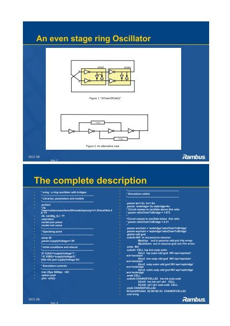
An even stage r<strong>in</strong>g Oscillator<br />
Slide 17<br />
A2<br />
B2<br />
XCell1 XCell2<br />
“bridge”<br />
Figure 1: “XCha<strong>in</strong>OfCells2”<br />
“bridge”<br />
Figure 2: An alternative view<br />
The complete description<br />
• * sr<strong>in</strong>g - a r<strong>in</strong>g oscillator with bridges<br />
• *-----------------------------------------------------------<br />
• * Libraries, parameters <strong>and</strong> models<br />
• *-----------------------------------------------------------<br />
• .protect<br />
• *.lib<br />
'/user/cad/process/tsmc65/model/spice/g+/v1.0/local/fets.li<br />
b' TT<br />
• .lib ./cln90g_lk.l TT<br />
• .unprotect<br />
• .model pch pmos<br />
• .model nch nmos<br />
• *-----------------------------------------------------------<br />
• * Operat<strong>in</strong>g po<strong>in</strong>t<br />
• *-----------------------------------------------------------<br />
• .temp 30<br />
• .param supplyVoltage=1.5V<br />
• *-----------------------------------------------------------<br />
• * Initial conditions <strong>and</strong> stimuli<br />
• *-----------------------------------------------------------<br />
• .IC V(A2)='supplyVoltage*1.'<br />
• *.IC V(B2)='supplyVoltage/2.'<br />
• Vdd vdd gnd supplyVoltage DC<br />
• *-----------------------------------------------------------<br />
• * Simulation controls<br />
• *-----------------------------------------------------------<br />
• .tran 25ps 5000ps UIC<br />
• .option post<br />
• .plot v(A2))<br />
DCC 08<br />
Slide 18<br />
“bridge”<br />
• *-----------------------------------------------------------<br />
• * Simulation netlist<br />
• *-----------------------------------------------------------<br />
• .<br />
• .param lp=1.0u ln=1.0u<br />
• .param wnbridge= 2u wpbridge=4u<br />
• * Circuit ceases to oscillate above this ratio<br />
• *.param ratioCha<strong>in</strong>ToBridge = 1.972<br />
• *<br />
• *Circuit ceases to oscillate below this ratio<br />
• *.param ratioCha<strong>in</strong>ToBridge = 0.31<br />
• *<br />
• .param wncha<strong>in</strong> = 'wnbridge*ratioCha<strong>in</strong>ToBridge'<br />
• .param wpcha<strong>in</strong> = 'wpbridge*ratioCha<strong>in</strong>ToBridge'<br />
• .global vdd gnd<br />
• .subckt INV <strong>in</strong> out psource nsource<br />
• Mpullup out <strong>in</strong> psource vdd pch l=lp w=wp<br />
• Mpulldown out <strong>in</strong> nsource gnd nch l=ln w=wn<br />
• .ends INV<br />
• .subckt CELL <strong>in</strong>p <strong>in</strong>m outp outm<br />
• X<strong>in</strong>v1 <strong>in</strong>p outm vdd gnd INV wp='wpcha<strong>in</strong>'<br />
wn='wncha<strong>in</strong>'<br />
• X<strong>in</strong>v2 <strong>in</strong>m outp vdd gnd INV wp='wpcha<strong>in</strong>'<br />
wn='wncha<strong>in</strong>'<br />
• X<strong>in</strong>v3 outp outm vdd gnd INV wp='wpbridge'<br />
wn='wnbridge'<br />
• X<strong>in</strong>v4 outm outp vdd gnd INV wp='wpbridge'<br />
wn='wnbridge'<br />
• .ends CELL<br />
• .subckt CHAINOFCELLS2 <strong>in</strong>a <strong>in</strong>b outa outb<br />
• XCell1 <strong>in</strong>a <strong>in</strong>b oa1 ob1 CELL<br />
• XCell2 oa1 ob1 outa outb CELL<br />
• .ends CHAINOFCELLS2<br />
• XCha<strong>in</strong>OfCells2 A2 B2 B2 A2 CHAINOFCELLS2<br />
• .end sr<strong>in</strong>g