Programming the MSC1210 (Rev. B) - Texas Instruments
Programming the MSC1210 (Rev. B) - Texas Instruments
Programming the MSC1210 (Rev. B) - Texas Instruments

You also want an ePaper? Increase the reach of your titles
YUMPU automatically turns print PDFs into web optimized ePapers that Google loves.
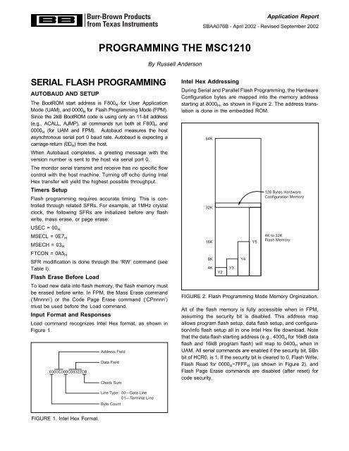
SERIAL FLASH PROGRAMMING<br />
AUTOBAUD AND SETUP<br />
The BootROM start address is F800H for User Application<br />
Mode (UAM), and 0000H for Flash <strong>Programming</strong> Mode (FPM).<br />
Since <strong>the</strong> 2kB BootROM code is using only an 11-bit address<br />
(e.g., ACALL, AJMP), all commands run both at F800H and<br />
0000H (for UAM and FPM). Autobaud measures <strong>the</strong> host<br />
asynchronous serial port 0 baud rate. Autobaud is expecting a<br />
carriage-return (0DH) from <strong>the</strong> host.<br />
When Autobaud completes, a greeting message with <strong>the</strong><br />
version number is sent to <strong>the</strong> host via serial port 0.<br />
The monitor serial transmit and receive has no specific flow<br />
control with <strong>the</strong> host machine. Turning off echo during Intel<br />
Hex transfer will yield <strong>the</strong> highest possible throughput.<br />
Timers Setup<br />
Flash programming requires accurate timing. This is controlled<br />
through related SFRs. For example, at 1MHz crystal<br />
clock, <strong>the</strong> following SFRs are initialized before any flash<br />
write, mass erase, or page erase:<br />
USEC = 00H MSECL = 0E7H MSECH = 03H FTCON = 0A5H SFR modification is done through <strong>the</strong> ‘RW’ command (see<br />
Table I).<br />
Flash Erase Before Load<br />
To load new data into flash memory, <strong>the</strong> flash memory must<br />
be erased before write. In FPM, <strong>the</strong> Mass Erase command<br />
(‘Mnnnn’) or <strong>the</strong> Code Page Erase command (‘CPnnnn’)<br />
must be used before <strong>the</strong> Load command.<br />
Input Format and Responses<br />
Load command recognizes Intel Hex format, as shown in<br />
Figure 1.<br />
:0300C000C08322D8<br />
FIGURE 1. Intel Hex Format.<br />
PROGRAMMING THE <strong>MSC1210</strong><br />
Address Field<br />
Data Field<br />
Check Sum<br />
Line Type: 00—Data Line<br />
01—Terminal Line<br />
Byte Count<br />
By Russell Anderson<br />
Application Report<br />
SBAA076B - April 2002 - <strong>Rev</strong>ised September 2002<br />
Intel Hex Addressing<br />
During Serial and Parallel Flash <strong>Programming</strong>, <strong>the</strong> Hardware<br />
Configuration bytes are mapped into <strong>the</strong> memory address<br />
starting at 8000H, as shown in Figure 2. The address translation<br />
is done in <strong>the</strong> embedded ROM.<br />
64K<br />
32K<br />
16K<br />
8K<br />
4K<br />
Y2<br />
Y3<br />
Y4<br />
FIGURE 2. Flash <strong>Programming</strong> Mode Memory Orginization.<br />
All of <strong>the</strong> flash memory is fully accessible when in FPM,<br />
assuming <strong>the</strong> security bit is disabled. This address map<br />
allows program flash setup, data flash setup, and configuration/info<br />
flash setup all in one Intel Hex file download. Note<br />
that <strong>the</strong> data flash starting address (e.g., 4000 H for 16kB data<br />
flash and 16kB program flash) will map to 0400 H when in<br />
UAM. All serial commands are enabled if <strong>the</strong> security bit, SBn<br />
bit of HCR0, is 1. If <strong>the</strong> security bit is cleared to 0, Flash Write,<br />
Flash Read for 0000 H~7FFF H (as shown in Figure 2), and<br />
Flash Page Erase commands are disabled (after reset) for<br />
code security.<br />
Y5<br />
128 Bytes Hardware<br />
Configuration Memory<br />
4K to 32K<br />
Flash Memory
SERIAL PROGRAMMING AND UAM MONITOR COMMANDS<br />
COMMAND COMMAND NAME RESPONSE PARAMETERS<br />
XRnnnn External Data Read Display: None Read 16 bytes from nnnn (External Data Memory).<br />
XWnnnnyy External Data Write Display: None Write to nnnn (External Data Memory) with yy.<br />
XFnnnnyy Data Flash Write Display: ‘ok’ or ‘x’ for failing Write to nnnn (flash byte data flash memory) with yy.<br />
XPnnnn Data Flash Page Erase Display: ‘ok’ or ‘x’ for failing Erase a 128-byte data flash page.<br />
CRnnnn Code Memory Read Display 16-byte code memory starting from nnnn Read 16 bytes from nnnn (code memory).<br />
CWnnnnyy Code Flash Write Display: ‘ok’ or ‘x’ for failing Write to nnnn (32kB code memory) with yy.<br />
CPnnnn Code Flash Page Erase Display: ‘ok’ or ‘x’ for failing Erase a 128-byte code flash page at nnnn,<br />
lower 7 bits are ignored.<br />
RRnn Register (SFR) Read Display 1-byte SFR at nn Read from nn (128-byte SFR).<br />
RWnnyy Register (SFR) Write Display: None Write to nn (128-byte SFR) with yy.<br />
Fnn PS1 Flash Memory Read Display 16-byte PS1 flash memory starting from nn Read 16 bytes of config/info flash (128-byte PS1<br />
Flash Memory).<br />
Mnnnn Mass Erase Display: ‘ok’ or ‘x’ for failing 0~7FFFFH for PS0 program memory mass erase,<br />
8000H~807FH for PS1 flash memory.<br />
Q Continue Execution from Break Display: None<br />
S Single Step Display: None<br />
E Toggle Echo Display: None<br />
L Load Intel Hex Display: ‘.’ — data line write passes<br />
‘X’ — line write error<br />
‘E’ — line checksum error<br />
‘T’ — termination of transfer<br />
Command is disabled when HCR0.EPMA = 0.<br />
IRnn Internal RAM Read Display: 16-byte IRAM starting from nn (256 bytes RAM) Read 16 bytes from nn (256 bytes of internal RAM).<br />
IWnnyy Internal RAM Write Display: None Write to nn (internal RAM) with yy.<br />
B0nnnnxx Set Breakpoint 0 and Status in BPCON Display: None Write address nnnn to BP0 and status xx to BPCON.<br />
B1nnnnxx Set Breakpoint 1 and Status in BPCON Display: None Write address nnnn to BP1 and status xx to BPCON.<br />
Gnnnn Goto Address Display: None Go to address nnnn.<br />
NOTE: nnn, nn, and yy are hex digits.<br />
TABLE I. Serial <strong>Programming</strong> Command List.<br />
Reset Circuit (or V DD )<br />
1MHz to 24MHz or Crystal<br />
RST<br />
PSEN<br />
ALE<br />
<strong>MSC1210</strong><br />
FIGURE 3. Serial <strong>Programming</strong> and Monitor Configuration.<br />
X IN<br />
Serial<br />
Port 0<br />
P3.1 TXD<br />
P3.0 RXD<br />
RS232<br />
Transceiver<br />
NOTE: Serial programming is selected with PSEN = 0 and ALE = 1 or open.<br />
Host PC<br />
or<br />
Serial Terminal<br />
2 SBAA076B<br />
www.ti.com
PARALLEL FLASH PROGRAMMING<br />
Configuration<br />
When <strong>the</strong> <strong>MSC1210</strong> is configured to parallel programming<br />
mode by pulling PSEN HIGH (or NC) and pulling ALE LOW<br />
while RST is asserted, <strong>the</strong> device ports will be configured for<br />
parallel interface with <strong>the</strong> Host Flash <strong>Programming</strong>, as shown<br />
in Figure 4. Table III shows <strong>the</strong> port definitions. The host will<br />
provide Addr/Cmd/Req/RST/Clk signals, and <strong>the</strong> <strong>MSC1210</strong><br />
will respond with Ack/Pass/Data. The command address<br />
Addr[14:0] is divided into two parts, AddrHi[6:0] and AddrLo[7:0],<br />
i.e. Addr[14:0] = (AddrHi[6:0], AddrLo[7:0]). P3[1:0] are reserved.<br />
and must not be connected (NC).<br />
NC<br />
PSEN<br />
ALE<br />
<strong>MSC1210</strong> HOST<br />
P2[7:0]<br />
P1[7:0]<br />
P0[7:0]<br />
P3[7:5]<br />
P3[4]<br />
P3[3]<br />
P3[2]<br />
RST<br />
XIN<br />
PSEL/AddrHi[6:0]<br />
AddrLo[7:0]<br />
Data[3:0]<br />
Cmd[2:0]<br />
Req<br />
Flash<br />
Programmer<br />
FIGURE 4. Parallel <strong>Programming</strong> Configuration.<br />
FIGURE 5. Parallel <strong>Programming</strong> Handshaking and Timing.<br />
Ack<br />
Pass<br />
RST<br />
CLK<br />
Read Data[7:0]<br />
Write Data[7:0]<br />
PSEL/AddrHi[6:0]<br />
AddrLo[7:0]<br />
Cmd[3:0]<br />
Req<br />
Ack<br />
Pass<br />
RST<br />
t RS<br />
1<br />
Command Handshaking<br />
Figure 5 shows <strong>the</strong> parallel programming sequence starting<br />
from power-on reset. After power-on with PSEN HIGH and<br />
ALE LOW, <strong>the</strong> <strong>MSC1210</strong> is setup for parallel programming;<br />
reference <strong>the</strong> numbers in Figure 5.<br />
(1) Power-On—Ack and Pass signals have internal pull-ups.<br />
Ack and Pass will change to zero when <strong>the</strong> <strong>MSC1210</strong> is<br />
ready to accept new or first commands.<br />
(2) Command Request—After <strong>the</strong> Host detects a LOW on<br />
Ack, <strong>the</strong> host should setup Addr/Dara/Cmd, and raise <strong>the</strong><br />
Req flag. For Host read commands (SFR Read, Flash Read),<br />
<strong>the</strong> host must drive Data with hi-z. For Host write commands,<br />
<strong>the</strong> host must drive Data with command data.<br />
(3) Command Done—After <strong>the</strong> <strong>MSC1210</strong> detects Req, it<br />
executes <strong>the</strong> command, and sets <strong>the</strong> Pass line if <strong>the</strong> command<br />
is successful or clears <strong>the</strong> Pass line if <strong>the</strong> command<br />
fails (e.g. Flash Write Value Check Error). If <strong>the</strong> command is<br />
a read command, it will drive <strong>the</strong> read result on <strong>the</strong> Data bus.<br />
Ack is driven HIGH to acknowledge a command or signal that<br />
<strong>the</strong> command is finished.<br />
(4) Host Acknowledge—The host should detect <strong>the</strong> Ack<br />
signal, drive hi-z to Data for write commands or fetch Data for<br />
read commands, and release <strong>the</strong> Req line to signal <strong>the</strong><br />
<strong>MSC1210</strong> to acknowledge command complete. Setting up a<br />
new Addr and Cmd is optional.<br />
(5) <strong>MSC1210</strong> Acknowledge—After <strong>the</strong> <strong>MSC1210</strong> detects<br />
Req release, Data is driven with hi-z for read commands to<br />
avoid bus conflict, and Ack/Pass is released to prepare for a<br />
new command.<br />
(6) New Command—Procedure repeats from (2) to (5).<br />
SBAA076B 3<br />
www.ti.com<br />
2<br />
t CD<br />
3<br />
t AS<br />
4<br />
t RS<br />
5<br />
6
PORT<br />
DIRECTION<br />
NUMBER PORT NAME FROM TO DESCRIPTION<br />
P2[7] PSEL Host <strong>MSC1210</strong> Host Flash Memory PS0/PS1 Select<br />
P2[6:0] AddrHi[6:0] Host <strong>MSC1210</strong> Host Command Address 14 to 0<br />
P1[7:0] AddrLo[7:0] Host <strong>MSC1210</strong><br />
P0[7:0] Data[7:0] Host <strong>MSC1210</strong> Host Data for Write Commands<br />
<strong>MSC1210</strong> Host <strong>MSC1210</strong> Data for Read Commands<br />
P3[7:5] Cmd[2:0] Host <strong>MSC1210</strong> Host <strong>Programming</strong> Command<br />
P3[4] Req Host <strong>MSC1210</strong> Host Command Request Handshake Line<br />
P3[3] Ack <strong>MSC1210</strong> Host <strong>MSC1210</strong> Command Acknowledge Handshake Line<br />
P3[2] Pass <strong>MSC1210</strong> Host <strong>MSC1210</strong> Command Pass/Fail Line<br />
TABLE III. Parallel <strong>Programming</strong> Port Definitions.<br />
COMMAND DATA BUS<br />
Cmd[2:0] NAME DRIVER DESCRIPTION<br />
000 Flash Read <strong>MSC1210</strong> PSEL = 0 for PS0, PSEL = 1 for PS1, Addr[14:0] is <strong>the</strong> Read Address<br />
001 Flash Write Host PSEL = 0 for PS0, PSEL = 1 for PS1, Addr[14:0] is <strong>the</strong> Write Address<br />
010 Flash Mass Erase None PSEL = 0 for PS0, PSEL = 1 for PS1, Addr[14:0] is Ignored<br />
011 Flash Page Erase None PSEL = 0 for PS0, PSEL = 1 for PS1, Addr[14:7] is <strong>the</strong> Page Address, Addr[6:0] is Ignored<br />
(Page Size is 128 Byte)<br />
100 Reserved None<br />
101 Reserved None<br />
110 SFR Read <strong>MSC1210</strong> PSEL and Addr[14:8] are Ignored, Addr[7:0] is <strong>the</strong> SFR Read Address<br />
111 SFR Write Host PSEL and Addr[14:8] are Ignored, Addr[7:0] is <strong>the</strong> SFR Write Address<br />
TABLE IV. Parallel <strong>Programming</strong> Commands.<br />
PARAMETER DESCRIPTION MIN MAX DESCRIPTION<br />
tRS Req Setup 0µs — Data/Addr/PSEL/Cmd Setup Before Req<br />
tAS Ack Setup 1µs — Data/Pass Setup Before Ack<br />
t (1)<br />
CD Command Delay — 11ms Command Delay for Mass Erase and Page Erase Commands<br />
— 0.5ms Command Delay for Flash Write Commands<br />
— 0.1ms Command Delay for Flash Read/SFR Read/SFR Write Commands<br />
CLK Clock Frequency 1MHz 24MHz System Clock Input.<br />
NOTE: (1) tCD is limited by Flash programming timing, higher CLK will not reduce timing significantly.<br />
TABLE V. Parallel <strong>Programming</strong> Timing.<br />
DIRECTION<br />
Command Timing<br />
<strong>Programming</strong> Setup<br />
Flash programming requires accurate timing. This is controlled<br />
through related SFRs. For example, at 1MHz crystal<br />
clock, <strong>the</strong> following SFRs must be initialized before any Flash<br />
Write, Mass Erase, and Page Erase:<br />
USEC = 00H MSECL = 0e7H MSECH = 03H FTCON = 0a5H SFR modification is done through <strong>the</strong> ‘SFR Write’ command<br />
(see <strong>the</strong> Command Section).<br />
Code Security<br />
All parallel commands, as shown in Table IV, are enabled if <strong>the</strong><br />
security bit, SBn bit of HCR0, is 1. If <strong>the</strong> security bit is cleared<br />
to 0, Flash Write, Flash Read for 0000H~7FFFH (see Figure 2),<br />
and Flash Page Erase commands are disabled (after reset) for<br />
code security. Flash Read for addresses 8000H~807FH for PS1<br />
areas are always enabled, such that <strong>the</strong> manufacturer’s information<br />
and device Flash configuration (HCR0/1) are accessible.<br />
SFR Read and SFR Write are not affected by <strong>the</strong><br />
security bit.<br />
4 SBAA076B<br />
www.ti.com
IMPORTANT NOTICE<br />
<strong>Texas</strong> <strong>Instruments</strong> Incorporated and its subsidiaries (TI) reserve <strong>the</strong> right to make corrections, modifications,<br />
enhancements, improvements, and o<strong>the</strong>r changes to its products and services at any time and to discontinue<br />
any product or service without notice. Customers should obtain <strong>the</strong> latest relevant information before placing<br />
orders and should verify that such information is current and complete. All products are sold subject to TI’s terms<br />
and conditions of sale supplied at <strong>the</strong> time of order acknowledgment.<br />
TI warrants performance of its hardware products to <strong>the</strong> specifications applicable at <strong>the</strong> time of sale in<br />
accordance with TI’s standard warranty. Testing and o<strong>the</strong>r quality control techniques are used to <strong>the</strong> extent TI<br />
deems necessary to support this warranty. Except where mandated by government requirements, testing of all<br />
parameters of each product is not necessarily performed.<br />
TI assumes no liability for applications assistance or customer product design. Customers are responsible for<br />
<strong>the</strong>ir products and applications using TI components. To minimize <strong>the</strong> risks associated with customer products<br />
and applications, customers should provide adequate design and operating safeguards.<br />
TI does not warrant or represent that any license, ei<strong>the</strong>r express or implied, is granted under any TI patent right,<br />
copyright, mask work right, or o<strong>the</strong>r TI intellectual property right relating to any combination, machine, or process<br />
in which TI products or services are used. Information published by TI regarding third–party products or services<br />
does not constitute a license from TI to use such products or services or a warranty or endorsement <strong>the</strong>reof.<br />
Use of such information may require a license from a third party under <strong>the</strong> patents or o<strong>the</strong>r intellectual property<br />
of <strong>the</strong> third party, or a license from TI under <strong>the</strong> patents or o<strong>the</strong>r intellectual property of TI.<br />
Reproduction of information in TI data books or data sheets is permissible only if reproduction is without<br />
alteration and is accompanied by all associated warranties, conditions, limitations, and notices. Reproduction<br />
of this information with alteration is an unfair and deceptive business practice. TI is not responsible or liable for<br />
such altered documentation.<br />
Resale of TI products or services with statements different from or beyond <strong>the</strong> parameters stated by TI for that<br />
product or service voids all express and any implied warranties for <strong>the</strong> associated TI product or service and<br />
is an unfair and deceptive business practice. TI is not responsible or liable for any such statements.<br />
Mailing Address:<br />
<strong>Texas</strong> <strong>Instruments</strong><br />
Post Office Box 655303<br />
Dallas, <strong>Texas</strong> 75265<br />
Copyright © 2002, <strong>Texas</strong> <strong>Instruments</strong> Incorporated