
You also want an ePaper? Increase the reach of your titles
YUMPU automatically turns print PDFs into web optimized ePapers that Google loves.
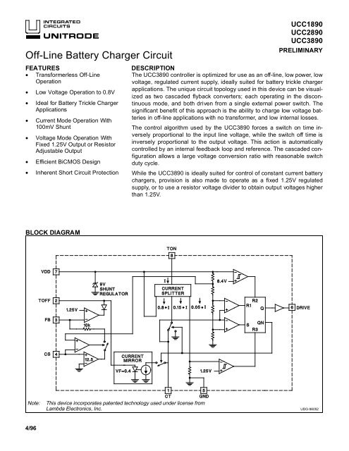
<strong>Off</strong>-<strong>Line</strong> <strong>Battery</strong> <strong>Charger</strong> <strong>Circuit</strong><br />
FEATURES<br />
• Transformerless <strong>Off</strong>-<strong>Line</strong><br />
Operation<br />
• Low Voltage Operation to 0.8V<br />
• Ideal for <strong>Battery</strong> Trickle <strong>Charger</strong><br />
Applications<br />
• Current Mode Operation With<br />
100mV Shunt<br />
• Voltage Mode Operation With<br />
Fixed 1.25V Output or Resistor<br />
Adjustable Output<br />
• Efficient BiCMOS Design<br />
• Inherent Short <strong>Circuit</strong> Protection<br />
BLOCK DIAGRAM<br />
Note: This device incorporates patented technology used under license from<br />
Lambda Electronics, Inc.<br />
4/96<br />
UCC1890<br />
UCC2890<br />
UCC3890<br />
PRELIMINARY<br />
DESCRIPTION<br />
The UCC3890 controller is optimized for use as an off-line, low power, low<br />
voltage, regulated current supply, ideally suited for battery trickle charger<br />
applications. The unique circuit topology used in this device can be visualized<br />
as two cascaded flyback converters; each operating in the discontinuous<br />
mode, and both driven from a single external power switch. The<br />
significant benefit of this approach is the ability to charge low voltage batteries<br />
in off-line applications with no transformer, and low internal losses.<br />
The control algorithm used by the UCC3890 forces a switch on time inversely<br />
proportional to the input line voltage, while the switch off time is<br />
inversely proportional to the output voltage. This action is automatically<br />
controlled by an internal feedback loop and reference. The cascaded configuration<br />
allows a large voltage conversion ratio with reasonable switch<br />
duty cycle.<br />
While the UCC3890 is ideally suited for control of constant current battery<br />
chargers, provision is also made to operate as a fixed 1.25V regulated<br />
supply, or to use a resistor voltage divider to obtain output voltages higher<br />
than 1.25V.<br />
UDG-96052
ABSOLUTE MAXIMUM RATINGS<br />
IDD . . . . . . . . . . . . . . . . . . . . . . . . . . . . . . . . . . . . . . . . . . 7.5mA<br />
Current into TON . . . . . . . . . . . . . . . . . . . . . . . . . . . . . . . 7.5mA<br />
Voltage on VOUT . . . . . . . . . . . . . . . . . . . . . . . . . . . . . . . . . . . . . . . . . . . 20V<br />
Current into TOFF . . . . . . . . . . . . . . . . . . . . . . . . . . . . . . 250μA<br />
Storage Temperature . . . . . . . . . . . . . . . . . . . –65°C to +150°C<br />
Junction Temperature . . . . . . . . . . . . . . . . . . –55°C to +150°C<br />
Lead Temperature (Soldering, 10 sec.) . . . . . . . . . . . . . +300°C<br />
Currents are positive into, negative out of the specified terminal.<br />
Consult Packaging Section of Databook for thermal limitations<br />
and considerations of packages.<br />
CONNECTION DIAGRAMS<br />
DIL-8, SOIC-8 (Top View)<br />
J, N, or D Packages<br />
ELECTRICAL CHARACTERISTICS: Unless otherwise stated, these specifications apply for TA = –55°C to 125°C for<br />
UCC1890, –40°C to 85°C for the UCC2890, and 0°C to 70°C for the UCC3890. No load at DRIVE pin (CLOAD = 0), TA = TJ.<br />
UCC1890<br />
UCC2890<br />
UCC3890<br />
PARAMETER TEST CONDITIONS MIN TYP MAX UNITS<br />
General<br />
VDD Zener Voltage ITON = 4.75mA 8.7 9.0 9.3 V<br />
Operating Current ITON<br />
Undervoltage Lockout<br />
IDD = –1mA, F = 150kHz 2 mA<br />
Minimum Voltage to Start 8.0 8.4 8.9 V<br />
Minimum Voltage after Start 5.8 6.2 6.6 V<br />
Hysteresis<br />
Oscillator<br />
1.8 V<br />
Amplitude ITON = 3mA; ITOFF = 50μA; VFB = 0V CT = 100pF 3.1 3.4 3.7 V<br />
CT to DRIVE High Delay Overdrive = 200mV 100 200 ns<br />
CT to DRIVE Low Delay Overdrive = 200mV 50 100 ns<br />
Charge Coefficient ICT/ITON ITON = 3mA; VCT = 3.0V 0.135 0.15 0.165 μA/μA<br />
Discharge Coefficent ICT/ITOFF<br />
Driver<br />
ITOFF = 50μA; VCT = 3.0V 0.95 1.00 1.05 μA/μA<br />
VOL I = 100mA (Note 1) 0.7 1.8 V<br />
VOH I = –100mA referred to VDD (Note 1) –2.9 –1.2 V<br />
Rise Time CL = 1nF 35 70 ns<br />
Fall Time<br />
<strong>Line</strong> Voltage Detection<br />
CL = 1nF 30 60 ns<br />
Minimum ITON for Fault 1.0 1.5 2.0 mA<br />
ITON Detector Hysteresis 80 μA<br />
On Time During Fault<br />
VOUT Error Amplifier<br />
2 μs<br />
Reference Level ITOFF = 50μA, ICT = 25μA 1.20 1.25 1.30 V<br />
Voltage at TOFF ITOFF = 50μA 0.3 0.4 0.5 V<br />
Regulation gm<br />
Current Sense Amplifier<br />
ITOFF = 50μA (Note 2) 2.25 4.5 6.75 mA/V<br />
Gain VCS = 90 – 110mV 11.8 12.5 13.0 V/V<br />
Input <strong>Off</strong>set Voltage VCS = 90 – 110mV –5 0 5 mV<br />
Input Voltage for CS Amplifier Enabled ITON = 3mA, Referred to VDD –1.5 –0.8 V<br />
Input Voltage for CS Amplifier Disabled ITON = 3mA, Referred to VDD –0.8 –0.3 V<br />
CS Amplifier Source Impedance 5 10 15 kΩ<br />
Note 1: VDD forced to 100mV below VDD Zener Voltage<br />
Note 2: gm is defined as ΔICT<br />
for the values of VFB where the error amp is in regulation. The two points used to calculate gm<br />
ΔVFB<br />
are for ICT at 65% amd 35% of its maximum value.<br />
2
PIN DESCRIPTIONS<br />
CS: The high side of the current sense shunt is connected<br />
to this pin. Short CS to VDD for voltage feedback<br />
operation.<br />
CT: Oscillator timing capacitor is connected to this pin.<br />
DRIVE: Gate drive to external power switch.<br />
FB: Output of current sense amplifier. This pin can be<br />
used for direct output voltage feedback if the current<br />
sense amp input pin CS is shorted to the VDD pin.<br />
GND: Ground pin.<br />
APPLICATION INFORMATION<br />
OPERATION (VOLTAGE OUTPUT)<br />
Figure 1 shows a typical voltage mode application.<br />
When input voltage is first applied, all of the current<br />
through RDD and 80% of the current through RON,<br />
charge the external capacitor C3 connected to VDD. As<br />
the voltage builds on VDD, undervoltage lockout holds<br />
the circuit off and the output DRIVE low until VDD<br />
reaches 8.4V. At this time, DRIVE goes high, turning on<br />
the external power switch Q1, and 15% of the current<br />
into TON is directed to the timing capacitor CT. The voltage<br />
at TON is fixed at approximately 11V, so CT<br />
charges to a fixed threshold with current<br />
VIN – 11V<br />
I = 0.2 •<br />
RON<br />
Since the input line is much greater than 11V, the<br />
charge current is approximately proportional to the input<br />
line voltage. DRIVE is only high while CT is charging, so<br />
Figure 1. Typical Voltage Mode Application<br />
3<br />
UCC1890<br />
UCC2890<br />
UCC3890<br />
TOFF: Resistor ROFF connects from voltage output to<br />
this pin to provide a maximum capacitor discharge current<br />
proportional to output voltage.<br />
TON: Resistor RON connects from line input to this pin to<br />
provide capacitor charge current proportional to line voltage.<br />
The current in RON also provides power for the 9V<br />
shunt regulator at VDD.<br />
VDD: Output of 9V shunt regulator.<br />
UDG-96053<br />
the power switch on time is inversely proportional to line<br />
voltage. This provides a constant line voltage-switch on<br />
time product.<br />
At the end of the switch on time, Q1 is turned off, and<br />
the 15% of the RON current which was charging CT is<br />
diverted to ground. The power switch off time is controlled<br />
by discharge of CT, which is determined by the outut<br />
voltage as described here:<br />
UDG-96054
APPLICATION INFORMATION (cont.)<br />
1. When VOUT = 0, the off time is infinite. This feature<br />
provides inherent short circuit protection. However,<br />
to ensure output voltage startup when the output is<br />
not a short, a high value resistor, RS, is placed in<br />
parallel with CT to establish a minimum switching<br />
frequency.<br />
2. As VOUT rises above approximately 0.4V, IDCHG is<br />
set by ROFF, and is defined by<br />
VOUT – 0.4V<br />
IDCHG =<br />
ROFF<br />
As VOUT increases, IDCHG increases resulting in the<br />
reduction of off time. The frequency of operation increases<br />
and VOUT rises quickly to its regulated<br />
value.<br />
3. In this region, a transconductance amplifier reduces<br />
IDCHG in order to maintain VOUT in regulation. The<br />
input to the transconductance amplifier is the pin FB.<br />
(In this mode the pin CS should be shorted to VDD.)<br />
FB can either be connected directly to VOUT to regulate<br />
at nominal VOUT = 1.25V or to be connected to<br />
VOUT through a resistor divider RVS1/RVS2 to regulate<br />
at nominal<br />
VOUT =<br />
1.25V • (RVS1 + RVS2)<br />
RVS2<br />
4. If VOUT should rise above its regulation range, IDCHG<br />
falls to zero and the circuit returns to the minimum<br />
frequency established by RS and CT.<br />
The range of switching frequencies is established by<br />
RON, ROFF, RS, and CT as follows:<br />
Frequency =<br />
TON =<br />
Figure 2. Typical Current Mode Application<br />
4<br />
1<br />
TON + TOFF<br />
CT • 3.4V • 0.15 • RON<br />
VIN – 11V<br />
UCC1890<br />
UCC2890<br />
UCC3890<br />
TOFF(MAX) = 1.5 • RS • CT (regions 1 and 4)<br />
CT • 3.4V • ROFF<br />
TOFF = (region 2)<br />
VOUT − 0.4V<br />
The above equations assume VDD = 9, the voltage<br />
at TON = 11V, the voltage at TOFF = 0.4V.<br />
OPERATION (CURRENT OUTPUT)<br />
Figure 2 shows a typical current mode application. In<br />
current mode, operation is the same as in voltage<br />
mode, except that in region 3 the transconductance amplifier<br />
is controlled by the current sense amplifier which<br />
senses the voltage across a shunt resistor RSH. The circuit<br />
then regulates the current in the shunt to the nominal<br />
value<br />
ISH = 100mV<br />
RSH<br />
The circuit shown in this schematic would be suitable<br />
for an application which trickle charges a battery at a<br />
low current, (e.g. C/10), and has a battery load which<br />
draws a high current, (e.g. C), when turned on. In that<br />
case, RSH1 value is chosen so that<br />
100mV C<br />
=<br />
RSH1 10<br />
UDG-96055
APPLICATION INFORMATION (cont.)<br />
If RSH2 is chosen so that<br />
100mV<br />
= C<br />
RSH2<br />
then the regulator output will assist the battery, minimizing<br />
or eliminating battery output current.<br />
DESIGN EXAMPLE<br />
A typical design has the following requirements:<br />
VIN = 80 to 132 VAC or 100 to 180 VDC<br />
VOUT = 1.25V<br />
VOUT′ = 2.0V (assumes 1.25 VOUT with<br />
750mV forward drop in D3)<br />
ILOAD = 500mADC max<br />
FSWITCHING= 100kHz<br />
η (eff.) = 50% (excluding efficiency losses in<br />
D3 which will be very large due to the<br />
low output voltage. Losses in D3 are<br />
accounted for by using VOUT′ in the<br />
calculations).<br />
Component values are indicated in Figure 3. The explanation<br />
for the choices in component values follows.<br />
First calculate the maximum duty cycle, d(max). To calculate<br />
this assume that at maximum load/minimum line<br />
conditions, the converter will be at the continuous conduction<br />
boundary and there will be no idle time after the<br />
inductors are discharged. For all other load/line conditions,<br />
the UCC3890 will stretch the off time, to create an<br />
idle time after the inductors are discharged, in order to<br />
UCC1890<br />
UCC2890<br />
UCC3890<br />
maintain a constant output voltage. For a single flyback<br />
stage at continuous conduction boundary<br />
1<br />
d =<br />
1 + VIN<br />
VOUT<br />
For the cascaded flyback stages of the UCC3890 topology,<br />
the corresponding equation is<br />
d(max) =<br />
in this case<br />
1<br />
1 + √⎺⎺⎺ VIN<br />
VOUT′<br />
1<br />
d(max) =<br />
1 + √⎺⎺⎺ 100V<br />
2V<br />
= 0.125<br />
Next using the operating frequency and the maximum<br />
duty cycle to calculate the maximum on time<br />
TON(max) = d(max)<br />
FSWITCHING<br />
in this case<br />
TON(max) = 0.125<br />
= 1.25μs<br />
100kHz<br />
correspondingly<br />
TOFF(min) =<br />
Figure 3. Example Application<br />
5<br />
1 − 0.125<br />
100kHz<br />
= 8.75μs<br />
UDG-96056
APPLICATION INFORMATION (cont.)<br />
The average input current at minimum line and maximum<br />
load will be<br />
IIN = IOUT<br />
η<br />
in this case<br />
IIN = 500mA<br />
0.5<br />
• VOUT′<br />
VIN<br />
2V<br />
• = 20mA<br />
100V<br />
Knowing that input current is drawn from the line only<br />
during TON, calculate the peak current in L1 to be<br />
IL1(pk) = 2 • IIN •<br />
in this case<br />
TON + TOFF<br />
TON<br />
1.25μs + 8.75μs<br />
IL1(pk) = 2 • 20mA •<br />
1.25μs<br />
Now calculate the value for L1<br />
L1 = VIN • TON<br />
IL1(pk)<br />
in this case<br />
= 320mA<br />
L1 = 100V • 1.25μs<br />
= 390μH<br />
320mA<br />
The output voltage of the first flyback stage is<br />
VC1 = VIN • TON<br />
TOFF<br />
in this case<br />
VC1 = 100V • 1.25μs<br />
= 14.3V<br />
8.75μs<br />
Knowing that output current is provided to the load only<br />
during TOFF, calculate the peak current in L2 to be<br />
IL2(pk) = 2 • IOUT •<br />
in this case<br />
IL2(pk) = 2 • 0.5A •<br />
TON + TOFF<br />
TOFF<br />
Now calculate the value of L2<br />
L2 = VOUT′ • TOFF<br />
IL2(pk)<br />
in this case<br />
1.25μs + 8.75μs<br />
8.75μs<br />
= 1.14A<br />
L2 = 2V • 8.75μs<br />
= 15μH<br />
1.14A<br />
For all of the calculations so far only the maximum<br />
load/minimum line condition have been considered. The<br />
6<br />
entire range of operation must be considered to choose<br />
values for the rest of the components.<br />
Under all normal operating conditions the current ITON,<br />
(which is the current in RON), should be greater than<br />
2mA and less than 7.5mA. In this case set RON to give<br />
ITON = 2.8mA at low line. The voltage at TON will be<br />
about 11V so<br />
100V − 11V<br />
RON = = 33kΩ<br />
2.8mA<br />
With RON = 33k, ITON at high line will be<br />
180V − 11V<br />
ITON = = 5.1mA<br />
33k<br />
At high line, the power dissipation in RON will be<br />
P(RON) = (180V − 11V) • 5.1mA = 860mW<br />
RON will need to be at least a 1W resistor. Alternately it<br />
could be four 1/4W 8.2kΩ resistors in series.<br />
Once RON is set, CT can be chosen. The charge current<br />
for CT is nominally 15% of ITON, and the nominal oscillator<br />
amplitude is 3.4V, so<br />
CT • 3.4V<br />
TON =<br />
0.15 • ITON<br />
solving for CT<br />
TON • 0.15 • ITON<br />
CT =<br />
3.4V<br />
ITON at low line is 2.8mA, and the target TON at low line<br />
is 1.25μs, so in this case<br />
1.25μs • 0.15 • 2.8mA<br />
CT = = 150pF<br />
3.4V<br />
The final component to be chosen is ROFF, which determines<br />
the minimum value of TOFF. When the output<br />
voltage is below the regulation point, the discharge current<br />
for CT is equal to ITOFF (the current in ROFF). Under<br />
that condition<br />
CT • 3.4V<br />
TOFF =<br />
ITOFF<br />
since the voltage at the TOFF pin = 0.4V<br />
VOUT − 0.4V<br />
ITOFF =<br />
ROFF<br />
substituting and solving for ROFF<br />
ROFF =<br />
TOFF • (VOUT − 0.4V)<br />
CT • 3.4V<br />
UCC1890<br />
UCC2890<br />
UCC3890<br />
The largest discharge current, and hence the minimum<br />
off time, will occur when the output is about 10mV be-
APPLICATION INFORMATION (cont.)<br />
low the regulation point of 1.25V. The minimum value<br />
for TOFF is 8.75μs. So in this case<br />
8.75μs • (1.24V − 0.4V)<br />
ROFF = = 15k<br />
150pF • 3.4V<br />
OTHER APPLICATION CONSIDERATIONS<br />
Output Capacitor: For best regulation of the output<br />
voltage or current, the output capacitor should be a low<br />
ESR type. This is especially true when operating in current<br />
sense mode with a non-linear load such as a battery.<br />
If a low ESR capacitor cannot be used, excellent<br />
regulation can also be achieved by placing a low pass<br />
R/C filter between the current shunt and the CS input.<br />
No Load Operation: The UCC3890 is inherently protected<br />
for short circuits, but not for open circuits. If the<br />
load is removed, the output voltage will quickly rise up<br />
to the regulation point. Once the output is above the<br />
regulation voltage, the oscillator will drop to the minimum<br />
frequency set by RS/CT. With no load on the output,<br />
even at this low frequency the output voltage can<br />
quickly rise to a dangerous level. To protect against this,<br />
it is recommended that a zener or other voltage clamp<br />
always be connected across the output. The clamp<br />
should be chosen to be above the normal range of output<br />
voltage, but low enough to protect the output capacitor.<br />
In current sense operation, removal of the load<br />
will also break the regulation loop, in which case a sim-<br />
UNITRODE INTEGRATED CIRCUITS<br />
7 CONTINENTAL BLVD. • MERRIMACK, NH 03054<br />
TEL. (603) 424-2410 • FAX (603) 424-3460<br />
7<br />
UCC1890<br />
UCC2890<br />
UCC3890<br />
ple clamp on the output may not be adequate. In current<br />
sense mode it is recommended that a second zener be<br />
connected from the output to the FB pin, the breakdown<br />
voltage of this clamp chosen to be high enough so that<br />
it will not conduct during normal operation, but will conduct<br />
at least 2V lower than the breakdown voltage of<br />
the other clamp.<br />
Gate Drive for the External FET: The UCC3890 is<br />
guaranteed to be able to deliver at least 1mA of steady<br />
state current to the gate of the external FET at ITON =<br />
2mA. If ITON is higher than 2mA, 80% of the additional<br />
current is available to drive the FET gate. If, as in the<br />
design example above, a moderate sized FET such as<br />
the IRF820 is used, the operating frequency is 100kHz,<br />
and the minimum ITON at low line is 2.8mA, then the<br />
available gate drive current may be adequate. The<br />
IRF820 needs about 13nC to charge the gate on each<br />
cycle. At 100kHz, this is equivalent to 1.3mA steady<br />
state; below the minimum 1.64mA available. In some<br />
combinations of a larger FET, and/or higher frequency<br />
operation, the current available for driving the gate may<br />
not be adequate. In that case extra current may be provided<br />
by connecting a resistor RDD from the line input to<br />
the VDD pin. This resistor should be sized so that under<br />
all conditions the current input to VDD is below the<br />
7.5mA absolute maximum limit. RDD will likely need to<br />
be a power resistor.
7 CONTINENTAL BLVD. • MERRIMACK, NH 03054 • TEL (603) 424-2410 • FAX (603) 424-3460