Lecture 15: XRD and Other Analytical Techniques X-Ray Diffraction ...
Lecture 15: XRD and Other Analytical Techniques X-Ray Diffraction ...
Lecture 15: XRD and Other Analytical Techniques X-Ray Diffraction ...

You also want an ePaper? Increase the reach of your titles
YUMPU automatically turns print PDFs into web optimized ePapers that Google loves.
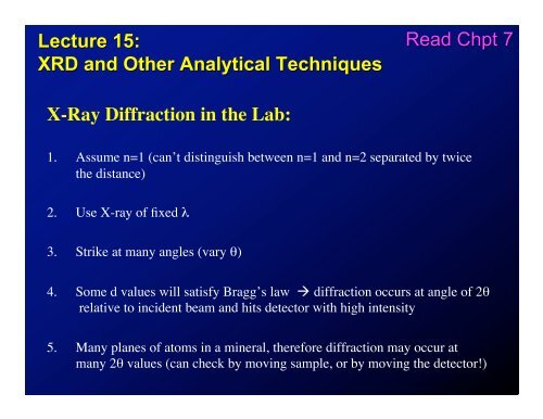
<strong>Lecture</strong> <strong>15</strong>:<br />
<strong>XRD</strong> <strong>and</strong> <strong>Other</strong> <strong>Analytical</strong> <strong>Techniques</strong><br />
Read Chpt 7<br />
X-<strong>Ray</strong> <strong>Diffraction</strong> in the Lab:<br />
1. Assume n=1 (can’t distinguish between n=1 <strong>and</strong> n=2 separated by twice<br />
the distance)<br />
2. Use X-ray of fixed !<br />
3. Strike at many angles (vary ")<br />
4. Some d values will satisfy Bragg’s law ! diffraction occurs at angle of 2"<br />
relative to incident beam <strong>and</strong> hits detector with high intensity<br />
5. Many planes of atoms in a mineral, therefore diffraction may occur at<br />
many 2" values (can check by moving sample, or by moving the detector!)
We can write {hkl} for any planes, does that mean that there will be<br />
infinitely many solutions to Bragg’s Law?<br />
NO! We only get diffraction along planes of high atomic<br />
density that aren’t effect by EXTINCTIONS<br />
Example:<br />
a<br />
d 210<br />
d 010<br />
d 020<br />
d 100<br />
d 200<br />
b<br />
b=5Å<br />
a = 3Å<br />
Which d hkl spacings will give intense diffraction peaks??
d 010 = 6Å ?<br />
lots of atoms => intense diffraction<br />
peaks<br />
d 010<br />
d 020<br />
d 020 = 3Å ?<br />
No atoms on every other => peak occurs though,<br />
because n=2 with d 020 is just like d 010 (less<br />
intense than d 010 peak)
d 200 = 2Å ?<br />
lots of atoms => intense diffraction<br />
peaks<br />
d 200<br />
d 100 = 4Å ?<br />
no diffraction (EXTINCTION)<br />
d 100
Extinctions: due to destructive interference, one plane of atoms<br />
‘cancels’ diffraction from another plane<br />
Note: End-centered, Body-centered unit cells will result in extinctions
Higher symmetry minerals<br />
will have fewer, but more<br />
intense diffraction peaks
2 Types of <strong>XRD</strong>:<br />
(1) Single Crystal:<br />
Laue Technique: orient crystal with axes perp. or parallel to X-ray beam,<br />
put film behind crystal, record spots<br />
Modern single crystal: rotate crystal <strong>and</strong>/or detector<br />
Crystal structure determination: chemical composition <strong>and</strong> single<br />
crystal diffraction patterns allows complete structure to be<br />
determined
2 Types of <strong>XRD</strong>:<br />
(2) Powder <strong>Diffraction</strong>: X-ray finely powdered samples; r<strong>and</strong>om<br />
orientation ensure that all {hkl} planes will satisfy Bragg’s Law<br />
Ex. d 111 = 5Å {111} has high density<br />
n=1; d 111 = 5Å; CuK# = 1.54Å<br />
Then:<br />
n ! = 2d sin "<br />
(1) (1.54Å)/(2)(5Å) = sin "<br />
" = 17.74°<br />
Therefore, grains oriented at " = 17.74° will give strong diffraction peak<br />
In practice: measure " <strong>and</strong> intensity<br />
Calculate d hkl
Peak intensity reflects:<br />
1. density of atoms on {hkl} planes<br />
2. types of atoms on {hkl} planes<br />
X-<strong>Ray</strong> Powder <strong>Diffraction</strong> File:<br />
1. Assign most intense peak 100%<br />
2. Index peaks (assign d-values)<br />
3. Look up d values/relative intensities<br />
A Pain!!! Intensities depend on sample prep, purity (solid solution)…
(1) X <strong>Ray</strong> Fluorescence Spectroscopy<br />
“bulk technique”<br />
sample prep = grind sample to powder, make pressed pellet<br />
Method:<br />
• irradiate sample with high energy X-rays<br />
• some electrons knock out inner shell electrons; outer shell electrons fall <strong>and</strong><br />
emit characteristic wavelength secondary X-rays<br />
• intensity of characteristic spectrum relates to quantity; samples with many<br />
elements will result in many spectral line emissions
(2) Electron Microscope<br />
"! use electrons rather than visible light<br />
"! Why? Better resolution; theoretical limit = ~1/2 ! radiation (e.g., 3000Å<br />
for light microscope)<br />
"! Concept: collimate <strong>and</strong> focus an electron beam using magnetic coils<br />
(analogous to optical lens in a light microscope); resolving power<br />
now:
a. Electron Microprobe (EM)<br />
•! electrons excite inner electrons to produce secondary X-rays, measure just like<br />
in XRF<br />
•! spot size: ~1micron (10000 Å)<br />
•! sample prep: polished thin section<br />
•! Advantage: quantitative chemical analyses can be made over very small areas<br />
(e.g., study exsolution lamellae); relatively nondestructive, quick
. Scanning Electron Microscope (SEM)<br />
•! bombard specifment with rastering electron beam<br />
•! secondary electrons (emitted from speciment) + backscattered electrons (interact<br />
with specimen <strong>and</strong> reflect out) result<br />
•! collect emitted current, amplify <strong>and</strong> display as trace on cathode tube (fluorescent<br />
screen)<br />
•! result: very high magnification topography (like light microscope) with either<br />
secondary or backscattered electrons (heavy atoms = more scattering = darker<br />
image); emitted secondary x-rays can also be collected <strong>and</strong> used for chemical<br />
analysis
c. Transmission Electron Microscope<br />
! much like SEM, but now can get resolution ~1.5Å!!; not quite<br />
individual atoms<br />
n" = 2d hkl sin#<br />
!
(3) Atomic Force Microscopy<br />
"! mount a very small tip (usually triangle 100-200micron long,<br />
5 micron thick) at the end of a cantilever<br />
"! drag it back <strong>and</strong> forth over sample, measure deflection with a<br />
laser, yields topography at Å resolution in air or water,<br />
on insulators or conductors (some tip artifacts)<br />
"! used to study adsorbed atoms, mineral dissolution <strong>and</strong> growth<br />
processes
Scanning Tunnelling Microscopy (STM)<br />
!<br />
* look at electronic structure of surface<br />
* position tip over point, ramp voltage<br />
* negative sample bias: electrons tunnel from sample to tip<br />
* measure tunneling current<br />
* can’t be used on insulators