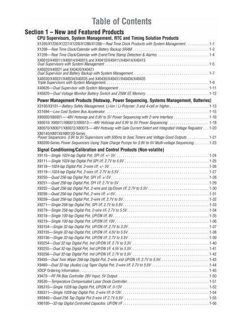
Table of Contents Section 1 – New and Featured Products
Table of Contents Section 1 – New and Featured Products
Table of Contents Section 1 – New and Featured Products

Create successful ePaper yourself
Turn your PDF publications into a flip-book with our unique Google optimized e-Paper software.
<strong>Table</strong> <strong>of</strong> <strong>Contents</strong><br />
<strong>Section</strong> 1 <strong>–</strong> <strong>New</strong> <strong>and</strong> <strong>Featured</strong> <strong>Products</strong><br />
CPU Supervisors, System Management, RTC <strong>and</strong> Timing Solution <strong>Products</strong><br />
X1205/X1226/X1227/X1228/X1286/X1288—Real Time Clock <strong>Products</strong> with System Management . . . . . . . . . . . . 1-1<br />
X1208—Real Time Clock/Calendar with Battery Backup SRAM . . . . . . . . . . . . . . . . . . . . . . . . . . . . . . . . . . . . . . . 1-3<br />
X1209—Real Time Clock/Calendar with Event/Time Stamp Detection & Alarms . . . . . . . . . . . . . . . . . . . . . . . . . . 1-4<br />
X40010/X40011/X40014/X40015 <strong>and</strong> X40410/X40411/X40414/X40415<br />
Dual Supervisors with System Management . . . . . . . . . . . . . . . . . . . . . . . . . . . . . . . . . . . . . . . . . . . . . . . . . . . . . 1-5<br />
X40020/X40021 <strong>and</strong> X40420/X40421<br />
Dual Supervisor <strong>and</strong> Battery Backup with System Management. . . . . . . . . . . . . . . . . . . . . . . . . . . . . . . . . . . . . . . 1-7<br />
X40030/X40031/X40034/X40035 <strong>and</strong> X40430/X40431/X40434/X40435<br />
Triple Supervisors with System Management. . . . . . . . . . . . . . . . . . . . . . . . . . . . . . . . . . . . . . . . . . . . . . . . . . . . . 1-9<br />
X40626—Dual Supervisor with System Management . . . . . . . . . . . . . . . . . . . . . . . . . . . . . . . . . . . . . . . . . . . . . . 1-11<br />
X45620—Dual Voltage Monitor Battery Switch <strong>and</strong> 256K EE Memory . . . . . . . . . . . . . . . . . . . . . . . . . . . . . . . . 1-12<br />
Power Management <strong>Products</strong> [Hotswap, Power Sequencing, Systems Management, Batteries]<br />
X3100/X3101—Battery Safety Management. Li-Ion / Li-Polymer: 3 <strong>and</strong> 4-cell or higher. . . . . . . . . . . . . . . . . . . . . 1-13<br />
X51694—Low Cost System Bus Accelerator . . . . . . . . . . . . . . . . . . . . . . . . . . . . . . . . . . . . . . . . . . . . . . . . . . . . . 1-15<br />
X80000/X80001—-48V Hotswap <strong>and</strong> 0.9V to 5V Power Sequencing with 2-wire Interface . . . . . . . . . . . . . . . . . . 1-16<br />
X80010/ X80011/X80012/X80013—-48V Hotswap <strong>and</strong> 0.9V to 5V Power Sequencing . . . . . . . . . . . . . . . . . . . . 1-18<br />
X80070/X80071/X80072/X80073—-48V Hotswap with Gate Current Select <strong>and</strong> Integrated Voltage Regulator . . . 1-20<br />
X80140/X80130/X80120-Series<br />
Power Sequencers. 0.9V to 5V Supervisors with 500ms to 5sec Timers <strong>and</strong> Voltage Good Outputs . . . . . . . . . . . 1-21<br />
X80200-Series Power Sequencers Using Triple Charge Pumps for 0.9V to 5V Multi-voltage Sequencing. . . . . . . . 1-23<br />
Signal Conditioning/Calibration <strong>and</strong> Control <strong>Products</strong> (Non-volatile)<br />
X9110—Single 1024-tap Digital Pot, SPI I/F, +/- 5V. . . . . . . . . . . . . . . . . . . . . . . . . . . . . . . . . . . . . . . . . . . . . . . . 1-24<br />
X9111—Single 1024-tap Digital Pot SPI I/F, 2.7V to 5.5V . . . . . . . . . . . . . . . . . . . . . . . . . . . . . . . . . . . . . . . . . . . 1-25<br />
X9118—1024-tap Digital Pot, 2-wire I/F, +/- 5V. . . . . . . . . . . . . . . . . . . . . . . . . . . . . . . . . . . . . . . . . . . . . . . . . . . 1-26<br />
X9119—1024-tap Digital Pot, 2-wire I/F, 2.7V to 5.5V . . . . . . . . . . . . . . . . . . . . . . . . . . . . . . . . . . . . . . . . . . . . . . 1-27<br />
X9250—Quad 256-tap Digital Pot, SPI I/F, +/-5V . . . . . . . . . . . . . . . . . . . . . . . . . . . . . . . . . . . . . . . . . . . . . . . . . . 1-28<br />
X9251—Quad 256-tap Digital Pot, SPI I/F, 2.7V to 5V . . . . . . . . . . . . . . . . . . . . . . . . . . . . . . . . . . . . . . . . . . . . . . 1-29<br />
X9252—Quad 256-tap Digital Pot, 2-wire <strong>and</strong> Up/Down I/F, 2.7V to 5.5V . . . . . . . . . . . . . . . . . . . . . . . . . . . . . . . 1-30<br />
X9258—Quad 256-tap Digital Pot, 2-wire I/F, +/-5V. . . . . . . . . . . . . . . . . . . . . . . . . . . . . . . . . . . . . . . . . . . . . . . . 1-31<br />
X9259—Quad 256-tap Digital Pot, 2-wire I/F, 2.7V to 5V . . . . . . . . . . . . . . . . . . . . . . . . . . . . . . . . . . . . . . . . . . . . 1-32<br />
X9271—Single 256-tap Digital Pot, SPI I/F, 2.7V to 5.5V. . . . . . . . . . . . . . . . . . . . . . . . . . . . . . . . . . . . . . . . . . . . 1-33<br />
X9279—Single 256-tap Digital Pot, 2-wire I/F, 2.7V to 5.5V. . . . . . . . . . . . . . . . . . . . . . . . . . . . . . . . . . . . . . . . . . 1-34<br />
X9318—Single 100-tap Digital Pot, UP/DN I/F, 8V . . . . . . . . . . . . . . . . . . . . . . . . . . . . . . . . . . . . . . . . . . . . . . . . . 1-35<br />
X9319—Single 100-tap Digital Pot, UP/DN I/F, 10V . . . . . . . . . . . . . . . . . . . . . . . . . . . . . . . . . . . . . . . . . . . . . . . . 1-36<br />
X93154—Single 32-tap Digital Pot, UP/DN I/F, 2.7V to 3.3V . . . . . . . . . . . . . . . . . . . . . . . . . . . . . . . . . . . . . . . . . 1-37<br />
X93155—Single 32-tap Digital Pot, UP/DN I/F, 4.5V to 5.5V . . . . . . . . . . . . . . . . . . . . . . . . . . . . . . . . . . . . . . . . . 1-38<br />
X93156—Single 32-tap Digital Pot, UP/DN I/F, 2.7V to 5.5V . . . . . . . . . . . . . . . . . . . . . . . . . . . . . . . . . . . . . . . . . 1-39<br />
X93254—Dual 32-tap Digital Pot, Ind UP/DN I/F, 2.7V to 3.3V . . . . . . . . . . . . . . . . . . . . . . . . . . . . . . . . . . . . . . . 1-40<br />
X93255—Dual 32-tap Digital Pot, Ind UP/DN I/F, 4.5V to 5.5V . . . . . . . . . . . . . . . . . . . . . . . . . . . . . . . . . . . . . . . 1-41<br />
X93256—Dual 32-tap Digital Pot, Ind UP/DN I/F, 2.7V to 5.5V . . . . . . . . . . . . . . . . . . . . . . . . . . . . . . . . . . . . . . . 1-42<br />
X9455—Dual Twin Wiper 256-tap Digital Pot, 2-wire <strong>and</strong> UP/DN I/F, 2.7V to 5.5V. . . . . . . . . . . . . . . . . . . . . . . . . 1-43<br />
X9460—Dual 32-tap (Audio) Log Taper Digital Pot, 2-wire I/F, 2.7V to 5.5V . . . . . . . . . . . . . . . . . . . . . . . . . . . . . 1-44<br />
XDCP Ordering Information . . . . . . . . . . . . . . . . . . . . . . . . . . . . . . . . . . . . . . . . . . . . . . . . . . . . . . . . . . . . . . . . . . 1-45<br />
X9470—RF PA Bias Controller 28V Input, 5V Output. . . . . . . . . . . . . . . . . . . . . . . . . . . . . . . . . . . . . . . . . . . . . . . 1-50<br />
X9530—Temperature Compensated Laser Diode Controller. . . . . . . . . . . . . . . . . . . . . . . . . . . . . . . . . . . . . . . . . . 1-51<br />
X95310—Single 1028-tap Digital Pot, UP/DN I/F, 0-13V . . . . . . . . . . . . . . . . . . . . . . . . . . . . . . . . . . . . . . . . . . . . 1-52<br />
X95311—Single 1028-tap Digital Pot, 2-wire I/F, 0-13V. . . . . . . . . . . . . . . . . . . . . . . . . . . . . . . . . . . . . . . . . . . . . 1-54<br />
X95840—Quad-256 Tap Digital Pot 2-wire I/F 2.7V-5.5V . . . . . . . . . . . . . . . . . . . . . . . . . . . . . . . . . . . . . . . . . . . 1-55<br />
X90100—32-tap Digital Controlled Capacitor, UP/DN I/F . . . . . . . . . . . . . . . . . . . . . . . . . . . . . . . . . . . . . . . . . . . . 1-56
X96010—Sensor Conditioner with Dual Look Up <strong>Table</strong> <strong>and</strong> DACs . . . . . . . . . . . . . . . . . . . . . . . . . . . . . . . . . . . . . 1-57<br />
X96011—Temperature Sensor with Look Up <strong>Table</strong> <strong>and</strong> DAC . . . . . . . . . . . . . . . . . . . . . . . . . . . . . . . . . . . . . . . . . 1-58<br />
X96012—Universal Sensor Conditioner with Dual Look Up <strong>Table</strong> <strong>and</strong> DACs . . . . . . . . . . . . . . . . . . . . . . . . . . . . . 1-59<br />
Voltage Reference <strong>Products</strong><br />
X60002-12 & X60002-25 Precision 1.25V & 2.5V Low Supply Voltage FGA References . . . . . . . . . . . . . . . . . . . 1-60<br />
X60007-12, X60007-25 Precision 1.25V & 2.5V Low Supply Voltage FGA References . . . . . . . . . . . . . . . . . . . . 1-61<br />
X60008A—50 1ppm/°C, 5.0V, Ultra-stable Precision Low Power FGA Voltage Reference . . . . . . . . . . . . . . . . . . 1-62<br />
X60008B/C/D/E—25 Precision 2.5V FGA References . . . . . . . . . . . . . . . . . . . . . . . . . . . . . . . . . . . . . . . . . . . . . . 1-63<br />
X60008B/C/D/E—41 Precision 4.096V FGA References . . . . . . . . . . . . . . . . . . . . . . . . . . . . . . . . . . . . . . . . . . . . 1-64<br />
X60003B/C/D—50 Precision 5.0V SOT23 FGA Voltage References . . . . . . . . . . . . . . . . . . . . . . . . . . . . . . . . . . . 1-65<br />
X60008B/C/D/E—50 Precision 5.0V FGA References . . . . . . . . . . . . . . . . . . . . . . . . . . . . . . . . . . . . . . . . . . . . . . 1-66<br />
X60250—Programmable Voltage References . . . . . . . . . . . . . . . . . . . . . . . . . . . . . . . . . . . . . . . . . . . . . . . . . . . . 1-67<br />
X64000—Voltage Reference with Programmable Output (0V to 5.5V)<br />
Plus Programmable Temperature Compensation . . . . . . . . . . . . . . . . . . . . . . . . . . . . . . . . . . . . . . . . . . . . . . . . . 1-68<br />
Data Conversion <strong>Products</strong><br />
X79000—Flex DAC Family 12 Bit DAC <strong>and</strong> Memory with Selectable Voltage Reference. . . . . . . . . . . . . . . . . . . . . 1-69<br />
Signal Processing <strong>Products</strong><br />
Upcoming <strong>Products</strong> (Call Factory for Updates)<br />
<strong>Section</strong> 2 <strong>–</strong> Product Family Selection Trees <strong>and</strong> <strong>Table</strong>s<br />
Digital Potentiometers <strong>and</strong> Capacitors . . . . . . . . . . . . . . . . . . . . . . . . . . . . . . . . . . . . . . . . . . . . . . . . . . . . . . . . . . 2-1<br />
CPU Supervisors <strong>and</strong> System Management. . . . . . . . . . . . . . . . . . . . . . . . . . . . . . . . . . . . . . . . . . . . . . . . . . . . . . 2-3<br />
Real Time Clocks <strong>and</strong> Timing Supervisors . . . . . . . . . . . . . . . . . . . . . . . . . . . . . . . . . . . . . . . . . . . . . . . . . . . . . . . 2-9<br />
Bias <strong>and</strong> Control . . . . . . . . . . . . . . . . . . . . . . . . . . . . . . . . . . . . . . . . . . . . . . . . . . . . . . . . . . . . . . . . . . . . . . . . . . 2-12<br />
Power <strong>and</strong> Battery Management . . . . . . . . . . . . . . . . . . . . . . . . . . . . . . . . . . . . . . . . . . . . . . . . . . . . . . . . . . . . . . 2-14<br />
Precision FGA Voltage References . . . . . . . . . . . . . . . . . . . . . . . . . . . . . . . . . . . . . . . . . . . . . . . . . . . . . . . . . . . 2-16<br />
Selector Guide . . . . . . . . . . . . . . . . . . . . . . . . . . . . . . . . . . . . . . . . . . . . . . . . . . . . . . . . . . . . . . . . . . . . . . . . . . . . 2-17<br />
<strong>Section</strong> 3 <strong>–</strong> Design Tools<br />
Design Tools <strong>Table</strong> <strong>of</strong> <strong>Contents</strong> . . . . . . . . . . . . . . . . . . . . . . . . . . . . . . . . . . . . . . . . . . . . . . . . . . . . . . . . . . . . . . . 3-1<br />
X79000 Nonvolatile DAC Evaluation Board. . . . . . . . . . . . . . . . . . . . . . . . . . . . . . . . . . . . . . . . . . . . . . . . . . . . . . . 3-2<br />
Bias <strong>and</strong> Control XDCP <strong>and</strong> Voltage Reference Evaluation Board . . . . . . . . . . . . . . . . . . . . . . . . . . . . . . . . . . . . . . 3-3<br />
XDCP “Digital Screwdriver” Evaluation Platform . . . . . . . . . . . . . . . . . . . . . . . . . . . . . . . . . . . . . . . . . . . . . . . . . . 3-4<br />
XDCP X9259 Evaluation Board. . . . . . . . . . . . . . . . . . . . . . . . . . . . . . . . . . . . . . . . . . . . . . . . . . . . . . . . . . . . . . . . 3-4<br />
XDCP X9460 Evaluation Board. . . . . . . . . . . . . . . . . . . . . . . . . . . . . . . . . . . . . . . . . . . . . . . . . . . . . . . . . . . . . . . . 3-5<br />
XDCP X9470 Evaluation Board. . . . . . . . . . . . . . . . . . . . . . . . . . . . . . . . . . . . . . . . . . . . . . . . . . . . . . . . . . . . . . . . 3-5<br />
XDCP X9530 Evaluation Board. . . . . . . . . . . . . . . . . . . . . . . . . . . . . . . . . . . . . . . . . . . . . . . . . . . . . . . . . . . . . . . . 3-6<br />
System Management / CPU Supervisor Evaluation Board (X40421/X40435) . . . . . . . . . . . . . . . . . . . . . . . . . . . . . 3-7<br />
Real Time Clock Evaluation Board (X1227/X1288) . . . . . . . . . . . . . . . . . . . . . . . . . . . . . . . . . . . . . . . . . . . . . . . . . 3-8<br />
Hotswap <strong>and</strong> Power Sequencing Evaluation Board (X80000). . . . . . . . . . . . . . . . . . . . . . . . . . . . . . . . . . . . . . . . . 3-9<br />
3-cell Prismatic Li-Ion Battery Pack Evaluation Kit . . . . . . . . . . . . . . . . . . . . . . . . . . . . . . . . . . . . . . . . . . . . . . . . . 3-10<br />
Power Sequencing, X80200 Evaluation Kit. . . . . . . . . . . . . . . . . . . . . . . . . . . . . . . . . . . . . . . . . . . . . . . . . . . . . . . 3-10<br />
Time Sequencing & Voltage Monitors, X80140 Evaluation Kit . . . . . . . . . . . . . . . . . . . . . . . . . . . . . . . . . . . . . . . . 3-11<br />
-48V Hotswap, X80070 Evaluation Kit . . . . . . . . . . . . . . . . . . . . . . . . . . . . . . . . . . . . . . . . . . . . . . . . . . . . . . . . . . 3-11<br />
X90100 Evaluation Board Tool Kit <strong>and</strong> S<strong>of</strong>tware. . . . . . . . . . . . . . . . . . . . . . . . . . . . . . . . . . . . . . . . . . . . . . . . . . . 3-12<br />
X9601x Evaluation Board Tool Kit <strong>and</strong> S<strong>of</strong>tware. . . . . . . . . . . . . . . . . . . . . . . . . . . . . . . . . . . . . . . . . . . . . . . . . . . 3-12<br />
Digital Potentiometer Selector Tool . . . . . . . . . . . . . . . . . . . . . . . . . . . . . . . . . . . . . . . . . . . . . . . . . . . . . . . . . . . . 3-13<br />
System Management Selector Tool . . . . . . . . . . . . . . . . . . . . . . . . . . . . . . . . . . . . . . . . . . . . . . . . . . . . . . . . . . . . 3-13<br />
<strong>Section</strong> 4 <strong>–</strong> Applications<br />
Application Notes. . . . . . . . . . . . . . . . . . . . . . . . . . . . . . . . . . . . . . . . . . . . . . . . . . . . . . . . . . . . . . . . . . . . . . . . . . 4-1<br />
Digital Potentiometer Primer . . . . . . . . . . . . . . . . . . . . . . . . . . . . . . . . . . . . . . . . . . . . . . . . . . . . . . . . . . . . . . . . . 4-2<br />
AN177 Voltage Reference Application <strong>and</strong> Design Note . . . . . . . . . . . . . . . . . . . . . . . . . . . . . . . . . . . . . . . . . . . . . 4-23
Product Family Selection<br />
Trees <strong>and</strong> <strong>Table</strong>s Design Tools Applications<br />
<strong>New</strong> & <strong>Featured</strong> <strong>Products</strong><br />
<strong>Section</strong> 1<br />
<strong>New</strong> & <strong>Featured</strong> <strong>Products</strong>
CPU Supervisors, System Management, RTC <strong>and</strong> Timing Solution <strong>Products</strong><br />
®<br />
X1205, X1226, X1227, X1228, X1286, X1288 Real Time Clock with Systems Management<br />
Product Highlights<br />
Real time clock integrated with power-on-reset, low voltage sense,<br />
watchdog timer, battery switch, EEPROM <strong>and</strong> oscillator compensation<br />
<strong>and</strong> trim cap.<br />
Key Features<br />
Keeps time/date <strong>–</strong> like a watch plus calendar<br />
• Sub-second resolution<br />
• 100-year calendar<br />
• Updates for leap year<br />
Powerful alarm architecture<br />
• Two independent alarms (EEPROM)<br />
• Alarms can be set for second, minute, hour, data, month<br />
<strong>and</strong> day <strong>of</strong> the week<br />
• Makes alarm reports<br />
Selectable timeout watchdog timer (WDT)<br />
• Four field selectable time intervals <strong>of</strong>, 0.25s, 0.75s, 1.75s<br />
• Watchdog timer can be disabled for system debug<br />
Benefits<br />
• Simple, easy to use <strong>–</strong> reduces design time<br />
• S<strong>of</strong>tware development is easy<br />
• Alarms act as interrupts<br />
• Sets repetitive/recursive alarms<br />
• Restarts system if system locks up<br />
• System controller can be put in sleep mode <strong>and</strong><br />
WDT can periodically wake-up system<br />
• Resets critical system peripherals<br />
Description<br />
The Real Time Clock Family contains clock/calendar, two polled<br />
alarms, oscillator compensation, <strong>and</strong> battery backup switch. See<br />
the table for options.<br />
The oscillator uses an external, low-cost 32.768kHz crystal. All<br />
compensation <strong>and</strong> trim components are integrated on the chip.<br />
This eliminates several external discrete components <strong>and</strong> a<br />
trim capacitor, saving board area <strong>and</strong> component cost.<br />
The Real Time Clock keeps track <strong>of</strong> time with separate registers<br />
for Hours, Minutes, <strong>and</strong> Seconds. The Calendar has separate<br />
registers for Date, Month, Year <strong>and</strong> Day-<strong>of</strong>-week. The calendar<br />
is correct through 2099, with automatic leap year correction.<br />
The powerful Dual Alarms can be set to any Clock/Calendar<br />
value for a match. For instance, every minute, every Tuesday,<br />
or 5:23 AM on March 21. The alarms can be polled in the Status<br />
Register or provide a hardware interrupt (IRQ Pin). There is a<br />
repeat mode for the alarms allowing a periodic interrupt.<br />
The device <strong>of</strong>fers a backup power input pin. This V BACK pin<br />
allows the device to be backed up by battery or Super Cap. The<br />
device is fully operational from 2.7 to 5.5 volts <strong>and</strong> the<br />
clock/calendar portion <strong>of</strong> the device remains fully operational<br />
down to 1.8 volts (St<strong>and</strong>by Mode).<br />
See Product Family Tree<br />
on page 2-9<br />
<strong>New</strong> & <strong>Featured</strong> <strong>Products</strong><br />
X1288 Block Diagram<br />
32kHz or<br />
32.768kHz<br />
PHZ IRQ<br />
X1<br />
X2<br />
Select<br />
Oscillator<br />
Frequency<br />
Divider<br />
1Hz<br />
Timer<br />
Calendar<br />
Logic<br />
Timer<br />
Keeping<br />
Registers<br />
(SRAM)<br />
Battery<br />
Switch<br />
Circuitry<br />
V CC<br />
V BACK<br />
SCL<br />
SDA<br />
Serial<br />
Interface<br />
Decoder<br />
Control<br />
Decode<br />
Logic<br />
8<br />
Control<br />
Registers<br />
(EEPROM)<br />
Status<br />
Registers<br />
(SRAM)<br />
Alarm<br />
Mask<br />
Compare<br />
Alarm Regs<br />
(EEPROM)<br />
Oscillator<br />
Compensation<br />
RESET<br />
Watchdog<br />
Timer<br />
Low Voltage<br />
Reset<br />
256K<br />
EEPROM<br />
Array<br />
www.xicor.com<br />
1<strong>–</strong>1
CPU Supervisors, System Management, RTC <strong>and</strong> Timing Solution <strong>Products</strong><br />
®<br />
X1205, X1226, X1227, X1228, X1286, X1288 Real Time Clock with Systems Management<br />
Real Time Clock PLUS Family — 2-wire Bus Interface <strong>Products</strong><br />
Package V cc V batt Operating Range 2 Alarms Power-ON Watchdog Clock On-chip OSC Temp Batt Switch or IRQ<br />
EEPROM<br />
0 to 70 -40 to 85 Reset Timer Freq Out Compensation Super Cap Output 0K 4K 16K 64K 256K<br />
X1205 RTC Plus, 8-TSSOP, 2.7 to 5.5 1.8 to 5.5 X X Y N N N Y Y Y X<br />
No Memory 8-SOIC<br />
X1226 RTC Plus, 8-SOIC, 2.7 to 5.5 1.8 to 5.5 X X Y N N Y Y Y Y X<br />
4K EEPROM 8-TSSOP<br />
X1227 RTC Plus, 8-SOIC, 2.7 to 5.5 1.8 to 5.5 X X Y Y Y N Y Y N X<br />
4K EEPROM 8-TSSOP<br />
X1228 RTC Plus, 14-SOIC, 2.7 to 5.5 1.8 to 5.5 X X Y Y Y Y Y Y Y X<br />
4K EEPROM 14-TSSOP<br />
X1286 RTC Plus, 14-TSSOP 2.7 to 5.5 1.8 to 5.5 X X Y N N Y Y Y Y X<br />
256K EEPROM<br />
X1288 RTC Plus, 16-SOIC, 2.7 to 5.5 1.8 to 5.5 X X Y Y Y Y Y Y Y X<br />
256K EEPROM 14-TSSOP<br />
1<strong>–</strong>2<br />
www.xicor.com
®<br />
CPU Supervisors, System Management, RTC <strong>and</strong> Timing Solution <strong>Products</strong><br />
X1208 Real Time Clock/Calendar with Battery Backup SRAM<br />
Product Highlights<br />
• Real Time Clock with Alarms<br />
• Low Power, Battery backup<br />
• Low Cost, Same pin out as ST M41T11, Maxim DS1672<br />
Key Features<br />
• Real Time Clock/Calendar<br />
• Selectable Dividers for Various Frequency Output<br />
• 1 Polled <strong>and</strong> Periodic Alarm/IRQ<br />
• Battery Switch or Super Cap Input<br />
• Battery Backup SRAM Timing <strong>and</strong> Alarm Registers<br />
• Power Failure Detection<br />
• Oscillator Compensation on chip<br />
• 2 Bytes General Purpose SRAM<br />
• 2-Wire Interface<br />
— 400kHz data transfer rate<br />
• Low Power CMOS<br />
— < 1µA Operating Current<br />
Benefits<br />
• Ideal for low cost, general purpose timing applications<br />
• Low Power operation<br />
• Advanced Battery to V CC Switch Mechanism<br />
Description<br />
The X1208 device is a low power Real Time Clock with crystal<br />
<strong>and</strong> timing compensation, clock/calendar, one polled alarm,<br />
frequency output option, power indicator, periodic <strong>and</strong> polled<br />
alarms <strong>and</strong> battery backup switch.<br />
The powerful alarm can be set to any Clock/Calendar value for<br />
a match. For instance, every minute, every Tuesday, or 5:23 AM<br />
on March 21. The alarm can be polled in the Status Register or<br />
provide a hardware interrupt (IRQ Pin). There is a repeat mode<br />
for the alarms allowing a periodic interrupt <strong>of</strong> 60-seconds,<br />
1-hour, 1-day, once-a-week, etc.<br />
The device <strong>of</strong>fers a backup power input pin. This VBAT pin<br />
allows the device to be backed up by battery or Super Cap. The<br />
entire X1208 device is fully operational from 2.0V to 5.5 volts<br />
<strong>and</strong> the clock/calendar portion <strong>of</strong> the X1208 device remains<br />
fully operational in low power modes (St<strong>and</strong>by Mode).<br />
Pin Configuration<br />
X1208<br />
8-Pin MSOP, SOIC<br />
X1<br />
X2<br />
1<br />
2<br />
8<br />
7<br />
V BAT 3<br />
V SS 4<br />
6<br />
5<br />
V CC<br />
IRQ / FOUT<br />
SCL<br />
SDA<br />
8-lead FCP<br />
Bump<br />
Chip<br />
Scale<br />
tbd<br />
<strong>New</strong> & <strong>Featured</strong> <strong>Products</strong><br />
Available: 2nd Half <strong>of</strong> 2004<br />
Block Diagram<br />
X1<br />
OSC<br />
Compensation<br />
X2 32.768kHz Alarm Regs<br />
V BAT<br />
V CC<br />
V SS<br />
SCL<br />
SDA<br />
V CC / Batt<br />
Switch<br />
Serial<br />
Interface<br />
Decoder<br />
Control<br />
Decode<br />
Logic<br />
Control<br />
Registers<br />
(SRAM*)<br />
Oscillator<br />
Frequency<br />
Divider<br />
Status<br />
Registers<br />
(SRAM)<br />
Timer<br />
Calendar<br />
Logic<br />
Alarm<br />
General Purpose<br />
SRAM<br />
Mask<br />
Timer<br />
Keeping<br />
Registers<br />
(SRAM*)<br />
Compare<br />
(SRAM*)<br />
IRQ / FOUT<br />
Interrupt<br />
Enable<br />
Alarm<br />
*battery backup SRAM<br />
www.xicor.com<br />
1<strong>–</strong>3
®<br />
CPU Supervisors, System Management, RTC <strong>and</strong> Timing Solution <strong>Products</strong><br />
X1209 Real Time Clock/Calendar with Event/Time Stamp Detection & Alarms<br />
Product Highlights<br />
Real Time Clock with Time Stamp, Event Tamper Detection<br />
Low Power, Battery backup<br />
Low Cost<br />
Key Features<br />
• Real Time Clock/Calendar<br />
• Security <strong>and</strong> Event Functions<br />
— Tamper detection with Time stamp<br />
— Event alarm operation<br />
— Low power operations. Selectable sampling rates.<br />
— Selectable Glitch filter on Event Monitor Input<br />
• Polled or Periodic Alarm/IRQ<br />
• Selectable Dividers for Various Frequency Output<br />
• Battery Backup Switch or Super Cap Input<br />
• Battery Backup SRAM Timing <strong>and</strong> Alarm Registers<br />
• Oscillator Compensation on chip<br />
• 2 Bytes General Purpose SRAM<br />
• 2-Wire Interface, 400kHz data transfer rate<br />
• Low Power CMOS < 1µA Operating Current<br />
Benefits<br />
• Ideal for Security or Anti-Tampering, Panel / Enclosure Status,<br />
Warranty Reporting, Time Stamping Applications,<br />
Event Recording / Data Logging<br />
Block Diagram<br />
Description<br />
The X1209 device is a low power Real Time Clock with crystal<br />
<strong>and</strong> timing compensation, tamper or event detection, clock/<br />
calendar, one polled alarm, power indicator, periodic <strong>and</strong> polled<br />
alarms <strong>and</strong> battery backup switch.<br />
The powerful alarm can be set to any Clock/Calendar value for<br />
a match. For instance, every minute, every Tuesday, or 5:23 AM<br />
on March 21. The alarm can be polled in the Status Register or<br />
provide a hardware interrupt (IRQ Pin). There is a repeat mode<br />
for the alarms allowing a periodic interrupt <strong>of</strong> 60-seconds,<br />
1-hour, 1-day, once-a-week, etc.<br />
The device <strong>of</strong>fers a backup power input pin. This VBAT pin<br />
allows the device to be backed up by battery or Super Cap. The<br />
entire X1209 device is fully operational from 2.0V to 5.5 volts<br />
<strong>and</strong> the clock/calendar portion <strong>of</strong> the X1209 device remains<br />
fully operational in St<strong>and</strong>by Mode.<br />
The event detection function can be used for tamper detection,<br />
security or other chassis or generic system monitoring. The<br />
event monitor can function in both main V CC <strong>and</strong> battery backup<br />
modes. For low power savings the event monitor can be configured<br />
for various input detection rates. The event input monitor<br />
pin (EVIN) also has a selectable glitch filter to avoid switch<br />
de-bouncing <strong>and</strong> a selectable sampling rate to conserve power.<br />
Pin Configuration<br />
X1209<br />
8-Pin MSOP, SOIC<br />
X1<br />
X2<br />
V BAT<br />
1<br />
2<br />
3<br />
4<br />
10<br />
9<br />
8<br />
7<br />
EVIN 5 6<br />
Available: 2nd Half <strong>of</strong> 2004<br />
V CC<br />
IRQ / FOUT<br />
SCL<br />
SDA<br />
EVDET<br />
10-lead FCP<br />
Bump<br />
Chip<br />
Scale<br />
tbd<br />
X1<br />
OSC<br />
Compensation<br />
X2 32.768kHz Alarm Regs<br />
EVIN<br />
EVDET<br />
V BAT<br />
V CC<br />
V SS<br />
SCL<br />
SDA<br />
Event<br />
Detector<br />
V CC / Batt<br />
Switch<br />
Serial<br />
Interface<br />
Decoder<br />
Control<br />
Decode<br />
Logic<br />
Control<br />
Registers<br />
(SRAM*)<br />
Oscillator<br />
Frequency<br />
Divider<br />
Status<br />
Registers<br />
(SRAM)<br />
Timer<br />
Calendar<br />
Logic<br />
Alarm<br />
General Purpose<br />
SRAM<br />
Mask<br />
Timer<br />
Keeping<br />
Registers<br />
(SRAM*)<br />
Compare<br />
(SRAM*)<br />
IRQ / FOUT<br />
Interrupt<br />
Enable<br />
Alarm<br />
*battery backup SRAM<br />
1<strong>–</strong>4<br />
www.xicor.com
®<br />
CPU Supervisors, System Management, RTC <strong>and</strong> Timing Solution <strong>Products</strong><br />
X40010/X40011/X40014/X40015 & X40410/X40411/X40414/X40415<br />
Dual Voltage Monitor with Integrated Watchdog Timer, Power-on Reset, Fault Detection, <strong>and</strong> Memory Option<br />
Product Highlights<br />
• Dual voltage monitors with integrated CPU Supervisor<br />
• EEPROM options (X40410/X40411/X40414/X40415)<br />
• Upgrade from popular X4043 CPU Supervisor family<br />
Key Features<br />
• Two low V CC detection <strong>and</strong> reset assertion LVS<br />
• Two independent voltage monitors<br />
• User-programmable V TRIP setting<br />
• Fault Detection Register (FDR)<br />
Benefits<br />
• Prevents lock up in multi-voltage systems<br />
• User programmable levels to meet special system requirements<br />
• Simple, easy to use - reduces design time<br />
See Product Family Tree<br />
on page 2-3<br />
Description<br />
The X40010/11/14/15 <strong>and</strong> X40410/411/414/415 combines<br />
power-on reset control, watchdog timer, supply voltage supervision,<br />
<strong>and</strong> secondary voltage supervision, <strong>and</strong> Block Lock <br />
protect serial EEPROM in one package. This combination lowers<br />
system cost, reduces board space requirements, <strong>and</strong><br />
increases reliability.<br />
Applying voltage to V CC activates the power on reset circuit<br />
which holds RESET/RESET active for a period <strong>of</strong> time. This<br />
allows the power supply <strong>and</strong> system oscillator to stabilize<br />
before the processor can execute code.<br />
Low V CC detection circuitry protects the user’s system from<br />
low voltage conditions, resetting the system when V CC falls<br />
below the minimum V TRIP1 point. RESET/RESET is active until<br />
V CC returns to proper operating level <strong>and</strong> stabilizes. A second<br />
voltage monitor circuit tracks the unregulated supply to provide<br />
a power fail warning or monitors different power supply voltage.<br />
<strong>New</strong> & <strong>Featured</strong> <strong>Products</strong><br />
Pin Configuration<br />
V2FAIL<br />
V2MON<br />
RESET/RESET<br />
V SS<br />
X40010/14, X40011/15<br />
X40410/14, X40411/15<br />
8-Pin SOIC<br />
1<br />
2<br />
3<br />
4<br />
8<br />
7<br />
6<br />
5<br />
V CC<br />
WDO<br />
SCL<br />
SDA<br />
X40010/14, X40011/15<br />
X40410/14, X40411/15<br />
8-Pin TSSOP<br />
WDO 1<br />
8 SCL<br />
V CC 2<br />
7 SDA<br />
V2FAIL<br />
V2MON<br />
3<br />
4<br />
6<br />
5<br />
V SS<br />
RESET/RESET<br />
Block Diagram<br />
SDA<br />
SCL<br />
V CC<br />
(V1MON)<br />
V2MON<br />
Data<br />
Register<br />
Comm<strong>and</strong><br />
Decode Test<br />
& Control<br />
Logic<br />
Threshold<br />
Reset Logic<br />
User Programmable<br />
V TRIP1<br />
User Programmable<br />
V TRIP2<br />
Fault Detection<br />
Register<br />
Status<br />
Register<br />
+<br />
-<br />
+<br />
-<br />
V2MON*<br />
V CC<br />
*X40410/11= V2MON<br />
X40414/15 = V CC<br />
Watchdog Timer<br />
<strong>and</strong><br />
Reset Logic<br />
Power on,<br />
Low Voltage<br />
Reset<br />
Generation<br />
WDO<br />
RESET<br />
X40410/14<br />
RESET<br />
X40411/15<br />
V2FAIL<br />
www.xicor.com<br />
1<strong>–</strong>5
®<br />
CPU Supervisors, System Management, RTC <strong>and</strong> Timing Solution <strong>Products</strong><br />
X40010/X40011/X40014/X40015 & X40410/X40411/X40414/X40415<br />
Dual Voltage Monitor with Integrated Watchdog Timer, Power-on Reset, Fault Detection, <strong>and</strong> Memory Option<br />
Ordering Information<br />
V CC<br />
Range<br />
V TRIP1<br />
Range<br />
V TRIP2<br />
Range Package<br />
Operating<br />
Temperature Range<br />
Part Number<br />
with RESET<br />
Part Number<br />
with RESET<br />
2.9-5.5 4.6V±50mV 2.9V±50mV 8L SOIC 0 o C - 70 o C X40010S8-A X40011S8-A<br />
-40 o C - 85 o C X40010S8I-A X40011S8I-A<br />
8L TSSOP 0 o C - 70 o C X40010V8-A X40011V8-A<br />
-40 o C - 85 o C X40010V8I-A X40011V8I-A<br />
2.6-5.5 4.4V±50mV 2.6V±50mV 8L SOIC 0 o C - 70 o C X40010S8-B X40011S8-B<br />
-40 o C - 85 o C X40010S8I-B X40011S8I-B<br />
8L TSSOP 0 o C - 70 o C X40010V8-B X40011V8-B<br />
-40 o C - 85 o C X40010V8I-B X40011V8I-B<br />
1.7-3.6 2.9V±50mV 1.7V±50mV 8L SOIC 0 o C - 70 o C X40010S8-C X40011S8-C<br />
-40 o C - 85 o C X40010S8I-C X40011S8I-C<br />
8L TSSOP 0 o C - 70 o C X40010V8-C X40011V8-C<br />
-40 o C - 85 o C X40010V8I-C X40011V8I-C<br />
1.3-3.6 2.9V±50mV 1.3V±50mV 8L SOIC 0 o C - 70 o C X40014S8-A X40015S8-A<br />
-40 o C - 85 o C X40014S8I-A X40015S8I-A<br />
8L TSSOP 0 o C - 70 o C X40014V8-A X40015V8-A<br />
-40 o C - 85 o C X40014V8I-A X40015V8I-A<br />
1.3-3.6 2.6V±50mV 1.3V±50mV 8L SOIC 0 o C - 70 o C X40014S8-B X40015S8-B<br />
-40 o C - 85 o C X40014S8I-B X40015S8I-B<br />
8L TSSOP 0 o C - 70 o C X40014V8-B X40015V8-B<br />
-40 o C - 85 o C X40014V8I-B X40015V8I-B<br />
1.0-3.6 2.9V±50mV 1.0V±50mV 8L SOIC 0 o C - 70 o C X40014S8-C X40015S8-C<br />
-40 o C - 85 o C X40014S8I-C X40015S8I-C<br />
8L TSSOP 0 o C - 70 o C X40014V8-C X40015V8-C<br />
-40 o C - 85 o C X40014V8I-C X40015V8I-C<br />
1<strong>–</strong>6<br />
V CC<br />
Range<br />
V TRIP1<br />
Range<br />
V TRIP2<br />
Range Package<br />
Operating<br />
Temperature Range<br />
Part Number<br />
with RESET<br />
Part Number<br />
with RESET<br />
2.9-5.5 4.6V±50mV 2.9V±50mV 8L SOIC 0 o C - 70 o C X40410S8-A X40411S8-A<br />
-40 o C - 85 o C X40410S8I-A X40411S8I-A<br />
8L TSSOP 0 o C - 70 o C X40410V8-A X40411V8-A<br />
-40 o C - 85 o C X40410V8I-A X40411V8I-A<br />
2.6-5.5 4.4V±50mV 2.6V±50mV 8L SOIC 0 o C - 70 o C X40410S8-B X40411S8-B<br />
-40 o C - 85 o C X40410S8I-B X40411S8I-B<br />
8L TSSOP 0 o C - 70 o C X40410V8-B X40411V8-B<br />
-40 o C - 85 o C X40410V8I-B X40411V8I-B<br />
1.7-3.6 2.9V±50mV 1.7V±50mV 8L SOIC 0 o C - 70 o C X40410S8-C X40411S8-C<br />
-40 o C - 85 o C X40410S8I-C X40411S8I-C<br />
8L TSSOP 0 o C - 70 o C X40410V8-C X40411V8-C<br />
-40 o C - 85 o C X40410V8I-C X40411V8I-C<br />
1.3-3.6 2.9V±50mV 1.3V±50mV 8L SOIC 0 o C - 70 o C X40414S8-A X40415S8-A<br />
-40 o C - 85 o C X40414S8I-A X40415S8I-A<br />
8L TSSOP 0 o C - 70 o C X40414V8-A X40415V8-A<br />
-40 o C - 85 o C X40414V8I-A X40415V8I-A<br />
1.3-3.6 2.6V±50mV 1.3V±50mV 8L SOIC 0 o C - 70 o C X40414S8-B X40415S8-B<br />
-40 o C - 85 o C X40414S8I-B X40415S8I-B<br />
8L TSSOP 0 o C - 70 o C X40414V8-B X40415V8-B<br />
-40 o C - 85 o C X40414V8I-B X40415V8I-B<br />
1.0-3.6 2.9V±50mV 1.0V±50mV 8L SOIC 0 o C - 70 o C X40414S8-C X40415S8-C<br />
-40 o C - 85 o C X40414S8I-C X40415S8I-C<br />
8L TSSOP 0 o C - 70 o C X40414V8-C X40415V8-C<br />
-40 o C - 85 o C X40414V8I-C X40415V8I-C<br />
www.xicor.com
®<br />
CPU Supervisors, System Management, RTC <strong>and</strong> Timing Solution <strong>Products</strong><br />
X40020, X40021, X40420, X40421 Dual Voltage Monitor with Integrated CPU Supervisor <strong>and</strong> System Battery Switch<br />
Product Highlights<br />
• CPU Supervisor with Dual Voltage Monitor<br />
• Built-in system battery switch<br />
• Ideally suited for dual-voltage applications with battery backup<br />
Key Features<br />
Two low V CC detection <strong>and</strong> reset assertion LVS<br />
• Two separate voltage monitors<br />
• V TRIP setting (electronically programmable)<br />
• St<strong>and</strong>ard V TRIP <strong>of</strong>ferings:<br />
V TRIP1<br />
V TRIP2<br />
4.6 (1%) 2.9 (1.7%)<br />
4.6 (1%) 2.6 (2%)<br />
2.9 (1.7%) 1.6 (3%)<br />
• Fault Detection Register (FDR)<br />
• 4K EEPROM (X40420/X40421 only)<br />
Benefits<br />
• Provides a reset when either V TRIP is triggered<br />
• Prevents system lock up <strong>and</strong> improves system accuracy<br />
• User programmable levels to meet special system requirements<br />
• Maintains SRAM contents or processor operations during<br />
main power failure<br />
• Fault detection register allows reliability tracking or special<br />
fault recovery operations<br />
• High accuracy V TRIP<br />
Description<br />
The X40020/X40420/X40420/X40421 Product Family combines<br />
power-on reset control, watchdog timer, supply voltage supervision,<br />
<strong>and</strong> secondary supervision, <strong>and</strong> manual reset, in one<br />
package. This combination lowers system cost, reduces board<br />
space requirements, <strong>and</strong> increases reliability.<br />
Applying voltage to V cc activates the power on reset circuit<br />
which holds RESET/RESET active for a period <strong>of</strong> time. This<br />
allows the power supply <strong>and</strong> system oscillator to stabilize<br />
before the processor can execute code.<br />
Low V CC detection circuitry protects the user’s system from low<br />
voltage conditions, resetting the system when V CC falls below<br />
the minimum V TRIP1 point. RESET/RESET is active until V CC<br />
returns to proper operating level <strong>and</strong> stabilizes. A second<br />
voltage monitor circuit tracks the unregulated supply to provide<br />
a power fail warning or monitors different power supply voltage.<br />
See Product Family Tree<br />
on page 2-3<br />
<strong>New</strong> & <strong>Featured</strong> <strong>Products</strong><br />
Pin Configuration<br />
X40420/21 Block Diagram*<br />
V2FAIL<br />
V2MON<br />
LOWLINE<br />
WDO<br />
MR<br />
RESET<br />
V SS<br />
X40420/X40020<br />
14-Pin SOIC, TSSOP<br />
1<br />
2<br />
3<br />
4<br />
5<br />
6<br />
7<br />
14<br />
13<br />
12<br />
11<br />
10<br />
9<br />
8<br />
V CC<br />
BATT-ON<br />
V OUT<br />
V BATT<br />
WP<br />
SCL<br />
SDA<br />
V CC<br />
V BATT<br />
MR<br />
(Manual<br />
Reset)<br />
+<br />
-<br />
System<br />
Battery<br />
Switch<br />
POR<br />
Delay<br />
V OUT<br />
RESET<br />
X40421/X40021<br />
14-Pin SOIC, TSSOP<br />
V2FAIL 1<br />
14 V CC<br />
V2MON 2<br />
13 BATT-ON<br />
LOWLINE<br />
WDO<br />
MR<br />
RESET<br />
3<br />
4<br />
5<br />
6<br />
12<br />
11<br />
10<br />
9<br />
V OUT<br />
V BATT<br />
WP<br />
SCL<br />
V SS 7<br />
8 SDA<br />
V 2MON<br />
V Trip1<br />
V Trip2<br />
+<br />
-<br />
Watchdog<br />
Timer<br />
LOWLINE<br />
V2FAIL<br />
WDO<br />
SCL<br />
SDA<br />
WP<br />
Serial<br />
Interface<br />
Control<br />
Register<br />
EEPROM<br />
Fault<br />
Detection<br />
Register<br />
*X40020 & X40021 are non-memory options<br />
www.xicor.com<br />
1<strong>–</strong>7
®<br />
CPU Supervisors, System Management, RTC <strong>and</strong> Timing Solution <strong>Products</strong><br />
X40020, X40021, X40420, X40421 Dual Voltage Monitor with Integrated CPU Supervisor <strong>and</strong> System Battery Switch<br />
Ordering Information<br />
V CC<br />
Range<br />
V TRIP1<br />
Range<br />
V TRIP2<br />
Range Package<br />
Operating<br />
Temperature Range<br />
Part Number<br />
with RESET<br />
Part Number<br />
with RESET<br />
2.7-5.5 4.6V±50mV 2.9V±50mV 14L SOIC 0 o C - 70 o C X40020S14-A X40021S14-A<br />
-40 o C - 85 o C X40020S14I-A X40021S14I-A<br />
14L TSSOP 0 o C - 70 o C X40020V14-A X40021V14-A<br />
-40 o C - 85 o C X40020V14I-A X40021V14I-A<br />
2.7-5.5 4.6V±50mV 2.6V±50mV 14L SOIC 0 o C - 70 o C X40020S14-B X40021S14-B<br />
-40 o C - 85 o C X40020S14I-B X40021S14I-B<br />
14L TSSOP 0 o C - 70 o C X40020V14-B X40021V14-B<br />
-40 o C - 85 o C X40020V14I-B X40021V14I-B<br />
2.7-3.6 2.9V±50mV 1.6V±50mV 14L SOIC 0 o C - 70 o C X40020S14-C X40021S14-C<br />
-40 o C - 85 o C X40020S14I-C X40021S14I-C<br />
14L TSSOP 0 o C - 70 o C X40020V14-C X40021V14-C<br />
-40 o C - 85 o C X40020V14I-C X40021V14I-C<br />
2.7-5.5 4.6V±50mV 2.9V±50mV 14L SOIC 0 C - 70 C X40420S14-A X40421S14-A<br />
-40 o C - 85 o C X40420S14I-A X40421S14I-A<br />
14L TSSOP 0 o C - 70 o C X40420V14-A X40421V14-A<br />
-40 o C - 85 o C X40420V14I-A X40421V14I-A<br />
2.7-5.5 4.6V±50mV 2.6V±50mV 14L SOIC 0 o C - 70 o C X40420S14-B X40421S14-B<br />
-40 o C - 85 o C X40420S14I-B X40421S14I-B<br />
14L TSSOP 0 o C - 70 o C X40420V14-B X40421V14-B<br />
-40 o C - 85 o C X40420V14I-B X40421V14I-B<br />
2.7-3.6 2.9V±50mV 1.6V±50mV 14L SOIC 0 o C - 70 o C X40420S14-C X40421S14-C<br />
-40 o C - 85 o C X40420S14I-C X40421S14I-C<br />
14L TSSOP 0 o C - 70 o C X40420V14-C X40421V14-C<br />
-40 o C - 85 o C X40420V14I-C X40421V14I-C<br />
1<strong>–</strong>8<br />
www.xicor.com
®<br />
CPU Supervisors, System Management, RTC <strong>and</strong> Timing Solution <strong>Products</strong><br />
X40030/X40031/X40034/X40035 & X40430/X40431/X40434/X40435 Triple Voltage Monitor with<br />
Integrated Watchdog Timer, POR, MR, Fault Detection, <strong>and</strong> Memory Option<br />
Product Highlights<br />
• CPU Supervisor with Triple Voltage Monitor<br />
• Independent core voltage monitors (X40430/31 <strong>and</strong> X40410/11)<br />
allows the device to monitor voltage independent <strong>of</strong> chip V CC<br />
• Ideally suited for triple-voltage applications<br />
Key Features<br />
Two low V CC detection <strong>and</strong> reset assertion LVS<br />
• Two separate voltage monitors<br />
• V TRIP setting (electronically programmable)<br />
• St<strong>and</strong>ard V TRIP <strong>of</strong>ferings (example X4043x):<br />
V TRIP1 V TRIP2 V TRIP3<br />
4.6 (1%) 1.3 (1.7%) 1.7V<br />
4.4 (1%) 1.0 (2%) 3.1V<br />
2.9 (1.7%) 1.6 (3%) 2.9V<br />
• Fault Detection Register (FDR)<br />
• 4K EEPROM (X40430/31/34/35 options)<br />
Benefits<br />
• Provides a reset when any V TRIP voltage is triggered<br />
• Prevents system lock up <strong>and</strong> improves system accuracy<br />
• User programmable levels to meet special system requirements<br />
• Maintains SRAM contents or processor operations during<br />
main power failure<br />
• Fault detection register allows reliability tracking or special<br />
fault recovery operations<br />
• High accuracy V TRIP<br />
Pin Configuration<br />
Description<br />
The X40030/31/34/35 <strong>and</strong> X40430/31/34/35 combines poweron<br />
reset control, watchdog timer, supply voltage supervision,<br />
second <strong>and</strong> third voltage supervision, manual reset, <strong>and</strong> Block<br />
Lock protect serial EEPROM in one package. This combination<br />
lowers system cost, reduces board space requirements, <strong>and</strong><br />
increases reliability.<br />
Applying voltage to V CC activates the power on reset circuit<br />
which holds RESET/RESET active for a period <strong>of</strong> time. This<br />
allows the power supply <strong>and</strong> system oscillator to stabilize<br />
before the processor can execute code.<br />
Low V CC detection circuitry protects the user’s system from<br />
low voltage conditions, resetting the system when V CC falls<br />
below the minimum V TRIP1 point. RESET/RESET is active until<br />
V CC<br />
returns to proper operating level <strong>and</strong> stabilizes. A second<br />
<strong>and</strong> third voltage monitor circuit tracks the unregulated supply<br />
to provide a power fail warning or monitors different power<br />
supply voltage.<br />
See Product Family Tree<br />
on page 2-3<br />
X40430/31/34/35 Block Diagram*<br />
<strong>New</strong> & <strong>Featured</strong> <strong>Products</strong><br />
V2FAIL<br />
V2MON<br />
LOWLINE<br />
NC<br />
MR<br />
RESET<br />
V SS<br />
X40030/X40034X40430/X40434<br />
14-Pin SOIC, TSSOP<br />
1<br />
2<br />
3<br />
4<br />
5<br />
6<br />
7<br />
14<br />
13<br />
12<br />
11<br />
10<br />
9<br />
8<br />
V CC<br />
WDO<br />
V3FAIL<br />
V3MON<br />
WP<br />
SCL<br />
SDA<br />
MR<br />
(Manual<br />
Reset)<br />
V 1MON<br />
V Trip1<br />
+<br />
-<br />
V 2MON +<br />
-<br />
V Trip2<br />
POR<br />
Delay<br />
RESET<br />
V2FAIL<br />
V2FAIL<br />
V2MON<br />
LOWLINE<br />
NC<br />
MR<br />
RESET<br />
V SS<br />
X40031/X40035X40431/X40435<br />
14-Pin SOIC, TSSOP<br />
1<br />
2<br />
3<br />
4<br />
5<br />
6<br />
7<br />
14<br />
13<br />
12<br />
11<br />
10<br />
9<br />
8<br />
V CC<br />
WDO<br />
V3FAIL<br />
V3MON<br />
WP<br />
SCL<br />
SDA<br />
V 3MON<br />
V Trip3<br />
+<br />
-<br />
Watchdog<br />
Timer<br />
V3FAIL<br />
WDO<br />
SCL<br />
SDA<br />
WP<br />
Serial<br />
Interface<br />
Control<br />
Register<br />
EEPROM<br />
Fault<br />
Detection<br />
Register<br />
www.xicor.com<br />
*X40030/31/34/35 without EEPROM<br />
1<strong>–</strong>9
®<br />
CPU Supervisors, System Management, RTC <strong>and</strong> Timing Solution <strong>Products</strong><br />
X40030/X404031/X40034/X40035 & X400430/X40431/X40434/X40435 Triple Voltage Monitor with<br />
Integrated Watchdog Timer, POR, MR, Fault Dectection, <strong>and</strong> Memory Option<br />
Ordering Information—No Memory Versions<br />
Monitored<br />
V CC Supplies<br />
V TRIP1<br />
Range<br />
V TRIP2<br />
Range<br />
V TRIP3<br />
Range Package<br />
Operating<br />
Temperature Range<br />
Part Number<br />
with RESET<br />
Part Number<br />
with RESET<br />
1.7-5.5 4.6V±50mV 2.9V±50mV 1.7V±50mV 14L SOIC 0 o C<strong>–</strong>70 o C X40030S14-A X40031S14-A<br />
-40 o C<strong>–</strong>85 o C X40030S14I-A X40031S14I-A<br />
14L TSSOP 0 o C<strong>–</strong>70 o C X40030V14-A X40031V14-A<br />
-40 o C<strong>–</strong>85 o C X40030V14I-A X40031V14I-A<br />
1.7-5.5 4.4V±50mV 2.6V±50mV 1.7V±50mV 14L SOIC 0 o C<strong>–</strong>70 o C X40030S14-B X40031S14-B<br />
-40 o C<strong>–</strong>85 o C X40030S14I-B X40031S14I-B<br />
14L TSSOP 0 o C<strong>–</strong>70 o C X40030V14-B X40031V14-B<br />
-40 o C<strong>–</strong>85 o C X40030V14I-B X40031V14I-B<br />
1.7-3.6 2.9V±50mV 2.2V±50mV 1.7V±50mV 14L SOIC 0 o C<strong>–</strong>70 o C X40030S14-C X40031S14-C<br />
-40 o C<strong>–</strong>85 o C X40030S14I-C X40031S14I-C<br />
14L TSSOP 0 o C<strong>–</strong>70 o C X40030V14-C X40031V14-C<br />
-40 o C<strong>–</strong>85 o C X40030V14I-C X40031V14I-C<br />
1.3-5.5 4.6V±50mV 1.3V±50mV 3.1V±50mV 14L SOIC 0 o C<strong>–</strong>70 o C X40034S14-A X40035S14-A<br />
-40 o C<strong>–</strong>85 o C X40034S14I-A X40035S14I-A<br />
14L TSSOP 0 o C<strong>–</strong>70 o C X40034V14-A X40035V14-A<br />
-40 o C<strong>–</strong>85 o C X40034V14I-A X40035V14I-A<br />
1.3-5.5 4.6V±50mV 1.3V±50mV 2.9V±50mV 14L SOIC 0 o C<strong>–</strong>70 o C X40034S14-B X40035S14-B<br />
-40 o C<strong>–</strong>85 o C X40034S14I-B X40035S14I-B<br />
14L TSSOP 0 o C<strong>–</strong>70 o C X40034V14-B X40035V14-B<br />
-40 o C<strong>–</strong>85 o C X40034V14I-B X40035V14I-B<br />
1.0-5.5 4.6V±50mV 1.0V±50mV 2.9V±50mV 14L SOIC 0 o C<strong>–</strong>70 o C X40034S14-C X40035S14-C<br />
-40 o C<strong>–</strong>85 o C X40034S14I-C X40035S14I-C<br />
14L TSSOP 0 o C<strong>–</strong>70 o C X40034V14-C X40035V14-C<br />
-40 o C<strong>–</strong>85 o C X40034V14I-C X40035V14I-C<br />
Ordering Information—Memory Versions<br />
Monitored<br />
V CC Supplies<br />
V TRIP1<br />
Range<br />
V TRIP2<br />
Range<br />
V TRIP3<br />
Range Package<br />
Operating<br />
Temperature Range<br />
Part Number<br />
with RESET<br />
Part Number<br />
with RESET<br />
1.7-5.5 4.6V±50mV 2.9V±50mV 1.7V±50mV 14L SOIC 0 o C<strong>–</strong>70 o C X40430S14-A X40431S14-A<br />
-40 o C<strong>–</strong>85 o C X40430S14I-A X40431S14I-A<br />
14L TSSOP 0 o C<strong>–</strong>70 o C X40430V14-A X40431V14-A<br />
-40 o C<strong>–</strong>85 o C X40430V14I-A X40431V14I-A<br />
1.7-5.5 4.4V±50mV 2.6V±50mV 1.7V±50mV 14L SOIC 0 o C<strong>–</strong>70 o C X40430S14-B X40431S14-B<br />
-40 o C<strong>–</strong>85 o C X40430S14I-B X40431S14I-B<br />
14L TSSOP 0 o C<strong>–</strong>70 o C X40430V14-B X40431V14-B<br />
-40 o C<strong>–</strong>85 o C X40430V14I-B X40431V14I-B<br />
1.7-3.6 2.9V±50mV 2.2V±50mV 1.7V±50mV 14L SOIC 0 o C<strong>–</strong>70 o C X40430S14-C X40431S14-C<br />
-40 o C<strong>–</strong>85 o C X40430S14I-C X40431S14I-C<br />
14L TSSOP 0 o C<strong>–</strong>70 o C X40430V14-C X40431V14-C<br />
-40 o C<strong>–</strong>85 o C X40430V14I-C X40431V14I-C<br />
1.3-5.5 4.6V±50mV 1.3V±50mV 3.1V±50mV 14L SOIC 0 o C<strong>–</strong>70 o C X40434S14-A X40435S14-A<br />
-40 o C<strong>–</strong>85 o C X40434S14I-A X40435S14I-A<br />
14L TSSOP 0 o C<strong>–</strong>70 o C X40434V14-A X40435V14-A<br />
-40 o C<strong>–</strong>85 o C X40434V14I-A X40435V14I-A<br />
1.3-5.5 4.6V±50mV 1.3V±50mV 2.9V±50mV 14L SOIC 0 o C<strong>–</strong>70 o C X40434S14-B X40435S14-B<br />
-40 o C<strong>–</strong>85 o C X40434S14I-B X40435S14I-B<br />
14L TSSOP 0 o C<strong>–</strong>70 o C X40434V14-B X40435V14-B<br />
-40 o C<strong>–</strong>85 o C X40434V14I-B X40435V14I-B<br />
1.0-5.5 4.6V±50mV 1.0V±50mV 2.9V±50mV 14L SOIC 0 o C<strong>–</strong>70 o C X40434S14-C X40435S14-C<br />
-40 o C<strong>–</strong>85 o C X40434S14I-C X40435S14I-C<br />
14L TSSOP 0 o C<strong>–</strong>70 o C X40434V14-C X40435V14-C<br />
-40 o C<strong>–</strong>85 o C X40434V14I-C X40435V14I-C<br />
1<strong>–</strong>10<br />
www.xicor.com
®<br />
CPU Supervisors, System Management, RTC <strong>and</strong> Timing Solution <strong>Products</strong><br />
X40626 Dual Voltage CPU Supervisor with 64K EE Memory<br />
Product Highlights<br />
• Dual voltage CPU supervisor with integrated 64K EE memory<br />
• Ideally suited for multivoltage applications<br />
Key Features<br />
Dual low V CC<br />
detection <strong>and</strong> reset assertion (LVS)<br />
• Two separate voltage monitors<br />
V TRIP<br />
setting (electronically programmable)<br />
Device V TRIP1<br />
V TRIP2<br />
X40626-4.5A 4.62V 2.92V<br />
X40626 4.38V 2.92V<br />
X40626-2.7A 2.92V 2.25V<br />
X40626-2.7 2.62V 2.62V<br />
Benefits<br />
• Provides a reset when either V TRIP<br />
voltage is triggered<br />
• Prevents system lock up <strong>and</strong> improves system accuracy<br />
• User programmable levels to meet special system requirements<br />
Pin Configuration<br />
14-Pin SOIC, TSSOP<br />
NC 1<br />
14 V CC<br />
S 0 2<br />
13 NC<br />
S 1 3<br />
12 WP<br />
NC 4<br />
11 V2MON<br />
RESET<br />
NC<br />
V SS<br />
5<br />
6<br />
7<br />
10<br />
9<br />
8<br />
V2FAIL<br />
SCL<br />
SDA<br />
V2MON<br />
WP<br />
SDA<br />
SCL<br />
S0<br />
S1<br />
Description<br />
The X40626 combines four popular functions. Power-on Reset<br />
Control, Watchdog Timer, Dual Supply Voltage Supervision,<br />
<strong>and</strong> Serial EEPROM Memory in one package. This combination<br />
lowers system cost, reduces board space requirements, <strong>and</strong><br />
increases reliability.<br />
Applying power to the device activates the power on reset circuit<br />
which holds RESET active for a period <strong>of</strong> time. This allows<br />
the power supply <strong>and</strong> oscillator to stabilize before the processor<br />
can execute code.<br />
The watchdog timer provides an independent protection mechanism<br />
for microcontrollers. When the microcontrollers fail to<br />
restart a timer within a selectable time-out interval, the device<br />
activates the RESET signal. The user selects the interval from<br />
three present values. Once selected, the interval does not<br />
change, even after cycling the power.<br />
See Product Family Tree<br />
on page 2-3<br />
X40626 Block Diagram<br />
Data<br />
Register<br />
Comm<strong>and</strong><br />
Decode &<br />
Control<br />
Logic<br />
V CC Threshold<br />
Reset logic<br />
V2 Monitor<br />
Logic<br />
Watchdog Transition<br />
Detector<br />
Block Lock Control<br />
Protect Logic<br />
Status<br />
Register<br />
64KB<br />
EEPROM<br />
Array<br />
+<br />
V TRIP2<br />
-<br />
Watchdog<br />
Timer Reset<br />
Reset &<br />
Watchdog<br />
Timebase<br />
V2FAIL<br />
RESET<br />
<strong>New</strong> & <strong>Featured</strong> <strong>Products</strong><br />
V CC +<br />
V TRIP<br />
-<br />
Power on <strong>and</strong><br />
Low Voltage<br />
Reset<br />
Generation<br />
Ordering Information<br />
Operating Temperature<br />
Part Number RESET<br />
V CC Range V TRIP Range V TRIP2 Range Package Range (Active LOW)<br />
4.5<strong>–</strong>5.5V 4.5<strong>–</strong>4.75 2.85<strong>–</strong>3.0 14L SOIC 0˚C<strong>–</strong>70˚C X40626S14<strong>–</strong>4.5A<br />
-40˚C<strong>–</strong>85˚C<br />
X40626S14I<strong>–</strong>4.5A<br />
14L TSSOP 0˚C<strong>–</strong>70˚C X40626V14<strong>–</strong>4.5A<br />
-40˚C<strong>–</strong>85˚C<br />
X40626V14I<strong>–</strong>4.5A<br />
4.5<strong>–</strong>5.5V 4.25<strong>–</strong>4.5 2.85<strong>–</strong>3.0 14L SOIC 0˚C<strong>–</strong>70˚C X40626S14<br />
-40˚C<strong>–</strong>85˚C<br />
X40626S14I<br />
14L TSSOP 0˚C<strong>–</strong>70˚C X40626V14<br />
-40˚C<strong>–</strong>85˚C<br />
X40626V14I<br />
2.1<strong>–</strong>5.5V 2.85<strong>–</strong>3.0 2.15<strong>–</strong>2.3 14L SOIC 0˚C<strong>–</strong>70˚C X40626S14<strong>–</strong>2.7A<br />
-40˚C<strong>–</strong>85˚C<br />
X40626S14I<strong>–</strong>2.7A<br />
14L TSSOP 0˚C<strong>–</strong>70˚C X40626V14<strong>–</strong>2.7A<br />
-40˚C<strong>–</strong>85˚C<br />
X40626V14I<strong>–</strong>2.7A<br />
2.1<strong>–</strong>5.5V 2.55<strong>–</strong>2.7 2.55<strong>–</strong>2.7 14L SOIC 0˚C<strong>–</strong>70˚C X40626S14<strong>–</strong>2.7<br />
-40˚C<strong>–</strong>85˚C<br />
X40626S14I<strong>–</strong>2.7<br />
14L TSSOP 0˚C<strong>–</strong>70˚C X40626V14<strong>–</strong>2.7<br />
-40˚C<strong>–</strong>85˚C<br />
X40626V14I<strong>–</strong>2.7<br />
www.xicor.com<br />
1<strong>–</strong>11
®<br />
CPU Supervisors, System Management, RTC <strong>and</strong> Timing Solution <strong>Products</strong><br />
X45620 Dual Voltage Monitor Battery Switch <strong>and</strong> 256K EE Memory<br />
Product Highlights<br />
• CPU Supervisor with Dual Voltage Monitor<br />
• System Battery Switch-Over Circuitry<br />
• Lowline Output with Zero Delayed POR<br />
Key Features<br />
• Integrated System Battery Switch-Over Circuitry<br />
• Electronically-Programmable V TRIP<br />
Setting<br />
• St<strong>and</strong>ard V TRIP<br />
Offerings<br />
Device V TRIP1<br />
V TRIP2<br />
X45620 4.62V 2.62V<br />
X45620-2.7 2.62V 1.75V<br />
• Independent Watchdog Timer with User-Selectable Protection<br />
• Manual Reset Capability<br />
• 256K EEPROM with Block-Lock Write Protection<br />
Benefits<br />
• Circuitry provides protection from main power failure<br />
• Asserts a reset when either V TRIP<br />
voltage is triggered<br />
• Prevents system lock up <strong>and</strong> improved system accuracy<br />
• WDT provides independent protection mechanism<br />
for microcontrollers<br />
• User programmable levels to meet special system requirements<br />
Block Diagram<br />
V2MON<br />
WP<br />
SDA<br />
SCL<br />
S0<br />
S1<br />
V CC<br />
(V1MON)<br />
V OUT<br />
V BATT<br />
Watchdog Transition<br />
Detector<br />
Data<br />
Register<br />
Comm<strong>and</strong><br />
Decode, Test<br />
& Control<br />
Logic<br />
Device<br />
Select<br />
Logic<br />
System<br />
Battery<br />
Switch<br />
V2 Monitor<br />
Logic<br />
Address-Decoder<br />
V CC Monitor<br />
Logic<br />
Protect Logic<br />
Status<br />
Register<br />
EEPROM<br />
Array<br />
V OUT<br />
+<br />
V TRIP2<br />
-<br />
512 X 512<br />
(32K X 8 Bit)<br />
V OUT<br />
+<br />
V TRIP1<br />
-<br />
Watchdog<br />
Timer Reset<br />
Reset &<br />
Watchdog<br />
Timebase<br />
Power on,<br />
Low Voltage<br />
Reset<br />
Generation<br />
V2FAIL<br />
WDO<br />
BATT-ON<br />
RESET/MR<br />
LOWLINE<br />
Description<br />
The Xicor X45620 combines power-on reset control, battery<br />
switch circuit, watchdog timer, supply voltage supervision,<br />
secondary voltage supervision, block lock protect <strong>and</strong> serial<br />
EEPROM in one package. This combination lowers system cost,<br />
reduces board space requirements, <strong>and</strong> increases reliability.<br />
Applying power to the device activates the power on reset circuit<br />
which holds RESET active for a period <strong>of</strong> time. This allows the<br />
power supply <strong>and</strong> oscillator to stabilize before the processor can<br />
execute code.<br />
A system battery switch circuit compares V CC (V1MON) with<br />
V BATT input <strong>and</strong> connects V OUT to whichever is higher. This<br />
provides voltage to external SRAM or other circuits in the event<br />
<strong>of</strong> main power failure.<br />
The Watchdog Timer provides an independent protection<br />
mechanism for microcontrollers. When the micro-controller<br />
fails to restart a timer within a selectable time out interval, the<br />
device activates the WDO signal.<br />
The device’s low V CC detection circuitry protects the user’s<br />
system from low voltage conditions, resetting the system when<br />
V CC (V1MON) falls below the minimum V CC trip point (V TRIP1 ).<br />
RESET is asserted until V CC returns to proper operating level<br />
<strong>and</strong> stabilizes. A second voltage monitor circuit tracks the<br />
unregulated supply or monitors a second power supply voltage<br />
to provide a power fail warning.<br />
Pin Configuration<br />
S0<br />
S1<br />
NC<br />
LOWLINE<br />
NC<br />
V2FAIL<br />
V2MON<br />
RESET/MR<br />
WDO<br />
V SS<br />
1<br />
2<br />
3<br />
4<br />
5<br />
6<br />
7<br />
8<br />
9<br />
10<br />
20-Pin TSSOP<br />
20<br />
19<br />
18<br />
17<br />
16<br />
15<br />
14<br />
13<br />
12<br />
11<br />
V CC (V1MON)<br />
WP<br />
NC<br />
BATT-ON<br />
V OUT<br />
V BATT<br />
SCL<br />
NC<br />
NC<br />
SDA<br />
Ordering Information<br />
Operating Temperature<br />
Part Number RESET<br />
V CC Range V TRIP Range V TRIP2 Range Package Range (Active LOW)<br />
4.75<strong>–</strong>5.5V 4.5<strong>–</strong>4.75V 2.55<strong>–</strong>2.7V 20L TSSOP 0°C<strong>–</strong>70°C X45620V20<br />
-40°C<strong>–</strong>85°C<br />
X45620V20I<br />
2.7<strong>–</strong>5.5V 2.55<strong>–</strong>2.7V 1.7<strong>–</strong>1.80V 20L TSSOP 0°C<strong>–</strong>70°C X45620V20-2.7<br />
-40°C<strong>–</strong>85°C<br />
X45620V20I-2.7<br />
1<strong>–</strong>12 www.xicor.com
®<br />
Power Management <strong>Products</strong> [Hotswap, Power Sequencing, Systems & Battery Management]<br />
X3100/X3101 Smart Safety Unit<br />
Product Highlights<br />
• The X3100/X3101 is the industry’s first smart safety unit for<br />
Lithium Ion (Li-Ion) <strong>and</strong> Li-Polymer battery packs<br />
• The X3100/X3101 provides all critical functions for battery pack<br />
operations<br />
— Cell balancing<br />
— Overvoltage <strong>and</strong> undervoltage detection<br />
— Overcurrent protection<br />
Key Features<br />
• S<strong>of</strong>tware selection safety levels<br />
— Over-voltage, under-voltage, over-current<br />
— Selectable detection levels<br />
— Selectable release times<br />
• Monitors both cell <strong>and</strong> pack voltage/current<br />
• Integrated EEPROM memory<br />
• Flexible low power (90µA) & sleep (1µA) modes<br />
• Integrated voltage regulator<br />
Benefits<br />
• Optimize safety levels to match system requirements<br />
• Compensates for the difference in safety levels due to<br />
variations in cell chemistry<br />
• Enables low cost s<strong>of</strong>tware gas gauging<br />
• Control cell balancing during charging to maximize<br />
battery life<br />
• Programmable current sense amplifier increases current<br />
measurement accuracy<br />
• Record battery history<br />
• Store charging algorithms<br />
• Store key parameters to compensate for temperature effects<br />
• Optimize power consumption to maximize battery use between<br />
charge cycles<br />
• Stable reference during power up/down<br />
• Analog reference used for A/D converters in an attached microcontroller<br />
Description<br />
The 3100 is a protection <strong>and</strong> monitor IC for use in battery packs<br />
consisting <strong>of</strong> 4 series Lithium-Ion battery cells. The X3101 is<br />
designed to work in 3 cell applications. Both devices provide<br />
internal over charge, over-discharge, <strong>and</strong> over-current protection<br />
circuitry, internal EEPROM memory, an internal voltage<br />
regulator, <strong>and</strong> internal drive circuitry for external FET devices<br />
that control cell charge, discharge, <strong>and</strong> cell voltage balancing.<br />
Over charge, over-discharge, <strong>and</strong> over-current thresholds<br />
reside in an internal EEPROM memory register <strong>and</strong> are<br />
selected independently via s<strong>of</strong>tware using a 3MHz SPI serial<br />
interface. Detection <strong>and</strong> time-out delays can also be individually<br />
varied using external capacitors.<br />
Using an internal analog multiplexer, the X3100 or X3101<br />
allow battery parameters such as cell voltage <strong>and</strong> current<br />
(using a sense resistor) to be monitored externally by a separate<br />
microcontroller with A/D converter. S<strong>of</strong>tware on this<br />
microcontroller implements gas gauge <strong>and</strong> cell balancing<br />
functionality.<br />
The X3100 <strong>and</strong> X3101 contain a current sense amplifier.<br />
Selectable gains <strong>of</strong> 10, 25, 80, <strong>and</strong> 160 allow an external 10 bit<br />
A/D converter to achieve better resolution than a more expensive<br />
14 bit converter.<br />
An internal 4kbit EEPROM memory featuring IDLock , allows the<br />
designer to partition <strong>and</strong> “lock in” written battery cell/pack data.<br />
Pin Configuration<br />
28 Lead TSSOP<br />
VCELL1<br />
CB1<br />
VCELL2<br />
CB2<br />
VCELL3<br />
CB3<br />
VCELL4/V SS<br />
CB4<br />
V SS<br />
1<br />
2<br />
3<br />
4<br />
5<br />
6<br />
7<br />
8<br />
9<br />
28<br />
27<br />
26<br />
25<br />
24<br />
23<br />
X3100/ 22<br />
X3101<br />
21<br />
20<br />
VCS1<br />
VCS2<br />
OVT<br />
UVT<br />
OCT<br />
10<br />
11<br />
12<br />
13<br />
14<br />
19<br />
18<br />
17<br />
16<br />
15<br />
V CC<br />
RGP<br />
RGC<br />
RGO<br />
UVP/OCP<br />
OVP/LMON<br />
CS<br />
SCK<br />
SO<br />
SI<br />
AS2<br />
AS2<br />
AS0<br />
AO<br />
See Product Family Tree<br />
on page 2-14<br />
<strong>New</strong> & <strong>Featured</strong> <strong>Products</strong><br />
www.xicor.com<br />
1<strong>–</strong>13
Power Management <strong>Products</strong> [Hotswap, Power Sequencing, Systems & Battery Management]<br />
®<br />
X3100/X3101 Smart Safety Unit<br />
X3100 Block Diagram*<br />
V CC<br />
RGP RGC RGO UVP/OCP OVP/LMON<br />
5VDC<br />
Regulator<br />
FET Control<br />
Circuitry<br />
A50<br />
VCELL1<br />
CS1<br />
VCELL2<br />
CS2<br />
VCELL3<br />
CS3<br />
VCELL4/V SS<br />
Over-charge<br />
Over-discharge<br />
Protection<br />
Sense Circuits<br />
Protection<br />
Sample Rate<br />
Timer<br />
Internal Voltage Regulator<br />
Power ON Reset <strong>and</strong><br />
Status Register<br />
4-Kbit<br />
EEPROM<br />
Analog<br />
MUX<br />
A51<br />
A52<br />
A0<br />
SO<br />
CS4<br />
Over-current<br />
Protection &<br />
Current Sense<br />
Protection<br />
Current Timing<br />
Control &<br />
Configuration<br />
Configuration<br />
Register<br />
Control<br />
Register<br />
SPI<br />
I/F<br />
SCK<br />
C3<br />
S1<br />
V SS<br />
VCS1 VCS2 OVT UVT OCT<br />
*X3101 similar but 3-cell<br />
Ordering Information<br />
P/N Description Interface Sleep Current Package Application Availability<br />
Safety Units<br />
X3100V28 4 cell programmable SPI 1µA TSSOP 28 Notebook PC; NOW<br />
Li-Ion Safety unit<br />
Industrial<br />
X3101V28 3 cell programmable SPI 1µA TSSOP 28 Notebook PC; NOW<br />
Li-Ion Safety unit<br />
Industrial<br />
1<strong>–</strong>14<br />
www.xicor.com
®<br />
Power Management <strong>Products</strong> [Hotswap, Power Sequencing, Systems & Battery Management]<br />
X51694 Low Cost System Bus Accelerator<br />
Product Highlights<br />
• Low Cost, Improved Version <strong>of</strong> Linear Technology’s LTC1694<br />
Key Features<br />
• Active Terminator for SMBus <strong>and</strong> other 2WSB<br />
(2-wire Serial Bus) signals<br />
• Enhances System Bus Signal Rise Time<br />
• Increases bus capacity while guaranteeing data integrity<br />
• 2 mA rise time supply current<br />
• ESD protection on SDA <strong>and</strong> SCL pins<br />
• Wide operating voltage range: 2.7 V to 5.5 V<br />
• Small package - SOT23-5<br />
Benefits<br />
• Ideal for systems using a large number <strong>of</strong> 2-wire serial<br />
bus components<br />
• Ideal for IPMI, ICMB, SMBus or 2WSBs (2-wire Serial Bus)<br />
mezzanine bus schemes that need active termination.<br />
• Target Applications: Servers, Data Acquisition, Routers, Battery<br />
Chargers, Portable Instrumentation, Notebook, PC, <strong>and</strong> Facilities<br />
Tracking Systems, ATCA, PICMG3.x, <strong>and</strong> PICMG2.x applications<br />
• Dramatically reduces rise time to maintain signal integrity for<br />
SMBus or 2-wire bus signals delayed by high capacitances<br />
caused by interconnects, backplane connections, excessive<br />
device loading or by long capacitive connections<br />
Application Example<br />
Description<br />
The SMBus accelerator (SMA) is designed to enhance 2 signal<br />
rise times according to SMBus specifications. The SMA is also<br />
compatible with the 2-wire bus. Enhancement <strong>of</strong> both data signals<br />
guarantees data integrity throughout the bus while<br />
improving slew rate <strong>and</strong> overall bus performance.<br />
The SMA incorporates an active pull-up design for maintaining<br />
data reliability <strong>and</strong> speed. Internal bus line level detectors monitor<br />
the two signal lines <strong>and</strong> trigger two bi-level hysteretic current<br />
sources at a specific switching threshold to speed up the rise<br />
time <strong>of</strong> the signal lines. While the signal lines are transitioning<br />
from low to high, 2 mA <strong>of</strong> current is sourced for slew rate<br />
enhancement. The SMA goes into low power st<strong>and</strong>by mode<br />
during high to low transitions or steady state signal values.<br />
The SMA provides an essential function in SMBus applications<br />
because <strong>of</strong> multiple capacitances located throughout systems<br />
in the form <strong>of</strong> long interconnects <strong>and</strong> multiple device input<br />
capacitances. By incorporating SMA, systems using SMBus or<br />
2-wire bus can reliably increase their bus load without the risk<br />
<strong>of</strong> data loss.<br />
Pin Configuration<br />
X51694<br />
SOT-23<br />
V CC 1 5<br />
GND 2<br />
NC 3 4<br />
SMBus1<br />
SMBus2<br />
<strong>New</strong> & <strong>Featured</strong> <strong>Products</strong><br />
Vcc SMBus1<br />
SMBus2<br />
X51694<br />
GND<br />
Available: 2nd Half <strong>of</strong> 2004<br />
BUS SIGNALS<br />
DATA<br />
CLK<br />
interconnect:<br />
SBS, PCI,<br />
compact PCI,<br />
PMCI, ACPI,<br />
ICMB, IPMI,<br />
IPMB, SMBus,<br />
2-wire<br />
CLK IN<br />
CLK OUT<br />
DATA IN<br />
DATA OUT<br />
www.xicor.com<br />
1<strong>–</strong>15
®<br />
Power Management <strong>Products</strong> [Hotswap, Power Sequencing, Systems & Battery Management]<br />
X80000/X80001 Family<strong>–</strong>Hot Swap <strong>and</strong> Smart Power Plug Sequencers<br />
Product Highlights<br />
• Power Communications. Manages power supply dem<strong>and</strong><br />
on the backplane-to-blades<br />
• Hotswap. Protection <strong>of</strong> circuits from hot voltages during<br />
backplane insertion/extraction<br />
• Sequencing. Provides power sequencing between<br />
DC-DC modules<br />
Key Features<br />
Integrates three major functions<br />
1. Smart Power Plug <br />
—Intelligent board insertion allows verification <strong>of</strong> board<br />
<strong>and</strong> power supply resources prior to system insertion<br />
—Fault detection register records the cause <strong>of</strong> the faults<br />
—S<strong>of</strong>t extraction <strong>and</strong> S<strong>of</strong>t Re-Insertion<br />
—Power ID/Manufacturing ID memory (2kb <strong>of</strong> EEPROM)<br />
2. Programmable power sequencing<br />
—Sequence up to 5 DC/DC converters<br />
—Four independent voltage enable pins<br />
—Four programmable time delay circuits<br />
3. Hot swap controller<br />
—Programmable overvoltage <strong>and</strong> undervoltage protection<br />
—Programmable slew rate for external FET gate control<br />
—Electronic circuit breaker - Overcurrent detection<br />
<strong>and</strong> gate shut-<strong>of</strong>f<br />
—Typically operates from -30V to -80V. Tolerates translents<br />
to -200V (limited by external components)<br />
Available packages<br />
—32-lead Quad No-lead Frame (QFN)<br />
Pin Configuration<br />
X80000/X80001<br />
32-lead QFN Quad Package<br />
V DD<br />
VEE<br />
I GQ0<br />
V I UV/OV GQ1<br />
SENSE<br />
PWRGD<br />
GATE<br />
BATT-ON<br />
DRAIN<br />
FAR<br />
NA<br />
NC<br />
V<br />
A1<br />
EE<br />
MRH<br />
V RGO<br />
32 31 30 29 28 27 26 25<br />
1<br />
24<br />
A0<br />
V4GOOD<br />
2<br />
3<br />
23<br />
22<br />
EN4<br />
V3GOOD<br />
EN3<br />
4<br />
5<br />
6<br />
(7mm x 7mm)<br />
21<br />
20<br />
19<br />
V2GOOD 7<br />
18<br />
EN2 8 17<br />
9 10 11 12 13 14 15 16<br />
NC<br />
MRC<br />
WP<br />
RESET<br />
V1GOOD<br />
EN1<br />
SCL<br />
SDA<br />
Benefits<br />
Smart Power<br />
• X80000 Allows the system to query the voltage, current,<br />
<strong>and</strong> board type before power is granted to the board being<br />
inserted<br />
• X80000 also monitors DC power distribution status on<br />
each board<br />
• Modular Power Distribution Design<br />
• -48V typically is distributed to downstream DC-DC<br />
modules (which produce 0.9VDC to 12VDC)<br />
• X80000 allows for up to Five DC-DC modules to be<br />
sequenced<br />
• Safety <strong>and</strong> Reliability<br />
• X80000 provides flexibility <strong>of</strong> design to deal with inrush<br />
currents <strong>and</strong> live voltages during insertion, normal operation,<br />
<strong>and</strong> extraction<br />
Description<br />
The X80000 contains three major functions: a power communications<br />
controller, a power sequencing controller, <strong>and</strong> a<br />
hotswap controller.<br />
The power communications controller allows smart power<br />
supply control via the backplane using the SMBus protocol. The<br />
system can check for voltage, current, <strong>and</strong> manufacturing ID<br />
compliance before board insertion. The power distribution network<br />
can monitor the status <strong>of</strong> the negative voltage supply, DC<br />
voltage supplies, <strong>and</strong> hardshort events by accessing the Fault<br />
Detection Register <strong>and</strong> General Purpose EEPROM <strong>of</strong> the device.<br />
Each device has a unique slave address for identification.<br />
The power sequencer controller time sequences up to five<br />
DC-DC modules. The X80000 allows for various hardwired<br />
configurations, either parallel or relay sequencing modes.<br />
The power good, enable <strong>and</strong> voltage good signals provide for<br />
flexible DC-DC timing configurations. Each voltage enable<br />
signal has a programmable delay. In addition, the voltage good<br />
signals can be monitored remotely via the fault detection register<br />
(thru the SMBus).<br />
Ordering Information<br />
Order<br />
Number OV UV1 UV2<br />
Temp<br />
Range Package<br />
Part<br />
Mark<br />
X80000Q32I 74.9 42.4 33.2 I QFN 80000I<br />
X80001Q32I 68.0 42.4 33.2 I QFN 80001I<br />
See Product Family Tree<br />
on page 2-14<br />
1<strong>–</strong>16
®<br />
Power Management <strong>Products</strong> [Hotswap, Power Sequencing, Systems & Battery Management]<br />
X80000/X80001 Family<strong>–</strong>Hot Swap <strong>and</strong> Smart Power Plug Sequencers<br />
Block Diagram<br />
V UV/OV<br />
V OV Ref<br />
2:1<br />
V UV1 Ref<br />
MUX<br />
Power Good<br />
Logic<br />
V EE<br />
PWRGD<br />
<strong>New</strong> & <strong>Featured</strong> <strong>Products</strong><br />
V UV2 Ref<br />
BATT-ON<br />
DRAIN<br />
V EE<br />
1V Ref<br />
V RGO<br />
Over current logic,<br />
Hard short relay,<br />
Retry logic status<br />
<strong>and</strong> delay<br />
V EE<br />
FAR<br />
GATE<br />
50uA<br />
V DD<br />
V DD<br />
IGQ1<br />
IGQ0<br />
Slew Rate<br />
Selection<br />
Gate<br />
Control<br />
POR<br />
5V reg.<br />
V RGO<br />
V EE<br />
V OC REF<br />
Reset Logic<br />
<strong>and</strong> Delay<br />
RESET<br />
SENSE<br />
3R<br />
38R<br />
V EE<br />
V EE<br />
MRH<br />
Sequence<br />
<strong>and</strong> Timing<br />
Control Logic<br />
MRC<br />
EN1<br />
EN2<br />
EN3<br />
V EE<br />
V RGO<br />
OSC<br />
Divider<br />
Reset<br />
4<br />
4<br />
Select<br />
0.1s<br />
0.5s<br />
1s<br />
5s<br />
delay 1<br />
delay 2<br />
delay 3<br />
V1GOOD<br />
V2GOOD<br />
V3GOOD<br />
EN4<br />
delay 4<br />
Delay circuit<br />
repeated 4 times<br />
V4GOOD<br />
V EE<br />
Power<br />
Communications<br />
Hot Swap<br />
Controller<br />
Time<br />
Base Sequencer<br />
1<strong>–</strong>17
®<br />
Power Management <strong>Products</strong> [Hotswap, Power Sequencing, Systems & Battery Management]<br />
X80010/X80011/X80012/X80013 Family<strong>–</strong>Hot Swap <strong>and</strong> Sequencer with Systems Management + Analog -48V Hotswap<br />
Product Highlights<br />
• Hotswap. Protection <strong>of</strong> circuits from hot voltages during<br />
backplane insertion/extraction<br />
• System Management. Provides Power Reset to Host CPU-side<br />
<strong>and</strong> Auxiliary voltage for <strong>–</strong>48V plane<br />
• Sequencing. Provides power sequencing between DC-DC modules<br />
Key Features<br />
Integrates three major functions<br />
1. Penta-Power Sequencing<br />
—Sequence up to 5 DC/DC converters<br />
—Four independent voltage enable pins<br />
—Four time delay circuits<br />
2. Hot swap controller<br />
—Programmable overvoltage <strong>and</strong> undervoltage protection<br />
—Electronic circuit breaker - Overcurrent detection<br />
<strong>and</strong> gate shut-<strong>of</strong>f<br />
—Selectable gate current using IGQ pins (10, 70, 150µA)<br />
—Typically operates from -30V to -80V. Tolerates translents<br />
to -200V (limited by external components)<br />
3. System management<br />
—Reset output, with delay, holds <strong>of</strong>f host until all supplies are good<br />
Available packages<br />
—32-lead Quad No-lead Frame (QFN)<br />
Benefits<br />
High Integration <strong>and</strong> Flexible Control<br />
• X80010 provides complete power distribution solution from backplane<br />
thru blade to the DC-DC modules<br />
• X80010 also provides resets for both the negative <strong>and</strong> positive<br />
power supply planes to avoid “power hang ups”<br />
Flexible, Robust Hotswap <strong>and</strong> DC Module Sequencing Design<br />
• X80010 allows for up to Five DC-DC modules to be sequenced<br />
• X80010 provides flexibility <strong>of</strong> design to deal with inrush currents<br />
<strong>and</strong> live voltages during insertion, normal operation, <strong>and</strong> extraction<br />
Pin Configuration<br />
Description<br />
The X80010/11/12/13 contains three major functions: a power<br />
sequencing controller, a hotswap controller, <strong>and</strong> systems management<br />
support.<br />
The power sequencer controller time sequences up to five DC-<br />
DC modules. The device allows various DC/DC power sequencing<br />
configurations, either parallel or relay modes. The power<br />
good, enable, <strong>and</strong> voltage good signals provide for flexible DC-<br />
DC timing configurations. Each voltage enable signal has a<br />
built-in delay while additional delay can be added with simple<br />
external passive components.<br />
The hot swap controller allows a board to be safely inserted <strong>and</strong><br />
removed from a live backplane without turning <strong>of</strong>f the main<br />
power supply. The X80010 family <strong>of</strong> devices <strong>of</strong>fers a modular,<br />
power distribution approach by providig flexibility to solve the<br />
hotswap <strong>and</strong> power sequencing issues for insertion, operations,<br />
<strong>and</strong> extraction. Hardshort Detection <strong>and</strong> Retry with Delay,<br />
Noise filtering, Insertion Overcurrent Bypass, <strong>and</strong> Gate Current<br />
selection are some <strong>of</strong> the integrated features <strong>of</strong> the device.<br />
During insertion, the gate <strong>of</strong> an external power MOSFET is<br />
clamped low to suppress contact bounce. The under-voltage/<br />
over-voltage circuits <strong>and</strong> the power on reset circuitry suppress<br />
the gate turn on until the mechanical bounce has ended. The<br />
X80010 turns on the gate with a user set slew rate to limit the<br />
inrush current <strong>and</strong> incorporates an electronic circuit breaker set<br />
by a sense resistor. After the load is successfully charged, the<br />
PWRGD signal is asserted; indicating that the device is ready to<br />
power sequence the DC-DC power bricks.<br />
Systems management function provides a reset signal indicating<br />
that the power good <strong>and</strong> all the voltage good signals are<br />
active. The reset signal is asserted after a wait state delay. This<br />
signal is used to coordinate the hotswap <strong>and</strong> DC-DC module<br />
latencies during power up to avoid “power hang up”. In addition,<br />
the CPU host can initiate s<strong>of</strong>t insertion or DC voltage module<br />
re-sequencing.<br />
X80010/11/12/13<br />
32-lead QFN Quad Package<br />
V DD MRH<br />
VEE<br />
I GQ1<br />
SENSE<br />
PWRGD<br />
GATE<br />
BATT-ON<br />
DRAIN<br />
FAR<br />
NA<br />
NC<br />
NA<br />
V EE<br />
V RGO 1<br />
32 31 30 29 28 27 26 25<br />
24<br />
NA<br />
V4GOOD<br />
2<br />
3<br />
23<br />
22<br />
EN4<br />
V3GOOD<br />
EN3<br />
4<br />
5<br />
6<br />
(7mm x 7mm)<br />
21<br />
20<br />
19<br />
V2GOOD 7<br />
18<br />
EN2 8 17<br />
9 10 11 12 13 14 15 16<br />
V UV/OV<br />
I GQ0<br />
NC<br />
MRC<br />
NA<br />
RESET<br />
V1GOOD<br />
EN1<br />
NA<br />
NA<br />
Ordering Information<br />
Order<br />
Number OV UV1 UV2<br />
Temp<br />
Range Package<br />
Part<br />
Mark<br />
X80000Q32I 74.9 42.4 33.2 I QFN 80000I<br />
X80001Q32I 68.0 42.4 33.2 I QFN 80001I<br />
See Product Family Tree<br />
on page 2-14<br />
1<strong>–</strong>18 www.xicor.com
®<br />
Power Management <strong>Products</strong> [Hotswap, Power Sequencing, Systems & Battery Management]<br />
X80010/X80011/X80012/X80013 Family<strong>–</strong>Hot Swap <strong>and</strong> Sequencer with Systems Management + Analog -48V Hotswap<br />
Block Diagram<br />
V UV/OV<br />
V OV Ref<br />
2:1<br />
V UV1 Ref<br />
MUX<br />
Power Good<br />
Logic<br />
V EE<br />
PWRGD<br />
<strong>New</strong> & <strong>Featured</strong> <strong>Products</strong><br />
BATT-ON<br />
V UV2 Ref<br />
DRAIN<br />
GATE<br />
IGQ1<br />
IGQ0<br />
SENSE<br />
V EE<br />
MRC<br />
MRH<br />
EN1<br />
EN2<br />
EN3<br />
EN4<br />
V V EE<br />
RGO<br />
Over current logic,<br />
Hard short relay,<br />
Retry logic status<br />
1V Ref<br />
<strong>and</strong> delay<br />
V EE<br />
10-160uA<br />
V DD<br />
R<br />
Slew Rate Gate<br />
POR<br />
5V reg.<br />
Selection Control<br />
Programmable<br />
Reset Logic<br />
V EE V OC REF<br />
<strong>and</strong> Delay<br />
V EE<br />
R R R R 36R<br />
Over current<br />
x2 x3<br />
select<br />
x1 x4<br />
Control <strong>and</strong><br />
Fault<br />
Registers<br />
V<br />
Enable Logic<br />
Delay Logic<br />
EEPROM<br />
EE<br />
V EE<br />
2kbits<br />
Time Delay 1<br />
V TRIP1<br />
Time Delay 2<br />
V TRIP2<br />
Time Delay 3<br />
V TRIP3<br />
Time Delay 4<br />
V TRIP4<br />
V EE<br />
Bus Interface<br />
FAR<br />
V DD<br />
V RGO<br />
RESET<br />
SDA<br />
SCL<br />
WP<br />
A2<br />
A1<br />
V1GOOD<br />
V2GOOD<br />
V3GOOD<br />
V4GOOD<br />
Hotswap<br />
Controller<br />
System<br />
Mgt<br />
Time<br />
Base Sequencer<br />
www.xicor.com<br />
1<strong>–</strong>19
®<br />
Power Management <strong>Products</strong> [Hotswap, Power Sequencing, System & Battery Management]<br />
X80070/X80071/X80072/X80073 Hotswap Controller with Advanced Fault Protection <strong>and</strong> Voltage Regulator<br />
Product Highlights<br />
• Hotswap. Protection <strong>of</strong> circuits from hot voltages during backplane<br />
insertion/extraction<br />
• Complete Electronic Circuit Breaker<br />
• See Application Note: AN169<br />
Key Features<br />
• Hot Swap Controller<br />
— Overvoltage <strong>and</strong> undervoltage protection<br />
— Undervoltage lookout for battery/redundant supplies<br />
— Electronic circuit breaker<br />
— Selectable gate current for slew rate for external FET gate control<br />
— Drain sense for power good control<br />
— Overcurrent detection <strong>and</strong> gate shut-<strong>of</strong>f<br />
— 3X overcurrent limit on insertion<br />
— 5µs overcurrent filter<br />
— Hardshort retry <strong>and</strong> indicator<br />
— Typically operates from -30V to -80V, Tolerates transients<br />
to -200V (limited by external components)<br />
— S<strong>of</strong>t re-insertion<br />
— S<strong>of</strong>t extraction<br />
• Voltage Regulator Output for Supervisory Functions<br />
• Debounced Manual Reset Input<br />
Description<br />
The X80070 is a hot swap controller that allows a board to be<br />
safely inserted <strong>and</strong> removed from a live backplane without<br />
turning <strong>of</strong>f the main power supply.<br />
During insertion, the gate <strong>of</strong> an external power MOSFET is<br />
clamped low to suppress contact bounce. The under-voltage/<br />
over-voltage circuits <strong>and</strong> the power on reset circuitry suppress<br />
the gate turn on until the mechanical bounce has ended. The<br />
X80070 turns on the gate with a slew rate to limit the inrush<br />
current <strong>and</strong> incorporates an electronic circuit breaker set by a<br />
sense resistor. After the load is successfully charged, the<br />
PWRGD signal is asserted; indicating that the device is ready to<br />
power sequence the DC-DC power bricks.<br />
At all times, the X80070 monitors for undervoltage, overvoltage,<br />
<strong>and</strong> overcurrent conditions. If any fault occurs, the gate<br />
will be immediately shut <strong>of</strong>f <strong>and</strong> the PWRGD will be returned to<br />
the inactive state. The X80070 contains overvoltage, undervoltage<br />
<strong>and</strong> overcurrent detection, hardshort retry, gate control<br />
slew rate <strong>and</strong> power good control.<br />
Block Diagram<br />
Benefits<br />
• X80070/71/72/73 <strong>of</strong>fers slew rate (inrush current)<br />
control via the IGQ1 <strong>and</strong> IGQ0 pins. Use VRGO to<br />
bias IGQ1 <strong>and</strong> IGQ0 pins<br />
• Inrush vs. Gate Current Control can be achieved for<br />
various loading <strong>and</strong> transients. Changing IGQ1 <strong>and</strong><br />
IGQ0 can change the surge current <strong>and</strong> gate<br />
Pin Configuration<br />
X80070<br />
20L QFN Package<br />
MR<br />
IGQ0<br />
IGQ1<br />
PWRGD<br />
BATT-ON<br />
V +<br />
UV/OV<br />
<strong>–</strong><br />
V OV Ref<br />
+<br />
<strong>–</strong><br />
2:1<br />
V UV1 Ref<br />
MUX<br />
+<br />
<strong>–</strong><br />
BATT-ON<br />
GATE<br />
IGQ1<br />
IGQ0<br />
SENSE<br />
V EE<br />
V EE<br />
3R<br />
V UV2 Ref<br />
50uA<br />
Slew Rate<br />
Selection<br />
V OC REF<br />
38R<br />
Gate<br />
Control<br />
V DD<br />
Power Good<br />
Logic<br />
Over current logic,<br />
Hard short relay,<br />
Retry logic status<br />
<strong>and</strong> delay<br />
POR<br />
Reset Logic<br />
<strong>and</strong> Delay<br />
5V reg<br />
V EE<br />
V EE<br />
PWRGD<br />
FAR<br />
V DD<br />
V RGO<br />
V RGO<br />
DNC<br />
NA2<br />
NA2<br />
V DD<br />
20 19 18 17 16<br />
1<br />
2<br />
15<br />
14<br />
3 5mm x 5mm 13<br />
4<br />
5 6 7 8 9<br />
12<br />
11<br />
10<br />
FAR<br />
NA2<br />
NA1<br />
NA1<br />
DNC<br />
V EE<br />
MR<br />
+<br />
<strong>–</strong><br />
Timing/<br />
Control Logic<br />
V EE<br />
V UV/OV<br />
SENSE<br />
GATE<br />
DNC<br />
TOP VIEW<br />
Hotswap<br />
Controller<br />
Fault<br />
Protection<br />
Voltage<br />
Regulator<br />
See Product Family Tree<br />
on page 2-14<br />
1<strong>–</strong>20 www.xicor.com
Power Management <strong>Products</strong> [Hotswap, Power Sequencing, System & Battery Management]<br />
®<br />
X80140<strong>–</strong>Series, X80130<strong>–</strong>Series, X80120<strong>–</strong>Series Quad, Triple, Dual Voltage Supervisor <strong>and</strong> Time Sequencing Controllers<br />
Product Highlights<br />
Complete power sequencing solution that can be used for a wide variety<br />
<strong>of</strong> applications that can sequence voltage sources <strong>and</strong> resolve system<br />
timing issues.<br />
These devices integrate voltage monitors, voltage references, oscillatorfree<br />
selectable time delays, voltage good enable drivers, fault detection<br />
register, Power-On Reset, Manual Reset, general purpose EEPROM, <strong>and</strong><br />
a SMBus serial port. Intelligent power sequencing provides programmable<br />
delays <strong>and</strong> remote voltage status monitoring via the SMBus.<br />
Key Features<br />
• Voltage Monitors. The X80140-Series (four voltage monitors),<br />
X80130-Series (three voltage monitors), X80120-Series (two voltage<br />
monitors), integrated voltage references <strong>and</strong> comparators that<br />
are set to different voltage trip points between 0.9V to 5V. Each<br />
device has a unique set <strong>of</strong> voltage trip points to trigger time delays.<br />
• Time-base Sequencers. Time delay circuits with SMBus selectable<br />
time delay allows between 100 milliseconds to 5 seconds. Timeout pin<br />
indicators are provided. Internal oscillator <strong>and</strong> dividers are integrated<br />
• System management Functions. Integrated Power-On Reset with<br />
selectable delay, manual reset, <strong>and</strong> Fault Detection Register allow<br />
for additional power status or control <strong>of</strong> each timer <strong>and</strong> voltage<br />
supervisor via the SMBus<br />
• 2Kbit <strong>of</strong> EEPROM for general purpose use to store timing information,<br />
manufacturing information, <strong>and</strong> other calibration data<br />
Benefits<br />
• Allows for flexible power sequencing designs that support both<br />
parallel <strong>and</strong> relay sequencing configurations.<br />
• Multiple devices can be cascaded to support more complicated<br />
time-based sequencing designs<br />
• System management functions include Power-On Reset with<br />
Selectable Delay <strong>and</strong> Manual Reset to provide CPU host<br />
components control over power readiness<br />
• Functionally the devices can be used in a wide range <strong>of</strong> applications<br />
• See Application Note: AN166 <strong>and</strong> others<br />
Description<br />
These devices are voltage supervisor/sequencers with up to four<br />
built in voltage monitors. This allows the designer to monitor<br />
up to four voltages <strong>and</strong> sequence up to five events.<br />
Low voltage detection circuitry protects the system from power<br />
supply failure or “brown out” conditions, resetting the system<br />
<strong>and</strong> resequencing the voltages when any <strong>of</strong> the monitored<br />
inputs fall below the minimum threshold level. The RESET pin<br />
is active until all monitored voltages reach proper operating<br />
levels <strong>and</strong> stabilize for a selectable period <strong>of</strong> time. Five common<br />
low voltage combinations are available, however, Xicor’s<br />
unique circuits allow the voltage monitor threshold to be reprogrammed<br />
for special needs or for applications requiring higher<br />
precision.<br />
A manual reset input provides debounce circuitry for minimum<br />
reset component count. Activating the manual reset both controls<br />
the RESET output <strong>and</strong> resequences the supplies through<br />
control <strong>of</strong> the ViGDO pins.<br />
The device have 2kb <strong>of</strong> EEPROM for system configuration,<br />
manufacturing or maintenance information. This memory is<br />
protected to prevent inadvertent changes to the contents.<br />
Pin Configuration*<br />
V4GDO<br />
V4MON<br />
V3GDO<br />
V3MON<br />
V2GDO<br />
X80140/1/2/3/4<br />
V CC<br />
NC<br />
MR<br />
20 19 18 17 16<br />
1<br />
15<br />
2<br />
14<br />
3 5mm x 5mm 13<br />
4<br />
12<br />
5<br />
11<br />
6 7<br />
V P<br />
A0<br />
V2MON<br />
V SS<br />
8 9 10<br />
DNC<br />
A1<br />
SDA<br />
WP<br />
RESET<br />
V1GDO<br />
V1MON<br />
SCL<br />
*X80120 <strong>and</strong> X80130 Series have similar pinout<br />
<strong>New</strong> & <strong>Featured</strong> <strong>Products</strong><br />
See Product Family Tree<br />
on page 2-14<br />
www.xicor.com<br />
1<strong>–</strong>21
®<br />
Power Management <strong>Products</strong> [Hotswap, Power Sequencing, System & Battery Management]<br />
X80140<strong>–</strong>Series, X80130<strong>–</strong>Series, X80120<strong>–</strong>Series Quad, Triple, Dual Voltage Supervisor <strong>and</strong> Time Sequencing Controllers<br />
Block Diagram<br />
RESET<br />
V CC<br />
MR<br />
V SS<br />
POR<br />
Reset Logic<br />
<strong>and</strong> Delay<br />
Control <strong>and</strong><br />
Fault<br />
Registers<br />
Bus Interface<br />
SDA<br />
SCL<br />
WP<br />
A0<br />
A1<br />
V P<br />
VMON Logic<br />
OSC<br />
Divider<br />
EEPROM<br />
2kbits<br />
V SS<br />
V1MON<br />
V2MON<br />
V3MON<br />
V4MON<br />
V SS<br />
V REF1<br />
V REF2<br />
V REF3<br />
V REF4<br />
+<br />
<strong>–</strong><br />
+<br />
<strong>–</strong><br />
+<br />
<strong>–</strong><br />
+<br />
<strong>–</strong><br />
Reset<br />
4<br />
4<br />
Select<br />
0.1s<br />
0.5s<br />
1s<br />
5s<br />
Delay1<br />
Delay2<br />
Delay3<br />
Delay4<br />
Delay circuit<br />
repeated 4 times<br />
V SS<br />
V1GDO<br />
V2GDO<br />
V3GDO<br />
V4GDO<br />
*X80140 Shown<br />
Ordering Information<br />
Part Number Ordering Voltage Monitor Delay Trip Point<br />
# <strong>of</strong> Programmable Power-On Master Fault Interface<br />
Code Delay Time Delay Reset with Reset Detection<br />
Monitor 1 Monitor 2 Monitor 3 Monitor 4 Timers Delay<br />
Dual Sequencer<br />
X80120 X80120Q20I 4.5V (4.48-4.52) 0.9V (0.88-0.92) 2 100ms, 500ms, 1 sec, 5 sec Y Y Y SMBus<br />
X80121 X80121Q20I 3.0V (2.98-3.02) 0.9V (0.88-0.92) 2 100ms, 500ms, 1 sec, 5 sec Y Y Y SMBus<br />
Triple Sequencer<br />
X80130 X80130Q20I 4.5V (4.48-4.52) 3.0V (2.98-3.02) 0.9V (0.88-0.92) 3 100ms, 500ms, 1 sec, 5 sec Y Y Y SMBus<br />
X80131 X80131Q20I 4.5V (4.48-4.52) 2.25V (2.23-2.27) 0.9V (0.88-0.92) 3 100ms, 500ms, 1 sec, 5 sec Y Y Y SMBus<br />
X80132 X80132Q20I 3.0V (2.98-3.02) 2.25V (2.23-2.27) 1.7V (1.68-1.72) 3 100ms, 500ms, 1 sec, 5 sec Y Y Y SMBus<br />
X80134 X80134Q20I 3.0V (2.98-3.02) 0.9V (0.88-0.92) 0.9V (0.88-0.92) 3 100ms, 500ms, 1 sec, 5 sec Y Y Y SMBus<br />
Quad Sequencers<br />
X80140 X80140Q20I 4.5V (4.48-4.52) 3.0V (2.98-3.02) 2.25V (2.23-2.27) 0.9V (0.88-0.92) 4 100ms, 500ms, 1 sec, 5 sec Y Y Y SMBus<br />
X80141 X80141Q20I 4.5V (4.48-4.52) 2.25V (2.23-2.27) 0.9V (0.88-0.92) 0.9V (0.88-0.92) 4 100ms, 500ms, 1 sec, 5 sec Y Y Y SMBus<br />
X80142 X80142Q20I 3.0V (2.98-3.02) 2.25V (2.23-2.27) 1.7V (1.68-1.72) 0.9V (0.88-0.92) 4 100ms, 500ms, 1 sec, 5 sec Y Y Y SMBus<br />
X80143 X80143Q20I 3.0V (2.98-3.02) 2.25V (2.23-2.27) 0.9V (0.88-0.92) 0.9V (0.88-0.92) 4 100ms, 500ms, 1 sec, 5 sec Y Y Y SMBus<br />
X80144 X80144Q20I 2.25V (2.23-2.27) 2.25V (2.23-2.27) 0.9V (0.88-0.92) 0.9V (0.88-0.92) 4 100ms, 500ms, 1 sec, 5 sec Y Y Y SMBus<br />
1<strong>–</strong>22 www.xicor.com
®<br />
Power Management <strong>Products</strong> [Hotswap, Power Sequencing, System & Battery Management]<br />
X80200<strong>–</strong>Series Voltage Ramp Sequencers with Remote Status/Shutdown<br />
Product Highlights<br />
Complete voltage ramp sequencer for up to three DC voltage sources.<br />
Includes three integrated charge pumps, voltage monitors, undervoltage<br />
lookout, <strong>and</strong> power sequencing logic <strong>and</strong> control inputs to set up wide<br />
variety <strong>of</strong> solutions.<br />
Key Features<br />
• Sequence three voltage supplies independently<br />
—Core <strong>and</strong> Logic I/O VCC power sequencer for processor supplies<br />
• Voltage monitors have undervoltage lockout<br />
—Internal charge pump drives external N-channel FET switches<br />
—Cascadable to sequence more than 3 supplies<br />
—Time based or voltage based sequencing<br />
• Status register bits monitor gate output status<br />
• SMBus compatible Interface<br />
• Slave address identification for up to 8 power sequencers<br />
(24 supplies) on the same bus.<br />
Benefits<br />
• Independent charge pump control with sequencer logic <strong>of</strong> inputs<br />
• Wide variety <strong>of</strong> voltage sequencing applications<br />
• No oscillation required<br />
• Remote monitoring via 2-wire bus<br />
• See Application Note: AN165 <strong>and</strong> others<br />
Pin Configuration<br />
SETV<br />
REF<br />
A0<br />
GND<br />
A1<br />
A2<br />
NC<br />
SDA<br />
SCL<br />
READY<br />
20-lead TSSOP<br />
1<br />
2<br />
3<br />
4<br />
5<br />
6<br />
7<br />
8<br />
9<br />
10<br />
Ordering Information<br />
20<br />
19<br />
18<br />
17<br />
16<br />
15<br />
14<br />
13<br />
12<br />
11<br />
VDDL<br />
VDDM<br />
VDDH<br />
VFB<br />
DNC<br />
GATE_M<br />
GATE_H<br />
GATE_L<br />
ENS<br />
GATEH_EN<br />
UVLO H<br />
UVLO M UVLO L Package Part Number<br />
4.5 3.0 0.9 TSSOP X80200V20I<br />
4.5 2.25 0.9 TSSOP X80201V20I<br />
3.0 2.25 1.7 TSSOP X80202V20I<br />
3.0 2.25 0.9 TSSOP X80203V20I<br />
3.0 0.9 0.9 TSSOP X80204V20I<br />
VDDM<br />
VDDL<br />
SETV<br />
REF<br />
A0<br />
1<br />
2<br />
3<br />
4<br />
5<br />
Description<br />
The X80200 power sequencer provides a flexible approach for<br />
h<strong>and</strong>ling difficult system power up conditions. The X80200<br />
includes control <strong>of</strong> up to three voltage supplies <strong>and</strong> can be cascaded<br />
to control additional supplies. The device contains independent<br />
undervoltage lockout for each controlled voltage.<br />
The three voltage control circuits allow sequencing for primary,<br />
core, <strong>and</strong> I/O voltages. The core <strong>and</strong> I/O supplies are linked<br />
together with a comparator or a timer allowing a tight coupling<br />
between these two supplies. The sequencing may be either<br />
voltage based or time based.<br />
The X80200 contains separate charge pumps to control external<br />
N-channel power FETs for each <strong>of</strong> the supplies. The charge<br />
pumps provide the high gate control voltage necessary for efficient<br />
operation <strong>of</strong> the FET switches.<br />
The X80200 turns on the primary voltage to the system when<br />
the voltage has been on <strong>and</strong> stable for 1ms. This primary FET<br />
switch turn-on can be delayed with an external RC circuit. The<br />
device has a built-in “core-up-first <strong>and</strong> core-down-last”<br />
sequencer which is ideal for high performance processors,<br />
DSPs, <strong>and</strong> ASICs.<br />
The serial bus can be used to monitor the status or turn <strong>of</strong>f<br />
each <strong>of</strong> the external power switches. The X80200 has 3 slave<br />
address bits that allow up to 8 devices to be connected to the<br />
same bus.<br />
Block Diagram<br />
VDDH VFB NC GATE_M GATE_H<br />
20 19 18 17 16<br />
UVLO H<br />
UVLO M<br />
UVLO L<br />
+<br />
<strong>–</strong><br />
2-wire Interface<br />
OSC<br />
Sequence<br />
Delay<br />
Logic<br />
Charge<br />
Pump_M<br />
Charge<br />
Pump_H<br />
Charge<br />
Pump_L<br />
Core-up-first<br />
Core-down-last<br />
Status Register<br />
Remote Shutdown Register<br />
6 7 8 9 10<br />
GND A1 A2 NC SDA<br />
15<br />
14<br />
13<br />
12<br />
GATE_L<br />
ENS<br />
GATEH_EN<br />
READY<br />
11 SCL<br />
<strong>New</strong> & <strong>Featured</strong> <strong>Products</strong><br />
See Product Family Tree<br />
on page 2-14<br />
www.xicor.com<br />
1<strong>–</strong>23
®<br />
Signal Conditioning/Calibration <strong>and</strong> Control <strong>Products</strong><br />
X9110 Single Digitally-Controlled (XDCP ) Potentiometer<br />
Product Highlights<br />
• Dual Supply: ± 5V Pot Operation<br />
• Low Power<br />
• 1024-tap<br />
• SPI bus<br />
• Non-volatile Digital Potentiometer<br />
Key Features<br />
• 1024 Resistor Taps <strong>–</strong> 10-Bit Resolution<br />
• SPI Serial Interface for write, read, <strong>and</strong> transfer operations<br />
<strong>of</strong> the potentiometer<br />
• Wiper Resistance, 40Ω Typical @ 5V<br />
• Endurance: 100,000 data changes per bit per register<br />
• 14-Lead TSSOP, 15-Lead CSP (Chip Scale Package)<br />
Call Factory for Availability<br />
• Dual Supply Version <strong>of</strong> the X9111<br />
• Low Power CMOS<br />
Description<br />
The X9110 integrates a single digitally controlled potentiometer<br />
(XDCP) on a monolithic CMOS integrated circuit.<br />
The digital controlled potentiometer is implemented using 1023<br />
resistive elements in a series array. Between each element are<br />
tap points connected to the wiper terminal through switches.<br />
The position <strong>of</strong> the wiper on the array is controlled by the user<br />
through the SPI bus interface. The potentiometer has associated<br />
with it a volatile Wiper Counter Register (WCR) <strong>and</strong> four nonvolatile<br />
Data Registers that can be directly written to <strong>and</strong> read by<br />
the user. The contents <strong>of</strong> the WCR controls the position <strong>of</strong> the<br />
wiper on the resistor array though the switches. Power-up recalls<br />
the contents <strong>of</strong> the default data register (DR0) to the WCR.<br />
The XDCP can be used as a three-terminal potentiometer or as<br />
a two terminal variable resistor in a wide variety <strong>of</strong> applications<br />
including control, parameter adjustments, <strong>and</strong> signal processing.<br />
Benefits<br />
• Digital Programmability<br />
• Set <strong>and</strong> Forget Calibration<br />
• Reliability<br />
• Dynamic Controls<br />
— Real time calibration<br />
— Adaptive response<br />
• Non-volatile storage <strong>and</strong> recall <strong>of</strong> wiper position<br />
• Power On Recall circuits<br />
• General purpose EEPROM<br />
Block Diagram<br />
Pin Configuration<br />
TSSOP<br />
V+<br />
S0<br />
A0<br />
SCK<br />
WP<br />
SI<br />
V SS<br />
1<br />
2<br />
3<br />
4<br />
5<br />
6<br />
7<br />
14<br />
13<br />
12<br />
X9110 11<br />
10<br />
9<br />
8<br />
V CC<br />
R L<br />
R H<br />
R W<br />
HOLD<br />
CS<br />
V-<br />
V CC<br />
R H<br />
V+<br />
SPI<br />
Bus<br />
Interface<br />
Address<br />
Data<br />
Status<br />
Bus<br />
Interface &<br />
Control<br />
Write<br />
Read<br />
Transfer<br />
Control<br />
Power On Recall<br />
Wiper Counter<br />
Register (WCR)<br />
Data Registers<br />
(DR0-DR3)<br />
Wiper<br />
100KΩ<br />
1024-taps<br />
POT<br />
V SS<br />
NC<br />
NC<br />
R W<br />
RL<br />
V-<br />
* for ordering information refer to page 1-45<br />
See Product Family Tree<br />
on page 2-1<br />
1<strong>–</strong>24 www.xicor.com
®<br />
Signal Conditioning/Calibration <strong>and</strong> Control <strong>Products</strong><br />
X9111 Single Digitally-Controlled (XDCP ) Potentiometer<br />
Product Highlights<br />
• Single Supply<br />
• Low Power<br />
• 1024-tap<br />
• SPI bus<br />
• Non-volatile Digital Potentiometer<br />
Key Features<br />
• 1024 Resistor Taps <strong>–</strong> 10-Bit Resolution<br />
• SPI Serial Interface for write, read, <strong>and</strong> transfer<br />
operations <strong>of</strong> the potentiometer<br />
• Wiper Resistance, 40Ω Typical @ 5V<br />
• Endurance: 100,000 Data Changes Per Bit Per Register<br />
• 14-Lead TSSOP, 15-Lead CSP (Chip Scale Packaging)<br />
• Low Power CMOS<br />
• Single Supply version <strong>of</strong> the X9110<br />
Benefits<br />
• Digital Programmability<br />
• Set <strong>and</strong> Forget Calibration<br />
• Reliability<br />
• Dynamic Controls<br />
— Real time calibration<br />
— Adaptive response<br />
• Non-volatile storage <strong>and</strong> recall <strong>of</strong> wiper position<br />
• Power On Recall circuits<br />
• General purpose EEPROM<br />
Description<br />
The X9111 integrates a single digitally controlled potentiometer<br />
(XDCP) on a monolithic CMOS integrated circuit.<br />
The digital controlled potentiometer is implemented using 1023<br />
resistive elements in a series array. Between each element are<br />
tap points connected to the wiper terminal through switches.<br />
The position <strong>of</strong> the wiper on the array is controlled by the user<br />
through the SPI bus interface. The potentiometer has associated<br />
with it a volatile Wiper Counter Register (WCR) <strong>and</strong> four nonvolatile<br />
Data Registers that can be directly written to <strong>and</strong> read by<br />
the user. The contents <strong>of</strong> the WCR controls the position <strong>of</strong> the<br />
wiper on the resistor array though the switches. Power-up recalls<br />
the contents <strong>of</strong> the default data register (DR0) to the WCR.<br />
The XDCP can be used as a three-terminal potentiometer or as a<br />
two terminal variable resistor in a wide variety <strong>of</strong> applications<br />
including control, parameter adjustments, <strong>and</strong> signal processing.<br />
Pin Configuration<br />
TSSOP<br />
SO<br />
A0<br />
NC<br />
CS<br />
SCK<br />
SI<br />
V SS<br />
1<br />
2<br />
3<br />
4<br />
5<br />
6<br />
7<br />
14<br />
13<br />
12<br />
X9111 11<br />
10<br />
9<br />
8<br />
V CC<br />
R L<br />
R H<br />
R W<br />
HOLD<br />
A1<br />
WP<br />
<strong>New</strong> & <strong>Featured</strong> <strong>Products</strong><br />
Block Diagram<br />
V CC<br />
R H<br />
SPI<br />
Bus<br />
Interface<br />
Address<br />
Data<br />
Status<br />
Bus<br />
Interface &<br />
Control<br />
Write<br />
Read<br />
Transfer<br />
Control<br />
Power On Recall<br />
Wiper Counter<br />
Register (WCR)<br />
Data Registers<br />
(DR0-DR3)<br />
Wiper<br />
100KΩ<br />
1024-taps<br />
POT<br />
V SS<br />
NC<br />
R W<br />
R L<br />
* for ordering information refer to page 1-45<br />
See Product Family Tree<br />
on page 2-1<br />
www.xicor.com<br />
1<strong>–</strong>25
®<br />
Signal Conditioning/Calibration <strong>and</strong> Control <strong>Products</strong><br />
X9118 Single Digitally-Controlled (XDCP ) Potentiometer<br />
Product Highlights<br />
• Dual Supply: ± 5V Pot Operation<br />
• Low Power<br />
• 1024-tap<br />
• 2-Wire bus<br />
• Non-volatile Digital Potentiometer<br />
Key Features<br />
• 1024 Resistor Taps <strong>–</strong> 10-Bit Resolution<br />
• 2-Wire Serial Interface for write, read, <strong>and</strong> transfer operations<br />
<strong>of</strong> the potentiometer<br />
• Wiper Resistance, 40Ω Typical @ 5V<br />
• Endurance: 100,000 Data changes per bit per register<br />
• 14-Lead TSSOP, 15-Lead CSP (Chip Scale Package)<br />
Call factory for CSP availability<br />
• Low power CMOS<br />
Benefits<br />
• Digital Programmability<br />
• Set <strong>and</strong> Forget Calibration<br />
• Reliability<br />
• Dynamic Controls<br />
— Real time calibration<br />
— Adaptive response<br />
• Non-volatile storage <strong>and</strong> recall <strong>of</strong> wiper position<br />
• Power On Recall circuits<br />
• General purpose EEPROM<br />
Description<br />
The X9118 integrates a single digitally controlled potentiometer<br />
(XDCP) on a monolithic CMOS integrated circuit.<br />
The digital controlled potentiometer is implemented using 1023<br />
resistive elements in a series array. Between each element are<br />
tap points connected to the wiper terminal through switches.<br />
The position <strong>of</strong> the wiper on the array is controlled by the user<br />
through the 2-wire bus interface. The potentiometer has associated<br />
with it a volatile Wiper Counter Register (WCR) <strong>and</strong> four<br />
non-volatile Data Registers that can be directly written to <strong>and</strong><br />
read by the user. The contents <strong>of</strong> the WCR controls the position<br />
<strong>of</strong> the wiper on the resistor array though the switches. Power-up<br />
recalls the contents <strong>of</strong> the default data register (DR0) to<br />
the WCR.<br />
The XDCP can be used as a three-terminal potentiometer or as a<br />
two terminal variable resistor in a wide variety <strong>of</strong> applications<br />
including control, parameter adjustments, <strong>and</strong> signal processing.<br />
Pin Configuration<br />
TSSOP<br />
V+<br />
NC<br />
A0<br />
SCL<br />
WP<br />
SDA<br />
V SS<br />
1<br />
2<br />
3<br />
4<br />
5<br />
6<br />
7<br />
14<br />
13<br />
12<br />
X9118 11<br />
10<br />
9<br />
8<br />
V CC<br />
R L<br />
R H<br />
R W<br />
NC<br />
A1<br />
V-<br />
Block Diagram<br />
V CC<br />
R H<br />
V+<br />
2-Wire<br />
Bus<br />
Interface<br />
Address<br />
Data<br />
Status<br />
Bus<br />
Interface &<br />
Control<br />
Write<br />
Read<br />
Transfer<br />
Control<br />
Power On Recall<br />
Wiper Counter<br />
Register (WCR)<br />
Data Registers<br />
(DR0-DR3)<br />
Wiper<br />
100KΩ<br />
1024-taps<br />
POT<br />
V SS<br />
NC<br />
NC<br />
R W<br />
RL<br />
V-<br />
* for ordering information refer to page 1-45<br />
See Product Family Tree<br />
on page 2-1<br />
1<strong>–</strong>26 www.xicor.com
®<br />
Signal Conditioning/Calibration <strong>and</strong> Control <strong>Products</strong><br />
X9119 Single Digitally-Controlled (XDCP ) Potentiometer<br />
Product Highlights<br />
• Single Supply:<br />
• Low Power<br />
• 1024-tap<br />
• 2-Wire bus<br />
• Non-volatile Digital Potentiometer<br />
Key Features<br />
• 1024 Resistor Taps <strong>–</strong> 10-Bit Resolution<br />
• 2-Wire Serial Interface for write, read, <strong>and</strong> transfer operations<br />
<strong>of</strong> the potentiometer<br />
• Endurance: 100,000 Data Changes Per Bit Per Register<br />
• 14-Lead TSSOP, 15-Lead CSP (Chip Scale Package)<br />
• Low Power CMOS<br />
• Single Supply version <strong>of</strong> the X9118<br />
Benefits<br />
• Digital Programmability<br />
• Set <strong>and</strong> Forget Calibration<br />
• Reliability<br />
• Dynamic Controls<br />
— Real time calibration<br />
— Adaptive response<br />
• Non-volatile storage <strong>and</strong> recall <strong>of</strong> wiper position<br />
• Power On Recall circuits<br />
• General purpose EEPROM<br />
Block Diagram<br />
Description<br />
The X9119 integrates a single digitally controlled potentiometer<br />
(XDCP) on a monolithic CMOS integrated circuit.<br />
The digital controlled potentiometer is implemented using 1023<br />
resistive elements in a series array. Between each element are<br />
tap points connected to the wiper terminal through switches.<br />
The position <strong>of</strong> the wiper on the array is controlled by the user<br />
through the 2-wire bus interface. The potentiometer has associated<br />
with it a volatile Wiper Counter Register (WCR) <strong>and</strong> four<br />
non-volatile Data Registers that can be directly written to <strong>and</strong><br />
read by the user. The contents <strong>of</strong> the WCR controls the position<br />
<strong>of</strong> the wiper on the resistor array though the switches. Power-up<br />
recalls the contents <strong>of</strong> the default data register (DR0) to<br />
the WCR.<br />
The XDCP can be used as a three-terminal potentiometer or as a<br />
two terminal variable resistor in a wide variety <strong>of</strong> applications<br />
including control, parameter adjustments, <strong>and</strong> signal processing.<br />
Pin Configuration<br />
TSSOP<br />
NC<br />
A0<br />
NC<br />
A2<br />
SCL<br />
SDA<br />
V SS<br />
1<br />
2<br />
3<br />
4<br />
5<br />
6<br />
7<br />
14<br />
13<br />
12<br />
X9119 11<br />
10<br />
9<br />
8<br />
V CC<br />
R L<br />
R H<br />
R W<br />
NC<br />
A1<br />
WP<br />
<strong>New</strong> & <strong>Featured</strong> <strong>Products</strong><br />
V CC<br />
R H<br />
2-Wire<br />
Bus<br />
Interface<br />
Address<br />
Data<br />
Status<br />
Bus<br />
Interface &<br />
Control<br />
Write<br />
Read<br />
Transfer<br />
Control<br />
Power On Recall<br />
Wiper Counter<br />
Register (WCR)<br />
Data Registers<br />
(DR0-DR3)<br />
Wiper<br />
100KW<br />
1024-taps<br />
POT<br />
V SS<br />
NC<br />
NC<br />
R W<br />
R L<br />
* for ordering information refer to page 1-45<br />
See Product Family Tree<br />
on page 2-1<br />
www.xicor.com<br />
1<strong>–</strong>27
®<br />
Signal Conditioning/Calibration <strong>and</strong> Control <strong>Products</strong><br />
X9250 Quad Digitally Controlled Potentiometers (XDCP )<br />
Product Highlights<br />
• Dual Supply: ± 5V Pot Operation<br />
• Low Noise<br />
• Low Power<br />
• SPI Bus<br />
• 256-Tap<br />
• Non-volatile Digital Potentiometer<br />
Key Features<br />
• Four potentiometers in one package<br />
• 256 resistor taps/pot<strong>–</strong>0.4% resolution<br />
• SPI serial interface<br />
• Wiper resistance, 40Ω typical @ V CC = 5V<br />
• High reliability<br />
— Endurance <strong>–</strong>100,000 data changes per bit per register<br />
— Register data retention<strong>–</strong>100 years<br />
• 24-lead SOIC, 24-lead TSSOP, 24-lead CSP (Chip Scale Package)<br />
• Dual supply version <strong>of</strong> X9251<br />
Benefits<br />
• Digital Programmability<br />
• Set <strong>and</strong> Forget Calibration<br />
• Reliability<br />
• Dynamic Controls<br />
— Real time calibration<br />
— Adaptive response<br />
• Non-volatile storage <strong>and</strong> recall <strong>of</strong> wiper position<br />
• Power On Recall circuits<br />
• General purpose EEPROM<br />
Block Diagram<br />
V CC<br />
V SS<br />
V+<br />
V-<br />
HOLD<br />
CS<br />
SCK<br />
SO<br />
SI<br />
A0<br />
A1<br />
WP<br />
Interface<br />
<strong>and</strong><br />
Control<br />
Circuitry<br />
Data<br />
8<br />
R 0 R 1<br />
Wiper<br />
R 2 R 3<br />
(WCR)<br />
Counter<br />
Register<br />
Pot 0<br />
R 0 R 1 Wiper<br />
Counter<br />
Resistor<br />
Register<br />
Array<br />
(WCR)<br />
Pot 1<br />
R 2 R 3<br />
Description<br />
The X9250 integrates 4 digitally controlled potentiometers<br />
(XDCP) on a monolithic CMOS integrated circuit.<br />
The digitally controlled potentiometer is implemented using<br />
255 resistive elements in a series array. Between each element<br />
are tap points connected to the wiper terminal through switches.<br />
The position <strong>of</strong> the wiper on the array is controlled by the<br />
user through the SPI bus interface. Each potentiometer has<br />
associated with it a volatile Wiper Counter Register (WCR) <strong>and</strong><br />
4 non-volatile Data Registers (DR0:DR3) that can be directly<br />
written to <strong>and</strong> read by the user. The contents <strong>of</strong> the WCR controls<br />
the position <strong>of</strong> the wiper on the resistor array though the<br />
switches. Power-up recalls the contents <strong>of</strong> DR0 to the WCR.<br />
The XDCP can be used as a three-terminal potentiometer or as a<br />
two-terminal variable resistor in a wide variety <strong>of</strong> applications<br />
including control, parameter adjustments, <strong>and</strong> signal processing.<br />
Pin Configuration<br />
V H0 /R H0<br />
V L0 /R L0<br />
V W0 /R W0<br />
V W1 /R W1<br />
V H1 /R H1<br />
V L1 /R L1<br />
SOIC/TSSOP<br />
S0<br />
A0<br />
V W3 /R W3<br />
V H3 /R H3<br />
V L3 /R L3<br />
V+<br />
V CC<br />
V L0 /R L0<br />
1<br />
2<br />
3<br />
4<br />
5<br />
6<br />
7<br />
8<br />
X9250<br />
24<br />
23<br />
22<br />
21<br />
20<br />
19<br />
18<br />
17<br />
V H0 /R H0<br />
V W0 /R W0<br />
9<br />
10<br />
16<br />
15<br />
CS 11<br />
14<br />
WP 12<br />
13<br />
HOLD<br />
SCK<br />
V L2 /R L2<br />
V H2 /R L2<br />
V W2 /R W2<br />
V<strong>–</strong><br />
V SS<br />
V W1 /R W1<br />
V H1 /R H1<br />
V L1 /R L1<br />
A1<br />
SI<br />
R 0 R 1 Wiper<br />
V<br />
Resistor H2 /R H2<br />
Counter<br />
Array<br />
Register<br />
Pot 2<br />
(WCR)<br />
R 2 R 3 V L2 /R L2<br />
V W2 /R W2<br />
V W3 /R W3<br />
R 0 R 1 Wiper<br />
V<br />
Resistor H3 /R H3<br />
Counter<br />
Array<br />
Register<br />
Pot 3<br />
(WCR)<br />
R 2 R 3 V L3 /R H3<br />
* for ordering information refer to page 1-45 See Product Family Tree<br />
on page 2-1<br />
1<strong>–</strong>28 www.xicor.com
Signal Conditioning/Calibration <strong>and</strong> Control <strong>Products</strong><br />
®<br />
X9251 Quad Digitally-Controlled (XDCP ) Potentiometer<br />
Product Highlights<br />
• Single Supply<br />
• Low Power<br />
• 256-Tap<br />
• SPI Bus<br />
• Non-volatile Digital Potentiometer<br />
Key Features<br />
• Quad<strong>–</strong>Four Separate Potentiometers<br />
• 256 resistor taps/pot<strong>–</strong>0.4% resolution<br />
• SPI Serial Interface for write, read, <strong>and</strong> transfer operations<br />
<strong>of</strong> the potentiometer<br />
• Wiper Resistance, 100Ω typical @ V CC = 5V<br />
• Single Supply version <strong>of</strong> X9250<br />
• Endurance: 100,000 Data Changes per Bit per Register<br />
• 24-Lead SOIC, 24-Lead TSSOP, 24-Lead CSP (Chip Scale Package)<br />
• Low Power CMOS<br />
Benefits<br />
• Digital Programmability<br />
• Set <strong>and</strong> Forget Calibration<br />
• Reliability<br />
• Dynamic Controls<br />
— Real time calibration<br />
— Adaptive response<br />
• Non-volatile storage <strong>and</strong> recall <strong>of</strong> wiper position<br />
• Power On Recall circuits<br />
• General purpose EEPROM<br />
Block Diagram<br />
Description<br />
The X9251 integrates 4 digitally controlled potentiometers<br />
(XDCP) on a monolithic CMOS integrated circuit.<br />
The digital controlled potentiometer is implemented using 255<br />
resistive elements in a series array. Between each element are<br />
tap points connected to the wiper terminal through switches.<br />
The position <strong>of</strong> the wiper on the array is controlled by the<br />
user through the SPI bus interface. Each potentiometer has<br />
associated with it a volatile Wiper Counter Register (WCR) <strong>and</strong><br />
four nonon-volatile Data Registers that can be directly written to<br />
<strong>and</strong> read by the user. The contents <strong>of</strong> the WCR controls the position<br />
<strong>of</strong> the wiper on the resistor array though the switches.<br />
Power-up recalls the contents <strong>of</strong> the default Data Register (DR0) to<br />
the WCR.<br />
The XDCP can be used as a three-terminal potentiometer or as<br />
a two terminal variable resistor in a wide variety <strong>of</strong> applications<br />
including control, parameter adjustments, <strong>and</strong> signal processing.<br />
Pin Configuration<br />
SOIC/TSSOP<br />
SO<br />
A0<br />
R W3<br />
R H3<br />
R L3<br />
NC<br />
V CC<br />
R L0<br />
1<br />
2<br />
3<br />
4<br />
5<br />
6<br />
7<br />
8<br />
X9251<br />
24<br />
23<br />
22<br />
21<br />
20<br />
19<br />
18<br />
17<br />
R H0<br />
R W0<br />
9<br />
10<br />
16<br />
15<br />
CS 11 14<br />
WP 12 13<br />
HOLD<br />
SCK<br />
R L2<br />
R H2<br />
R W2<br />
NC<br />
V SS<br />
R W1<br />
R H1<br />
R L1<br />
A1<br />
SI<br />
<strong>New</strong> & <strong>Featured</strong> <strong>Products</strong><br />
V CC<br />
R H0<br />
R H1<br />
R H2<br />
R H3<br />
SPI<br />
Bus<br />
Interface<br />
Address<br />
Data<br />
Status<br />
Bus<br />
Interface &<br />
Control<br />
Write<br />
Read<br />
Transfer<br />
Inc/Dec<br />
Control<br />
Power On Recall<br />
Wiper Counter<br />
Register (WCR)<br />
Data Registers<br />
(DR0-DR3)<br />
V SS<br />
R W0<br />
R L0<br />
R W1<br />
R L1 R W2<br />
R L2 R W3<br />
R L3<br />
50KΩ or 100KΩ versions<br />
* for ordering information refer to page 1-45 See Product Family Tree<br />
on page 2-1<br />
www.xicor.com<br />
1<strong>–</strong>29
®<br />
Signal Conditioning/Calibration <strong>and</strong> Control <strong>Products</strong><br />
X9252 Quad Digitally-Controlled (XDCP ) Potentiometer<br />
Product Highlights<br />
• Dynamic Calibration: Coarse & Fine Tuning<br />
— Serial 2-Wire bus<br />
— Up/Down Interface<br />
• Non-volatile Digital Potentiometer<br />
• Low Power<br />
• Quad 256-tap<br />
Key Features<br />
• Quad Solid State Potentiometer<br />
• 2-wire Serial Interface for Write, Read, <strong>and</strong> Transfer Operations<br />
<strong>of</strong> the Potentiometer<br />
• Up/Down Interface for Individual Potentiometers<br />
• Non-Volatile Storage <strong>of</strong> Wiper Positions<br />
• Power On Recall. Loads Saved Wiper Position on Power-Up<br />
• V CC : 2.7V to 5.5V Operation<br />
• 2.8kΩ, 10kΩ, 50kΩ, 100kΩ Version <strong>of</strong> Total Pot Resistance<br />
Benefits<br />
• Digital Programmability<br />
• Set <strong>and</strong> Forget Calibration<br />
• Reliability<br />
• Dynamic Controls<br />
— Real time calibration<br />
— Adaptive response<br />
• Non-volatile storage <strong>and</strong> recall <strong>of</strong> wiper position<br />
• Power On Recall circuits<br />
• General purpose EEPROM<br />
Block Diagram<br />
Description<br />
The X9252 integrates 4 digitally controlled potentiometers<br />
(XDCP) on a monolithic CMOS integrated circuit.<br />
The digital controlled potentiometer is implemented using 255<br />
resistive elements in a series array. Between each element are<br />
tap points connected to wiper terminals through switches. The<br />
position <strong>of</strong> each wiper on the array is controlled by the user<br />
through the Up/Down or 2-wire bus interface. Each potentiometer<br />
wiper has associated with it a volatile Wiper Counter Register<br />
(WCR) <strong>and</strong> four non-volatile Data Registers that can be directly<br />
written to <strong>and</strong> read by the user. The contents <strong>of</strong> the WCR<br />
controls the position <strong>of</strong> the wiper on the resistor array though<br />
the switches. Powerup recalls the contents <strong>of</strong> the default data register<br />
(DR00, DR10, DR20, DR30 ) to each WCR, respectively.<br />
The DCP can be used as a three-terminal potentiometer or as a two<br />
terminal variable resistor network in a wide variety <strong>of</strong> applications<br />
including the programming <strong>of</strong> bias voltages, <strong>and</strong> implementing<br />
ladder networks <strong>and</strong> three resistor programmable networks.<br />
Pin Configuration<br />
TSSOP<br />
DS0 1<br />
24 DS1<br />
A0<br />
R W3<br />
2<br />
3<br />
23<br />
22<br />
SCL<br />
R L2<br />
R H3 4<br />
21 R H2<br />
R L3 5<br />
20 R W2<br />
U/D 6<br />
19 CS<br />
X9252<br />
V CC 7<br />
18 V SS<br />
R L0 8<br />
17 R W1<br />
R H0<br />
RW0<br />
9<br />
10<br />
16<br />
15<br />
R H1<br />
R L1<br />
A2 11<br />
14 A1<br />
WP 12 13 SDA<br />
V CC<br />
R H0<br />
R H1<br />
R H2<br />
R H3<br />
A2<br />
A1<br />
A0<br />
SDA<br />
SCL<br />
DS0<br />
2-Wire<br />
Interface<br />
Up-Down<br />
Interface<br />
POWER UP,<br />
INTERFACE<br />
CONTROL<br />
AND<br />
STATUS<br />
WCR0<br />
DR00<br />
DR01<br />
DR02<br />
DR03<br />
DCP0<br />
WCR1<br />
DR10<br />
DR11<br />
DR12<br />
DR13<br />
DCP1<br />
WCR2<br />
DR20<br />
DR21<br />
DR22<br />
DR23<br />
DCP2<br />
WCR3<br />
DR30<br />
DR31<br />
DR32<br />
DR33<br />
DCP3<br />
DS1<br />
CS<br />
U/D<br />
V SS<br />
WP<br />
R W0<br />
R L0<br />
R W1<br />
R L1<br />
R W2<br />
R L2<br />
R W3<br />
R L3<br />
* for ordering information refer to page 1-45<br />
1<strong>–</strong>30<br />
See Product Family Tree<br />
on page 2-1<br />
www.xicor.com
®<br />
Signal Conditioning/Calibration <strong>and</strong> Control <strong>Products</strong><br />
X9258 Quad Digital Controlled Potentiometers (XDCP )<br />
Product Highlights<br />
• Dual Supply: ± 5V Pot Operation<br />
• Low Noise<br />
• Low Power<br />
• 2-Wire Bus<br />
• 256-Tap<br />
• Non-volatile Digital Potentiometer<br />
Key Features<br />
• Four potentiometers in one package<br />
• 256 resistor taps/pot<strong>–</strong>0.4% resolution<br />
• 2-wire serial interface<br />
• Wiper resistance, 40Ω typical @ V+ = 5V, V- = -5V<br />
• High reliability<br />
— Endurance <strong>–</strong> 100,000 data changes per bit per register<br />
— Register data retention <strong>–</strong> 100 years<br />
• 24-lead SOIC, 24-lead TSSOP, 24-lead CSP (Chip Scale Package)<br />
• Dual supply version <strong>of</strong> X9259<br />
Benefits<br />
• Digital Programmability<br />
• Set <strong>and</strong> Forget Calibration<br />
• Reliability<br />
• Dynamic Controls<br />
— Real time calibration<br />
— Adaptive response<br />
• Non-volatile storage <strong>and</strong> recall <strong>of</strong> wiper position<br />
• Power On Recall circuits<br />
• General purpose EEPROM<br />
Description<br />
The X9258 integrates 4 digitally controlled potentiometers<br />
(XDCP) on a monolithic CMOS integrated circuit.<br />
The digitally controlled potentiometer is implemented using<br />
255 resistive elements in a series array. Between each element<br />
are tap points connected to the wiper terminal through switches.<br />
The position <strong>of</strong> the wiper on the array is controlled by the<br />
user through the 2-wire bus interface. Each potentiometer has<br />
associated with it a volatile Wiper Counter Register (WCR) <strong>and</strong><br />
4 non-volatile Data Registers (DR0:DR3) that can be directly<br />
written to <strong>and</strong> read by the user. The contents <strong>of</strong> the WCR controls<br />
the position <strong>of</strong> the wiper on the resistor array though the<br />
switches. Power-up recalls the contents <strong>of</strong> DR0 to the WCR.<br />
The XDCP can be used as a three-terminal potentiometer or as a<br />
two-terminal variable resistor in a wide variety <strong>of</strong> applications<br />
including control, parameter adjustments, <strong>and</strong> signal processing.<br />
Pin Configuration<br />
SOIC/TSSOP<br />
NC<br />
A0<br />
V W3 /R W3<br />
V H3 /R H3<br />
V L3 /R L3<br />
V+<br />
V CC<br />
V L0 /R L0<br />
1<br />
2<br />
3<br />
4<br />
5<br />
6<br />
7<br />
8<br />
X9258<br />
24<br />
23<br />
22<br />
21<br />
20<br />
19<br />
18<br />
17<br />
V H0 /R H0<br />
V W0 /R W0<br />
9<br />
10<br />
16<br />
15<br />
A2 11 14<br />
WP 12 13<br />
A3<br />
SCL<br />
V L2 /R L2<br />
V H2 /R H2<br />
V W2 /R W2<br />
V<strong>–</strong><br />
V SS<br />
V W1 /R W1<br />
V H1 /R H1<br />
V L1 /R L1<br />
A1<br />
SDA<br />
<strong>New</strong> & <strong>Featured</strong> <strong>Products</strong><br />
Block Diagram<br />
V CC<br />
V SS<br />
V+<br />
V-<br />
WP<br />
SCL<br />
SDA<br />
A0<br />
A1<br />
A2<br />
A3<br />
Interface<br />
<strong>and</strong><br />
Control<br />
Circuitry<br />
Data<br />
8<br />
R 0 R 1<br />
Wiper<br />
R 2 R 3<br />
(WCR)<br />
Counter<br />
Register<br />
Pot 0<br />
R 0 R 1 Wiper<br />
Counter<br />
Resistor<br />
Register<br />
Array<br />
(WCR)<br />
Pot 1<br />
R 2 R 3<br />
V H0 /R H0<br />
V L0 /R L0<br />
V W0 /R W0<br />
V W1 /R W1<br />
V H1 /R H1<br />
V L1 /R L1<br />
R 0 R 1 Wiper<br />
V<br />
Resistor H2 /R H2<br />
Counter<br />
Array<br />
Register<br />
Pot 2<br />
(WCR)<br />
R 2 R 3 V L2 /R L2<br />
V W2 /R W2<br />
V W3 /R W3<br />
R 0 R 1 Wiper<br />
V<br />
Resistor H3 /R H3<br />
Counter<br />
Array<br />
Register<br />
Pot 3<br />
(WCR)<br />
R 2 R 3 V L3 /R H3<br />
* for ordering information refer to page 1-45<br />
www.xicor.com<br />
See Product Family Tree<br />
on page 2-1<br />
1<strong>–</strong>31
®<br />
Signal Conditioning/Calibration <strong>and</strong> Control <strong>Products</strong><br />
X9259 Quad Digitally-Controlled (XDCP ) Potentiometers<br />
Product Highlights<br />
• Single Supply<br />
• Low Power<br />
• 256-Tap<br />
• 2-Wire Bus<br />
• Non-volatile Digital Potentiometer<br />
Key Features<br />
• Quad<strong>–</strong>Four separate potentiometers<br />
• 256 resistor taps/pot<strong>–</strong>0.4% resolution<br />
• 2-Wire Serial Interface for write, read, <strong>and</strong> transfer operations<br />
<strong>of</strong> the potentiometer<br />
• Wiper Resistance, 100Ω typical @ V CC = 5V<br />
• Endurance: 100,000 Data Changes per Bit per Register<br />
• Single Supply Version <strong>of</strong> X9258<br />
• 24-Lead SOIC, 24-Lead TSSOP, 24-Lead CSP (Chip Scale Package)<br />
• Low Power CMOS<br />
Benefits<br />
• Digital Programmability<br />
• Set <strong>and</strong> Forget Calibration<br />
• Reliability<br />
• Dynamic Controls<br />
— Real time calibration<br />
— Adaptive response<br />
• Non-volatile storage <strong>and</strong> recall <strong>of</strong> wiper position<br />
• Power On Recall circuits<br />
• General purpose EEPROM<br />
Block Diagram<br />
Description<br />
The X9259 integrates 4 digitally controlled potentiometers<br />
(XDCP) on a monolithic CMOS integrated circuit.<br />
The digitally controlled potentiometer is implemented using<br />
255 resistive elements in a series array. Between each element<br />
are tap points connected to the wiper terminal through switches.<br />
The position <strong>of</strong> the wiper on the array is controlled by the<br />
user through the 2-Wire bus interface. Each potentiometer has<br />
associated with it a volatile Wiper Counter Register (WCR) <strong>and</strong><br />
four non-volatile Data Registers that can be directly written to<br />
<strong>and</strong> read by the user. The contents <strong>of</strong> the WCR controls the<br />
position <strong>of</strong> the wiper on the resistor array though the switches.<br />
Power-up recalls the contents <strong>of</strong> the default Data Register<br />
(DR0) to the WCR.<br />
The XDCP can be used as a three-terminal potentiometer or as a<br />
two terminal variable resistor in a wide variety <strong>of</strong> applications<br />
including control, parameter adjustments, <strong>and</strong> signal processing.<br />
Pin Configuration.<br />
SOIC/TSSOP<br />
NC1<br />
A0<br />
R W3<br />
R H3<br />
R L3<br />
NC<br />
V CC<br />
R L0<br />
1<br />
2<br />
3<br />
4<br />
5<br />
6<br />
7<br />
8<br />
X9259<br />
24<br />
23<br />
22<br />
21<br />
20<br />
19<br />
18<br />
17<br />
R H0<br />
R W0<br />
9<br />
10<br />
16<br />
15<br />
A2 11 14<br />
WP 12 13<br />
A3<br />
SCL<br />
R L2<br />
R H2<br />
R W2<br />
NC<br />
V SS<br />
R W1<br />
R H1<br />
R L1<br />
A1<br />
SDA<br />
V CC<br />
R H0<br />
R H1<br />
R H2<br />
R H3<br />
2-Wire<br />
Bus<br />
Interface<br />
Address<br />
Data<br />
Status<br />
Bus<br />
Interface &<br />
Control<br />
Write<br />
Read<br />
Transfer<br />
Inc/Dec<br />
Control<br />
Power On Recall<br />
Wiper Counter<br />
Register (WCR)<br />
Data Registers<br />
16 Bytes<br />
V SS<br />
R W0<br />
R L0<br />
R W1<br />
R L1 R W2<br />
R L2 R W3<br />
R L3<br />
50KΩ or 100KΩ versions<br />
* for ordering information refer to page 1-45 See Product Family Tree<br />
on page 2-1<br />
1<strong>–</strong>32<br />
www.xicor.com
®<br />
Signal Conditioning/Calibration <strong>and</strong> Control <strong>Products</strong><br />
X9271 Single Digitally-Controlled (XDCP ) Potentiometer<br />
Product Highlights<br />
• Single Supply<br />
• Low Power<br />
• 256-tap<br />
• SPI bus<br />
• Non-volatile Digital Potentiometer<br />
Key Features<br />
• 256 Resistor Taps<br />
• SPI Serial Interface for write, read, <strong>and</strong> transfer operations<br />
<strong>of</strong> the potentiometer<br />
• Wiper Resistance, 100Ω typical @ V CC = 5V<br />
• Endurance: 100,000 Data Changes per Bit per Register<br />
• 14-Lead TSSOP, 16-Lead CSP (Chip Scale Package)<br />
• Low Power CMOS<br />
Benefits<br />
• Digital Programmability<br />
• Set <strong>and</strong> Forget Calibration<br />
• Reliability<br />
• Dynamic Controls<br />
— Real time calibration<br />
— Adaptive response<br />
• Non-volatile storage <strong>and</strong> recall <strong>of</strong> wiper position<br />
• Power On Recall circuits<br />
• General purpose EEPROM<br />
Description<br />
The X9271 integrates a single digitally controlled potentiometer<br />
(XDCP) on a monolithic CMOS integrated circuit.<br />
The digitally controlled potentiometer is implemented using<br />
255 resistive elements in a series array. Between each element<br />
are tap points connected to the wiper terminal through switches.<br />
The position <strong>of</strong> the wiper on the array is controlled by the<br />
user through the SPI bus interface. The potentiometer has<br />
associated with it a volatile Wiper Counter Register (WCR) <strong>and</strong><br />
four non-volatile Data Registers that can be directly written to<br />
<strong>and</strong> read by the user. The contents <strong>of</strong> the WCR controls the<br />
position <strong>of</strong> the wiper on the resistor array though the switches.<br />
Power-up recalls the contents <strong>of</strong> the default data register (DR0)<br />
to the WCR.<br />
The XDCP can be used as a three-terminal potentiometer or as<br />
a two terminal variable resistor in a wide variety <strong>of</strong> applications<br />
including control, parameter adjustments, <strong>and</strong> signal processing.<br />
Pin Configuration<br />
TSSOP<br />
S0<br />
A0<br />
NC<br />
CS<br />
SCK<br />
SI<br />
V SS<br />
1<br />
2<br />
3<br />
4<br />
5<br />
6<br />
7<br />
14<br />
13<br />
12<br />
X9271 11<br />
10<br />
9<br />
8<br />
V CC<br />
R L<br />
R H<br />
R W<br />
HOLD<br />
A1<br />
WP<br />
<strong>New</strong> & <strong>Featured</strong> <strong>Products</strong><br />
Block Diagram<br />
V CC<br />
R H<br />
SPI<br />
Bus<br />
Interface<br />
Address<br />
Data<br />
Status<br />
Bus<br />
Interface &<br />
Control<br />
Write<br />
Read<br />
Transfer<br />
Inc/Dec<br />
Control<br />
Power On Recall<br />
Wiper Counter<br />
Register (WCR)<br />
Data Registers<br />
16 Bytes<br />
50KΩ <strong>and</strong> 100KΩ<br />
256-taps<br />
POT<br />
V SS<br />
R W<br />
R L<br />
* for ordering information refer to page 1-45<br />
See Product Family Tree<br />
on page 2-1<br />
www.xicor.com<br />
1<strong>–</strong>33
®<br />
Signal Conditioning/Calibration <strong>and</strong> Control <strong>Products</strong><br />
X9279 Single Digitally-Controlled (XDCP ) Potentiometer<br />
Product Highlights<br />
• Single Supply<br />
• Low Power<br />
• 256-tap<br />
• 2-Wire Bus<br />
• Non-volatile Digital Potentiometer<br />
Key Features<br />
• 256 Resistor Taps<br />
• 2-Wire Serial Interface for write, read, <strong>and</strong> transfer operations<br />
<strong>of</strong> the potentiometer<br />
• Wiper Resistance, 100Ω typical @ 5V<br />
• Endurance: 100,000 Data Changes per Bit per Register<br />
• 14-Lead TSSOP, 16-Lead CSP (Chip Scale Package)<br />
• Low Power CMOS<br />
Benefits<br />
• Digital Programmability<br />
• Set <strong>and</strong> Forget Calibration<br />
• Reliability<br />
• Dynamic Controls<br />
— Real time calibration<br />
— Adaptive response<br />
• Non-volatile storage <strong>and</strong> recall <strong>of</strong> wiper position<br />
• Power On Recall circuits<br />
• General purpose EEPROM<br />
Description<br />
The X9279 integrates a single digitally controlled potentiometer<br />
(XDCP) on a monolithic CMOS integrated circuit.<br />
The digitally controlled potentiometer is implemented using 255<br />
resistive elements in a series array. Between each element are tap<br />
points connected to the wiper terminal through switches. The<br />
position <strong>of</strong> the wiper on the array is controlled by the user<br />
through the 2-Wire bus interface. The potentiometer has associated<br />
with it a volatile Wiper Counter Register (WCR) <strong>and</strong> four<br />
non-volatile Data Registers that can be directly written to <strong>and</strong><br />
read by the user. The contents <strong>of</strong> the WCR controls the position<br />
<strong>of</strong> the wiper on the resistor array though the switches. Power-up<br />
recalls the contents <strong>of</strong> the default data register (DR0) to<br />
the WCR.<br />
The XDCP can be used as a three-terminal potentiometer or as<br />
a two terminal variable resistor in a wide variety <strong>of</strong> applications<br />
including control, parameter adjustments, <strong>and</strong> signal processing.<br />
Pin Configuration<br />
TSSOP<br />
NC<br />
A0<br />
NC<br />
A2<br />
SCL<br />
SDA<br />
V SS<br />
1<br />
2<br />
3<br />
4<br />
5<br />
6<br />
7<br />
14<br />
13<br />
12<br />
X9279 11<br />
10<br />
9<br />
8<br />
V CC<br />
R L<br />
R H<br />
R W<br />
A3<br />
A1<br />
WP<br />
Block Diagram<br />
V CC<br />
R H<br />
2-Wire<br />
Bus<br />
Interface<br />
Address<br />
Data<br />
Status<br />
Bus<br />
Interface &<br />
Control<br />
Write<br />
Read<br />
Transfer<br />
Inc/Dec<br />
Control<br />
Power On Recall<br />
Wiper Counter<br />
Register (WCR)<br />
Data Registers<br />
16 Bytes<br />
wiper<br />
50KΩ <strong>and</strong> 100KΩ<br />
256-taps<br />
POT<br />
V SS<br />
R W<br />
R L<br />
* for ordering information refer to page 1-45 See Product Family Tree<br />
on page 2-1<br />
1<strong>–</strong>34<br />
www.xicor.com
®<br />
Signal Conditioning/Calibration <strong>and</strong> Control <strong>Products</strong><br />
X9318 8V Digital Potentiometer (Non-volatile)<br />
Product Highlights<br />
• Up/Down Digital Potentiometer works up to 8V<br />
• Non-volatile wiper with 100-tap <strong>and</strong> 10KΩ total resistance<br />
Key Features<br />
• Non-volatile storage <strong>of</strong> wiper position<br />
• 3-wire Up/Down digital interface<br />
• Power On Recall <strong>of</strong> wiper position<br />
• 8 pin DIP <strong>and</strong> SOIC<br />
• Excellent Linearity<br />
Benefits<br />
• Digital Programmability<br />
• Set <strong>and</strong> Forget Calibration<br />
• Reliability<br />
• Dynamic Controls<br />
— Real time calibration<br />
— Adaptive response<br />
• Non-volatile storage <strong>and</strong> recall <strong>of</strong> wiper position<br />
• Power On Recall circuits<br />
• General purpose EEPROM<br />
Description<br />
The Xicor X9318 is a digitally controlled potentiometer (XDCP).<br />
The device consists <strong>of</strong> a resistor array, wiper switches, a control<br />
section, <strong>and</strong> non-volatile memory. The wiper position is controlled<br />
by a 3-wire interface.<br />
The potentiometer is implemented by a resistor array composed<br />
<strong>of</strong> 99 resistive elements <strong>and</strong> a wiper switching network. Between<br />
each element <strong>and</strong> at either end are tap points accessible to the<br />
wiper terminal. The position <strong>of</strong> the wiper element is controlled<br />
by the CS, U/D, <strong>and</strong> INC inputs. The position <strong>of</strong> the wiper can<br />
be stored in non-volatile memory <strong>and</strong> then be recalled upon a<br />
subsequent power-up operation.<br />
The device can be used as a three-terminal potentiometer for<br />
voltage control or as a two-terminal variable resistor for current<br />
control in a wide variety <strong>of</strong> applications.<br />
Pin Configuration<br />
INC<br />
U/D<br />
R H<br />
V SS<br />
1<br />
2<br />
3<br />
4<br />
DIP/SOIC<br />
X9318<br />
8<br />
7<br />
6<br />
5<br />
V CC<br />
CS<br />
R L<br />
R W<br />
<strong>New</strong> & <strong>Featured</strong> <strong>Products</strong><br />
Block Diagram<br />
V CC (Supply Voltage)<br />
U/D<br />
INC<br />
CS<br />
Up/Down<br />
Counter<br />
99<br />
98<br />
R H<br />
Up/Down<br />
(U/D)<br />
Increment<br />
(INC)<br />
Device Select<br />
(CS)<br />
Control<br />
<strong>and</strong><br />
Memory<br />
V SS (Ground)<br />
General<br />
R H<br />
R W<br />
R L<br />
V CC<br />
V SS<br />
7-Bit<br />
Nonvolatile<br />
Memory<br />
Store <strong>and</strong><br />
Recall<br />
Control<br />
Circuitry<br />
97<br />
96<br />
One <strong>of</strong><br />
One Hundred<br />
Decoder<br />
2<br />
1<br />
0<br />
Wiper<br />
Switches<br />
Resistor<br />
Array<br />
R L<br />
R W<br />
Detailed<br />
* for ordering information refer to page 1-45 See Product Family Tree<br />
on page 2-1<br />
www.xicor.com<br />
1<strong>–</strong>35
®<br />
Signal Conditioning/Calibration <strong>and</strong> Control <strong>Products</strong><br />
X9319 10V Digital Potentiometer (Non-volatile)<br />
Product Highlights<br />
• Up/Down Digital Potentiometer works up to 10V<br />
• Non-volatile wiper with 100-tap 10kΩ <strong>and</strong> 50kΩ total resistance<br />
Key Features<br />
• Non-volatile storage <strong>of</strong> wiper position<br />
• 3-wire Up/Down digital interface<br />
• Power On Recall <strong>of</strong> wiper position<br />
• 8 pin DIP <strong>and</strong> SOIC<br />
• Excellent Linearity<br />
Benefits<br />
• Digital Programmability<br />
• Set <strong>and</strong> Forget Calibration<br />
• Reliability<br />
• Dynamic Controls<br />
— Real time calibration<br />
— Adaptive response<br />
• Non-volatile storage <strong>and</strong> recall <strong>of</strong> wiper position<br />
• Power On Recall circuits<br />
• General purpose EEPROM<br />
Description<br />
The Xicor X9319 is a digitally controlled potentiometer (XDCP).<br />
The device consists <strong>of</strong> a resistor array, wiper switches, a control<br />
section, <strong>and</strong> non-volatile memory. The wiper position is controlled<br />
by a 3-wire interface.<br />
The potentiometer is implemented by a resistor array composed<br />
<strong>of</strong> 99 resistive elements <strong>and</strong> a wiper switching network. Between<br />
each element <strong>and</strong> at either end are tap points accessible to the<br />
wiper terminal. The position <strong>of</strong> the wiper element is controlled<br />
by the CS, U/D, <strong>and</strong> INC inputs. The position <strong>of</strong> the wiper can<br />
be stored in non-volatile memory <strong>and</strong> then be recalled upon a<br />
subsequent power-up operation.<br />
The device can be used as a three-terminal potentiometer for<br />
voltage control or as a two-terminal variable resistor for current<br />
control in a wide variety <strong>of</strong> applications.<br />
Pin Configuration<br />
INC<br />
U/D<br />
R H<br />
V SS<br />
1<br />
2<br />
3<br />
4<br />
DIP/SOIC<br />
X9319<br />
8<br />
7<br />
6<br />
5<br />
V CC<br />
CS<br />
R L<br />
R W<br />
Block Diagram<br />
V CC (Supply Voltage)<br />
U/D<br />
INC<br />
CS<br />
Up/Down<br />
Counter<br />
99<br />
98<br />
R H<br />
Up/Down<br />
(U/D)<br />
Increment<br />
(INC)<br />
Device Select<br />
(CS)<br />
Control<br />
<strong>and</strong><br />
Memory<br />
V SS (Ground)<br />
General<br />
R H<br />
R W<br />
R L<br />
V CC<br />
V SS<br />
7-Bit<br />
Nonvolatile<br />
Memory<br />
Store <strong>and</strong><br />
Recall<br />
Control<br />
Circuitry<br />
97<br />
96<br />
One <strong>of</strong><br />
One Hundred<br />
Decoder<br />
2<br />
1<br />
0<br />
Wiper<br />
Switches<br />
Resistor<br />
Array<br />
R L<br />
R W<br />
Detailed<br />
* for ordering information refer to page 1-45 See Product Family Tree<br />
on page 2-1<br />
1<strong>–</strong>36 www.xicor.com
Signal Conditioning/Calibration <strong>and</strong> Control <strong>Products</strong><br />
®<br />
X93154 Digitally Controlled Potentiometer (XDCP )<br />
Product Highlights<br />
• 32-tap<br />
• Non-volatile Digital Potentiometer<br />
• Low Power<br />
Key Features<br />
• Solid State Potentiometer<br />
• Up/Down Interface<br />
• Non-Volatile Storage <strong>of</strong> Wiper Positions<br />
• Power on Recall Loads Saved Wiper Position on Power-Up<br />
• V CC = 2.7V to 3.3V Operation<br />
• R TOTAL = 50kΩ<br />
• Packages<br />
— 8-lead MSOP, FCP (Flip-Chip Package)<br />
Description<br />
The Xicor X93154 is a digitally controlled potentiometer (XDCP).<br />
The device consists <strong>of</strong> a resistor array, wiper switches, a control<br />
section, <strong>and</strong> non-volatile memory. The wiper position is<br />
controlled by an Up/Down interface.<br />
The potentiometer is implemented by a resistor array composed<br />
<strong>of</strong> 31 resistive elements <strong>and</strong> a wiper switching network. The<br />
position <strong>of</strong> the wiper element is controlled by the CS, U/D, <strong>and</strong><br />
INC inputs. The position <strong>of</strong> the wiper can be stored in nonvolatile<br />
memory <strong>and</strong> then be recalled upon a subsequent powerup<br />
operation.<br />
The device is connected as a two-terminal variable resistor <strong>and</strong><br />
can be used in a wide variety <strong>of</strong> applications including:<br />
<strong>New</strong> & <strong>Featured</strong> <strong>Products</strong><br />
Benefits<br />
• Wide Range <strong>of</strong> Sizes for Versatile Small Form Factor<br />
• Low Power<br />
• Digital Programmability<br />
• Set <strong>and</strong> Forget Calibration<br />
• Reliability<br />
• Non-Volatile Storage <strong>of</strong> Wiper Positions<br />
• Bias <strong>and</strong> Gain Control<br />
• LCD Contrast Adjustment<br />
Pin Configuration<br />
INC 1<br />
U/D 2<br />
R H 3<br />
V SS 4<br />
MSOP<br />
X93154<br />
8<br />
7<br />
6<br />
5<br />
V CC<br />
CS<br />
R L<br />
NC*<br />
*NC can be left unconnected, or connected<br />
to any voltage between V SS <strong>and</strong> V CC .<br />
Block Diagram<br />
Also available in Flip-Chip<br />
V CC (Supply Voltage)<br />
30K<br />
U/D<br />
INC<br />
CS<br />
5-Bit<br />
Up/Down<br />
Counter<br />
31<br />
30<br />
R H<br />
29<br />
Up/Down<br />
(U/D)<br />
Increment<br />
(INC)<br />
Device Select<br />
(CS)<br />
Control<br />
<strong>and</strong><br />
Memory<br />
R H<br />
5-Bit<br />
Nonvolatile<br />
Memory<br />
Store <strong>and</strong><br />
Control Recall<br />
Circuitry<br />
28<br />
One <strong>of</strong><br />
Thirty Two<br />
Decoder<br />
2<br />
Transfer<br />
Gates<br />
Resistor<br />
Array<br />
R L<br />
1<br />
V CC<br />
0<br />
V SS (Ground)<br />
V SS<br />
R L<br />
General<br />
Detailed<br />
See Product Family Tree<br />
on page 2-1<br />
* for ordering information refer to page 1-45<br />
www.xicor.com<br />
1<strong>–</strong>37
Signal Conditioning/Calibration <strong>and</strong> Control <strong>Products</strong><br />
®<br />
X93155 Digitally Controlled Potentiometer (XDCP )<br />
Product Highlights<br />
• Single Supply<br />
• Low Power<br />
• 32 Tap<br />
• 2-terminal Potentiometer<br />
• Non-volatile Digital Potentiometer<br />
Key Features<br />
• 32 wiper tap points per potentiometer<br />
—Wiper position stored in non-volatile memory <strong>and</strong> recalled<br />
on power-up<br />
• 31 resistive elements per potentiometer<br />
— Temperature compensated<br />
— Terminal voltage, 0 to V CC<br />
• Low power CMOS<br />
• 8-lead MSOP<br />
Description<br />
The Xicor X93155 is a digitally controlled potentiometer (XDCP).<br />
The device consists <strong>of</strong> a resistor array, wiper switches, a control<br />
section, <strong>and</strong> non-volatile memory. The wiper position is controlled<br />
by a 3-wire interface.<br />
The potentiometer is implemented by a resistor array composed<br />
<strong>of</strong> 31 resistive elements <strong>and</strong> a wiper switching network. The<br />
position <strong>of</strong> the wiper element is controlled by the CS, U/D,<br />
<strong>and</strong> INC inputs. The position <strong>of</strong> the wiper can be stored in<br />
non-volatile memory <strong>and</strong> then be recalled upon a subsequent<br />
power-up operation.<br />
The device is connected as a two-terminal variable resistor <strong>and</strong><br />
can be used in a wide variety <strong>of</strong> applications including:<br />
• Bias <strong>and</strong> Gain Control<br />
• LCD Contrast Adjustment<br />
Benefits<br />
• Digitally Programmable<br />
• Set <strong>and</strong> Forget Calibration<br />
• Reliability<br />
• Dymanic Controls<br />
• Non-volatile storage <strong>and</strong> recall <strong>of</strong> wiper position<br />
• Power On Recall circuits<br />
Pin Configuration<br />
INC 1<br />
U/D 2<br />
R H 3<br />
V SS 4<br />
MSOP<br />
X93155<br />
8<br />
7<br />
6<br />
5<br />
V CC<br />
CS<br />
R L<br />
NC<br />
Block Diagram<br />
Available: 2nd Half <strong>of</strong> 2004<br />
V CC (Supply Voltage)<br />
30K<br />
U/D<br />
INC<br />
CS<br />
5-Bit<br />
Up/Down<br />
Counter<br />
31<br />
30<br />
R H<br />
Up/Down<br />
(U/D)<br />
Increment<br />
(INC)<br />
Device Select<br />
(CS)<br />
Control<br />
<strong>and</strong><br />
Memory<br />
R H<br />
5-Bit<br />
Nonvolatile<br />
Memory<br />
Store <strong>and</strong><br />
Control Recall<br />
Circuitry<br />
29<br />
28<br />
One <strong>of</strong><br />
Thirty<br />
Two<br />
Decoder<br />
2<br />
Transfer<br />
Gates<br />
Resistor<br />
Array<br />
R L<br />
1<br />
V SS<br />
(Ground)<br />
V CC<br />
0<br />
General<br />
V SS<br />
R L<br />
Detailed<br />
1<strong>–</strong>38 www.xicor.com
Signal Conditioning/Calibration <strong>and</strong> Control <strong>Products</strong><br />
®<br />
X93156 Digitally Controlled Potentiometer (XDCP )<br />
Product Highlights<br />
• Single Supply<br />
• Low Power<br />
• 32 Tap<br />
• Up/Down Interface<br />
• 3-terminal Potentiometer<br />
• Non-volatile Digital Potentiometer<br />
Key Features<br />
• 32 wiper tap points<br />
—Wiper position stored in non-volatile memory<br />
<strong>and</strong> recalled on power-up<br />
• 31 resistive elements<br />
— Temperature compensated<br />
— Terminal voltage, 0 to V CC<br />
• Low power CMOS<br />
• Endurance 100,000 data changes per bit<br />
• 8-lead MSOP, FCP (Flip-Chip Package)<br />
Benefits<br />
• Digitally Programmable<br />
• Set <strong>and</strong> Forget Calibration<br />
• Reliability<br />
• Dymanic Controls<br />
• Non-volatile storage <strong>and</strong> recall <strong>of</strong> wiper position<br />
• Power On Recall circuits<br />
Block Diagram<br />
Description<br />
The Xicor X93156 is a three-terminal digitally controlled potentiometer<br />
(XDCP). The device consists <strong>of</strong> a resistor array, wiper<br />
switches, a control section, <strong>and</strong> non-volatile memory. The<br />
wiper position is controlled by an Up/Down interface.<br />
The potentiometer is implemented by a resistor array composed<br />
<strong>of</strong> 31 resistive elements <strong>and</strong> a wiper switching network. The<br />
position <strong>of</strong> the wiper element is controlled by the CS, U/D, <strong>and</strong><br />
INC inputs. The position <strong>of</strong> the wiper can be stored in nonvolatile<br />
memory <strong>and</strong> then be recalled upon a subsequent<br />
power-up operation.<br />
The device can be used as a three-terminal potentiometer or as<br />
a two-terminal variable resistor in a wide variety <strong>of</strong> applications<br />
including the programming <strong>of</strong> bias voltages, LCD brightness<br />
<strong>and</strong> contrast control as well as the implemetnation <strong>of</strong> ladder<br />
networks.<br />
Pin Configuration<br />
INC 1<br />
U/D 2<br />
R H 3<br />
V SS 4<br />
Available: 2nd Half <strong>of</strong> 2004<br />
MSOP<br />
X93156<br />
8<br />
7<br />
6<br />
5<br />
V CC<br />
CS<br />
R L<br />
R W<br />
<strong>New</strong> & <strong>Featured</strong> <strong>Products</strong><br />
V CC (Supply Voltage)<br />
30K<br />
U/D<br />
INC<br />
CS<br />
5-Bit<br />
Up/Down<br />
Counter<br />
31<br />
30<br />
R H<br />
Up/Down<br />
(U/D)<br />
Increment<br />
(INC)<br />
Device Select<br />
(CS)<br />
Control<br />
<strong>and</strong><br />
Memory<br />
R H<br />
R W<br />
5-Bit<br />
Nonvolatile<br />
Memory<br />
Store <strong>and</strong><br />
Control Recall<br />
Circuitry<br />
29<br />
28<br />
One <strong>of</strong><br />
Thirty<br />
Two<br />
Decoder<br />
2<br />
Transfer<br />
Gates<br />
Resistor<br />
Array<br />
R W<br />
R L<br />
1<br />
V SS<br />
(Ground)<br />
V CC<br />
0<br />
General<br />
V SS<br />
R L<br />
Detailed<br />
www.xicor.com<br />
1<strong>–</strong>39
Signal Conditioning/Calibration <strong>and</strong> Control <strong>Products</strong><br />
®<br />
X93254 Digitally Controlled Potentiometer (XDCP )<br />
Product Highlights<br />
• Dual 32-tap XDCP in a Two-Terminal Variable<br />
Resistor Configuration<br />
• Non-volatile Digital Potentiometer<br />
• Low Power<br />
Key Features<br />
• Dual Solid State Potentiometers<br />
• Up/Down Digital Interface<br />
• Non-Volatile Storage <strong>of</strong> Wiper Positions<br />
• Power on Recall Loads Saved Wiper Position on Power-Up<br />
• V CC = 3V ± 10%<br />
• R TOTAL = 50kΩ<br />
• 14-lead TSSOP Package<br />
Benefits<br />
• Wide Range <strong>of</strong> Sizes for Versatile Small Form Factor<br />
• Low Power CMOS<br />
• Digital Programmability<br />
• Set <strong>and</strong> Forget Calibration<br />
• Reliability<br />
• Non-Volatile Storage <strong>and</strong> Recall <strong>of</strong> Wiper Positions<br />
Block Diagram<br />
Description<br />
The Xicor X93254 is a dual digitally controlled potentiometer<br />
(XDCP). The device consists <strong>of</strong> two resistor arrays, wiper switches,<br />
a control section, <strong>and</strong> non-volatile memory. The wiper positions<br />
are controlled by independent Up/Down interfaces.<br />
The potentiometer is implemented by a resistor array composed<br />
<strong>of</strong> 31 resistive elements <strong>and</strong> a wiper switching network.<br />
The position <strong>of</strong> each wiper element is controlled by a set <strong>of</strong><br />
independent CS, U/D, <strong>and</strong> INC inputs. The position <strong>of</strong> the wiper<br />
can be stored in non-volatile memory <strong>and</strong> then be recalled upon<br />
a subsequent power-up operation.<br />
Each potentiometer is connected as a two-terminal variable<br />
resistor <strong>and</strong> can be used in a wide variety <strong>of</strong> applications<br />
including:<br />
• Bias <strong>and</strong> Gain Control<br />
• LCD Contrast Adjustment<br />
Pin Configuration<br />
DNC* 1<br />
R L1 2<br />
CS 1 3<br />
INC 2 4<br />
U/D 5 2<br />
6<br />
R H2<br />
7<br />
V SS<br />
*Do not connect.<br />
TSSOP<br />
X93254<br />
14<br />
13<br />
12<br />
11<br />
10<br />
9<br />
8<br />
R H1<br />
U/D 1<br />
INC 1<br />
V CC<br />
CS 2<br />
R L2<br />
DNC*<br />
V CC (Supply Voltage)<br />
30K<br />
30K<br />
R H1<br />
U/D<br />
INC<br />
CS<br />
5-Bit<br />
Up/Down<br />
Counter<br />
31<br />
30<br />
R H<br />
Up/Down<br />
(U/D 1 )<br />
29<br />
Increment<br />
(INC 1 )<br />
Device Select<br />
(CS 1 )<br />
Up/Down<br />
(U/D 2 )<br />
Increment<br />
(INC 2 )<br />
Control<br />
<strong>and</strong><br />
Memory<br />
Control<br />
<strong>and</strong><br />
Memory<br />
R L1<br />
R H2<br />
R L2<br />
5-Bit<br />
Nonvolatile<br />
Memory<br />
Store <strong>and</strong><br />
Control Recall<br />
Circuitry<br />
28<br />
One <strong>of</strong><br />
Thirty Two<br />
Decoder<br />
2<br />
1<br />
Transfer<br />
Gates<br />
Resistor<br />
Array<br />
Device Select<br />
(CS 2 )<br />
V CC<br />
V SS<br />
0<br />
R L<br />
General<br />
Detailed Single Potentiometer (1 <strong>of</strong> 2 devices)<br />
1<strong>–</strong>40 www.xicor.com
®<br />
Signal Conditioning/Calibration <strong>and</strong> Control <strong>Products</strong><br />
X93255 Digitally Controlled Potentiometer (XDCP )<br />
Product Highlights<br />
• Single Supply<br />
• Low Power<br />
• 32 Tap<br />
• Up/Down Interface<br />
• Non-volatile Digital Potentiometer<br />
Key Features<br />
• Dual solid-state potentiometers<br />
• Individual Up/Down interfaces<br />
• 32 wiper tap points per potentiometer<br />
— Wiper position stored in non-volatile memory<br />
<strong>and</strong> recalled on power-up<br />
• 31 resistive elements per potentiometer<br />
— Temperature compensated<br />
— Terminal voltage, 0 to V CC<br />
• Low power CMOS<br />
• Endurance 100,000 data changes per bit<br />
• 14-lead TSSOP<br />
Benefits<br />
• Digital Programmability<br />
• Set <strong>and</strong> Forget Calibration<br />
• Reliability<br />
• Dynamic Controls<br />
• Non-volatile storage <strong>and</strong> recall <strong>of</strong> wiper position<br />
• Power On Recall Circuits<br />
Description<br />
The Xicor X93255 is a dual digitally controlled potentiometer<br />
(XDCP). The device consists <strong>of</strong> two resistor arrays, wiper<br />
switches, a control section, <strong>and</strong> non-volatile memory. The<br />
wiper positions are controlled by individual Up/Down interfaces.<br />
A potentiometer is implemented by a resistor array composed<br />
<strong>of</strong> 31 resistive elements <strong>and</strong> a wiper switching network. The<br />
position <strong>of</strong> each wiper element is controlled by a set <strong>of</strong> independent<br />
CS, U/D, <strong>and</strong> INC inputs. The position <strong>of</strong> the wiper can<br />
be stored in non-volatile memory <strong>and</strong> then be recalled upon a<br />
subsequent power-up operation.<br />
Each potentiometer is connected as a two-terminal variable<br />
resistor <strong>and</strong> can be used in a wide variety <strong>of</strong> applications<br />
including:<br />
• Bias <strong>and</strong> Gain Control<br />
• LCD Contrast Adjustment<br />
Pin Configuration<br />
NC*<br />
1<br />
R L1 2<br />
CS 1 3<br />
INC 2 4<br />
U/D 2 5<br />
R H2 6<br />
V SS 7<br />
TSSOP<br />
X93255<br />
14<br />
13<br />
12<br />
11<br />
10<br />
9<br />
8<br />
R H1<br />
U/D 1<br />
INC 1<br />
V CC<br />
CS 2<br />
R L2<br />
NC*<br />
<strong>New</strong> & <strong>Featured</strong> <strong>Products</strong><br />
Block Diagram<br />
V CC (Supply Voltage)<br />
* NC can be left unconnected, or connected<br />
to any voltage between V SS <strong>and</strong> V CC .<br />
Available: 2nd Half <strong>of</strong> 2004<br />
30K<br />
R H1<br />
U/D 1<br />
INC 1<br />
CS 1<br />
5-Bit<br />
Up/Down<br />
Counter<br />
31<br />
30<br />
R H1<br />
Up/Down<br />
(U/D 1 & U/D 2 )<br />
Increment<br />
(INC 1 & INC 2 )<br />
Device Select<br />
(CS 1 & CS 2 )<br />
Control<br />
<strong>and</strong><br />
Memory<br />
R L1<br />
5-Bit<br />
Nonvolatile<br />
Memory<br />
Store <strong>and</strong><br />
Control Recall<br />
Circuitry<br />
29<br />
28<br />
One <strong>of</strong><br />
Thirty<br />
Two<br />
Decoder<br />
2<br />
Transfer<br />
Gates<br />
Resistor<br />
Array<br />
R L2<br />
1<br />
V SS<br />
(Ground)<br />
R H2<br />
0<br />
V CC<br />
V SS<br />
R L1<br />
General Description<br />
Detailed Single Potentiometer Description<br />
www.xicor.com<br />
1<strong>–</strong>41
®<br />
Signal Conditioning/Calibration <strong>and</strong> Control <strong>Products</strong><br />
X93256 Digitally Controlled Potentiometer (XDCP )<br />
Product Highlights<br />
• Single Supply<br />
• 32 Tap<br />
• Low Power<br />
• Up/Down Interface<br />
• 3-terminal Potentiometer<br />
Key Features<br />
• Dual solid-state potentiometers<br />
• 32 wiper tap points per potentiometer<br />
— Wiper position stored in non-volatile memory<br />
<strong>and</strong> recalled on power-up<br />
• 31 resistive elements per potentiometer<br />
— Temperature compensated<br />
— Terminal voltage, 0 to V CC<br />
• Low power CMOS<br />
• Endurance 100,000 data changes per bit<br />
• 14-lead TSSOP<br />
Benefits<br />
• Digital Programmability<br />
• Set <strong>and</strong> Forget Calibration<br />
• Reliability<br />
• Dynamic Controls<br />
• Non-volatile storage <strong>and</strong> recall <strong>of</strong> wiper position<br />
• Power On Recall Circuits<br />
Description<br />
The Xicor X93256 is a dual digitally controlled potentiometer<br />
(XDCP). The device consists <strong>of</strong> two resistor arrays, wiper switches,<br />
a control section, <strong>and</strong> non-volatile memory. The wiper positions<br />
are controlled by individual Up/Down interfaces.<br />
A potentiometer is implemented by a resistor array composed<br />
<strong>of</strong> 31 resistive elements <strong>and</strong> a wiper switching network. The<br />
position <strong>of</strong> each wiper element is controlled by a set <strong>of</strong> independent<br />
CS, U/D, <strong>and</strong> INC inputs. The position <strong>of</strong> the wiper can<br />
be stored in non-volatile memory <strong>and</strong> then be recalled upon a<br />
subsequent power-up operation.<br />
Each potentiometer is connected as a three-terminal variable<br />
resistor <strong>and</strong> can be used in a wide variety <strong>of</strong> applications<br />
including:<br />
• Bias <strong>and</strong> Gain Control<br />
• LCD Contrast Adjustment<br />
Pin Configuration<br />
TSSOP<br />
R W1<br />
R L1<br />
CS 1<br />
INC 2<br />
U/D 2<br />
R H2<br />
V SS<br />
1<br />
2<br />
3<br />
4<br />
5<br />
6<br />
7<br />
X93256<br />
14<br />
13<br />
12<br />
11<br />
10<br />
9<br />
8<br />
R H1<br />
U/D 1<br />
INC 1<br />
V CC<br />
CS 2<br />
R L2<br />
R W2<br />
Available: 2nd Half <strong>of</strong> 2004<br />
Block Diagram<br />
V CC (Supply Voltage)<br />
30K<br />
R H1<br />
U/D 1<br />
INC 1<br />
CS 1<br />
5-Bit<br />
Up/Down<br />
Counter<br />
31<br />
30<br />
R H1<br />
R W1<br />
Up/Down<br />
(U/D 1 & U/D 2 )<br />
Increment<br />
(INC 1 & INC 2 )<br />
Device Select<br />
(CS 1 & CS 2 )<br />
Control<br />
<strong>and</strong><br />
Memory<br />
R L1<br />
R W2<br />
5-Bit<br />
Nonvolatile<br />
Memory<br />
Store <strong>and</strong><br />
Control Recall<br />
Circuitry<br />
29<br />
28<br />
One <strong>of</strong><br />
Thirty<br />
Two<br />
Decoder<br />
2<br />
Transfer<br />
Gates<br />
Resistor<br />
Array<br />
R W<br />
R L2<br />
1<br />
V SS<br />
(Ground)<br />
R H2<br />
0<br />
V CC<br />
V SS<br />
R L1<br />
General Description<br />
Detailed Single Potentiometer Description (1 <strong>of</strong> 2 devices)<br />
1<strong>–</strong>42 www.xicor.com
®<br />
Signal Conditioning/Calibration <strong>and</strong> Control <strong>Products</strong><br />
X9455 Dual Two-wiper Digitally-Controlled (XDCP ) Potentiometer<br />
Product Highlights<br />
• Dynamic Calibration: Coarse & Fine Tuning<br />
— Serial 2-Wire bus<br />
— Up/Down Interface<br />
• Non-volatile Digital Potentiometer<br />
• Low Power<br />
• Dual Two-wiper 256-tap<br />
Key Features<br />
• Dual Two-wiper Solid State Potentiometer<br />
• 256 Resistor taps/pot<strong>–</strong>0.4% resolution<br />
• 2-wire Serial Interface for Write, Read, <strong>and</strong> Transfer<br />
Operations <strong>of</strong> the Potentiometer<br />
• Power On Recall. Loads Saved Wiper Position on Power-Up<br />
• 2.8kΩ,10kΩ, 50kΩ, 100kΩ Version <strong>of</strong> Total Pot Resistance<br />
• Endurance: 100, 000 Data Changes per Bit per Register<br />
• 24-Lead TSSOP<br />
Benefits<br />
• Digital Programmability<br />
• Set <strong>and</strong> Forget Calibration<br />
• Reliability<br />
• Dynamic Controls<br />
— Real time calibration<br />
— Adaptive response<br />
• Non-volatile storage <strong>and</strong> recall <strong>of</strong> wiper position<br />
• Power On Recall circuits<br />
• General purpose EEPROM<br />
Block Diagram<br />
Description<br />
The X9455 integrates 2 digitally controlled potentiometers<br />
(XDCP) with dual wipers on each potentiometer on a monolithic<br />
CMOS integrated circuit.<br />
The digitally controlled potentiometer is implemented using<br />
255 resistive elements in a series array. Between each element<br />
are tap points connected to wiper terminals through switches.<br />
The position <strong>of</strong> each wiper on the array is controlled by the user<br />
through the Up/Down or 2-wire bus interface. Each potentiometer<br />
wiper has associated with it two volatile Wiper Counter<br />
Register (WCR) <strong>and</strong> each WCR has associated with it four nonvolatile<br />
Data Registers that can be directly written to <strong>and</strong> read<br />
by the user. The contents <strong>of</strong> the WCR controls the position <strong>of</strong><br />
the wiper on the resistor array though the switches. The contents<br />
<strong>of</strong> the default data registers (DR0A, DR0B, DR1A, DR1B )<br />
are loaded into the WCR on power-up.<br />
The DCP can be used as a four-terminal potentiometer or as a<br />
four-terminal variable resistor network in a wide variety <strong>of</strong><br />
applications including the programming <strong>of</strong> bias voltages, window<br />
comparators, <strong>and</strong> three resistor programmable networks.<br />
Pin Configuration<br />
DS0<br />
A0<br />
RW0B<br />
NC<br />
NC<br />
U/D<br />
Vcc<br />
RL0<br />
RH0<br />
RW0A<br />
A2<br />
WP<br />
1<br />
2<br />
3<br />
4<br />
5<br />
6<br />
7<br />
8<br />
9<br />
10<br />
11<br />
12<br />
TSSOP<br />
X9455<br />
24<br />
23<br />
22<br />
21<br />
20<br />
19<br />
18<br />
17<br />
16<br />
15<br />
14<br />
13<br />
DS1<br />
SCL<br />
RL1<br />
RH1<br />
RW1A<br />
CS<br />
Vss<br />
RW1B<br />
NC<br />
NC<br />
A1<br />
SDA<br />
<strong>New</strong> & <strong>Featured</strong> <strong>Products</strong><br />
V CC<br />
R H0<br />
R H1<br />
A2<br />
A1<br />
A0<br />
SDA<br />
SCL<br />
DS0<br />
2-wire<br />
Interface<br />
Up/Down<br />
Interface<br />
POWERUP,<br />
INTERFACE<br />
CONTROL AND<br />
STATUS<br />
WCR0A<br />
DR0A0<br />
DR0A1<br />
DR0A2<br />
DR0A3<br />
WCR0B<br />
DR0B0<br />
DR0B1<br />
DR0B2<br />
DR0B3<br />
DCP0<br />
WCR1A WCR1B<br />
DR1A0 DR1B0<br />
DR1A1 DR1B1<br />
DR1A2 DR1B2<br />
DR1A3 DR1B3<br />
DCP1<br />
DS1<br />
CS<br />
U/D<br />
V SS<br />
WP<br />
R W0A R W0B<br />
R L0<br />
R W1A R W1B<br />
R L1<br />
* for ordering information refer to page 1-45<br />
See Product Family Tree<br />
on page 2-1<br />
www.xicor.com<br />
1<strong>–</strong>43
®<br />
Signal Conditioning/Calibration <strong>and</strong> Control <strong>Products</strong><br />
X9460 Audio Logarithmic Digitally-Controlled Potentiometers with Zero Amplitude Wiper Switching<br />
Product Highlights<br />
• X9460 is a monolithic CMOS IC that incorporating two logarithmically<br />
tapered non-volatile DCPs<br />
• The XDCPs consist <strong>of</strong> a string <strong>of</strong> 31 polycrystalline resistors (total<br />
33K) with switches to connect the wiper to any <strong>of</strong> the taps<br />
• A 2-wire interface controls wiper position, or an up/down control<br />
can be programmed to change both pots or a single pot one position<br />
at a time<br />
• The DCPs are normally connected as voltage dividers for audio<br />
control applications<br />
Key Features<br />
• Dual ±2.7 to ±5V supply operation<br />
• Wiper switching at zero wiper voltage<br />
• Low 3µA st<strong>and</strong>by current<br />
• Dual DCP control for left <strong>and</strong> right channels<br />
• 0 to -62dB volume control in 32 steps<br />
• -100dB crosstalk rejection<br />
• -120dB signal-noise ratio<br />
• Slave address<br />
Benefits<br />
• Fits wide variety <strong>of</strong> applications<br />
• Noise-free changes in volume<br />
• Ideal for portable audio products<br />
• Versatile stereo volume/fader/mute controls<br />
• Wide dynamic range<br />
• Qualifies for high fidelity equipment<br />
• Design for 2 to 8 channels using only 2-wire control<br />
Description<br />
The X9460 integrates two digitally controlled potentiometer<br />
(XDCP) on a monolithic CMOS integrated circuit. The two<br />
XDCPs can be used as stereo gain controls in audio applications.<br />
Read/Write operations can directly access each channel<br />
independently or both channels simultaneously. Increment/<br />
Decrement can adjust each channel independently or both<br />
channels simultaneously.<br />
The X9460 contains a zero amplitude wiper switching circuit<br />
that delays wiper changes until the next zero crossing <strong>of</strong> the<br />
audio signal.<br />
The digitally controlled potentiometer is implemented using 31<br />
polysilicon resistors in a log array. Between each <strong>of</strong> the resistors<br />
are tap points connected to the wiper terminal through<br />
switches. The XDCPs are designed to minimize wiper noise to<br />
avoid pops <strong>and</strong> clicks during audio volume transitions. The<br />
position <strong>of</strong> the wiper on the array is controlled by the user<br />
through the 2-wire serial bus interface.<br />
Power up reset the wiper to the mute position.<br />
Pin Configuration<br />
TSSOP<br />
SDA 1 14<br />
V SS 5 10<br />
SCL 2 13<br />
V CC 3 12<br />
V+ 4 X9460 11<br />
A1 6 9<br />
A0 7 8<br />
V-<br />
R H-right<br />
R L-right<br />
R W-right<br />
R H-left<br />
R L-left<br />
R W-left<br />
Block Diagram<br />
V CC V+<br />
SCL<br />
SDA<br />
A0<br />
A1<br />
INTERFACE<br />
AND<br />
CONTROL<br />
CIRCUITRY<br />
Power On<br />
Recall<br />
mute<br />
8<br />
DATA<br />
WIPER<br />
COUNTER<br />
REGISTER<br />
(WCR)<br />
POT Left<br />
R H-Left<br />
R L-Left<br />
R W-Left<br />
R W-Right<br />
WIPER<br />
COUNTER<br />
REGISTER<br />
(WCR)<br />
R H-Right<br />
R L-Right<br />
POT Right<br />
* for ordering information refer to page 1-45<br />
V SS<br />
V-<br />
See Product Family Tree<br />
on page 2-1<br />
1<strong>–</strong>44 www.xicor.com
Signal Conditioning/Calibration <strong>and</strong> Control <strong>Products</strong><br />
®<br />
XDCP Product Guide Ordering Information<br />
Ordering Information<br />
Part Number # <strong>of</strong> DCPs # <strong>of</strong> taps Resistance (kohm) Voltage Supply Range Package Operating Temperature Range<br />
X9110TV14 single 1024 100 5 TSSOP - 14 0C to 70C<br />
X9110TV14-2.7 single 1024 100 2.7-5 TSSOP - 14 0C to 70C<br />
X9110TV14I single 1024 100 5 TSSOP - 14 -40C to +85C<br />
X9110TV14I-2.7 single 1024 100 2.7-5 TSSOP - 14 -40C to +85C<br />
X9111TB15 single 1024 100 5 CSP - 15 0C to 70C<br />
X9111TB15I-2.7 single 1024 100 2.7-5 CSP - 15 -40C to +85C<br />
X9111TV14 single 1024 100 5 TSSOP - 14 0C to 70C<br />
X9111TV14-2.7 single 1024 100 2.7-5 TSSOP - 14 0C to 70C<br />
X9111TV14I single 1024 100 5 TSSOP - 14 -40C to +85C<br />
X9111TV14I-2.7 single 1024 100 2.7-5 TSSOP - 14 -40C to +85C<br />
X9118TV14 single 1024 100 5 TSSOP - 14 0C to 70C<br />
X9118TV14-2.7 single 1024 100 2.7-5 TSSOP - 14 0C to 70C<br />
X9118TV14I single 1024 100 5 TSSOP - 14 -40C to +85C<br />
X9118TV14I-2.7 single 1024 100 2.7-5 TSSOP - 14 -40C to +85C<br />
X9119TV14 single 1024 100 5 TSSOP - 14 0C to 70C<br />
X9119TV14-2.7 single 1024 100 2.7-5 TSSOP - 14 0C to 70C<br />
X9119TV14I single 1024 100 5 TSSOP - 14 -40C to +85C<br />
X9119TV14I-2.7 single 1024 100 2.7-5 TSSOP - 14 -40C to +85C<br />
X9221AYPI dual 64 2 5V±10% PDIP-20 -40C to +85C<br />
X9221AWPI dual 64 10 5V±10% PDIP-20 -40C to +85C<br />
X9221AUPI dual 64 50 5V±10% PDIP-20 -40C to +85C<br />
X9221AYP dual 64 2 5V±10% PDIP-20 0C to +70C<br />
X9221AWP dual 64 10 5V±10% PDIP-20 0C to +70C<br />
X9221AUP dual 64 50 5V±10% PDIP-20 0C to +70C<br />
X9221AYSI dual 64 2 5V±10% SOIC-20 -40C to +85C<br />
X9221AWSI dual 64 10 5V±10% SOIC-20 -40C to +85C<br />
X9221AUSI dual 64 50 5V±10% SOIC-20 -40C to +85C<br />
X9221AYS dual 64 2 5V±10% SOIC-20 0C to +70C<br />
X9221AWS dual 64 10 5V±10% SOIC-20 0C to +70C<br />
X9221AUS dual 64 50 5V±10% SOIC-20 0C to +70C<br />
X9241AYPI quad 64 2 5V±10% PDIP-20 -40C to +85C<br />
X9241AYSI quad 64 2 5V±10% SOIC-20 -40C to +85C<br />
X9241AYVI quad 64 2 5V±10% TSSOP-20 -40C to +85C<br />
X9241AYP quad 64 2 5V±10% PDIP-20 0C to +70C<br />
X9241AYS quad 64 2 5V±10% SOIC-20 0C to +70C<br />
X9241AYV quad 64 2 5V±10% TSSOP-20 0C to +70C<br />
X9241AWPI quad 64 10 5V±10% PDIP-20 -40C to +85C<br />
X9241AWSI quad 64 10 5V±10% SOIC-20 -40C to +85C<br />
X9241AWVI quad 64 10 5V±10% TSSOP-20 -40C to +85C<br />
X9241AWP quad 64 10 5V±10% PDIP-20 0C to +70C<br />
X9241AWS quad 64 10 5V±10% SOIC-20 0C to +70C<br />
X9241AWV quad 64 10 5V±10% TSSOP-20 0C to +70C<br />
X9241AUPI quad 64 50 5V±10% PDIP-20 -40C to +85C<br />
X9241AUSI quad 64 50 5V±10% SOIC-20 -40C to +85C<br />
X9241AUVI quad 64 50 5V±10% TSSOP-20 -40C to +85C<br />
X9241AUP quad 64 50 5V±10% PDIP-20 0C to +70C<br />
X9241AUS quad 64 50 5V±10% SOIC-20 0C to +70C<br />
X9241AUV quad 64 50 5V±10% TSSOP-20 0C to +70C<br />
X9241AMPI quad 64 2, 10, 10, 50 5V±10% PDIP-20 -40C to +85C<br />
X9241AMSI quad 64 2, 10, 10, 50 5V±10% SOIC-20 -40C to +85C<br />
X9241AMVI quad 64 2, 10, 10, 50 5V±10% TSSOP-20 -40C to +85C<br />
X9241AMP quad 64 2, 10, 10, 50 5V±10% PDIP-20 0C to +70C<br />
X9241AMS quad 64 2, 10, 10, 50 5V±10% SOIC-20 0C to +70C<br />
X9241AMV quad 64 2, 10, 10, 50 5V±10% TSSOP-20 0C to +70C<br />
X9250TB24 quad 256 100 5 CSP - 24 0C to 70C<br />
X9250TB24-2.7 quad 256 100 2.7-5 CSP - 24 0C to 70C<br />
X9250TB24I quad 256 100 5 CSP - 24 -40C to +85C<br />
<strong>New</strong> & <strong>Featured</strong> <strong>Products</strong><br />
www.xicor.com<br />
1<strong>–</strong>45
Signal Conditioning/Calibration <strong>and</strong> Control <strong>Products</strong><br />
®<br />
XDCP Product Guide Ordering Information<br />
Ordering Information<br />
Part Number # <strong>of</strong> DCPs # <strong>of</strong> taps Resistance (kohm) Voltage Supply Range Package Operating Temperature Range<br />
X9250TB24I-2.7 quad 256 100 2.7-5 CSP - 24 -40C to +85C<br />
X9250TS24 quad 256 100 5 SOIC - 24 0C to 70C<br />
X9250TS24-2.7 quad 256 100 2.7-5 SOIC - 24 0C to 70C<br />
X9250TS24I quad 256 100 5 SOIC - 24 -40C to +85C<br />
X9250TS24I-2.7 quad 256 100 2.7-5 SOIC - 24 -40C to +85C<br />
X9250TV24 quad 256 100 5 TSSOP - 24 0C to 70C<br />
X9250TV24-2.7 quad 256 100 2.7-5 TSSOP - 24 0C to 70C<br />
X9250TV24I quad 256 100 5 TSSOP - 24 -40C to +85C<br />
X9250TV24I-2.7 quad 256 100 2.7-5 TSSOP - 24 -40C to +85C<br />
X9250UB24 quad 256 50 5 CSP - 24 0C to 70C<br />
X9250UB24-2.7 quad 256 50 2.7-5 CSP - 24 0C to 70C<br />
X9250UB24I quad 256 50 5 CSP - 24 -40C to +85C<br />
X9250UB24I-2.7 quad 256 50 2.7-5 CSP - 24 -40C to +85C<br />
X9250US24 quad 256 50 5 SOIC - 24 0C to 70C<br />
X9250US24-2.7 quad 256 50 2.7-5 SOIC - 24 0C to 70C<br />
X9250US24I quad 256 50 5 SOIC - 24 -40C to +85C<br />
X9250US24I-2.7 quad 256 50 2.7-5 SOIC - 24 -40C to +85C<br />
X9250UV24 quad 256 50 5 TSSOP - 24 0C to 70C<br />
X9250UV24-2.7 quad 256 50 2.7-5 TSSOP - 24 0C to 70C<br />
X9250UV24I quad 256 50 5 TSSOP - 24 -40C to +85C<br />
X9250UV24I-2.7 quad 256 50 2.7-5 TSSOP - 24 -40C to +85C<br />
X9251TB24 quad 256 100 5 CSP - 24 0C to 70C<br />
X9251TB24-2.7 quad 256 100 2.7-5 CSP - 24 0C to 70C<br />
X9251TB24I quad 256 100 5 CSP - 24 -40C to +85C<br />
X9251TB24I-2.7 quad 256 100 2.7-5 CSP - 24 -40C to +85C<br />
X9251TS24 quad 256 100 5 SOIC - 24 0C to 70C<br />
X9251TS24-2.7 quad 256 100 2.7-5 SOIC - 24 0C to 70C<br />
X9251TS24I quad 256 100 5 SOIC - 24 -40C to +85C<br />
X9251TS24I-2.7 quad 256 100 2.7-5 SOIC - 24 -40C to +85C<br />
X9251TV24 quad 256 100 5 TSSOP - 24 0C to 70C<br />
X9251TV24-2.7 quad 256 100 2.7-5 TSSOP - 24 0C to 70C<br />
X9251TV24I quad 256 100 5 TSSOP - 24 -40C to +85C<br />
X9251TV24I-2.7 quad 256 100 2.7-5 TSSOP - 24 -40C to +85C<br />
X9251UB24 quad 256 50 5 CSP - 24 0C to 70C<br />
X9251UB24-2.7 quad 256 50 2.7-5 CSP - 24 0C to 70C<br />
X9251UB24I quad 256 50 5 CSP - 24 -40C to +85C<br />
X9251UB24I-2.7 quad 256 50 2.7-5 CSP - 24 -40C to +85C<br />
X9251US24 quad 256 50 5 SOIC - 24 0C to 70C<br />
X9251US24-2.7 quad 256 50 2.7-5 SOIC - 24 0C to 70C<br />
X9251US24I quad 256 50 5 SOIC - 24 -40C to +85C<br />
X9251US24I-2.7 quad 256 50 2.7-5 SOIC - 24 -40C to +85C<br />
X9251UV24 quad 256 50 5 TSSOP - 24 0C to 70C<br />
X9251UV24-2.7 quad 256 50 2.7-5 TSSOP - 24 0C to 70C<br />
X9251UV24I quad 256 50 5 TSSOP - 24 -40C to +85C<br />
X9251UV24I-2.7 quad 256 50 2.7-5 TSSOP - 24 -40C to +85C<br />
X9252YV24-2.7 quad 256 2.8 2.7-5 TSSOP - 24 0C to 70C<br />
X9252YV24I-2.7 quad 256 2.8 2.7-5 TSSOP - 24 -40C to +85C<br />
X9252WV24-2.7 quad 256 10 2.7-5 TSSOP - 24 0C to 70C<br />
X9252WV24I-2.7 quad 256 10 2.7-5 TSSOP - 24 -40C to +85C<br />
X9252UV24-2.7 quad 256 50 2.7-5 TSSOP - 24 0C to 70C<br />
X9252UV24I-2.7 quad 256 50 2.7-5 TSSOP - 24 -40C to +85C<br />
X9252TV24-2.7 quad 256 100 2.7-5 TSSOP - 24 0C to 70C<br />
X9252TV24I-2.7 quad 256 100 2.7-5 TSSOP - 24 -40C to +85C<br />
X9258TB24 quad 256 100 5 CSP - 24 0C to 70C<br />
X9258TB24-2.7 quad 256 100 2.7-5 CSP - 24 0C to 70C<br />
X9258TB24I quad 256 100 5 CSP - 24 -40C to +85C<br />
X9258TB24I-2.7 quad 256 100 2.7-5 CSP - 24 -40C to +85C<br />
1<strong>–</strong>46<br />
www.xicor.com
Signal Conditioning/Calibration <strong>and</strong> Control <strong>Products</strong><br />
®<br />
XDCP Product Guide Ordering Information<br />
Ordering Information<br />
Part Number # <strong>of</strong> DCPs # <strong>of</strong> taps Resistance (kohm) Voltage Supply Range Package Operating Temperature Range<br />
X9258TS24 quad 256 100 5 SOIC - 24 0C to 70C<br />
X9258TS24-2.7 quad 256 100 2.7-5 SOIC - 24 0C to 70C<br />
X9258TS24I quad 256 100 5 SOIC - 24 -40C to +85C<br />
X9258TS24I-2.7 quad 256 100 2.7-5 SOIC - 24 -40C to +85C<br />
X9258TV24 quad 256 100 5 TSSOP - 24 0C to 70C<br />
X9258TV24-2.7 quad 256 100 2.7-5 TSSOP - 24 0C to 70C<br />
X9258TV24I quad 256 100 5 TSSOP - 24 -40C to +85C<br />
X9258TV24I-2.7 quad 256 100 2.7-5 TSSOP - 24 -40C to +85C<br />
X9258UB24 quad 256 50 2.7-5 CSP - 24 0C to 70C<br />
X9258UB24-2.7 quad 256 50 5 CSP - 24 0C to 70C<br />
X9258UB24I quad 256 50 2.7-5 CSP - 24 -40C to +85C<br />
X9258UB24I-2.7 quad 256 50 5 CSP - 24 -40C to +85C<br />
X9258US24 quad 256 50 2.7-5 SOIC - 24 0C to 70C<br />
X9258US24-2.7 quad 256 50 5 SOIC - 24 0C to 70C<br />
X9258US24I quad 256 50 2.7-5 SOIC - 24 -40C to +85C<br />
X9258US24I-2.7 quad 256 50 5 SOIC - 24 -40C to +85C<br />
X9258UV24 quad 256 50 2.7-5 TSSOP - 24 0C to 70C<br />
X9258UV24-2.7 quad 256 50 5 TSSOP - 24 0C to 70C<br />
X9258UV24I quad 256 50 2.7-5 TSSOP - 24 -40C to +85C<br />
X9258UV24I-2.7 quad 256 50 5 TSSOP - 24 -40C to +85C<br />
X9259TS24 quad 256 100 5 SOIC - 24 0C to 70C<br />
X9259TS24-2.7 quad 256 100 2.7-5 SOIC - 24 0C to 70C<br />
X9259TS24I quad 256 100 5 SOIC - 24 -40C to +85C<br />
X9259TS24I-2.7 quad 256 100 2.7-5 SOIC - 24 -40C to +85C<br />
X9259TV24 quad 256 100 5 TSSOP - 24 0C to 70C<br />
X9259TV24-2.7 quad 256 100 2.7-5 TSSOP - 24 0C to 70C<br />
X9259TV24I quad 256 100 5 TSSOP - 24 -40C to +85C<br />
X9259TV24I-2.7 quad 256 100 2.7-5 TSSOP - 24 -40C to +85C<br />
X9259UB24 quad 256 50 2.7-5 CSP - 24 0C to 70C<br />
X9259UB24-2.7 quad 256 50 5 CSP - 24 0C to 70C<br />
X9259UB24I quad 256 50 2.7-5 CSP - 24 -40C to +85C<br />
X9259UB24I-2.7 quad 256 50 5 CSP - 24 -40C to +85C<br />
X9259US24 quad 256 50 2.7-5 SOIC - 24 0C to 70C<br />
X9259US24-2.7 quad 256 50 5 SOIC - 24 0C to 70C<br />
X9259US24I quad 256 50 2.7-5 SOIC - 24 -40C to +85C<br />
X9259US24I-2.7 quad 256 50 5 SOIC - 24 -40C to +85C<br />
X9259UV24 quad 256 50 2.7-5 TSSOP - 24 0C to 70C<br />
X9259UV24-2.7 quad 256 50 5 TSSOP - 24 0C to 70C<br />
X9259UV24I quad 256 50 2.7-5 TSSOP - 24 -40C to +85C<br />
X9259UV24I-2.7 quad 256 50 5 TSSOP - 24 -40C to +85C<br />
X9260US24I-2.7 dual 256 50 2.7V to 5.5V SOIC-24 -40º C to +85º C<br />
X9260US24I dual 256 50 5V±10% SOIC-24 -40º C to +85º C<br />
X9260US24-2.7 dual 256 50 2.7V to 5.5V SOIC-24 0º C to +70º C<br />
X9260US24 dual 256 50 5V±10% SOIC-24 0º C to +70º C<br />
X9260TS24I-2.7 dual 256 100 2.7V to 5.5V SOIC-24 -40º C to +85º C<br />
X9260TS24I dual 256 100 5V±10% SOIC-24 -40º C to +85º C<br />
X9260TS24-2.7 dual 256 100 2.7V to 5.5V SOIC-24 0º C to +70º C<br />
X9260TS24 dual 256 100 5V±10% SOIC-24 0º C to +70º C<br />
X9261US24I-2.7 dual 256 50 2.7V to 5.5V SOIC-24 -40º C to +85º C<br />
X9261US24I dual 256 50 5V±10% SOIC-24 -40º C to +85º C<br />
X9261US24-2.7 dual 256 50 2.7V to 5.5V SOIC-24 0º C to +70º C<br />
X9261US24 dual 256 50 5V±10% SOIC-24 0º C to +70º C<br />
X9261TS24I-2.7 dual 256 100 2.7V to 5.5V SOIC-24 -40º C to +85º C<br />
X9261TS24I dual 256 100 5V±10% SOIC-24 -40º C to +85º C<br />
X9261TS24-2.7 dual 256 100 2.7V to 5.5V SOIC-24 0º C to +70º C<br />
X9261TS24 dual 256 100 5V±10% SOIC-24 0º C to +70º C<br />
X9261UV24I-2.7 dual 256 50 2.7V to 5.5V TSSOP-24 -40º C to +85º C<br />
<strong>New</strong> & <strong>Featured</strong> <strong>Products</strong><br />
www.xicor.com<br />
1<strong>–</strong>47
Signal Conditioning/Calibration <strong>and</strong> Control <strong>Products</strong><br />
®<br />
XDCP Product Guide Ordering Information<br />
Ordering Information<br />
Part Number # <strong>of</strong> DCPs # <strong>of</strong> taps Resistance (kohm) Voltage Supply Range Package Operating Temperature Range<br />
X9261UV24I dual 256 50 5V±10% TSSOP-24 -40º C to +85º C<br />
X9261UV24-2.7 dual 256 50 2.7V to 5.5V TSSOP-24 0º C to +70º C<br />
X9261UV24 dual 256 50 5V±10% TSSOP-24 0º C to +70º C<br />
X9261TV24I-2.7 dual 256 100 2.7V to 5.5V TSSOP-24 -40º C to +85º C<br />
X9261TV24I dual 256 100 5V±10% TSSOP-24 -40º C to +85º C<br />
X9261TV24-2.7 dual 256 100 2.7V to 5.5V TSSOP-24 0º C to +70º C<br />
X9261TV24 dual 256 100 5V±10% TSSOP-24 0º C to +70º C<br />
X9261UB16I-2.7 dual 256 50 2.7V to 5.5V FCP16 -40º C to +85º C<br />
X9261UB16I dual 256 50 5V±10% FCP16 -40º C to +85º C<br />
X9261UB16-2.7 dual 256 50 2.7V to 5.5V FCP16 0º C to +70º C<br />
X9261UB16 dual 256 50 5V±10% FCP16 0º C to +70º C<br />
X9261TB16I-2.7 dual 256 100 2.7V to 5.5V FCP16 -40º C to +85º C<br />
X9261TB16I dual 256 100 5V±10% FCP16 -40º C to +85º C<br />
X9261TB16-2.7 dual 256 100 2.7V to 5.5V FCP16 0º C to +70º C<br />
X9261TB16 dual 256 100 5V±10% FCP16 0º C to +70º C<br />
X9268US24I-2.7 dual 256 50 2.7V to 5.5V SOIC-24 -40C to +85C<br />
X9268US24I dual 256 50 5V±10% SOIC-24 -40C to +85C<br />
X9268US24-2.7 dual 256 50 2.7V to 5.5V SOIC-24 0C to +70C<br />
X9268US24 dual 256 50 5V±10% SOIC-24 0C to +70C<br />
X9268TS24I-2.7 dual 256 100 2.7V to 5.5V SOIC-24 -40C to +85C<br />
X9268TS24I dual 256 100 5V±10% SOIC-24 -40C to +85C<br />
X9268TS24-2.7 dual 256 100 2.7V to 5.5V SOIC-24 0C to +70C<br />
X9268TS24 dual 256 100 5V±10% SOIC-24 0C to +70C<br />
X9269US24I-2.7 dual 256 50 2.7V to 5.5V SOIC-24 -40C to +85C<br />
X9269US24I dual 256 50 5V±10% SOIC-24 -40C to +85C<br />
X9269US24-2.7 dual 256 50 2.7V to 5.5V SOIC-24 0C to +70C<br />
X9269US24 dual 256 50 5V±10% SOIC-24 0C to +70C<br />
X9269TS24I-2.7 dual 256 100 2.7V to 5.5V SOIC-24 -40C to +85C<br />
X9269TS24I dual 256 100 5V±10% SOIC-24 -40C to +85C<br />
X9269TS24-2.7 dual 256 100 2.7V to 5.5V SOIC-24 0C to +70C<br />
X9269TS24 dual 256 100 5V±10% SOIC-24 0C to +70C<br />
X9269UV24I-2.7 dual 256 50 2.7V to 5.5V TSSOP-24 -40C to +85C<br />
X9269UV24I dual 256 50 5V±10% TSSOP-24 -40C to +85C<br />
X9269UV24-2.7 dual 256 50 2.7V to 5.5V TSSOP-24 0C to +70C<br />
X9269UV24 dual 256 50 5V±10% TSSOP-24 0C to +70C<br />
X9269TV24I-2.7 dual 256 100 2.7V to 5.5V TSSOP-24 -40C to +85C<br />
X9269TV24I dual 256 100 5V±10% TSSOP-24 -40C to +85C<br />
X9269TV24-2.7 dual 256 100 2.7V to 5.5V TSSOP-24 0C to +70C<br />
X9269TV24 dual 256 100 5V±10% TSSOP-24 0C to +70C<br />
X9269UB16I-2.7 dual 256 50 2.7V to 5.5V FCP16 -40C to +85C<br />
X9269UB16I dual 256 50 5V±10% FCP16 -40C to +85C<br />
X9269UB16-2.7 dual 256 50 2.7V to 5.5V FCP16 0C to +70C<br />
X9269UB16 dual 256 50 5V±10% FCP16 0C to +70C<br />
X9269TB16I-2.7 dual 256 100 2.7V to 5.5V FCP16 -40C to +85C<br />
X9269TB16I dual 256 100 5V±10% FCP16 -40C to +85C<br />
X9269TB16-2.7 dual 256 100 2.7V to 5.5V FCP16 0C to +70C<br />
X9269TB16 dual 256 100 5V±10% FCP16 0C to +70C<br />
X9271TV14 single 256 100 5 TSSOP - 14 0C to 70C<br />
X9271TV14-2.7 single 256 100 2.7-5 TSSOP - 14 0C to 70C<br />
X9271TV14I single 256 100 5 TSSOP - 14 -40C to +85C<br />
X9271TV14I-2.7 single 256 100 2.7-5 TSSOP - 14 -40C to +85C<br />
X9271UV14 single 256 50 5 TSSOP - 14 0C to 70C<br />
X9271UV14-2.7 single 256 50 2.7-5 TSSOP - 14 0C to 70C<br />
X9271UV14I single 256 50 5 TSSOP - 14 -40C to +85C<br />
X9271UV14I-2.7 single 256 50 2.7-5 TSSOP - 14 -40C to +85C<br />
1<strong>–</strong>48<br />
www.xicor.com
Signal Conditioning/Calibration <strong>and</strong> Control <strong>Products</strong><br />
®<br />
XDCP Product Guide Ordering Information<br />
Ordering Information<br />
Part Number # <strong>of</strong> DCPs # <strong>of</strong> taps Resistance (kohm) Voltage Supply Range Package Operating Temperature Range<br />
X9279TV14 single 256 100 5 TSSOP - 14 0C to 70C<br />
X9279TV14-2.7 single 256 100 2.7-5 TSSOP - 14 0C to 70C<br />
X9279TV14I single 256 100 5 TSSOP - 14 -40C to +85C<br />
X9279TV14I-2.7 single 256 100 2.7-5 TSSOP - 14 -40C to +85C<br />
X9279UV14 single 256 50 5 TSSOP - 14 0C to 70C<br />
X9279UV14-2.7 single 256 50 2.7-5 TSSOP - 14 0C to 70C<br />
X9279UV14I single 256 50 5 TSSOP - 14 -40C to +85C<br />
X9279UV14I-2.7 single 256 50 2.7-5 TSSOP - 14 -40C to +85C<br />
X9318WP8 single 100 10 8 PDIP - 8 0C to 70C<br />
X9318WP8I single 100 10 8 PDIP - 8 -40C to +85C<br />
X9318WS8 single 100 10 8 SOIC - 8 0C to 70C<br />
X9318WS8I single 100 10 8 SOIC - 8 -40C to +85C<br />
X9319WS8 single 100 10 10 SOIC - 8 0C to 70C<br />
X9319WS8I single 100 10 10 SOIC - 8 -40C to +85C<br />
X9319WP8 single 100 10 10 PDIP - 8 0C to 70C<br />
X9319WP8I single 100 10 10 PDIP - 8 -40C to +85C<br />
X9319US8 single 100 50 10 SOIC - 8 0C to 70C<br />
X9319US8I single 100 50 10 SOIC - 8 -40C to +85C<br />
X9319UP8 single 100 50 10 PDIP - 8 0C to 70C<br />
X9319UP8I single 100 50 10 PDIP - 8 -40C to +85C<br />
X93154UX8I-3 single 32 50 2.7-3.3 FCP-8 -40C to +85C<br />
X93154UM8I-3 single 32 50 2.7-3.3 MSOP-8 -40C to +85C<br />
X9455YV24-2.7 quad 256 2.8 2.7-5 TSSOP - 24 0C to 70C<br />
X9455YV24I-2.7 quad 256 2.8 2.7-5 TSSOP - 24 -40C to +85C<br />
X9455WV24-2.7 quad 256 10 2.7-5 TSSOP - 24 0C to 70C<br />
X9455WV24I-2.7 quad 256 10 2.7-5 TSSOP - 24 -40C to +85C<br />
X9455UV24-2.7 quad 256 50 2.7-5 TSSOP - 24 0C to 70C<br />
X9455UV24I-2.7 quad 256 50 2.7-5 TSSOP - 24 -40C to +85C<br />
X9455TV24-2.7 quad 256 100 2.7-5 TSSOP - 24 0C to 70C<br />
X9455TV24I-2.7 quad 256 100 2.7-5 TSSOP - 24 -40C to +85C<br />
X9460KV14 dual 32-Log 33 5 TSSOP - 14 0C to 70C<br />
X9460KV14-2.7 dual 32-Log 33 2.7 - 5 TSSOP - 14 0C to 70C<br />
X9460KV14I dual 32-Log 33 5 TSSOP - 14 -40C to +85C<br />
X9460KV14I-2.7 dual 32-Log 33 2.7 - 5 TSSOP - 14 -40C to +85C<br />
<strong>New</strong> & <strong>Featured</strong> <strong>Products</strong><br />
www.xicor.com<br />
1<strong>–</strong>49
®<br />
Signal Conditioning/Calibration <strong>and</strong> Control <strong>Products</strong><br />
X9470 Bias Control Product for RF Power Amplifiers (RFPA)<br />
Product Highlights<br />
• Power Amplifier Bias Control for cellular base station or RF power<br />
amplifiers/module vendors<br />
• DC Bias Control for LDMOS power amplifiers<br />
Key Features<br />
• Complete RFPA biasing solution for 900MHz, 1900MHz, <strong>and</strong><br />
2100MHz power amplifiers<br />
• Integrated Current Sense, Comparator, Voltage Reference setting,<br />
Voltage DACs, Output Buffer<br />
• Closed Loop Mode sets gate bias <strong>of</strong> RF power amps during<br />
manufacturing<br />
• Closed Loop Mode in dynamically corrects for aging effects in<br />
LDMOS amplifier design<br />
• Gate voltage adjusted over temperature using a periodic sampling mode<br />
• I 2 C interface <strong>and</strong> up to eight slave addresses to cover all ampifier<br />
applications that require multiple LDMOS<br />
• Monitors enable overcurrent <strong>and</strong> undercurrent protection <strong>of</strong> RFPA<br />
• Internal buffer can drive 1nF for LDMOS gates or an external<br />
inverting buffer can be used for GaAs<br />
• Non-volatile registers to store bias voltage values No external<br />
memory needed!!!<br />
• Low bill <strong>of</strong> materials, small form-factor, available in 24-pin TSSOP<br />
Pin Configuration<br />
Ordering Information<br />
TSSOP<br />
V sense+ 1<br />
24 V sense-<br />
RH REF 2<br />
23 SHDN<br />
RL REF 3<br />
22 INC/DEC<br />
RW REF<br />
AGND<br />
4<br />
5<br />
21<br />
20<br />
V OUT<br />
V+<br />
VSS 6<br />
19<br />
X9470<br />
V CC<br />
CS 7<br />
18 V CC<br />
SCL 8<br />
17 V BIAS<br />
SDA 9<br />
16 VSS<br />
RH BIAS 10<br />
15<br />
A2<br />
RW BIAS 11 14 A1<br />
RL BIAS 12 13 A0<br />
VCC Range VDD Range Package Operating Temp. Range Part Number<br />
4.75-5.23V 20-28V TSSOP -40ºC to +85ºC X9470 V24I<br />
Description<br />
The Xicor X9470 RFPA Bias Controller contains all <strong>of</strong> the<br />
necessary analog components to sense the PA drain current<br />
through an external sense resistor <strong>and</strong> automatically control<br />
the gate bias voltage <strong>of</strong> an LDMOS PA. The external sense<br />
resistor voltage is amplified by an instrumentation amplifier<br />
<strong>and</strong> the output <strong>of</strong> the amplifier along with an external reference<br />
voltage is fed to the inputs <strong>of</strong> a comparator. The comparator<br />
output indicates which direction the LDMOS gate bias voltage<br />
will move in the next calibration cycle. System calibration is<br />
accomplished by enabling the X9470 <strong>and</strong> providing a clock to<br />
the SCL pin. The LDMOS drain current can be maintained constant<br />
over temperature <strong>and</strong> aging changes by periodic calibration.<br />
The V OUT pin can be used to monitor the average power<br />
by tracking the drain current. Up to eight X9470 or additional<br />
Xicor Digital Potentiometers can be controlled via a two-wire<br />
serial bus.<br />
Benefits<br />
• Closed Loop Biasing to better than 6% accuracy<br />
• High Integration reduces solution size <strong>and</strong> routing complexity<br />
• Reduces time <strong>and</strong> cost to test in manufacturing<br />
• Improves linearity performance by adjusting bias<br />
to overcome aging effects<br />
• Eliminates temperature drift<br />
• Uses only two wires to control bias, minimizing intrusion<br />
into RF circuitry<br />
• Protection for RF Power Amplifier for high-current stress<br />
or low current failure conditions<br />
• Drives LDMOS gates directly at high speed for calibration<br />
<strong>and</strong> shutdown<br />
• No microcontroller required for memory transfers<br />
at power-up<br />
• Small board space<br />
See Product Family Tree<br />
on page 2-12<br />
Block Diagram<br />
A2<br />
A1<br />
A0<br />
SDA<br />
SCL<br />
RW REF RL REF V+<br />
V<br />
V SS<br />
INC/DEC<br />
RH REF<br />
AGND V OUT<br />
V DD<br />
V CC CS RH BIAS RW BIAS RL BIAS SHDN<br />
Class A Example<br />
REF<br />
R REF<br />
V SENSE+<br />
C BULK<br />
∆V<br />
V SENSE<strong>–</strong><br />
R SENSE<br />
Comparator<br />
Instrumentation<br />
VP<br />
Amplifier<br />
V REF<br />
choke<br />
I 2 C<br />
control<br />
interface<br />
R BIAS<br />
V bias<br />
control<br />
V BIAS<br />
+<br />
FILTER<br />
Control &<br />
<strong>–</strong><br />
RF<br />
out<br />
Status Registers<br />
RF PA in<br />
EEPROM<br />
Matching<br />
RF Impedance<br />
V BIAS (Unbuffered)<br />
1<strong>–</strong>50<br />
www.xicor.com
®<br />
Signal Conditioning/Calibration <strong>and</strong> Control <strong>Products</strong><br />
X9530 Temperature Compensated Laser Diode Controller<br />
Product Highlights<br />
• SONET <strong>and</strong> SDH Transmission System Laser Diode Bias Control<br />
• 1G <strong>and</strong> 10G Ethernet, <strong>and</strong> Fibre Channel Laser Diode Driver Circuits<br />
Key Features<br />
• Compatible with Popular Fiber Optic Module Specifications such as<br />
Xenpak, SFF, SFP, <strong>and</strong> GBIC<br />
• Package<br />
— 14-Pin TSSOP<br />
— 15-Lead 2.7 x 3.5mm CSP (Chip Scale Package)<br />
• Two Programmable Current Generators<br />
— ±1.6 mA max.<br />
— 8-bit (256 Step) Resolution<br />
• Integrated 6 bit A/D Converter<br />
• Temperature Compensation<br />
— Internal or External Sensor<br />
— <strong>–</strong>40°C to +100°C Range<br />
— 2.2°C/step resolution<br />
— EEPROM Look-up <strong>Table</strong>s<br />
• Hot Pluggable<br />
• 2176-bit EEPROM<br />
— 17 Pages<br />
— 16 Bytes per Page<br />
• Write Protection Circuitry<br />
— Xicor BlockLock <br />
— Logic Controlled Protection<br />
VRef<br />
— 2-wire Bus with 3 Slave Address Bits<br />
• 3 V to 5.5 V, Single Supply Operation<br />
Pin Configuration<br />
TSSOP 14L<br />
A0 1 14<br />
A1 2 13<br />
A2<br />
Vcc<br />
3<br />
4<br />
12<br />
11<br />
WP 5 10<br />
SCL 6 9<br />
SDA 7 8<br />
I2<br />
V Ref<br />
V Sense<br />
Vss<br />
R2<br />
R1<br />
I1<br />
VSense<br />
SDA<br />
SCL<br />
WP<br />
Description<br />
The X9530 is a highly integrated laser diode bias controller<br />
which incorporates two digitally controlled Programmable<br />
Current Generators, temperature compensation with dedicated<br />
look-up tables, <strong>and</strong> supplementary EEPROM array. All functions<br />
<strong>of</strong> the device are controlled via a 2-wire digital serial interface.<br />
Two temperature compensated Programmable Current Generators,<br />
vary the output current with temperature according to the contents<br />
<strong>of</strong> the associated non-volatile look-up table. The look-up<br />
table may be programmed with arbitrary data by the user, via the<br />
2-wire serial port, <strong>and</strong> either an internal or external temperature<br />
sensor may be used to control the output current<br />
response. These temperature compensated programmable<br />
currents may be used to control the modulation current <strong>and</strong><br />
the bias current <strong>of</strong> a laser diode.<br />
The integrated General Purpose EEPROM is included for product<br />
data storage <strong>and</strong> can be used for transceiver module information<br />
storage in laser diode applications.<br />
Block Diagram<br />
Voltage<br />
Reference<br />
Temperature<br />
Sensor<br />
ADC<br />
2-Wire<br />
Interface<br />
Mux<br />
Mux<br />
Look-up<br />
<strong>Table</strong> 2<br />
Look-up<br />
<strong>Table</strong> 1<br />
Control<br />
& Status<br />
General<br />
Purpose<br />
Memory<br />
Mux<br />
Mux<br />
DAC2<br />
DAC1<br />
R2<br />
I2<br />
I1<br />
R1<br />
<strong>New</strong> & <strong>Featured</strong> <strong>Products</strong><br />
A2, A1, A0<br />
Top View - Bumps Down CSP <strong>–</strong> B15<br />
3 2 1<br />
A<br />
A0 I2 VRef<br />
GBIC / SFP / XFP Module<br />
Vcc A1 VSense<br />
V<br />
B<br />
CC<br />
High Speed<br />
SCL A2 Vss<br />
C<br />
Data Input<br />
LD MPD<br />
SDA Vss R2<br />
D<br />
WP I1 R1 Laser<br />
E<br />
X9530<br />
Diode<br />
I Driver<br />
I<br />
I MON<br />
MODSET LD<br />
I 1<br />
Circuit<br />
See Product Family Tree<br />
MOD_DEF (0) SDA<br />
on page 2-12<br />
MOD_DEF (1)<br />
SCK I 2<br />
I PINSET /I BIASSET<br />
www.xicor.com<br />
1<strong>–</strong>51
Signal Conditioning/Calibration <strong>and</strong> Control <strong>Products</strong><br />
®<br />
X9530 Temperature Compensation Laser Diode Controller<br />
Ordering Information<br />
X9530 Dual Channel 8-bit DAC Current Sources, 6-bit ADC, Two Independent banks <strong>of</strong> Lookup <strong>Table</strong>s, 14-lead TSSOP<br />
General Purpose EEPROM, 2-wire serial bus, Internal voltage reference <strong>and</strong> temperature sensor<br />
X9520, X9521, X9522, Multi-channel Digital Potentiometer, 256-tap, 100-tap, 64-tap, Non-volatile Memory, 14-lead TSSOP<br />
X9523, X9525 Dual Voltage Monitors, Power-On Recall, 2-wire serial bus<br />
X9258, X9259, X9250, X9251 Quad 256-tap Digital Potentiometers, Non-volatile Memory, 2-wire <strong>and</strong> SPI serial interface 24-lead TSSOP, SOIC<br />
X9260, X9261, X9268, X9269 Dual 256-tap Digital Potentiometers, Non-volatile Memory, 2-wire <strong>and</strong> SPI serial interface 24-lead SOIC<br />
X9271, X9279 Single 256-tap Digital Potentiometers, Non-volatile Memory, 2-wire <strong>and</strong> SPI serial interface 14-lead TSSOP<br />
X9110, X9111, X9118, X9119 Single 1024-tap Digital Potentiometers, Non-volatile Memory, 2-wire <strong>and</strong> SPI serial interface 14-lead TSSOP<br />
1<strong>–</strong>52<br />
www.xicor.com
®<br />
Signal Conditioning/Calibration <strong>and</strong> Control <strong>Products</strong><br />
X95310 Digitally Controlled Potentiometer (XDCP )<br />
Product Highlights<br />
• Dual Voltage Supply<br />
• Terminal Voltage 0V to 13V<br />
• 128 Tap<br />
• Up/Down Interface with Chip Select Enable<br />
• Non-volatile Digital Potentiometer<br />
Key Features<br />
• Non-volatile Solid-state Potentiometer<br />
• DCP Terminal voltage, 0 to +13V<br />
• 128 wiper tap points<br />
— Wiper position stored in non-volatile memory<br />
<strong>and</strong> recalled on power-up<br />
• 127 resistive elements<br />
— Temperature compensated<br />
• Low power CMOS<br />
• Endurance, 100,000 data changes per bit<br />
• 10-lead MSOP, FCP (Flip-Chip Package)<br />
Benefits<br />
• Digital Programmability<br />
• Set <strong>and</strong> Forget Calibration<br />
• Reliability<br />
• Dynamic Controls<br />
• Non-volatile storage <strong>and</strong> recall <strong>of</strong> wiper position<br />
• Power On Recall Circuits<br />
• General purpose EEPROM<br />
Description<br />
The Xicor X95310 is a digitally controlled potentiometer<br />
(XDCP). The device consists <strong>of</strong> a resistor array, wiper switches,<br />
a control section, <strong>and</strong> non-volatile memory. The wiper position<br />
is controlled by a Up /Down interface.<br />
The potentiometer is implemented by a resistor array composed<br />
<strong>of</strong> 127 resistive elements <strong>and</strong> a wiper switching network.<br />
Between each element <strong>and</strong> at either end are tap points accessible<br />
to the wiper terminal. The position <strong>of</strong> the wiper element is controlled<br />
by the CS, U/D, <strong>and</strong> INC inputs. The position <strong>of</strong> the wiper<br />
can be stored in non-volatile memory <strong>and</strong> then be recalled<br />
upon a subsequent power-up operation.<br />
The device can be used as a three-terminal potentiometer or as<br />
a two-terminal variable resistor in a wide variety <strong>of</strong> applications<br />
including:<br />
• LCD Contrast Control<br />
• Parameter <strong>and</strong> Bias Adjustmentsl<br />
• Industrial <strong>and</strong> Automative Control<br />
Pin Configuration<br />
U/D<br />
GND<br />
V CC<br />
CS<br />
NC<br />
10-lead MSOP<br />
1<br />
2<br />
3<br />
4<br />
5<br />
10<br />
9<br />
X95310 8<br />
7<br />
6<br />
INC<br />
V+<br />
R L<br />
R W<br />
R H<br />
<strong>New</strong> & <strong>Featured</strong> <strong>Products</strong><br />
Available: 2nd Half <strong>of</strong> 2004<br />
Block Diagram<br />
V CC V+ (Supply Voltage)<br />
U/D<br />
INC<br />
CS<br />
7-Bit<br />
Up/Down<br />
Counter<br />
127<br />
126<br />
R H<br />
Up/Down<br />
(U/D)<br />
Increment<br />
(INC)<br />
Device Select<br />
(CS)<br />
Control<br />
<strong>and</strong><br />
Memory<br />
R H<br />
R W<br />
R L<br />
7-Bit<br />
Nonvolatile<br />
Memory<br />
125<br />
124<br />
One <strong>of</strong><br />
128<br />
Decoder<br />
2<br />
Transfer<br />
Gates<br />
Resistor<br />
Array<br />
V SS<br />
(Ground)<br />
V+<br />
GND<br />
Store <strong>and</strong><br />
Control Recall<br />
Circuitry<br />
1<br />
0<br />
General<br />
R L<br />
R W<br />
Detailed<br />
www.xicor.com<br />
1<strong>–</strong>53
®<br />
Signal Conditioning/Calibration <strong>and</strong> Control <strong>Products</strong><br />
X95311 Digitally Controlled Potentiometer (XDCP )<br />
Product Highlights<br />
• Dual Supply<br />
• Terminal Voltage 0V to +13V<br />
• 128 Tap<br />
• 2-wire serial Interface<br />
• Non-volatile Digital Potentiometer<br />
Key Features<br />
• Solid-state Potentiometer<br />
• DCP Terminal voltage, 0 to +13V<br />
• 128 wiper tap points<br />
— Wiper position stored in non-volatile memory<br />
<strong>and</strong> recalled on power-up<br />
• 127 resistive elements<br />
— Temperature compensated<br />
• Low power CMOS<br />
• Endurance, 100,000 data changes per bit<br />
• 10-lead MSOP, FCP (Flip-Chip Package)<br />
Benefits<br />
• Digital Programmability<br />
• Set <strong>and</strong> Forget Calibration<br />
• Reliability<br />
• Dynamic Controls<br />
• Non-volatile storage <strong>and</strong> recall <strong>of</strong> wiper position<br />
• Power On Recall Circuits<br />
Description<br />
The Xicor X95311 is a digitally controlled potentiometer<br />
(XDCP). The device consists <strong>of</strong> a resistor array, wiper switches,<br />
a control section, <strong>and</strong> non-volatile memory. The wiper position<br />
is controlled by a 2-wire interface.<br />
The potentiometer is implemented by a resistor array composed<br />
<strong>of</strong> 127 resistive elements <strong>and</strong> a wiper switching network.<br />
Between each element <strong>and</strong> at either end are tap points accessible<br />
to the wiper terminal. The wiper <strong>of</strong> each potentiometer has<br />
an associated volatile Wiper Counter Register (WCR) <strong>and</strong> a<br />
non-volatile Data Register that can be directly written to <strong>and</strong><br />
read by the user. The contents <strong>of</strong> the WCR controls the position<br />
<strong>of</strong> the wiper on the resistor array though the switches. At<br />
power-up, the device recalls the contents <strong>of</strong> the default data<br />
registers to the corresponding WCR<br />
The device can be used as a three-terminal potentiometer or as<br />
a two-terminal variable resistor in a wide variety <strong>of</strong> applications<br />
including:<br />
• LCD Contrast Control<br />
• Parameter <strong>and</strong> Bias Adjustmentsl<br />
• Industrial <strong>and</strong> Automative Control<br />
Pin Configuration<br />
SDA<br />
GND<br />
V CC<br />
A1<br />
A0<br />
10-lead MSOP<br />
1<br />
2<br />
3<br />
4<br />
5<br />
10<br />
9<br />
X95311 8<br />
7<br />
6<br />
SCL<br />
V+<br />
R L<br />
R W<br />
R H<br />
Block Diagram<br />
Available: 2nd Half <strong>of</strong> 2004<br />
V CC V+ (Supply Voltage)<br />
SDA<br />
SCL<br />
7-Bit Wiper<br />
Register<br />
(volatile)<br />
127<br />
126<br />
R H<br />
SDA<br />
SCL<br />
A1<br />
A0<br />
Control<br />
<strong>and</strong><br />
Memory<br />
R H<br />
R W<br />
R L<br />
7-Bit<br />
Nonvolatile<br />
Memory<br />
125<br />
124<br />
One <strong>of</strong><br />
128<br />
Decoder<br />
2<br />
Transfer<br />
Gates<br />
Resistor<br />
Array<br />
GND (Ground)<br />
V+<br />
GND<br />
Store <strong>and</strong><br />
Control Recall<br />
Circuitry<br />
1<br />
0<br />
General<br />
A1<br />
A0<br />
Slave<br />
Address<br />
Decode<br />
Detailed<br />
R L<br />
R W<br />
1<strong>–</strong>54 www.xicor.com
Signal Conditioning/Calibration <strong>and</strong> Control <strong>Products</strong><br />
®<br />
X95840 Quad Digital Controlled Potentiometers (XDCP )<br />
Product Highlights<br />
• Single Supply<br />
• Low Power<br />
• 255 Tap<br />
• 2-wire serial Interface<br />
• Write Protect<br />
• Non-volatile Digital Potentiometer<br />
Key Features<br />
• Four potentiometers in one package<br />
• 256 resistor taps<br />
• Hardware slave address allows up to 8 devices<br />
on single 2-wire bus<br />
• Voltage supply Range: 2.7V to 5.5V<br />
• 2-wire serial interface<br />
• Endurance: 100,000 data changes per bit per register<br />
• 20-lead TSSOP, 20-pin FCP (Flip-Chip Package)<br />
Benefits<br />
• Digital Programmability<br />
• Set <strong>and</strong> Forget Calibration<br />
• Reliability<br />
• Dynamic Controls<br />
• Non-volatile storage <strong>and</strong> recall <strong>of</strong> wiper position<br />
• Power On Recall Circuits<br />
Description<br />
The X95840 integrates four digitally controlled potentiometers<br />
(XDCP) on a monolithic CMOS integrated circuit.<br />
The digitally controlled potentiometers are implemented with a<br />
combination <strong>of</strong> resistor elements <strong>and</strong> CMOS switches. The position<br />
<strong>of</strong> the wipers are controlled by the user through the 2-wire<br />
bus interface. Each potentiometer has an associated volatile<br />
Wiper Register (WR) <strong>and</strong> a non-volatile Initial Value Register<br />
(IVR), that can be directly written to <strong>and</strong> read by the user. The<br />
contents <strong>of</strong> the WR controls the position <strong>of</strong> the wiper. At power<br />
up the device recalls the contents <strong>of</strong> the four DCP’s IVR to the<br />
corresponding WRs.<br />
The DCPs can be used as three-terminal potentiometers or as<br />
two-terminal variable resistors in a wide variety <strong>of</strong> applications<br />
including control, parameter adjustments, <strong>and</strong> signal processing.<br />
Pin Configuration<br />
R H3<br />
R L3<br />
R W3<br />
A2<br />
SCL<br />
SDA<br />
GND<br />
R W2<br />
R L2<br />
R H2<br />
TSSOP<br />
1<br />
20<br />
2<br />
19<br />
3<br />
18<br />
4<br />
17<br />
5<br />
16<br />
X95840<br />
6<br />
15<br />
7<br />
14<br />
8<br />
13<br />
9<br />
12<br />
10<br />
11<br />
R W0<br />
R L0<br />
R H0<br />
WP<br />
V CC<br />
A1<br />
A0<br />
R H1<br />
R L1<br />
R W1<br />
<strong>New</strong> & <strong>Featured</strong> <strong>Products</strong><br />
Block Diagram<br />
V CC<br />
Available: 2nd Half <strong>of</strong> 2004<br />
SDA<br />
SCL<br />
2-wire<br />
Interface<br />
Power-up,<br />
Interface,<br />
Control <strong>and</strong><br />
Status Logic<br />
R H3<br />
WR3 DCP3 R W3<br />
R L3<br />
R H2<br />
WR2 DCP2 R W2<br />
R L2<br />
A2<br />
A1<br />
A0<br />
Non-Volatile<br />
Registers<br />
R H1<br />
WR1 DCP1 R W1<br />
R L1<br />
R H0<br />
WR0 DCP0 R W0<br />
R L0<br />
WP<br />
GND<br />
www.xicor.com<br />
1<strong>–</strong>55
Signal Conditioning/Calibration <strong>and</strong> Control <strong>Products</strong><br />
®<br />
X90100 Non-volatile 32-Tap Digitally Programmable Capacitor<br />
Product Highlights<br />
• 32-Tap<br />
• Digital Capacitor<br />
• DC to 400MHz applications<br />
• -40˚C to 85˚C operation<br />
Key Features<br />
• 32-tap Digital Capacitor<br />
• 7.5pF to 14.5pF (Single-ended mode) for a 0.22pF/step<br />
• 3-wire Digital Interface for Up/Down<br />
• Power On Recall <strong>of</strong> Capacitor value from EEPROM<br />
• 8-pin MSOP<br />
• Non-volatile version <strong>of</strong> MAX1474<br />
• Excellent Linearity<br />
Description<br />
The Xicor X90100 is a non-volatile electronically programmable<br />
capacitor. The device is programmed through a simple digital<br />
interface. After programming, the chosen setting for the device<br />
is retained by internal EEPROM storage whether or not DC<br />
power is maintained. There are 32 programmable capacitance<br />
values selectable, ranging from 7.5 pF to 14.5 pF in 0.23 pF<br />
increments, in single-ended mode. The dielectric is highly stable,<br />
<strong>and</strong> the capacitance exhibits a very low voltage coefficient.<br />
The X90100 is programmed through three digital interface pins,<br />
which have Schmitt triggers <strong>and</strong> pullup resistors to secure code<br />
retention. The three pins, INC, U/D, <strong>and</strong> CS, are identical in operation<br />
to other Xicor chips with up/down interface, such as the<br />
X9315 5-bit Digitally Controlled Potentiometer (XDCP).<br />
Benefits<br />
• In circuit programmable capacitor to tune oscillators, resonators<br />
or filters<br />
• Non-volatile storage <strong>of</strong> capacitor position <strong>and</strong> power on recall<br />
makes the digital capacitor suitable for embedded applications without<br />
the need for on-board controllers<br />
• Reduces cost <strong>of</strong> manufacturing<br />
• Higher reliability over mechanical equivalents<br />
Block Diagram<br />
Cp<br />
C PAD<br />
1*C U<br />
2*C U<br />
4*C U<br />
C PAD<br />
Cm<br />
Pin Configuration<br />
MSOP<br />
8*C U<br />
V SS<br />
INC<br />
U/D<br />
V ss<br />
Cp<br />
1<br />
2<br />
3<br />
4<br />
X90100<br />
8<br />
7<br />
6<br />
5<br />
V CC<br />
CS<br />
N/C<br />
Cm<br />
U/D<br />
INC<br />
16*C U<br />
Logic <strong>and</strong> E 2<br />
CS<br />
V CC<br />
Power On Reset<br />
Ordering Information<br />
Ordering Number<br />
Ctotal<br />
Package<br />
Temperature Range<br />
X90100M8I 7.5pF to 14.5pF, Single Ended 8-lead MSOP -40C to +85C<br />
*Note: For other capacitance values or higher frequency <strong>of</strong> operation, contact your local sales <strong>of</strong>fice.<br />
See Product Family Tree<br />
on page 2-1<br />
1<strong>–</strong>56 www.xicor.com
®<br />
Signal Conditioning/Calibration <strong>and</strong> Control <strong>Products</strong><br />
X96010 Highly Integrated Bias Controller<br />
Product Highlights<br />
Sensor Conditioner with Dual Look Up <strong>Table</strong> Memory <strong>and</strong> DACs<br />
Key Features<br />
• Two Programmable Current Generators<br />
— ±3.2 mA max.<br />
— 8-bit (256 Step) Resolution<br />
— External resistor pins to set full scale current output<br />
• External Sensor Input (Single ended)<br />
• Integrated 8-bit A/D Converter<br />
• Internal Voltage Reference with Output/Input<br />
• EEPROM Look-up <strong>Table</strong>s<br />
• Package<br />
— 14-lead TSSOP<br />
• -40˚C to 100˚C operation<br />
Benefits<br />
• Digital Programmability<br />
• Set <strong>and</strong> Forget Calibration<br />
• Reliability<br />
• Dynamic Controls<br />
— Real time calibration<br />
— Adaptive response<br />
• Non-volatile storage <strong>and</strong> recall <strong>of</strong> wiper position<br />
• Power On Recall circuits<br />
• General purpose EEPROM<br />
Description<br />
The X96010 is a highly integrated bias controller which incorporates<br />
two digitally controlled Programmable Current<br />
Generators <strong>and</strong> sensor compensation with dedicated look-up<br />
tables. All functions <strong>of</strong> the device are controlled via a 2-wire<br />
digital serial interface.<br />
Two Programmable Current Generators vary the output current<br />
with an external sensor input according to the contents <strong>of</strong> the<br />
associated non-volatile look-up table. The look-up table may be<br />
programmed with arbitrary data by the user via the 2-wire serial<br />
port, <strong>and</strong> typically an external temperature sensor is used to<br />
control the output current response.<br />
Pin Configuration<br />
TSSOP 14L<br />
A0 1 14<br />
A1 2 13<br />
A2<br />
Vcc<br />
3<br />
4<br />
12<br />
11<br />
WP 5 10<br />
SCL 6 9<br />
SDA 7 8<br />
I2<br />
V Ref<br />
V Sense<br />
Vss<br />
R2<br />
R1<br />
I1<br />
<strong>New</strong> & <strong>Featured</strong> <strong>Products</strong><br />
Block Diagram<br />
V Ref<br />
Voltage<br />
Reference<br />
Mux<br />
Look-up<br />
<strong>Table</strong> 2<br />
Mux<br />
DAC 2<br />
R2<br />
I2<br />
V Sense<br />
ADC<br />
Mux<br />
Look-up<br />
<strong>Table</strong> 1<br />
Mux<br />
DAC 1<br />
I1<br />
Control<br />
& Status<br />
R1<br />
SDA<br />
SCL<br />
WP<br />
A2, A1, A0<br />
2-Wire<br />
Interface<br />
Ordering Information<br />
See Product Family Tree<br />
on page 2-12<br />
Part Number Temperature Range Package<br />
X96010V14I<br />
I = -40 to 100°C<br />
14-Lead TSSOP<br />
www.xicor.com<br />
1<strong>–</strong>57
®<br />
Signal Conditioning/Calibration <strong>and</strong> Control <strong>Products</strong><br />
X96011 Highly Integrated Bias Controller<br />
Product Highlights<br />
Temperature Sensor with Look Up <strong>Table</strong> Memory <strong>and</strong> DAC<br />
Key Features<br />
• Programmable Current Generator<br />
— 3.2 mA max.<br />
— 8-bit (256 Step) Resolution<br />
• Internal Temperature Sensor<br />
• Integrated 8-bit A/D Converter<br />
• Internal Voltage Reference<br />
• Temperature Compensation<br />
• EEPROM Look-up <strong>Table</strong>s<br />
• -40˚C to 100˚C operation<br />
Benefits<br />
• Digital Programmability<br />
• Set <strong>and</strong> Forget Calibration<br />
• Reliability<br />
• Dynamic Controls<br />
— Real time calibration<br />
— Adaptive response<br />
• Non-volatile storage <strong>and</strong> recall <strong>of</strong> wiper position<br />
• Power On Recall circuits<br />
• General purpose EEPROM<br />
Description<br />
The X96011 is a highly integrated bias controller which incorporates<br />
a digitally controlled Programmable Current Generator,<br />
<strong>and</strong> temperature compensation using one look-up table. All<br />
functions <strong>of</strong> the device are controlled via a 2-wire digital serial<br />
interface.<br />
The temperature compensated Programmable Current Generator<br />
varies the output current with temperature according to the contents<br />
<strong>of</strong> the associated non-volatile look-up table. The look-up<br />
table may be programmed with arbitrary data by the user, via the<br />
2-wire serial port, <strong>and</strong> an internal temperature sensor is used to<br />
control the output current response.<br />
Pin Configuration<br />
TSSOP 14L<br />
A0 1 14 NC<br />
A1 2 13 NC<br />
A2 3 12 NC<br />
Vcc<br />
WP<br />
4<br />
5<br />
11<br />
10<br />
Vss<br />
NC<br />
SCL 6 9 NC<br />
SDA 7 8<br />
V OUT<br />
Block Diagram<br />
Voltage<br />
Reference<br />
ADC<br />
Mux<br />
Look-up<br />
<strong>Table</strong><br />
Mux<br />
DAC<br />
I OUT<br />
Temperature<br />
Sensor<br />
SDA<br />
Control<br />
& Status<br />
SCL<br />
WP<br />
A2, A1, A0<br />
2-Wire<br />
Interface<br />
Ordering Information<br />
See Product Family Tree<br />
on page 2-12<br />
Part Number Temperature Range Package<br />
X96011V14I I = -40 to 100°C 14-Lead TSSOP<br />
1<strong>–</strong>58 www.xicor.com
®<br />
Signal Conditioning/Calibration <strong>and</strong> Control <strong>Products</strong><br />
X96012 Highly Integrated Bias Controller<br />
Product Highlights<br />
Universal Sensor Conditioner with Dual Look Up <strong>Table</strong> Memory <strong>and</strong> DAC<br />
Key Features<br />
• Two Programmable Current Generators<br />
— ±3.2 mA max.<br />
— 8-bit (256 Step) Resolution<br />
— Internally Programmable full scale Current Outputs<br />
• External Resistor Pin to set full scale Current Outputs<br />
• Integrated 8-bit A/D Converter<br />
• Internal Voltage Reference with Output/Input<br />
• Temperature Compensation<br />
— Internal or External Sensor<br />
— <strong>–</strong>40°C to +100°C Range<br />
— 2.2°C/step resolution<br />
— EEPROM Look-up <strong>Table</strong>s<br />
• Hot Pluggable<br />
• 2176-bit EEPROM<br />
— 17 Pages<br />
— 16 Bytes per Page<br />
• -40˚C to 100˚C operation<br />
Benefits<br />
• Digital Programmability<br />
• Set <strong>and</strong> Forget Calibration<br />
• Reliability<br />
• Dynamic Controls<br />
— Real time calibration<br />
— Adaptive response<br />
• Non-volatile storage <strong>and</strong> recall <strong>of</strong> wiper position<br />
• Power On Recall circuits<br />
• General purpose EEPROM<br />
Pin Configuration<br />
TSSOP 14L<br />
A0 1 14<br />
A1 2 13<br />
A2<br />
Vcc<br />
3<br />
4<br />
12<br />
11<br />
WP 5 10<br />
SCL 6 9<br />
SDA 7 8<br />
I2<br />
V Ref<br />
V Sense<br />
Vss<br />
R2<br />
R1<br />
I1<br />
VRef<br />
VSense<br />
SDA<br />
SCL<br />
WP<br />
A2, A1, A0<br />
Voltage<br />
Reference<br />
Temperature<br />
Sensor<br />
Description<br />
The X96012 is a highly integrated bias controller which<br />
incorporates two digitally controlled programmable current<br />
generators, temperature compensation with dedicated look-up<br />
tables, <strong>and</strong> supplementary EEPROM array. All functions <strong>of</strong> the<br />
device are controlled via a 2-wire digital serial interface.<br />
Two temperature compensated Programmable Current<br />
Generators vary the output current with temperature according<br />
to the contents <strong>of</strong> the associated non-volatile look-up table. The<br />
look-up table may be programmed with arbitrary data by the<br />
user, via the 2-wire serial port, <strong>and</strong> either an internal or external<br />
temperature sensor may be used to control the output current<br />
response.<br />
The integrated General Purpose EEPROM is included for product<br />
data storage.<br />
Block Diagram<br />
ADC<br />
2-Wire<br />
Interface<br />
Mux<br />
Mux<br />
Look-up<br />
<strong>Table</strong> 2<br />
Look-up<br />
<strong>Table</strong> 1<br />
Control<br />
& Status<br />
General<br />
Purpose<br />
Memory<br />
Mux<br />
Mux<br />
DAC2<br />
DAC1<br />
R2<br />
I2<br />
I1<br />
R1<br />
<strong>New</strong> & <strong>Featured</strong> <strong>Products</strong><br />
Ordering Information<br />
See Product Family Tree<br />
on page 2-12<br />
Part Number Temperature Range Package<br />
X96012V14I I = -40 to 100°C 14-Lead TSSOP<br />
www.xicor.com<br />
1<strong>–</strong>59
Voltage Reference <strong>Products</strong><br />
®<br />
X60002-12 & X60002-25 Precision 1.25V & 2.5V Low Supply Voltage FGA References<br />
Product Highlights<br />
• Low Supply Voltage Operation: 2.5V to 5.5V<br />
• Low Supply Current: 500nA Typical<br />
• Industry St<strong>and</strong>ard Pinouts<br />
• St<strong>and</strong>ard SOT23-3 Packaging<br />
Key Features<br />
• Reference Voltage Options: 1.25 & 2.5V<br />
• Absolute Initial Accuracy Options: ±1.0mV, ±2.5mV, & ±5.0mV<br />
• Supply Voltage Range: 2.5V to 5.5V<br />
• Ultra-Low Supply Current: 500nA<br />
• Low Temperature Coefficient Options: 10ppm/°C, & 20ppm/°C<br />
• 8mA Source & Sink current<br />
• ESD Protection: 5kV<br />
• St<strong>and</strong>ard SOT23-3 Packaging<br />
• Temperature Range: -40°C to +85°C<br />
Pin Configuration<br />
Description<br />
The X60002 family 1.25V <strong>and</strong> 2.5V <strong>of</strong> FGA voltage references<br />
are precision analog voltage references fabricated in Xicor’s<br />
proprietary Floating Gate Analog technology <strong>and</strong> feature low<br />
(2.5V to 5.5V) supply voltage operation at ultra-low 500nA operating<br />
current that compliments the small size <strong>of</strong> the SOT23 package.<br />
Additional features include guaranteed absolute initial accuracy<br />
as low as ±1.0mV, temperature coefficient as low as 10ppm/°C<br />
<strong>and</strong> long-term stability <strong>of</strong> 10 ppm/ °C. The initial accuracy <strong>and</strong><br />
thermal stability performance <strong>of</strong> the X60002 family plus the low<br />
supply voltage <strong>and</strong> 500nA power consumption eliminates the<br />
need to compromise thermal stability for reduced power<br />
consumption making it an ideal companion to high resolution,<br />
low power data conversion systems.<br />
Block Diagram<br />
V IN<br />
SOT23-3<br />
V IN<br />
V OUT<br />
1<br />
2<br />
3<br />
GND<br />
SOIC-8<br />
GND<br />
V IN<br />
DNC<br />
GND<br />
1<br />
2<br />
3<br />
4<br />
8<br />
7<br />
6<br />
5<br />
DNC<br />
DNC<br />
V OUT<br />
DNC<br />
0.1µF<br />
V IN<br />
X60002-12<br />
X60002-25<br />
GND<br />
V OUT<br />
.001µF*<br />
* Optional<br />
Ordering Information<br />
Part Number Grade Temperature Range Package Reference Output<br />
X60002BIG3-12 B = ±1.0mV, 10ppm/°C -40°C to +85°C 3-lead SOT-23 1.250V<br />
X60002BIS8-12 B = ±1.0mV, 10ppm/°C -40°C to +85°C 8-lead SOIC 1.250V<br />
X60002CIG3-12 C = ±2.5mV, 20ppm/°C -40°C to +85°C 3-lead SOT-23 1.250V<br />
X60002CIS8-12 C = ±2.5mV, 20ppm/°C -40°C to +85°C 8-lead SOIC 1.250V<br />
X60002DIG3-12 D = ±5.0mV, 20ppm/°C -40°C to +85°C 3-lead SOT-23 1.250V<br />
X60002DIS8-12 D = ±5.0mV, 20ppm/°C -40°C to +85°C 8-lead SOIC 1.250V<br />
X60002BIG3-25 B = ±1.0mV, 10ppm/°C -40°C to +85°C 3-lead SOT-23 2.500V<br />
X60002BIS8-25 B = ±1.0mV, 10ppm/°C -40°C to +85°C 8-lead SOIC 2.500V<br />
X60002CIG3-25 C = ±2.5mV, 20ppm/°C -40°C to +85°C 3-lead SOT-23 2.500V<br />
X60002CIS8-25 C = ±2.5mV, 20ppm/°C -40°C to +85°C 8-lead SOIC 2.500V<br />
X60002DIG3-25 D = ±5.0mV, 20ppm/°C -40°C to +85°C 3-lead SOT-23 2.500V<br />
X60002DIS8-25 D = ±5.0mV, 20ppm/°C -40°C to +85°C 8-lead SOIC 2.500V<br />
1<strong>–</strong>60 www.xicor.com
Voltage Reference <strong>Products</strong><br />
®<br />
X60007-12, X60007-25 Precision 1.25V & 2.5V Low Supply Voltage FGA References<br />
Product Highlights<br />
• Low Supply Voltage Operation: 2.5V to 5.5V<br />
• Low Supply Current: 500nA Typical<br />
• Industry St<strong>and</strong>ard Pinouts<br />
• St<strong>and</strong>ard SOIC-8 Packaging<br />
Key Features<br />
• Reference Voltage Options: 1.25 & 2.5V<br />
• Absolute Initial Accuracy Options: ±0.5mV, ±1.0mV, ±5.0mV<br />
• Supply Voltage Range: 2.5V to 5.5V<br />
• Ultra-Low Supply Current: 500nA<br />
• Low Temperature Coefficient Options: 3ppm/°C, 5ppm/°C,<br />
& 10ppm/°C<br />
• 8mA Source & Sink Current<br />
• ESD Protection: 5kV<br />
• St<strong>and</strong>ard SOT23-3 & SOIC-8 Packaging<br />
• Temperature Range: -40°C to +85°C<br />
Description<br />
The X60007 family <strong>of</strong> 1.25V <strong>and</strong> 2.5V voltage references<br />
optimized specifically for low (2.5V to 5.5V) supply voltage<br />
operation are very high precision references fabricated in<br />
Xicor’s proprietary Floating Gate Analog technology.<br />
In addition to operation at low supply voltages, the X60007 family<br />
features guaranteed initial accuracy as low as ±0.5mV, temperature<br />
coefficients as tight as 3 ppm/°C <strong>and</strong> 10 ppm/1,000Hrs long-term<br />
stability while consuming 500nA <strong>of</strong> supply current.<br />
The initial accuracy <strong>and</strong> thermal stability performance <strong>of</strong> the<br />
X60007 family plus the low supply voltage capability <strong>and</strong> 500nA<br />
power consumption eliminates the need to compromise<br />
thermal stability for reduced power consumption making it<br />
an ideal companion to high resolution, low power data<br />
conversion systems.<br />
Block Diagram<br />
<strong>New</strong> & <strong>Featured</strong> <strong>Products</strong><br />
Pin Configuration<br />
SOIC-8<br />
GND<br />
8<br />
V IN<br />
1<br />
2 7<br />
DNC<br />
DNC<br />
V IN<br />
0.1µF<br />
V IN<br />
X60007-12<br />
X60007-25<br />
V OUT<br />
DNC<br />
GND<br />
3<br />
4<br />
6<br />
5<br />
V OUT<br />
DNC<br />
GND<br />
.001µF*<br />
* Optional<br />
Ordering Information<br />
Part Number Grade Temperature Range Package Reference Output<br />
X60007CIS8-12 C = ±0.5mV, 5ppm/°C -40°C to +85°C 8-lead SOIC 1.250V<br />
X60007DIS8-12 D = ±1.0mV, 10ppm/°C -40°C to +85°C 8-lead SOIC 1.250V<br />
X60007BIS8-25 B = ±0.5mV, 3ppm/°C -40°C to +85°C 8-lead SOIC 2.500V<br />
X60007CIS8-25 C = ±0.5mV, 5ppm/°C -40°C to +85°C 8-lead SOIC 2.500V<br />
X60007DIS8-25 D = ±1.0mV, 10ppm/°C -40°C to +85°C 8-lead SOIC 2.500V<br />
www.xicor.com<br />
1<strong>–</strong>61
Voltage Reference <strong>Products</strong><br />
®<br />
X60008A-50 1ppm/°C, 5.0V, Ultra-stable Precision Low Power FGA Voltage References<br />
Product Highlights<br />
• High Initial Accuracy: ±500µv<br />
• Ultra Stable Temperature Coefficient: 1ppm/°C<br />
• Low Thermal Hysteresis:<br />
10ppm @ _T = 25°C & 50ppm @ _T = 125°C<br />
• Ultra-Low 500nA Supply Current<br />
• Excellent Long Term Stability 10ppm/1,000Hrs<br />
Key Features<br />
• Ultra-Low Temperature Coefficient: 1ppm/°C<br />
• Absolute Initial Accuracy: ±0.5mV<br />
• 10ppm Thermal Hysteresis<br />
• Ultra-Low Supply Current: 800nA maximum<br />
• Long Term Stability: 10ppm/1,000Hrs<br />
• 10mA Source & Sink Current<br />
• 80 mA Short Circuit Current Continuous<br />
• ESD Protection: 5kV<br />
• St<strong>and</strong>ard SOIC-8 Package<br />
• Temperature Range: -40°C to +85°C<br />
Pin Configuration<br />
SOIC-8<br />
Description<br />
The X60008-50 is an extremely stable low power, high accuracy<br />
5.0V voltage reference fabricated in Xicor’s proprietary Floating<br />
Gate Analog technology. The X60008A-50 features guaranteed 1<br />
ppm/°C maximum temperature coefficient, absolute initial<br />
accuracy <strong>of</strong> ±500µV <strong>and</strong> extremely low, 10ppm thermal<br />
hysteresis. Operating power consumption is typically 500nA <strong>and</strong><br />
load regulation is guaranteed up to 10mA (source <strong>and</strong> sink).<br />
Short circuit current is guaranteed at 80mA continuous.<br />
Initial accuracy is typically the first consideration when<br />
selecting a precision voltage reference, however, temperature<br />
coefficient must also be considered due to the impact <strong>of</strong><br />
temperature variation on the reference output voltage. Devices<br />
with very tight initial accuracy specifications can be adversely<br />
impacted by temperature changes, thus minimizing the<br />
potential value <strong>of</strong> tight initial accuracy. Xicor’s X60008A-50 is<br />
tested <strong>and</strong> guaranteed to be 1 ppm/°C max over the full 125°C<br />
span <strong>of</strong> the industrial operating temperature range. The accuracy<br />
<strong>and</strong> thermal stability performance <strong>of</strong> the X60008A-50 in addition<br />
to the low 500 nA power consumption make it an ideal companion<br />
to high resolution, low power data conversion systems.<br />
Block Diagram<br />
GND 1<br />
V IN 2<br />
DNC 3<br />
8<br />
7<br />
6<br />
DNC<br />
DNC<br />
V OUT<br />
V IN<br />
0.1µF<br />
V IN<br />
GND<br />
4<br />
5<br />
DNC<br />
X60008A-50<br />
V OUT<br />
GND<br />
.001µF*<br />
* Optional<br />
Ordering Information<br />
Part Number Grade Temperature Range Package Reference Output<br />
X60008AIS8-50 A = ±0.5mV, 1ppm/°C -40°C to +85°C 8-lead SOIC 5.000V<br />
1<strong>–</strong>62<br />
www.xicor.com
Voltage Reference <strong>Products</strong><br />
®<br />
X60008B/C/D/E-25 Precision 2.5V FGA References<br />
Product Highlights<br />
• High Initial Accuracy<br />
• Ultra Stable Temperature Coefficient<br />
• Low Thermal Hysteresis<br />
• Ultra-Low 500nA Supply Current<br />
• Excellent Long Term Stability<br />
• St<strong>and</strong>ard SOIC-8 Packaging<br />
• Industry St<strong>and</strong>ard Pinouts<br />
Key Features<br />
• Reference Voltage Output: 2.5V<br />
• Absolute Initial Accuracy Options: ±0.5mV, ±1.0mV, ±5.0mV<br />
• Supply Voltage Range: 4.5V to 9.0V<br />
• Ultra-Low Supply Current: 500nA<br />
• Low Temperature Coefficient Options:<br />
— 3ppm/°C, 5ppm/°C, 10ppm/°C & 20ppm/°C<br />
• 10mA Source & Sink Current<br />
• ESD Protection: 5kV<br />
• Temperature Range: -40°C to +85°C<br />
Description<br />
The X60008-25 is an extremely stable low power, high accuracy<br />
2.5V voltage reference fabricated in Xicor’s proprietary<br />
Floating Gate Analog technology. The X60008-25 family features<br />
guaranteed initial accuracy as low as ±0.5mV, temperature<br />
coefficients as tight as 1 ppm/°C, extremely low, 10ppm<br />
thermal hysteresis <strong>and</strong> 10 ppm/1,000Hrs long-term stability<br />
while consuming only 500nA <strong>of</strong> supply current. Operating<br />
power consumption is typically 500nA <strong>and</strong> load regulation is<br />
guaranteed up to 10mA (source <strong>and</strong> sink). Short circuit current<br />
is guaranteed at 80mA continuous.<br />
The excellent accuracy <strong>and</strong> stability performance <strong>of</strong> the<br />
X60008-25 coupled with its low power consumption makes<br />
it an ideal choice for battery powered high resolution data<br />
acquisition systems.<br />
Block Diagram<br />
V IN<br />
<strong>New</strong> & <strong>Featured</strong> <strong>Products</strong><br />
0.1µF<br />
V IN<br />
Pin Configuration<br />
X60008-25<br />
SOIC-8<br />
V OUT<br />
GND 1<br />
V IN 2<br />
8<br />
7<br />
DNC<br />
DNC<br />
GND<br />
.001µF*<br />
DNC<br />
GND<br />
3<br />
4<br />
6<br />
5<br />
V OUT<br />
DNC<br />
* Optional<br />
Ordering Information<br />
Part Number Grade Temperature Range Package Reference Output<br />
X60008BIS8-25 B = ±0.5mV, 3ppm/°C -40°C to +85°C 8-lead SOIC 2.5V<br />
X60008CIS8-25 C = ±0.5mV, 5ppm/°C -40°C to +85°C 8-lead SOIC 2.5V<br />
X60008DIS8-25 D = ±1.0mV, 10ppm/°C -40°C to +85°C 8-lead SOIC 2.5V<br />
X60008EIS8-25 E = ±5.0mV, 20ppm/°C -40°C to +85°C 8-lead SOIC 2.5V<br />
www.xicor.com<br />
1<strong>–</strong>63
Voltage Reference <strong>Products</strong><br />
®<br />
X60008B/C/D/E-41 Precision 4.096V FGA References<br />
Product Highlights<br />
• High Initial Accuracy<br />
• Ultra Stable Temperature Coefficient<br />
• Low Thermal Hysteresis<br />
• Ultra-Low 500nA Supply Current<br />
• Excellent Long Term Stability<br />
• St<strong>and</strong>ard SOIC-8 Packaging<br />
• Industry St<strong>and</strong>ard Pinouts<br />
Key Features<br />
• Reference Voltage Output: 4.096V<br />
• Absolute Initial Accuracy Options: ±0.5mV, ±1.0mV, ±5.0mV<br />
• Supply Voltage Range: 5.1V to 9.0V<br />
• Ultra-Low Supply Current: 500nA<br />
• Low Temperature Coefficient Options:<br />
— 3ppm/°C, 5ppm/°C, 10ppm/°C & 20ppm/°C<br />
• 10mA Source & Sink Current<br />
• ESD Protection: 5kV<br />
• Temperature Range: -40°C to +85°C<br />
Description<br />
The X60008-41 is an extremely stable low power, high accuracy<br />
4.096V voltage reference fabricated in Xicor’s proprietary<br />
Floating Gate Analog technology. The X60008-41 family features<br />
guaranteed initial accuracy as low as ±0.5mV, temperature<br />
coefficients as tight as 1 ppm/°C, extremely low, 10ppm<br />
thermal hysteresis <strong>and</strong> 10 ppm/1,000Hrs long-term stability<br />
while consuming only 500nA <strong>of</strong> supply current. Operating<br />
power consumption is typically 500nA <strong>and</strong> load regulation is<br />
guaranteed up to 10mA (source <strong>and</strong> sink). Short circuit current<br />
is guaranteed at 80mA continuous.<br />
The excellent accuracy <strong>and</strong> stability performance <strong>of</strong> the<br />
X60008-41 coupled with its low power consumption makes it<br />
an ideal choice for battery powered high resolution data acquisition<br />
systems.<br />
Block Diagram<br />
V IN<br />
Pin Configuration<br />
0.1µF<br />
V IN<br />
X60008-41<br />
SOIC-8<br />
V OUT<br />
GND 1<br />
V IN 2<br />
8<br />
7<br />
DNC<br />
DNC<br />
GND<br />
.001µF*<br />
DNC<br />
3<br />
6<br />
V OUT<br />
GND<br />
4<br />
5<br />
DNC<br />
* Optional<br />
Ordering Information<br />
Part Number Grade Temperature Range Package Reference Output<br />
X60008BIS8-41 B = ±0.5mV, 3ppm/°C -40°C to +85°C 8-lead SOIC 4.096V<br />
X60008CIS8-41 C = ±0.5mV, 5ppm/°C -40°C to +85°C 8-lead SOIC 4.096V<br />
X60008DIS8-41 D = ±1.0mV, 10ppm/°C -40°C to +85°C 8-lead SOIC 4.096V<br />
X60008EIS8-41 E = ±5.0mV, 20ppm/°C -40°C to +85°C 8-lead SOIC 4.096V<br />
1<strong>–</strong>64<br />
www.xicor.com
Voltage Reference <strong>Products</strong><br />
®<br />
X60003B/C/D-50 Precision 5.0V SOT23 FGA Voltage References<br />
Product Highlights<br />
• High Initial Accuracy<br />
• Ultra Stable Temperature Coefficient<br />
• Low Thermal Hysteresis<br />
• Ultra-Low 500nA Supply Current<br />
• Excellent Long Term Stability<br />
• St<strong>and</strong>ard SOIC-8 Packaging<br />
• Industry St<strong>and</strong>ard Pinouts<br />
Key Features<br />
• Reference Voltage Output: 5.000V<br />
• Absolute Initial Accuracy Options: ±1.0mV, ±2.5mV, & ±5..0mV<br />
• Supply Voltage Range: 5.1V to 9.0V<br />
• Ultra-Low Supply Current: 500nA<br />
• Low Temperature Coefficient Options:<br />
— 10ppm/°C & 20ppm/°C<br />
• 10mA Source & Sink Current<br />
• ESD Protection: 5kV<br />
• Temperature Range: -40°C to +85°C<br />
Description<br />
The X60008-50 is an extremely stable low power, high accuracy<br />
5.0V, SOT-23 voltage reference manufactured using the company’s<br />
proprietary Floating Gate Analog (FGA TM ) technology.<br />
The X60003 family features an incredibly low 500nA operating<br />
current that compliments the small size <strong>of</strong> the SOT-23 package.<br />
Additional features include guaranteed absolute initial accuracy<br />
as low as ±1.0mV, temperature coefficient as low as 10ppm/°C<br />
<strong>and</strong> long-term stability <strong>of</strong> 10 ppm/ °C. By reducing the<br />
reference supply current requirements from 5µA or more for<br />
competing devices to a mere 500nA, the X60003 family provides<br />
designers with precision voltage reference choices that<br />
meet the most dem<strong>and</strong>ing power budgets in today’s hi-density<br />
systems. In addition to the benefits <strong>of</strong> extremely low power<br />
consumption <strong>and</strong> SOT-23 packaging, the X60003 features the<br />
added benefits <strong>of</strong> increased temperature stability (10 &<br />
20 ppm/°C) <strong>and</strong> guaranteed initial accuracy (±1.0, ±2.5 & 5.0mV).<br />
Block Diagram<br />
<strong>New</strong> & <strong>Featured</strong> <strong>Products</strong><br />
Pin Configuration<br />
V IN<br />
SOT23-3<br />
0.1µF<br />
V IN<br />
V IN 1<br />
2<br />
X60003-50<br />
3<br />
GND<br />
V OUT<br />
V OUT<br />
GND<br />
.001µF*<br />
* Optional<br />
Ordering Information<br />
Part Number Grade Temperature Range Package Reference Output<br />
X60003BIG3-50 B = ±1.0mV, 10ppm/°C -40°C to +85°C 3-lead SOT23 5.000V<br />
X60003CIG3-50 C = ±2.5mV, 20ppm/°C -40°C to +85°C 3-lead SOT23 5.000V<br />
X60003DIG3-50 D = ±5.0mV, 20ppm/°C -40°C to +85°C 3-lead SOT23 5.000V<br />
www.xicor.com<br />
1<strong>–</strong>65
Voltage Reference <strong>Products</strong><br />
®<br />
X60008B/C/D/E-50 Precision 5.0V FGA References<br />
Product Highlights<br />
• High Initial Accuracy<br />
• Ultra Stable Temperature Coefficient<br />
• Low Thermal Hysteresis<br />
• Ultra-Low 500nA Supply Current<br />
• Excellent Long Term Stability<br />
• St<strong>and</strong>ard SOIC-8 Packaging<br />
• Industry St<strong>and</strong>ard Pinouts<br />
Key Features<br />
• Reference Voltage Output: 5.000V<br />
• Absolute Initial Accuracy Options: ±0.5mV, ±1.0mV, ±5.0mV<br />
• Supply Voltage Range: 5.1V to 9.0V<br />
• Ultra-Low Supply Current: 500nA<br />
• Low Temperature Coefficient Options:<br />
— 3ppm/°C, 5ppm/°C, 10ppm/°C & 20ppm/°C<br />
• 10mA Source & Sink Current<br />
• ESD Protection: 5kV<br />
• Temperature Range: -40°C to +85°C<br />
Description<br />
The X60008-50 is an extremely stable low power, high accuracy<br />
5.0V voltage reference fabricated in Xicor’s proprietary Floating<br />
Gate Analog technology. The X60008-50 family features<br />
guaranteed initial accuracy as low as ±0.5mV, temperature coefficients<br />
as tight as 1 ppm/°C, extremely low, 10ppm thermal hysteresis<br />
<strong>and</strong> 10 ppm/1,000Hrs long-term stability while consuming<br />
only 500 nA <strong>of</strong> supply current. Operating power consumption<br />
is typically 500nA <strong>and</strong> load regulation is guaranteed up to 10mA<br />
(source <strong>and</strong> sink). Short circuit current is guaranteed at<br />
80mA continuous.<br />
The excellent accuracy <strong>and</strong> stability performance <strong>of</strong> the<br />
X60008-50 coupled with its low power consumption makes it<br />
an ideal choice for battery powered high resolution data acquisition<br />
systems.<br />
Block Diagram<br />
V IN<br />
Pin Configuration<br />
0.1µF<br />
V IN<br />
SOIC-8<br />
X60008-50<br />
GND 1<br />
V IN 2<br />
DNC 3<br />
8<br />
7<br />
6<br />
DNC<br />
DNC<br />
V OUT<br />
GND<br />
V OUT<br />
.001µF*<br />
GND<br />
4<br />
5<br />
DNC<br />
* Optional<br />
Ordering Information<br />
Part Number Grade Temperature Range Package Reference Output<br />
X60008BIS8-50 B = ±0.5mV, 3ppm/°C -40°C to +85°C 8-lead SOIC 5.000V<br />
X60008CIS8-50 C = ±0.5mV, 5ppm/°C -40°C to +85°C 8-lead SOIC 5.000V<br />
X60008DIS8-50 D = ±1.0mV, 10ppm/°C -40°C to +85°C 8-lead SOIC 5.000V<br />
X60008EIS8-50 E = ±5.0mV, 20ppm/°C -40°C to +85°C 8-lead SOIC 5.000V<br />
1<strong>–</strong>66<br />
www.xicor.com
®<br />
Voltage Reference <strong>Products</strong><br />
X60250 Programmable Voltage References<br />
Product Highlights<br />
• Non-volatile Digitally Adjustable 0V to 1.25V Reference<br />
Key Features<br />
• Reference voltage adjustable:<br />
— ±0.25% over 0V to 1.25V Range<br />
— ±0.10% over 0.625V to 1.25V Range<br />
• 20 ppm/°C temperature coefficient<br />
• On-Chip 8-bit 100kΩ Digitally Controlled Potentiometer<br />
• On-Chip Matched 100kΩ resistor for increased resolution<br />
over a smaller range<br />
• Programmable Resolution (255 steps):<br />
— 4.90mV over 0V to 1.25V Range<br />
— 2.45mV over 0.625V to 1.25V Range<br />
• 2.7V to 5.5V Supply Range<br />
• 2-Wire Interface for Programming Reference Setting<br />
• Low 20µA Supply current in normal mode<br />
• 8-pin TSSOP package<br />
Description<br />
The Xicor X60250 combines a temperature compensated<br />
voltage reference with a Xicor Digitally Controlled<br />
Potentiometer (XDCP) to provide a precision adjustable<br />
reference with a range <strong>of</strong> 0.0V to 1.25V. The device includes<br />
a serial bus interface to enable in-circuit programming <strong>of</strong> the<br />
reference voltage.<br />
The XDCP contains a resistor chain with 255 taps to provide<br />
8 bits <strong>of</strong> digital adjustment to the reference voltage.<br />
Non-volatile storage retains the digital wiper setting, for<br />
permanent reference programming. An additional matched<br />
100kΩ resistor is available to increase resolution <strong>of</strong> the<br />
output voltage while retaining accuracy.<br />
Block Diagram<br />
See Product Family Tree<br />
on page 2-3<br />
<strong>New</strong> & <strong>Featured</strong> <strong>Products</strong><br />
Benefits<br />
• Digital Programmability<br />
• Set <strong>and</strong> Forget Calibration<br />
• Reliability<br />
• Dynamic Controls<br />
— Real time calibration<br />
— Adaptive response<br />
• Non-volatile storage <strong>and</strong> recall <strong>of</strong> wiper position<br />
• General purpose EEPROM<br />
Pin Configuration<br />
VREFL<br />
VCC<br />
VREFOUT<br />
VOUT<br />
1<br />
2<br />
3<br />
4<br />
TSSOP<br />
8<br />
7<br />
6<br />
5<br />
SCL<br />
SDA<br />
GND<br />
R1<br />
SCL<br />
SDA<br />
V CC<br />
V REFOUT<br />
1.25V<br />
Reference<br />
Pwr On Recall<br />
256 Tap DCP<br />
100K<br />
V OUT<br />
EE<br />
PROM<br />
R 1<br />
Serial<br />
Interface<br />
100 kW<br />
Digital Wiper<br />
Control<br />
GND V REFL<br />
Ordering Information<br />
Ordering Number Output Voltage Resolution Package Operating Temperature Range<br />
X60250V8I 1.250V 8 bits 8-pin TSSOP -40°C to 85°C<br />
www.xicor.com<br />
1<strong>–</strong>67
®<br />
Voltage Reference <strong>Products</strong><br />
X64000 Voltage Reference with Programmable Temperature Compensation <strong>and</strong> Output Voltage<br />
Product Highlights<br />
Figure1: X64000 Transfer Curve Programmable VREF with<br />
Temperature Bias Correction<br />
Vout (V)<br />
Key Features<br />
• Programmable output generator consisting <strong>of</strong> both a b<strong>and</strong>gap<br />
reference <strong>and</strong> a voltage proportional to temperature<br />
• Non-volatile EEPROM storage <strong>of</strong> programming trim codes<br />
• Programmable absolute term (25°C)<br />
• Programmable temperature term (+/- linear ppm/C)<br />
• 2-wire interface<br />
• 2% total accuracy over temperature <strong>and</strong> Vcc range<br />
• 200 uA active current<br />
• -40°C to 85°C<br />
• 8-lead MSOP, 8-lead FCP (Bumped Chip Scale) Package<br />
Benefits<br />
• Programmable - Active Temperature Bias Voltage<br />
Pin Configuration<br />
X64000 xfer Curves<br />
3<br />
2.5<br />
2<br />
1.5<br />
1<br />
0.5<br />
0<br />
-50 0 50 100<br />
Temp (C)<br />
Ptat[0]<br />
Ptat[255]<br />
2*Ptat[0]<br />
2*Ptat[255]<br />
Description<br />
The Xicor X64000 is a programmable voltage reference that provides<br />
an output voltage that is the combination <strong>of</strong> a programmable<br />
Proportional to Absolute Temperature (PTAT) analog<br />
voltage generator <strong>and</strong> a b<strong>and</strong>gap voltage reference. The 8 lead<br />
surface mount device requires less than 50 uA <strong>of</strong> DC current<br />
<strong>and</strong> no external components.<br />
The chip permits the user to program via 2-wire bus an analog<br />
voltage that is the sum <strong>of</strong> two terms: a temperature independent<br />
term as a function <strong>of</strong> Vref <strong>and</strong> a temperature dependent term as<br />
a function <strong>of</strong> the PTAT. See Equation 1. The PTAT term may be<br />
positive or negative (see transfer curve, Figure 1).<br />
Equation 1<br />
where Vtemp = VPTAT = K*(T - T 0 )<br />
AV is the selectable gain.<br />
Applications<br />
• Sensor Bias <strong>and</strong> Linearization<br />
• Data Acquisition Systems<br />
• Variable DAC reference<br />
• Linear Voltage Regulators<br />
• Amplifier biasing<br />
Block Diagram<br />
V CC<br />
MSOP<br />
A2 1 8<br />
A1 2<br />
7<br />
Available: 2nd Half <strong>of</strong> 2004<br />
A0 3<br />
6<br />
V SS 4<br />
5<br />
Also available in Flip-Chip<br />
V CC<br />
V OUT<br />
SDA<br />
SCL<br />
V TEMP<br />
V ref<br />
V SS<br />
V out<br />
Bias<br />
Code[2]<br />
Code[1]<br />
DAC<br />
DAC<br />
∑<br />
A<br />
Gain<br />
Select<br />
1, 2, 3<br />
TEST<br />
EEPROM<br />
8 x 8<br />
Communications<br />
<strong>and</strong><br />
Registers<br />
SCL<br />
SDA<br />
A0<br />
A1<br />
A2<br />
1<strong>–</strong>68<br />
www.xicor.com
Data Conversion <strong>Products</strong><br />
®<br />
X79000 Flex DAC Family 12 Bit DAC <strong>and</strong> Memory with Selectable Voltage Reference<br />
Product Highlights<br />
• 12-bit resolution DAC<br />
• Selectable full scale <strong>and</strong> zero scale voltages<br />
• 56 Bytes <strong>of</strong> general purpose EEPROM<br />
Key Features<br />
• Monotonic Design<br />
• 5V operation<br />
• Integrated voltage reference option<br />
• Voltage reference input (1.21V) option<br />
• Optional external full scale <strong>and</strong> zero scale references<br />
• SPI interface, 5MHz<br />
• Programmable, non-volatile DAC initial value register<br />
• Optional Up/Down interface<br />
• Up to 6 slave address pins<br />
• Asynchronous clear pin <strong>and</strong> control bit<br />
Benefits<br />
• Programmable V H <strong>and</strong> V L scale values allows the flexibility<br />
to determine the LSB step size.<br />
• Multiple ordering options allow multi-environment applications<br />
• Optional Up/Down interface allows three different LSB<br />
magnitude step adjustments.<br />
• Optional on chip voltage reference eliminates the need<br />
for external referencing.<br />
• Non-volatile memory allows power up recall <strong>and</strong> ready output.<br />
Description<br />
The 79000 is a family <strong>of</strong> Single Channel Digital-to-Analog<br />
Converters with integrated voltage reference, configurable output<br />
buffer, general purpose EEPROM <strong>and</strong> a programmable full<br />
scale <strong>and</strong> zero <strong>of</strong>fset amplifier.<br />
The X79000 series implements a SPI serial bus interface with<br />
slave address identification allowing up to 32 devices on<br />
some options. The full scale <strong>and</strong> zero scale references <strong>and</strong> the<br />
DAC initial value register can be set via the SPI Bus interface.<br />
Optional pins are provided for push-pot style interface<br />
allowing for increment <strong>and</strong> decrement <strong>of</strong> the DAC register in<br />
modulo-2 n-th steps.<br />
A Power On Recall circuit is implemented to keep the DAC<br />
output at high impedance on power up <strong>and</strong> to load an initial<br />
user defined value from non-volatile memory. A power up<br />
ready signal is provided to inform system for operations.<br />
Additional non-volatile memory (56 Bytes) for general purpose<br />
is provided for curve-fit pr<strong>of</strong>ile setting, signal conditioning<br />
parameters, or device <strong>and</strong> system identification.<br />
Pin Configuration<br />
See Datasheet<br />
See Product Family Tree<br />
on page 2-16<br />
<strong>New</strong> & <strong>Featured</strong> <strong>Products</strong><br />
Block Diagram<br />
VH<br />
VL<br />
V OUT<br />
V Ref<br />
Voltage<br />
Reference<br />
Variable Gain<br />
& Level Shift<br />
Variable Gain<br />
& Level Shift<br />
DAC<br />
Core<br />
CE<br />
VBUF<br />
RDY<br />
Power Up<br />
Logic<br />
VFB<br />
DAC Register<br />
CLR<br />
A[5:0]<br />
SCK<br />
SO<br />
SI<br />
CS<br />
Serial<br />
Interface<br />
<strong>and</strong><br />
Control<br />
Logic<br />
General<br />
Purpose<br />
EEPROM<br />
DAC Shift<br />
Register<br />
DAC Initial<br />
Value Register<br />
UP<br />
DOWN<br />
V CC<br />
V SS<br />
www.xicor.com<br />
1<strong>–</strong>69
®<br />
Data Conversion <strong>Products</strong><br />
X79000 Flex DAC Family 12 Bit DAC <strong>and</strong> Memory with Selectable Voltage Reference<br />
Ordering Information<br />
Features<br />
System<br />
Voltage Reference Voltage Outputs DAC Control Management<br />
Full Scale<br />
Buffered Out<br />
Internal Voltage Voltage Zero Scale (VBUF) <strong>and</strong> Buffer Unbuffered SPI Bus Increment/ DAC Register Power<br />
Voltage Ref Output Input/Output Voltage Input/ Feedback (VFB) Output (CS, SCK, Slave Address Decrement Asynchronous Ready<br />
Device Resolution Reference (Vref) (VH) Output (VL) with Enable (OE) (Vout) SI, SO) (A5:A0) (UP/DOWN) Clear (CLR) (RDY)<br />
X79000 12-bit Yes Yes Yes Yes Yes Yes Yes A0, A1, A2 Yes Yes Yes<br />
X79001 12-bit Yes No Yes Yes Yes Yes Yes A0, A1, A2, A3, A4, A5 No Yes Yes<br />
X79002 12-bit Yes Yes Yes Yes No Yes Yes A0, A1, A2, A3, A4 Yes Yes Yes<br />
Ordering Code Resolution Package Temp Range<br />
X79000V20I 12-Bit 20-lead TSSOP Industrial<br />
X79001V20I 12-Bit 20-lead TSSOP Industrial<br />
X79002V20I 12-Bit 20-lead TSSOP Industrial<br />
* Contact your local sales <strong>of</strong>fice for updates.<br />
1<strong>–</strong>70<br />
www.xicor.com