Silicon Controlled Rectifiers BRY55-30 thru 600 * * - BG-Electronics
Silicon Controlled Rectifiers BRY55-30 thru 600 * * - BG-Electronics
Silicon Controlled Rectifiers BRY55-30 thru 600 * * - BG-Electronics

Create successful ePaper yourself
Turn your PDF publications into a flip-book with our unique Google optimized e-Paper software.
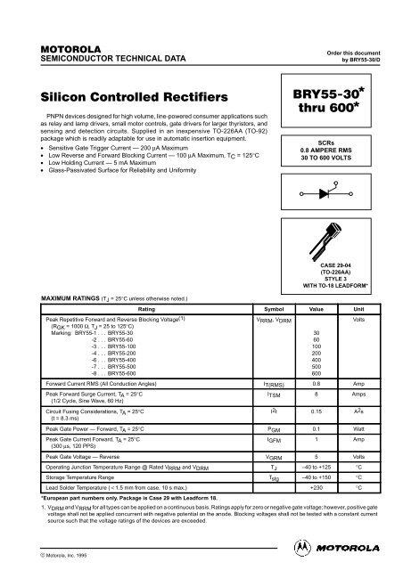
SEMICONDUCTOR TECHNICAL DATA<br />
Order this document<br />
by <strong>BRY55</strong>-<strong>30</strong>/D<br />
<br />
PNPN devices designed for high volume, line-powered consumer applications such<br />
as relay and lamp drivers, small motor controls, gate drivers for larger thyristors, and<br />
sensing and detection circuits. Supplied in an inexpensive TO-226AA (TO-92)<br />
package which is readily adaptable for use in automatic insertion equipment.<br />
• Sensitive Gate Trigger Current — 200 µA Maximum<br />
• Low Reverse and Forward Blocking Current — 100 µA Maximum, TC = 125°C<br />
• Low Holding Current — 5 mA Maximum<br />
• Glass-Passivated Surface for Reliability and Uniformity<br />
<br />
<br />
SCRs<br />
0.8 AMPERE RMS<br />
<strong>30</strong> TO <strong>600</strong> VOLTS<br />
CASE 29-04<br />
(TO-226AA)<br />
STYLE 3<br />
WITH TO-18 LEADFORM*<br />
MAXIMUM RATINGS (TJ = 25°C unless otherwise noted.)<br />
Peak Repetitive Forward and Reverse Blocking Voltage(1)<br />
(RGK = 1000 Ω, TJ = 25 to 125°C)<br />
Marking: <strong>BRY55</strong>-1 . . . <strong>BRY55</strong>-<strong>30</strong><br />
-2 . . . <strong>BRY55</strong>-60<br />
-3 . . . <strong>BRY55</strong>-100<br />
-4 . . . <strong>BRY55</strong>-200<br />
-6 . . . <strong>BRY55</strong>-400<br />
-7 . . . <strong>BRY55</strong>-500<br />
-8 . . . <strong>BRY55</strong>-<strong>600</strong><br />
Rating Symbol Value Unit<br />
VRRM, VDRM<br />
Forward Current RMS (All Conduction Angles) IT(RMS) 0.8 Amp<br />
Peak Forward Surge Current, TA = 25°C<br />
(1/2 Cycle, Sine Wave, 60 Hz)<br />
<strong>30</strong><br />
60<br />
100<br />
200<br />
400<br />
500<br />
<strong>600</strong><br />
Volts<br />
ITSM 8 Amps<br />
Circuit Fusing Considerations, TA = 25°C<br />
(t = 8.3 ms)<br />
I2t 0.15 A2s<br />
Peak Gate Power — Forward, TA = 25°C PGM 0.1 Watt<br />
Peak Gate Current Forward, TA = 25°C<br />
(<strong>30</strong>0 µs, 120 PPS)<br />
IGFM 1 Amp<br />
Peak Gate Voltage — Reverse VGRM 5 Volts<br />
Operating Junction Temperature Range @ Rated VRRM and VDRM TJ –40 to +125 °C<br />
Storage Temperature Range Tstg –40 to +150 °C<br />
Lead Solder Temperature (1.5 mm from case, 10 s max.) +2<strong>30</strong> °C<br />
*European part numbers only. Package is Case 29 with Leadform 18.<br />
1. VDRM and VRRM for all types can be applied on a continuous basis. Ratings apply for zero or negative gate voltage; however, positive gate<br />
voltage shall not be applied concurrent with negative potential on the anode. Blocking voltages shall not be tested with a constant current<br />
source such that the voltage ratings of the devices are exceeded.<br />
Motorola Thyristor Device Data<br />
1<br />
© Motorola, Inc. 1995
! " #$%#<br />
& '( ) ) <br />
'* <br />
# <br />
+ #<br />
<br />
<br />
!, # # <br />
& (! " <br />
## -# &<br />
<br />
#* <br />
# #<br />
# <br />
" # ./01 # # <br />
.201 .3,41 <br />
<br />
<br />
<br />
<br />
5 # # -# <br />
* # <br />
<br />
<br />
!6 "#*3* <br />
##& (!6 " # "<br />
-# -#,# # #<br />
# &<br />
<br />
7 #<br />
<br />
) ) / <br />
*8**98<br />
7 +*8**8:;<br />
3