+' +HDY\'XW\N: )UHTXHQF\FRQYHUWHU 4XLFNUHIHUHQFH

You also want an ePaper? Increase the reach of your titles
YUMPU automatically turns print PDFs into web optimized ePapers that Google loves.
<strong>+'</strong><br />
<br />
<strong>+HDY\'XW\N</strong>:<br />
<br />
)<strong>UHTXHQF\FRQYHUWHU</strong><br />
<br />
<strong>4XLFNUHIHUHQFH</strong><br />
216mm<br />
<br />
CAN<br />
RS232<br />
HD 7500<br />
H1<br />
H2<br />
H3<br />
CLOSE<br />
COM<br />
OPEN<br />
GND<br />
Out1<br />
Out2<br />
Out3<br />
+24V<br />
In1<br />
In2<br />
306mm<br />
In3<br />
In4<br />
GND<br />
AGND<br />
+24V<br />
PWM Out<br />
PWM In<br />
Ana Out<br />
Ana In<br />
10V Ref<br />
U<br />
V<br />
W<br />
PE<br />
PE<br />
L+<br />
RB<br />
L-<br />
PE<br />
L1<br />
L2<br />
L3<br />
&$87,21<br />
Risk of Electric Shock.<br />
The electrical connection<br />
remain life for at least 5<br />
min. after main separation.<br />
PTC<br />
<br />
<br />
<br />
<br />
Version: 13.09.2005 - 1 -
7DEOHRIFRQWHQWV<br />
29(59,(: <br />
,QWURGXFWLRQ <br />
1.1.1 General 4<br />
1.1.2 Block diagram 4<br />
&KDUDFWHULVWLFV <br />
1.2.1 Major characteristics 5<br />
1.2.2 Capability characteristic 5<br />
1.2.3 Protection features 5<br />
7HFKQLFDOVSHFLILFDWLRQ <br />
,167$//$7,21 <br />
,QWURGXFWLRQ <br />
,QVWDOODWLRQRSWLRQV <br />
2.2.1 Installation thermal separated 7<br />
2.2.2 Installation with “Cold Plate“ 7<br />
(OHFWULFDOLQVWDOODWLRQ <br />
7HUPLQDODVVLJQPHQW <br />
2.4.1 Terminal description 8<br />
2.4.2 Pin description of X1 9<br />
2.4.3 Pin description of X2 9<br />
2.4.4 Pin description of X3 9<br />
2.4.5 Pin description of H1 – H4 10<br />
2.4.6 Pin description of T1 – T4 10<br />
2.4.7 Pin description of CAN 10<br />
2.4.8 Pin description of RS232 10<br />
(0&FRPSDWLEOHLQVWDOODWLRQ <br />
,1,7,$/67$5783 <br />
6HULDOLQWHUIDFHSURWRFRO <br />
3.1.1 Control operation 12<br />
3.1.2 Programming parameters 13<br />
3.1.3 Coding of variables 15<br />
<strong>+'</strong>7RRO6RIWZDUH <br />
3.2.1 Description 17<br />
3.2.2 Installation 17<br />
3.2.3 Start the program 17<br />
3.2.4 After start 18<br />
3.2.5 Communication with frequency converter 18<br />
3.2.6 Basic functions 19<br />
3.2.7 Input of new parameters 19<br />
3.2.8 Error messages 19<br />
Version: 13.09.2005 - 2 -
6
2YHUYLHZ<br />
,QWURGXFWLRQ<br />
This short reference describes the most important characteristics of the frequency<br />
converter HD7500 and should be read carefully before the first starting. It serves the<br />
learned user to the fast assembly and starting of the converter. In additionally, the<br />
function, the connections, the installation and the parameter settings are described.<br />
*HQHUDO<br />
The major task is the electronic speed setting of an asynchronous motor.<br />
%ORFNGLDJUDP<br />
Version: 13.09.2005 - 4 -
&KDUDFWHULVWLFV<br />
0DMRUFKDUDFWHULVWLFV<br />
• Rugged design<br />
• Vibration safe<br />
• Simple installation and startup<br />
• Parameter setting using a PC<br />
• Isolated control input:<br />
o serial interface (12V level, RS232, RS485, CAN, IrDA)<br />
o 4 digital outputs<br />
o 4 digital inputs<br />
o 1 PWM input up to 1,6kHz<br />
o 1 PWM output up to 1,6kHz<br />
o 1 Analog output 0-10V/8bit<br />
o 1 Analog input 0-10V/10 bit<br />
o Relay output<br />
• U/f- characteristic, acceleration and deceleration ramps<br />
• integrated brake chopper<br />
• Wide input voltage range: 340 - 520VAC / 47 - 63Hz<br />
&DSDELOLW\FKDUDFWHULVWLF<br />
• Overload 150% for 30 seconds<br />
3URWHFWLRQIHDWXUHV<br />
• Motor protection<br />
• Over current protection<br />
• Over temperature protection<br />
• Short-circuit-protection phase against phase and/or phase against earth<br />
• Over and under voltage monitoring<br />
• I²t - monitoring<br />
• Motor over temperature protection<br />
• phase loss detection<br />
• Status indication on 3 LEDs<br />
Version: 13.09.2005 - 5 -
7HFKQLFDOVSHFLILFDWLRQ<br />
Type<br />
Input voltage<br />
Rated input frequency<br />
Motor rating<br />
Output voltage<br />
Rated output current<br />
Output frequency<br />
Switching frequency<br />
Continuous brake<br />
power<br />
Pulse brake power<br />
HD7500<br />
400V -15% + 30%, 3ph<br />
47 – 63Hz<br />
7,5kW<br />
3 x 0..400V<br />
17A<br />
1 – 100Hz<br />
8kHz<br />
200W<br />
2kW für/for 1sec<br />
Storage temperature -40°C – 85°C<br />
Ambient humidity<br />
95% (non-condensing)<br />
Ambient temperature -20 – 50°C<br />
Maximum Altitude<br />
bis 2000m / up to 2000m<br />
Type<br />
Height<br />
Width<br />
Length<br />
Weight<br />
HD7500<br />
306mm<br />
216mm<br />
164mm<br />
~9kg<br />
Version: 13.09.2005 - 6 -
,QVWDOODWLRQ<br />
,QWURGXFWLRQ<br />
All installation operations shell be carried out after disconnection of the electrical<br />
supply. Risk of electrical shock. The frequency converter and the electrical<br />
connections remain life for up to 5min. after mains separation.<br />
Ensure correct earthing connection of the frequency converter. An inappropriate earth<br />
connection can destroy the frequency converter and causes risk of electrical shock for<br />
persons.<br />
<br />
,QVWDOODWLRQRSWLRQV<br />
,QVWDOODWLRQWKHUPDOVHSDUDWHG<br />
For thermal separated installation the standard heat sink is mounted in the<br />
installation wall.<br />
,QVWDOODWLRQZLWK³&ROG3ODWH³<br />
The HD 7500 frequency converters is available with „Cold Plate“ and can be mounted<br />
directly to an external heat sink or on an enclosure. The area of contact should be as<br />
big as the cold plate of the frequency converter.<br />
Version: 13.09.2005 - 7 -
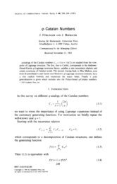
(OHFWULFDOLQVWDOODWLRQ<br />
7HUPLQDODVVLJQPHQW<br />
216mm<br />
CAN<br />
RS232<br />
HD 7500<br />
H1<br />
H2<br />
H3<br />
CLOSE<br />
COM<br />
OPEN<br />
GND<br />
Out1<br />
Out2<br />
Out3<br />
+24V<br />
In1<br />
In2<br />
;<br />
306mm<br />
;<br />
In3<br />
In4<br />
GND<br />
AGND<br />
+24V<br />
PWM Out<br />
PWM In<br />
Ana Out<br />
Ana In<br />
10V Ref<br />
U<br />
V<br />
W<br />
PE<br />
PE<br />
L+<br />
RB<br />
L-<br />
PE<br />
L1<br />
L2<br />
L3<br />
Risk of Electric Shock.<br />
The electrical connection<br />
remain life for at least 5<br />
min. after main separation.<br />
PTC<br />
+<br />
<br />
7<br />
<br />
7<br />
<br />
&$87,21<br />
7<br />
7 <br />
;<br />
7HUPLQDOGHVFULSWLRQ<br />
¢¡¤£¦¥ §¤¥©¨¤ <br />
X1<br />
X2<br />
X3<br />
H1 – H4<br />
T1 – T4<br />
CAN<br />
RS232<br />
power supply, motor and brake resistor terminal of the frequency converter<br />
control terminal of the frequency converter<br />
terminal for motor protection<br />
status indication<br />
control panel<br />
terminal for CAN connection<br />
terminal for serial interface<br />
Version: 13.09.2005 - 8 -
3LQGHVFULSWLRQRI;<br />
¢¡¤£¦¥ ¥©¤¥ §¤¥©¨¤ <br />
U, V, W - motor terminal, voltage output of the frequency converter<br />
PE - earth terminal of the frequency converter<br />
L+ - positive DC bus link<br />
RB - connection for brake resistor<br />
L- - negative DC bus link<br />
L1 - L3<br />
3 ~ AC,<br />
340..520V<br />
3LQGHVFULSWLRQRI;<br />
power supply terminal of the frequency converter<br />
CLOSE<br />
COM<br />
OPEN<br />
125 Vac / 0.3 A<br />
60 Vdc / 0.5A<br />
30 Vdc / 1 A<br />
relay closer<br />
relay common<br />
relay output opener<br />
¢¡¤£¦¥ ¥©¤¥ ¥¨ © <br />
GND 0V reference potential for digital outputs<br />
Out1<br />
Out2<br />
Out3<br />
Output Voltage:<br />
+5V, +15V or<br />
+24V<br />
max. 10mA<br />
digital I/O 1, internal pull up (10k<br />
digital I/O 2, internal pull up (10k<br />
digital I/O 3, internal pull up (10k<br />
+24V +20 .. 26V power supply for digital inputs<br />
In1<br />
digital input 1, internal pull up (10k<br />
In2<br />
In3<br />
HIGH(+10 ...<br />
+32V)<br />
LOW(0 ... +2V)<br />
digital input 2, internal pull up (10k<br />
digital input 3, internal pull up (10k<br />
In4<br />
digital input 4, internal pull up (10k<br />
GND 0V reference potential for digital inputs<br />
AGND 0V reference potential for analog inputs<br />
+24V +20 .. 26V power supply for digital inputs<br />
PWM out 0 .. +10V PWM output up to 1,6kHz<br />
PWM in 0 .. +10V PWM input up to 1,6kHz<br />
Ana out 0 .. +10V analog output<br />
Ana in 0 .. +10V analog input<br />
+10V Ref +10V Reference for analog Input<br />
3LQGHVFULSWLRQRI;<br />
PTC Resistive input for motor thermal protection device (PTC, Klixon)<br />
<br />
Version: 13.09.2005 - 9 -
3LQGHVFULSWLRQRI+±+<br />
H1 red warning or error<br />
H2 amber operation<br />
H3 green power on<br />
H4 - 7-segment Display<br />
3LQGHVFULSWLRQRI7±7<br />
T1 Ok select or Ok<br />
T2 ESC escape or delete<br />
T3 Up up or increment<br />
T4 Down down or decrement<br />
3LQGHVFULSWLRQRI&$1<br />
Pin1 +5V +5V power supply<br />
Pin2 CANL CAN low line<br />
Pin3 CANG Shield for CAN connection<br />
Pin4 NC Not connected<br />
Pin5 NC Not connected<br />
Pin6 GND Ground for CAN connection<br />
Pin7 CANH CAN high line<br />
Pin8 NC Not connected<br />
Pin9 +5V +5V power supply<br />
3LQGHVFULSWLRQRI56<br />
Pin1 +15V +15V power supply<br />
Pin2 TxD Transmit, 9600 baud, 8,N,1, start bit 10V<br />
Pin3 RxD Receive, 9600 baud, 8,N,1, start bit 10V<br />
Pin4 DTR power control for in circuit programming ICT Programming<br />
Pin5 GND reference potential<br />
Pin6 24V +24V power supply, Hardware selectable<br />
Pin7 NC Not connected<br />
Pin8 A Output A for RS485, optional 12V TTL serial output (Hardware selectable)<br />
Pin9 B Output B for RS485, optional 12V TTL serial input (Hardware selectable)<br />
Version: 13.09.2005 - 10 -
(0&FRPSDWLEOHLQVWDOODWLRQ<br />
Connect the frequency converter to the mounting plate with lock washer. If the<br />
mounting plate is varnished, remove the varnish in mounting area.<br />
Lay motor, power line and signal cables as far away from each other as possible and<br />
separately. Crossing of power cables and control cable should be at an angle of 90<br />
degree.<br />
It is recommended that the motor cable is screened. Connect the shielding on both<br />
sides.<br />
Lay the cable as close as possible to the reference potential.<br />
Version: 13.09.2005 - 11 -
,QLWLDOVWDUWXS<br />
6HULDOLQWHUIDFHSURWRFRO<br />
&RQWURORSHUDWLRQ<br />
+RVW)8<br />
¡ ©!© ¥ ¨¢<br />
" ¢§<br />
¥¤$%©¥ &¤' #<br />
¥¤$%©¥ &( #<br />
)¢¥¢*+¨%¤£<br />
10110100b B4h<br />
1xxxxxxxb<br />
xxxxxxx according to variable coding HD7500<br />
for normal operation coding is 10000000b<br />
FFFFFFFFb FFFFFFF, target frequency of the motor in 1 Hz steps<br />
FFFF000Rb<br />
FFFFFFF, target frequency of the motor in 1/16 Hz steps<br />
R direction of rotation (0..left, 1..right)<br />
xxxxxxxxb start byte + (coding rotate left 1) + (frequency1 rotate left 2) + (frequency2 rotate left 2)<br />
)8+RVW<br />
¨¢ ¡ ©!© ¥<br />
¢§ "<br />
¡, ©¨©-.¥,'<br />
01001011b<br />
0xxxxxxxb<br />
AAAAAAAAb<br />
4Bh<br />
xxxxxx according to variable coding HD7500<br />
for normal operation coding is 00000000b<br />
the requested coding will be answered<br />
¡ ©¨¢-.¥ ¢2 ¥¤$%¢¥©¨¢ ¥¤§3©§ "¦4 ¨¤¥¢¥657 '©7 5¤8<br />
////////10<br />
for normal operation with coding 00000000b, the answer is the Failflag register.<br />
00000000b -> no error<br />
¡, ©¨©-.¥, (<br />
////////10 ¡ ©¨¢-.¥ ¢2 ¥¤$%¢¥©¨¢ ¥¤§3©§ "¦4 ¨¤¥¢¥657 '©7 5¤8<br />
AAAAAAAAb for normal operation with coding 00000000b, the answer is the Failflag register.<br />
00000000b -> no error<br />
xxxxxxxxb start byte + (coding rotate left 1) + (answer1 rotate left 2) + (answer2 rotate left 2)<br />
)¢¥¢*+¨%¤£<br />
Version: 13.09.2005 - 12 -
3URJUDPPLQJSDUDPHWHUV<br />
'DWD+RVW)8<br />
¨¢ ¡ ©!© ¥<br />
¡¤§§ ¥¨¢¨<br />
11010xxxb<br />
xxxxxxxxb<br />
xxxxxxxxb<br />
11011010b<br />
D3h – WRITE<br />
D4h – READ<br />
D5h – ERASE<br />
WRITE xxxxxx according to parameter address<br />
READ xxxxxx according to parameter address<br />
address for ERASE E²PROM<br />
¡© ¡,'<br />
xxxxxxxxb<br />
00000000b<br />
01011011b<br />
WRITE – data for address high<br />
READ<br />
ERASE<br />
¡© ¡¢(<br />
xxxxxxxxb<br />
00000000b<br />
01011011b<br />
WRITE – data for address low<br />
READ<br />
ERASE<br />
xxxxxxxxb start byte + (address rotate left 1) + (data1 rotate left 2) + (data2 rotate left 2)<br />
)¢¥¢*+¨%¤£<br />
'DWD)8±+RVW<br />
00101100b<br />
xxxxxxxxb<br />
2Ch<br />
WRITE xxxxxx according to parameter address<br />
¨¢ ¡ ©!© ¥<br />
xxxxxxxxb<br />
11011010b<br />
READ xxxxxx according to parameter address<br />
address for ERASE E²PROM<br />
¡¤§§ ¥¨¢¨<br />
xxxxxxxxb<br />
xxxxxxxxb<br />
WRITE – data for address high<br />
READ – data for address high<br />
¡© ¡,'<br />
00000000 ERASE<br />
xxxxxxxxb<br />
WRITE – data for address low<br />
¡© ¡¢(<br />
xxxxxxxxb<br />
0000000x<br />
READ – data for address low<br />
ERASE<br />
0 erasing ok<br />
1 error at erasing<br />
xxxxxxxxb start byte + (address rotate left 1) + (data1 rotate left 2) + (data2 rotate left 2)<br />
)¢¥¢*+¨%¤£<br />
<br />
Version: 13.09.2005 - 13 -
Version: 13.09.2005 - 14 -
&RGLQJRIYDULDEOHV<br />
¤" ¡, §¥¨ © <br />
¢,§ ¤¡, ¥<br />
b15 stop motor<br />
b14 not used<br />
b13 rectifier temperatur alarm<br />
b12 power module temperature alarm<br />
b11 motor temperatur alarm<br />
b10 Brake overload<br />
b9 I²t error<br />
0 Failflag<br />
b8 over current<br />
b7 DC Line error<br />
b6 Phase error<br />
b5 input voltage high<br />
b4 input voltage low<br />
b3 fault high side<br />
1 SystemStartUp<br />
2 SystemWarning<br />
3<br />
Reset Status<br />
Register<br />
b2 fault phase W<br />
b1 fault phase V<br />
b0 fault phase U<br />
b15 not used<br />
b14 not used<br />
b13 not used<br />
b12 not used<br />
b11 not used<br />
b10 not used<br />
b9 Ventilation On<br />
b8 Brake On<br />
b7 StartUpOk<br />
b6 RectifierOn<br />
b5 UzkLoadOk<br />
b4 UzkHOk<br />
b3 UzkOk<br />
b2 ElkoLoad<br />
b1 PhaseOk<br />
b0 HardwareOk<br />
b15 not used<br />
b14 not used<br />
b13 not used<br />
b12 SerialTimeout<br />
b11 I²tCount<br />
b10 CurrentReferencWarning<br />
b9 Current overrated<br />
b8 GLTempWarning<br />
b7 IPMTEmpWarning<br />
b6 MotorTempWarning<br />
b5 UzkHOutofRange<br />
b4 UzkOutofRange<br />
b3 L3Fail<br />
b2 L2Fail<br />
b1 L1Fail<br />
b0 Varistor Fail<br />
.7 power On reset (POR)<br />
.6 external reset (Pin)<br />
.5 watchdog (COP)<br />
.4 illegal opcode (ILOP)<br />
.3 illegal address reset (ILAD)<br />
.1 low voltage inhibit reset (LVI)<br />
4 Version Software Version xx.xx<br />
5 Bulid Bulid<br />
Version: 13.09.2005 - 15 -
6 GLTemp Rectifier Temperature measurement point in °C<br />
7 IPMTemp IPM Temperature measurement point in °C<br />
8 MTemp Resistance of motor temperature sensor<br />
9 Uzk main DC voltage 1bit ~ 4V<br />
10 UzkH half main DC voltage 1bit ~ 4V<br />
11 Izk main DC current 1bit ~ 20mA<br />
12 IzkR Reference 128bit<br />
13 IzkM Main DC Current with reference 128bit<br />
14 AnaIn Analog input value in bit<br />
15 - Not used<br />
16 I²t high<br />
17 I²t low byte<br />
maximum load integral<br />
18 BrakeI²t high<br />
19 BrakeI²t low Brake load integral<br />
20 Brake PWM<br />
21 SerialTarget target output frequency serial<br />
22 CANTarget target output frequency CAN<br />
23 DigitalTarget target output frequency digital<br />
24 PWMTarget target output frequency PWM<br />
25 AnalogTarget target output frequency analog<br />
26 TastTarget target output frequency switches<br />
27 SerTimeOutCounter serial timeout counter<br />
28 CANTimeOutCounter CAN timeout counter<br />
29 PWMPeriode period of PWM signal<br />
30 PWMPuls width of PWM signal high<br />
31 PWMBuffer buffer for PWM signal<br />
32 coding serial interface coding<br />
33 Notstop emergency stop active<br />
34 target frequency target output frequency<br />
35 actual frequency actual output frequency<br />
36 Direction direction of rotation<br />
37 motor voltage output voltage to motor<br />
38 SinStep step width in sin table<br />
39 Pout output power<br />
40 BootTime bootstrap timer<br />
41 GenTime time of dynamic operation<br />
42 StopTime timer for emergency stop or brake<br />
43 L1FailTime time of operation without L1<br />
44 L2FailTime time of operation without L1<br />
45 L3FailTime time of operation without L1<br />
46 VFailTime time of operation without varistor<br />
47 MainFlag main loop timer<br />
48 Flag flag variable<br />
49 CycleTime cycle timer<br />
50 CountTime counter<br />
51 MTempADC ADC value of motor resistor<br />
52 GLTempADC ADC value of temp sensor<br />
53 IPMTempADC ADC value of temp sensor<br />
54 IOMode<br />
bit 15 – 12 Digital Inputs, bit 11 – 8 button inputs,<br />
low byte port output<br />
55 Uzkload main DC voltage at turn on<br />
56 BrakeGLI overload line brake<br />
Version: 13.09.2005 - 16 -
<strong>+'</strong>7RRO6RIWZDUH<br />
'HVFULSWLRQ<br />
The PC software “HD7500Tool” supports the parameter setting. This graphic user<br />
interface offers fast and simple access to the FU-parameters. With the software the<br />
parameter lists can be stored or loaded from disk.<br />
,QVWDOODWLRQ<br />
Insert the “HD7500Tool CD” into CD-Rom drive. The Setup program starts<br />
automatically. If this should not be the case, start the setup file in the root directory of<br />
the CD and follow the instructions at the screen. During the installation, a directory C:\<br />
HD7500Tool with parameter lists is created.<br />
6WDUWWKHSURJUDP<br />
Start “HD7500Tool” in your start menu.<br />
Version: 13.09.2005 - 17 -
$IWHUVWDUW<br />
&RPPXQLFDWLRQZLWKI<strong>UHTXHQF\FRQYHUWHU</strong><br />
For correct communication between frequency converter and PC the frequency<br />
converter must be connected to mains voltage. The serial connection between PC and<br />
frequency converter must be made either by the options print or a peripheral interface<br />
adapter. Select the COM port on the user interface.<br />
Version: 13.09.2005 - 18 -
%DVLFIXQFWLRQV<br />
New<br />
Open File<br />
Save File<br />
Print<br />
DOWNLOAD<br />
UPLOAD<br />
Clear FU<br />
The existing parameter list is replaced by empty default table.<br />
Opens a saved parameter list.<br />
ATTENTION: parameter lists are “.csv” files.<br />
Saves the parameter list.<br />
ATTENTION: parameter lists are “.csv” files.<br />
Prints the parameter list.<br />
Downloads the parameter list of the connected frequency converter.<br />
ATTENTION: Works only if frequency converter is cleared.<br />
Uploads the parameter list to the connected frequency converter.<br />
Clears the parameter in connected frequency converter.<br />
EXIT<br />
Terminates the program.<br />
&20±LQWHUIDFHEXWWRQ<br />
Define the serial communication port to be used.<br />
,QSXWRIQHZSDUDPHWHUV<br />
The area DESCRITPION, COSTUMER and PROJEKT are for additional definitions of<br />
the parameter list. The additional information is stored in the “.csv” file. To the<br />
frequency converter only changes in column value become operative. This column<br />
value is updated at download and is sent to the frequency converter at upload.<br />
(UURUPHVVDJHV<br />
9DOXHRXWRIUDQJH<br />
<br />
During download this area shows the index of the value which is out of range. If a<br />
value is out of range during uploading the parameter is replaced with a standard<br />
value.<br />
Recommended system requirements:<br />
Pentium III, Celeron 600 MHz or equivalent, 256MB RAM, 1024x768 pixel resolutions,<br />
16 Bit color depth, 30MB free disk space<br />
Microsoft Windows 98/ME/2000/NT 4.0 with SP 6/XP<br />
Version: 13.09.2005 - 19 -
6\VWHPSDUDPHWHUV<br />
3DUDPHWHUWDEOHDQGGHVFULSWLRQ<br />
¤§¤¥©9 ¢¡ ¡£:¥© ¥; ©¡£:¥ ¡,,,7 %, ¡, ¢"¥ ¡¤"¤¥<br />
0.0 line input voltage minimum Uinmin [V] 400 - 560 480 0,257<br />
0.1 line input voltage maximum Uinmax [V] 560 – 750 735 0,257<br />
0.2 line input voltage hysteresis Uinhys [V] 0-10 2 0,257<br />
for control of line input voltage the sine peak voltage is used<br />
for DC input use the corresponding values.<br />
0.3 Rated DC link voltage Uzksoll [V] 400 – 750 560 0,257<br />
Rated value of DC link voltage reference for motor control<br />
(This value is only a reference for motor control and should be 560V)<br />
0.4 DC link voltage minimum Uzkmin [V] 400 – 560 480 0,257<br />
0.5 DC link voltage maximum Uzkmax [V] 560 – 750 735 0,257<br />
0.6 DC link voltage hysteresis Uzkhyst [V] 0-10 4 0,257<br />
¢= ¤©¡, ¡£¦¥ ¥,2 =%©,%©%, ¥, ©<br />
1.0 Rated current Inenn [A] 0-50 17 0,64<br />
1.1 Over current Iover [A] 0-50 25 0,64<br />
1.2 Reduction factor Ired [%] 101-130 105 1<br />
1.3 Maximum load integral GLI [A²s] 0 0<br />
(Iover*0,64)² -<br />
(Inenn*0,64)²<br />
Set rated motor current (Inenn) and over current (Iover) should be maximum 150% of rated current.<br />
From rated current and over current the maximum load integral is calculated.<br />
The reduction factor gives the recovery time when overshooting the rated current. As shown in the diagram, with a<br />
reduction factor of 1,05 the frequency converter recovers in approximately 700 seconds from an overshooting<br />
during 30 seconds with Over current.<br />
Version: 13.09.2005 - 20 -
¢ ©¤¢¡ ¡£:¥© ¥2 %©? 2)¢¡ ¡¢@ ¥, ¨¢ <br />
2.0 U/f – characteristic IxR (eff) IxR [V] 0-50 20 0,64<br />
2.1 U/f – characteristic fx fx [Hz] 0-100 25 1<br />
2.2 U/f – characteristic Ux (eff) Ux [V] 0-400 200 0,64<br />
2.3 U/f – characteristic feck feck [Hz] 0-100 50 0,64<br />
2.4 U/f – characteristic Ueck(eff) Ueck [V] 0-400 400 0,64<br />
2.5 U/f – characteristic fmax fmax [Hz] 0-100 50 1<br />
2.6 U/f – characteristic Umax (eff) Umax [V] 0-400 400 0,64<br />
2.7 U/f – characteristic ramp + Ramp1+ [Hz/s] 1-100 5 1,28<br />
2.8 U/f – characteristic ramp - Ramp- [Hz/s] 1-100 5 1,28<br />
2.9 U/f – characteristic ramp + Ramp2+ [Hz/s] 1-100 5 1,28<br />
2.10 U/f – characteristic fxramp fxramp [Hz] 1-100 5 1<br />
2.11 U/f – characteristic fmin fmin [Hz] 1-100 0 1<br />
Ramp1 + for frequencies between 0 Hz and fxramp, Ramp2+ for frequencies between fxramp and fmax.<br />
fmin is the minimal frequency at startup.<br />
¢ © ¢¢¡, ¡£:¥© ¥,2 ¡*@¥<br />
3.0 DC link voltage, brake on Uzkbon [V] 700 – 800 750 0,257<br />
3.1 DC link voltage, brake off Uzkboff [V] 700 – 800 740 0,257<br />
3.2 Brake resistor value Rbrake [Ohm] 60 – 500 150 1<br />
3.3 Brake resistor nominal power Pbrake [W] 50 – 1000 300 1<br />
3.4 Brake resistor peak power Ppeakbrake [W] 100 – 5000 1000 1<br />
3.5 Time to mean nominal Pb Tbrakenom [s] 10 – 240 10 1<br />
Version: 13.09.2005 - 21 -
©= ©¤©¡, ¡¤£¦¥© ¥,2 2 ¥ §:-.¥©¡,*+¥, "A ¡ ¤"¥<br />
4.0 Pout max in field weakening range Poutmax [W] 100-2000 500 1<br />
4.1<br />
P-part of controller in field weakening<br />
[10 -<br />
Kp<br />
range<br />
Hz/W]<br />
0-50 7,9 2,52<br />
4.2<br />
I-part of controller in field weakening<br />
[10 -<br />
Ki<br />
range<br />
Hz/Ws]<br />
0-1000 396,5 0,013<br />
At operation in field weakening range (feck to fmax) the output power is regulated to Poutmax.<br />
¢ © ¢¢¡, ¡£:¥© ¥,2 ¥©9¢ ¥ ¤§¥¢§¦2%, ¤@ = ¨<br />
5.0 Maximum time for dynamic operation tgen [ms] 0-1000 500 0,2<br />
Maximum time for dynamic operation during deceleration.<br />
5.1 Duration of stop brake tstop [ms] 0-5000 2500 0,2<br />
A stop brake with IxR for tstop after deceleration. To deactivate set to 0.<br />
5.2 On-time emergency stop brake Tnotstop [s] 0-10 5 200<br />
5.3 DC brake power for emergency stop Pnotstop [W] 0-500 260 25<br />
¢ © ¤¢¡, ¡£:¥© ¥¤2 ¤ ¥¢ B2 ¥¢¡©% ¥¨<br />
6.0<br />
Motor temperature monitoring<br />
(0..MotorPTC, 1..switch contact)<br />
Mschutz [sel] 0-1 0 1<br />
6.1 Minimum PTC resistance Rptcmin [Ohm] 0-500 0 1<br />
6.2 Maximum PTC resistance Rptcmax [Ohm] 10-10000 747 1<br />
6.3 Warning PTC resistance Rptcwarn [Ohm] 10-10000 500 1<br />
6.4 Hysterics PTC resistance PTChys [%] 0-20 2 2,56<br />
Parameter for monitoring of motor PTC. With Mschutz a motor PTC monitoring or switching contact can be selected<br />
6.5 Minimum electronic temperature Etmin [°C] -20-20 0 1<br />
6.6 Maximum electronic temperature Etmax [°C] 30-100 78 1<br />
6.7 Warning electronic temperature Ewarn [°C] 30-100 70 1<br />
6.8 Hysterics electronic temperature Ethys [%] 0-20 0,8% 2,56<br />
Parameter for monitoring of electronic temperature.<br />
Version: 13.09.2005 - 22 -
¢ © ¢¢¡, ¡£:¥© ¥,2 ¥¤$%¢¥, ¢©!6¨¤¥ ¢"<br />
9.0 Target frequency Sollvor [sel] 0-3 0 1<br />
0.. target frequency using serial communication<br />
1.. target frequency using CAN<br />
2.. target frequency using digital I/Os<br />
3.. target frequency using PWM I/Os<br />
4.. target frequency using Analog I/Os<br />
5.. target frequency using tastatur<br />
¢= ¤©¡, ¡£¦¥ ¥,2 ¨¢¥ ¡©¢,£3£A%, , ©¡© =<br />
10.0 communication timeout Timeout [ms] 10 – 10000 100 0,2<br />
10.1 enable IrDA communication IrDA [sel] 0-1 0 1<br />
After communication Timeout the motor is turned off.<br />
If IrDA is set to 1, the IR communication port is enabled.<br />
¢= ¤©¡, ¡£¦¥ ¥,2 =C /ED ¢,£3£A%, ©¡© =<br />
11.0 CANMode CANMode [sel] 0-1 0 1<br />
11.1 CANSpeed CANSpeed [sel] 0-3 0 1<br />
11.2 CANAddress CANAdd [sel] 0-63 0 1<br />
CANMode<br />
0.. inactive<br />
1.. active<br />
CANSpeed<br />
0.. 125kbit/s<br />
1.. 250kbit/s<br />
2.. 500kbit/s<br />
3.. 1Mbit/s<br />
CANAddress (Node_ID)<br />
Version: 13.09.2005 - 23 -
¢= ¤©¡, ¡£:¥© ¥,2 ;; " ¡,©F ? G¨<br />
12.0 digital mode Digmode [sel] 0-3 0 1<br />
12.1 fix frequency f0 f0 [Hz] 0-100 0 256<br />
12.2 fix frequency f1 f1 [Hz] 0-100 0 256<br />
12.3 fix frequency f2 f2 [Hz] 0-100 0 256<br />
12.4 fix frequency f3 f3 [Hz] 0-100 0 256<br />
12.5 fix frequency f4 f4 [Hz] 0-100 0 256<br />
12.6 fix frequency f5 f5 [Hz] 0-100 0 256<br />
12.7 fix frequency f6 f6 [Hz] 0-100 0 256<br />
12.8 fix frequency f7 f7 [Hz] 0-100 0 256<br />
12.9 output voltage Uout [sel] 0-3 0 1<br />
12.10 Output mode Outmode [sel] 0-1 0 1<br />
Digital mode:<br />
0.. fix frequency with In4 = start/stop<br />
1.. fix frequency with In3 = left/right, In4 = start/stop<br />
2.. digital potentiometer with In3 = left/right, In4 = start/stop, In1 = up, In2 = down<br />
In3 In2 In1 frequency<br />
0 0 0 f0<br />
0 0 1 f1<br />
0 1 0 f2<br />
0 1 1 f3<br />
1 0 0 f4<br />
1 0 1 f5<br />
1 1 0 f6<br />
1 1 1 f7<br />
3.. Test mode Out1 = In1, Out2 = In2, Out3 = In3, Relay = In4<br />
Output voltage: 0.. 24V, 1..15V, 2..5V, 3..PullUp inactive (logic inverted)<br />
Output mode: 0.. Out1 = H1, Out2 = H2, Out3 = H3<br />
1.. Out1 = under voltage warning<br />
Out2 = H2, Out3 = H1<br />
¢ © ¢¢¡, ¡£:¥© ¥,2 H,IKJLF ? G1¨<br />
13.0 PWM mode PWMmode [sel] 0-1 0 1<br />
For duty cycles from 0 to 100% set PWMmode to 0 and for 10% to 90% to 1.<br />
©= ¤©¡, ¡¤£¦¥© ¥,2 ¡, ©¡, ,"3F ? G¨<br />
14.0 analog input mode Anainmode [sel] 0-3 0<br />
0.. input 0-5V<br />
1.. input 0 -10V<br />
2.. input 0-20mA<br />
3.. input 4-20mA<br />
14.1 analog output mode Anaoutmode [sel] 0-1 0<br />
0.. output 0-5V<br />
1.. output 0 -10V<br />
Version: 13.09.2005 - 24 -
M<br />
5<br />
¥¢¥, ¦N,O "<br />
M<br />
(<br />
¡£A¢¥,NO<br />
M<br />
'<br />
¥¤§AN,O <br />
<br />
<br />
(UURUGLDJQRVWLFVDQGIDLOXUHHOLPLQDWLRQ<br />
2SHUDWLQJVWDWXVLQGLFDWLRQ<br />
§¤¥©¨ <br />
off<br />
on<br />
off off no supply or error<br />
X on in circuit programming is active<br />
off<br />
off<br />
not ready for operation<br />
on<br />
Error (see Error table)<br />
off<br />
motor runs<br />
blink blink motor runs, Warning (see Warning table)<br />
on<br />
motor runs, Error (see Error table)<br />
off<br />
ready for operation<br />
on<br />
blink ready for operation, Warning (see Warning table)<br />
on<br />
ready for operation, Error (see Error table)<br />
<br />
(UURUWDEOH<br />
M=P<br />
§¥¨ © <br />
1 no parameter setting<br />
2 electronic temperature<br />
3 motor temperature<br />
4 brake overload<br />
5 I²t overload<br />
6 over current<br />
7 DC Line<br />
8 phase error<br />
9 input voltage to high<br />
10 input voltage to low<br />
11 high side fail<br />
12 phase W fail<br />
13 phase V fail<br />
14 phase U fail<br />
<br />
:DUQLQJWDEOH<br />
M=P<br />
§¥¨ © <br />
1 output current over rated<br />
2 electronic temperature goes high<br />
3 motor temperature goes high<br />
4 varistors are not more connected<br />
Version: 13.09.2005 - 25 -
6DIHW\DQGRSHUDWLQJLQVWUXFWLRQV<br />
To ensure safe and faultless operation of the frequency converter, appropriate<br />
transport, correct storage, assembly and installation as well as careful handling is<br />
required.<br />
In operation the frequency converter has life unisolated parts, as well as hot surfaces.<br />
In case of improper use, wrong installation or maloperation, there is the danger of<br />
serious personal injury and damage to property.<br />
All operations are to be carried out by skilled technical personnel. For proposes of<br />
these basic safety instructions, “skilled technical personnel” means persons who are<br />
familiar with the installation, mounting, commissioning and operation of the product<br />
and have the qualifications need for such installation.<br />
After disconnection of the frequency converter from the voltage supply, live appliance<br />
parts and power terminals must not be touched immediately because of possible<br />
energized capacitors. Wait at least 5min before touching the frequency converter.<br />
Version: 13.09.2005 - 26 -


![55721335-d6fe09eb5ffdcc87dbf6c3f0b5bbda07d2261e98[1]](https://img.yumpu.com/56533583/1/186x260/55721335-d6fe09eb5ffdcc87dbf6c3f0b5bbda07d2261e981.jpg?quality=85)