Scan design techniques – solutions to recommended exercises
Scan design techniques – solutions to recommended exercises
Scan design techniques – solutions to recommended exercises

You also want an ePaper? Increase the reach of your titles
YUMPU automatically turns print PDFs into web optimized ePapers that Google loves.
Introduction <strong>to</strong> DFT Techniques in Digital Circuits - ©2002 jmf@fe.up.pt<br />
<strong>Scan</strong> <strong>design</strong> <strong>techniques</strong> <strong>–</strong> <strong>solutions</strong> <strong>to</strong> <strong>recommended</strong> <strong>exercises</strong><br />
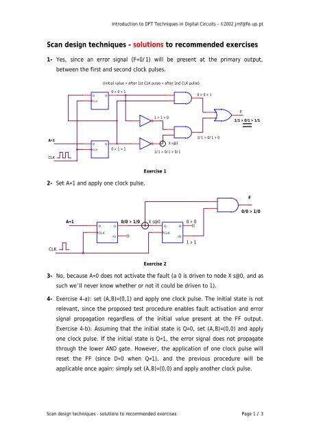
1- Yes, since an error signal (F=0/1) will be present at the primary output,<br />
between the first and second clock pulses.<br />
(initial value > after 1st CLK pulse > after 2nd CLK pulse)<br />
D<br />
Q<br />
0 > 0 > 1<br />
0 > 0 > 1<br />
CLK<br />
1 > 1 > 0<br />
F<br />
1/1 > 0/1 > 1/1<br />
A=1<br />
CLK<br />
D<br />
CLK<br />
Q<br />
0 > 1 > 1<br />
X s@1<br />
1/1 > 0/1 > 0/1<br />
1/1 > 0/1 > 0<br />
Exercise 1<br />
2- Set A=1 and apply one clock pulse.<br />
F<br />
0/0 > 1/0<br />
A=1<br />
D<br />
Q<br />
0/0 > 1/0 X s@0<br />
D<br />
Q<br />
0 > 0<br />
CLK<br />
CLK<br />
/Q<br />
CLK<br />
/Q<br />
1 > 1<br />
Exercise 2<br />
3- No, because A=0 does not activate the fault (a 0 is driven <strong>to</strong> node X s@0, and as<br />
such we’ll never know whether or not it could be driven <strong>to</strong> 1).<br />
4- Exercise 4-a): set (A,B)=(0,1) and apply one clock pulse. The initial state is not<br />
relevant, since the proposed test procedure enables fault activation and error<br />
signal propagation regardless of the initial value present at the FF output.<br />
Exercise 4-b): Assuming that the initial state is Q=0, set (A,B)=(0,0) and apply<br />
one clock pulse. If the initial state is Q=1, the error signal does not propagate<br />
through the lower AND gate. However, the application of one clock pulse will<br />
reset the FF (since D=0 when Q=1), and the previous procedure will be<br />
applicable once again: simply set (A,B)=(0,0) and apply another clock pulse.<br />
<strong>Scan</strong> <strong>design</strong> <strong>techniques</strong> <strong>–</strong> <strong>solutions</strong> <strong>to</strong> <strong>recommended</strong> <strong>exercises</strong> Page 1 / 3
Introduction <strong>to</strong> DFT Techniques in Digital Circuits - ©2002 jmf@fe.up.pt<br />
A=0<br />
B=1<br />
X<br />
0/1<br />
X s@1<br />
0/1<br />
D<br />
Q<br />
F=0/1<br />
0<br />
X<br />
0<br />
CLK<br />
CLK<br />
/Q<br />
Exercise 4-a)<br />
A=0<br />
1<br />
0<br />
B=0<br />
1/0<br />
D<br />
Q<br />
F=1/0<br />
X<br />
s@0<br />
1/0<br />
1<br />
1<br />
1/0<br />
CLK<br />
CLK<br />
/Q<br />
Exercise 4-b)<br />
5- (Entrada primária: Primary input; Saída primária: Primary output; Estado seguinte:<br />
Next state; Estado actual: Present state; Modo de teste: Test mode; Entr. série: Serial<br />
input; Saída série: Serial output) Setting (X,Y)=(0,0) and (Q1,Q0)=(X,1) will<br />
activate the fault and propagate the error signal <strong>to</strong> the output of the OR gate.<br />
As such, the following sequence may be used:<br />
- Set (Y,X)=(0,0), so that the fault is activated when we get <strong>to</strong> state<br />
(Q1,Q0)=(X,1)<br />
- Set (serial input, test mode)=(1,1) <strong>to</strong> move in<strong>to</strong> scan mode and prepare <strong>to</strong><br />
scan 1s<br />
- Apply two clock pulses (the fault will be activated when the second clock<br />
pulse is applied)<br />
- Set (serial input, test mode)=(X,0) <strong>to</strong> capture the error signal in<strong>to</strong> Q1<br />
- Apply one clock pulse (<strong>to</strong> capture the error signal present at the OR gate<br />
output)<br />
- Set (serial input, test mode)=(X,1) <strong>to</strong> move in<strong>to</strong> scan mode (so that the<br />
error signal may be shifted out)<br />
- Apply one clock pulse: this will bring the error signal in<strong>to</strong> the serial output<br />
<strong>Scan</strong> <strong>design</strong> <strong>techniques</strong> <strong>–</strong> <strong>solutions</strong> <strong>to</strong> <strong>recommended</strong> <strong>exercises</strong> Page 2 / 3
Introduction <strong>to</strong> DFT Techniques in Digital Circuits - ©2002 jmf@fe.up.pt<br />
6- Applying a 0 <strong>to</strong> primary input A is sufficient, since this is enough <strong>to</strong> activate the<br />
fault and propagate the error signal <strong>to</strong> primary output D0 (no clock pulses are<br />
required).<br />
0<br />
A<br />
X s@0<br />
0<br />
1<br />
1/0<br />
0<br />
0<br />
0<br />
D1<br />
0<br />
1/0<br />
1/0<br />
1<br />
0<br />
0<br />
1/0<br />
D0<br />
0<br />
0<br />
Q1<br />
Q<br />
D<br />
D1<br />
1<br />
/Q1<br />
Q<br />
CLK<br />
0<br />
Q0<br />
Q<br />
D<br />
D0<br />
1<br />
/Q0<br />
Q<br />
CLK<br />
CLK<br />
Exercise 6<br />
<strong>Scan</strong> <strong>design</strong> <strong>techniques</strong> <strong>–</strong> <strong>solutions</strong> <strong>to</strong> <strong>recommended</strong> <strong>exercises</strong> Page 3 / 3