Potential sputtering - IAP/TU Wien - Technische Universität Wien
Potential sputtering - IAP/TU Wien - Technische Universität Wien
Potential sputtering - IAP/TU Wien - Technische Universität Wien

Create successful ePaper yourself
Turn your PDF publications into a flip-book with our unique Google optimized e-Paper software.
10.1098/rsta.2003.1300<br />
<strong>Potential</strong> <strong>sputtering</strong><br />
By Friedrich Aumayr and Hannspeter Winter<br />
Institut für Allgemeine Physik, <strong>Technische</strong> <strong>Universität</strong> <strong>Wien</strong>,<br />
Wiedner Hauptstrasse 8–10, 1040 Vienna, Austria<br />
(aumayr@iap.tuwien.ac.at)<br />
Published online 25 November 2003<br />
The potential energy stored in multiply charged ions is liberated when the ions<br />
recombine during impact on a solid surface. For certain target species this can lead<br />
to a novel form of ion-induced <strong>sputtering</strong>, which, in analogy to the usual kinetic<br />
<strong>sputtering</strong>, has been termed ‘potential <strong>sputtering</strong>’. This <strong>sputtering</strong> process is characterized<br />
by a strong dependence of the observed <strong>sputtering</strong> yields on the charge<br />
state of the impinging ion and can take place at ion-impact energies well below the<br />
kinetic <strong>sputtering</strong> threshold.<br />
We summarize a series of recent careful experiments in which potential <strong>sputtering</strong><br />
has been investigated for hyperthermal highly charged ions’ impact on various<br />
surfaces (e.g. Au, LiF, NaCl, SiO 2 ,Al 2 O 3 and MgO), present the different models<br />
proposed to explain the potential <strong>sputtering</strong> phenomenon and also discuss possible<br />
applications of potential <strong>sputtering</strong> for nanostructure fabrication.<br />
Keywords: multi-charged-ion–surface interaction;<br />
potential <strong>sputtering</strong>; hollow atoms; nanostructuring<br />
1. Introduction<br />
The interaction of energetic ions (atoms) with surfaces leads to a variety of emission<br />
phenomena (emission of electrons, photons, atoms, ions, clusters) and results in pronounced<br />
modification of the surface and near-surface regions (change in composition<br />
and structure, defect production, removal of atoms, etc.) (see, for example, Gnaser<br />
(1999) and references therein). The technological relevance of low-energy ion–surface<br />
interactions in such diverse fields as surface analysis, implantation, sputter cleaning<br />
of surfaces, thin film deposition, etc. (Murty 2002), has provided the stimulus for<br />
ongoing investigations into the responsible basic mechanisms.<br />
In kinetic <strong>sputtering</strong>, the decelerated primary projectiles usually transfer (kinetic)<br />
energy and momentum to the target atoms, displacing them from their original<br />
position and eventually causing their emission into a vacuum (Sigmund 1993). Singly<br />
charged ions with kinetic energies typically of some keV mainly interact by means of<br />
a few direct collisions with the target atoms (nuclear stopping) (Ziegler et al. 1985).<br />
For faster ions and especially swift heavy ions (typically MeV per atomic mass unit),<br />
the electronic energy loss (electronic stopping) dominates (Schiwietz et al. 2001;<br />
One contribution of 11 to a Theme ‘Sputtering: past, present and future. W. R. Grove 150th Anniversary<br />
Issue’.<br />
Phil. Trans. R. Soc. Lond. A (2004) 362, 77–102<br />
77<br />
c○ 2003 The Royal Society
78 F. Aumayr and H. Winter<br />
1000000<br />
100000<br />
W pot<br />
(q) (eV)<br />
10000<br />
1000<br />
Ar q+<br />
100<br />
Xe q+<br />
Th q+<br />
10<br />
0 20 40 60 80 100<br />
q<br />
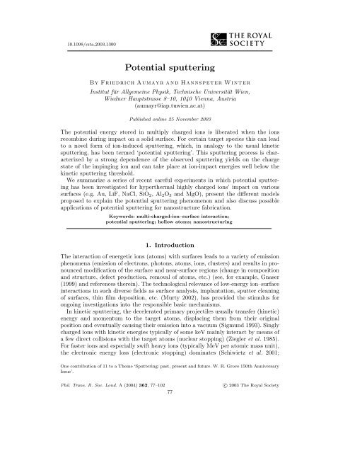
Figure 1. Total potential energy W pot(q) of multiply charged<br />
Ar q+ ,Xe q+ and Th q+ ions versus charge state q.<br />
Arnoldbik et al. 2003), leading to electronic excitation and ionization in a track a<br />
few nanometres in diameter. While the energy dissipation of the fast projectile is<br />
well understood, the conversion of electronic excitations into motion of (eventually<br />
sputtered) surface atoms is still a matter of debate.<br />
In addition to their kinetic energy, ions can also carry internal (potential) energy,<br />
particularly if the ions carry a high charge. In a highly charged ion (HCI), potential<br />
energy will be stored according to its production, when q electrons (where q is the ion<br />
charge state) have to be removed from an originally neutral atom, and this potential<br />
energy becomes rather large for high values of q, as shown in figure 1. Upon surface<br />
impact, this potential energy is available for inducing various inelastic processes,<br />
while the HCI will regain its q missing electrons to become fully neutralized again<br />
(Aumayr 1995; Arnau et al. 1997; Winter & Aumayr 1999, 2001, 2002). The HCI<br />
deposits its potential energy in a short time (typically ca. 100 fs) within a small area<br />
(typically less than 1 nm 2 ). This can lead to strong nonlinear excitation processes,<br />
exotic phenomena such as ‘hollow atom’ formation (Arnau et al. 1997; Schenkel et<br />
al. 1999; Winter & Aumayr 1999, 2002) and eventually to the removal of atoms and<br />
ions from the target surface (Aumayr et al. 1999). Since the energy for the ejection<br />
of target atoms and ions results from the potential energy of the ion, this new form of<br />
<strong>sputtering</strong> has been termed ‘potential <strong>sputtering</strong>’ (PS) (Neidhart et al. 1995b; Sporn<br />
et al. 1997; Aumayr et al. 1999).<br />
In this paper we will summarize the present knowledge on potential <strong>sputtering</strong>. To<br />
this aim we will present a short history of potential <strong>sputtering</strong> investigations in § 2<br />
and describe our experimental set-up for measuring total sputter yields and discuss<br />
critical experimental issues involved in § 3. Our experimental results are summarized<br />
in § 4, while in § 5 we present the different models proposed to explain the PS phenomenon<br />
and compare them to experimental results. Finally, in an outlook (§ 6) we<br />
discuss possible practical applications of potential <strong>sputtering</strong>.<br />
Phil. Trans. R. Soc. Lond. A (2004)
<strong>Potential</strong> <strong>sputtering</strong> 79<br />
2. History of potential <strong>sputtering</strong><br />
The first experimental work on charge-state-dependent <strong>sputtering</strong> of insulators by<br />
HCIs was carried out in Tashkent, Uzhbekistan (Radzhabov et al. 1976; Morozov et<br />
al. 1979). From this work it was concluded that, for impact of Ar q+ ions (q 5) on<br />
silicon and alkali-halide surfaces, secondary-ion yields increased rapidly both with<br />
the incident-ion charge and for decreasing impact energy. Etching patterns on a KCl<br />
surface that had previously been bombarded with equal fluxes of slow Ar q+ and<br />
Kr q+ ions were larger for higher q (Radzhabov & Rakhimov 1985). In Eccles et al.<br />
(1986) it was claimed that, for bombardment of Si with singly charged ions, sputter<br />
yields are larger by more than a factor of two than for neutral projectiles of equal<br />
mass and energy. However, for 20 keV Ar q+ (q 9) impact on an Si surface, only the<br />
secondary-ion yield increased noticeably with q, whereas the respective total sputter<br />
yields (dominated by ejection of neutral Si atoms) did not change with q (de Zwart<br />
et al. 1986). This apparent contradiction to Eccles et al. (1986) was explained by a<br />
different conductance of the Si samples.<br />
Atomic force microscopy (AFM) on mica samples irradiated with low fluences of<br />
very highly charged ions (e.g. Xe 44+ and U 70+ ) revealed single-ion-induced blisterlike<br />
defects, the size of which increased with the incident-ion charge beyond a certain<br />
charge-state ‘threshold’ at around q = 30 (Schneider et al. 1993). These measurements<br />
have been performed at comparably high impact energies (several hundred<br />
keV), but were repeated later at somewhat lower kinetic energies (100 keV) (Parks<br />
et al. 1998) with the same results. For bombardment of SiO 2 with Xe q+ (q 44) and<br />
Th q+ (q 70) at similar kinetic energies as in Schneider et al. (1993), time-of-flight<br />
(TOF) spectra of ejected positive and negative secondary ions were dominated by<br />
single-atomic species, but also molecular clusters could be observed (Schneider &<br />
Briere 1996). Again, the yields increased in proportion to the incident-ion charge<br />
above a ‘threshold’ of about q = 25. Secondary-ion yields were made absolute by<br />
taking into account the acceptance solid angle and efficiency of the applied TOF<br />
system, resulting in, for example, total yields of 25 ± 12 for positive and 5 ± 2.5<br />
for negative secondary ions, respectively, from impact of Th 70+ . These remarkably<br />
high values suggested that the total <strong>sputtering</strong> yields (i.e. including neutrals) must<br />
be significantly larger than the known kinetic <strong>sputtering</strong> yield of about 2.5 target<br />
particles for impact of 500 keV singly charged Th ions (Schneider & Briere 1996).<br />
Further work performed under similar conditions, but using a catcher-foil technique<br />
for measuring the total <strong>sputtering</strong> yield, showed that GaAs and UO 2 surfaces are<br />
also much more efficiently ablated by HCIs such as Th 70+ than is expected from the<br />
kinetic projectile energy involved (Schenkel et al. 1999).<br />
A different set of results stems from HCI-induced proton <strong>sputtering</strong> from ‘dirty’<br />
(i.e. untreated, hydrocarbon-covered) surfaces. The proton <strong>sputtering</strong> yields show<br />
a remarkably strong dependence on ion charge q, ranging from ∼ q 3 in the kinetic<br />
<strong>sputtering</strong> regime (Della-Negra et al. 1988; Bitenskii et al. 1992) to q 5 –q 6 in the<br />
pure potential <strong>sputtering</strong> regime (Mochiji et al. 1994; Kakutani et al. 1995b). In<br />
addition, a relatively high yield of about one proton per incident highly charged<br />
ion (q = 20) was measured. An enhancement in secondary-ion emission yield with<br />
primary-ion charge state has recently even been claimed for thin ‘conducting’ carbon<br />
foils (Schenkel et al. 1997). However, the fact that in these experiments almost<br />
exclusively hydrocarbon ions, protons and H − were detected points to <strong>sputtering</strong><br />
Phil. Trans. R. Soc. Lond. A (2004)
80 F. Aumayr and H. Winter<br />
from an insulating hydrocarbon overlayer rather than <strong>sputtering</strong> from the conducting<br />
amorphous carbon foil.<br />
No firm conclusions can be drawn on the total sputter yield from such secondaryion-emission<br />
measurements. On the other hand, accurate determination of the total<br />
sputter yields (including both neutral and ionized secondary particles) has been<br />
performed by means of a sensitive quartz-crystal microbalance technique (see § 3)<br />
developed at <strong>Technische</strong> <strong>Universität</strong> (<strong>TU</strong>) <strong>Wien</strong> (Neidhart et al. 1994; Hayderer et<br />
al. 1999b). Measurements have been carried out for impact of Ar q+ (q
<strong>Potential</strong> <strong>sputtering</strong> 81<br />
Z q+<br />
sputtered<br />
particles<br />
target (thin<br />
evaporated film)<br />
quartz-crystal<br />
microbalance<br />
∆ f<br />
f<br />
= − ∆m<br />
m<br />
Figure 2. Schematic of a quartz-crystal microbalance technique (see text).<br />
of these electrodes and the formation with LiF and NaCl thin films on the quartzcrystal<br />
faces was done in a separate high-vacuum coating system (10 −6 mbar) at a<br />
substrate temperature of ca. 150 ◦ C, with deposition rates of the order of 1 nm s −1 .<br />
For measurements on Si and SiO 2 , a pure Cr electrode was used to avoid the formation<br />
of Au silicide. Si was deposited in situ from an electron-beam (e-beam) heated<br />
crucible, whereas GaAs was deposited in a metal-beam-epitaxy system and transported<br />
in air to the ultra-high vacuum (UHV) set-up. SiO 2 ,Al 2 O 3 and MgO x layers<br />
have been produced in situ by e-beam evaporation of suitable powder at an oxygen<br />
pressure of 10 −3 –10 −5 mbar.<br />
All targets have been cleaned by <strong>sputtering</strong> and heating. To check cleanliness, quality<br />
and stoichiometry of the thin films (especially for the alkali halides), secondary-ion<br />
mass spectroscopy, Auger-electron spectroscopy and, in some cases, X-ray photoelectron<br />
spectroscopy (XPS) have been used. Selection of the oscillator quartz crystal<br />
(cut, shape, temperature dependence of resonance frequency) is of great importance<br />
for achieving the highest possible mass resolution.<br />
Since the deposited film is very thin compared with the quartz crystal, it is sufficient<br />
to use the simple equation<br />
∆m<br />
m<br />
= −∆f f , (3.1)<br />
which relates the relative mass loss ∆m/m to the relative change of frequency ∆f/f.<br />
To determine the total sputter yield independent of the HCI’s kinetic energy, one<br />
has to consider two important facts which can strongly influence the results. The<br />
first point concerns the measurement of the primary-ion current. We used a biased<br />
Faraday cup to reduce the influence of ion-induced electrons. Secondly, the energydependent<br />
influence of primary-ion deposition in the first monolayers at low ion dose<br />
directly influences the frequency change in the opposite sense of the <strong>sputtering</strong> effect<br />
until steady-state conditions are reached.<br />
For example, for LiF we have ensured that measurements were performed under<br />
steady-state conditions at 100 eV Ne + bombardment. After an Ne + -ion dose of 1 ×<br />
Phil. Trans. R. Soc. Lond. A (2004)
82 F. Aumayr and H. Winter<br />
10 16 ions cm −2 , which corresponds to the removal of 2 ML, we no longer observe any<br />
significant change in the <strong>sputtering</strong> rate within an accuracy of 10%.<br />
Our technique does not suffer from the problems inherent to the collection of sputtered<br />
particles (e.g. incompletely defined collection geometry and/or neutral-particle<br />
sticking coefficients), since the total sputter yields can readily be determined from<br />
the frequency change for known ion-current density. High stability of the resonance<br />
frequency (ca. 1 mHz root-mean-squared frequency noise at 6 MHz) was achieved by<br />
operating the quartz crystals within ±0.1 ◦ C of the minimum of their frequencyversus-temperature<br />
curve at 150 ◦ C, which means that the target films also had to<br />
be kept at this temperature. The influence of thermal stress arising from temperature<br />
gradients due to energy deposition by incoming ions has been strongly reduced by<br />
using SC-cut crystals for which the resonance frequency is most insensitive to radial<br />
stress.<br />
Finally, we would like to recall specific critical experimental issues which can be<br />
encountered when studying the interaction of charged particles with insulating targets.<br />
In general, influence of the charge state of the projectile (i.e. its potential energy,<br />
represented by the total ionization energy of the respective neutral atom) becomes<br />
most effective at the lowest impact velocity, where processes due to the kinetic projectile<br />
energy will be drastically reduced or absent altogether. A basic requirement<br />
for reproducible results which can be compared with available theory is clean and<br />
well-characterized surfaces. Additionally, in the case of polycrystalline targets, structural<br />
properties cannot be neglected. For both semiconductor surfaces and insulator<br />
surfaces, <strong>sputtering</strong> and annealing, as commonly applied to metal targets, are less<br />
effective or even destructive. The extreme sensitivity of oxides to ion bombardment<br />
may cause preferential <strong>sputtering</strong> of oxygen in the near-surface region, which severely<br />
modifies surface properties. Another difficulty in such ion-beam experiments is the<br />
possible charging-up of the target surface. Both primary ions and ejected electrons<br />
give rise to a positively charged surface layer, which will influence not only the<br />
effective ion-impact energy but also the energy distribution of the emitted charged<br />
particles. Since energy distributions of secondary ions, as well as ejected electrons,<br />
show maxima at a few eV only, a target charge-up to only a fraction of a volt can<br />
already strongly influence the total yields. Special precautions are needed to overcome<br />
such difficulties (e.g. electron flooding, deposition of insulator target material<br />
as ultra-thin films on metal substrates, heating of samples up to a temperature where<br />
ion conduction becomes sufficiently large, as for the case of alkali halides).<br />
4. Experimental results<br />
With the quartz-crystal-balance method as described in § 3, <strong>sputtering</strong> measurements<br />
have been carried out for impact of various singly and multiply charged ions (kinetic<br />
impact energy below 2 keV) on Au (a metal), alkali halides (LiF and NaCl), oxides<br />
(SiO 2 ,Al 2 O 3 , MgO) and semiconductors (Si, GaAs). Experiments with low to intermediate<br />
charge-state ions were performed using a 5 GHz electron cyclotron resonance<br />
(ECR) ion-source facility at <strong>TU</strong> <strong>Wien</strong>. To investigate projectile ions in higher charge<br />
states, our set-up was moved to a 14.5 GHz ECR ion source at Hahn-Meitner-Institut<br />
(HMI) Berlin (in collaboration with N. Stolterfoht and co-workers).<br />
Phil. Trans. R. Soc. Lond. A (2004)
<strong>Potential</strong> <strong>sputtering</strong> 83<br />
mass removal (amu ion −1 )<br />
2000<br />
1500<br />
1000<br />
500<br />
Ar 3+<br />
Ar 8+<br />
Ar 9+<br />
Xe 9+<br />
Xe 14+<br />
Xe 19+<br />
Xe 25+<br />
Ar q+ , Xe q+<br />
→Au<br />
SRIM calculation for Xe projectiles<br />
SRIM calculation for Ar projectiles<br />
10<br />
8<br />
6<br />
4<br />
2<br />
total sputter yield (eq. Au ion −1 )<br />
Ar + 0<br />
0<br />
500 1000 1500 2000<br />
kinetic energy (keV)<br />
Figure 3. Measured sputter yields of Au for impact of Ar q+ (open symbols) and Xe q+ ions<br />
(full symbols) in various charge states as a function of ion-impact energy. The solid (broken)<br />
line shows kinetic <strong>sputtering</strong> yields as calculated for neutral Xe (Ar) projectiles on Au by the<br />
Srim-2000 code. (Data from Varga et al. (1997) and Hayderer et al. (2001a).)<br />
(a) Au, Si and GaAs<br />
Dependencies of the measured total sputter yields Y on projectile kinetic energy<br />
E k for HCI impact on the conducting (Au) and semiconducting targets (Si, GaAs)<br />
have been plotted in figures 3–5 (using data from Varga et al. (1997) and Hayderer<br />
et al. (2001a)).<br />
Figure 3 shows the mass removal (in atomic mass units per incident ion, as determined<br />
by our quartz-crystal microbalance) due to impact of Ar q+ (q =1,3,8,9)<br />
and Xe q+ (q = 9, 14, 19, 25) on Au as a function of ion-impact energy. Also shown<br />
are kinetic <strong>sputtering</strong> yields as calculated for neutral Ar and Xe projectiles on Au by<br />
the Srim-2000 code (the most recent version of Trim (Ziegler et al. 1985)). Up to<br />
the highest charge states investigated (Xe 25+ ), the sputter yields measured for the<br />
Au target remain independent of the projectile charge state. The data points nicely<br />
follow the Srim-2000 results: a code that only considers kinetic <strong>sputtering</strong> due to<br />
momentum transfer in a collision cascade. Therefore, our results provide convincing<br />
evidence that, for a conducting Au target, the potential energy of highly charged<br />
ions (more than 8 keV in the case of Xe 25+ compared with less than 1.5 keV kinetic<br />
energy of these ions) is not relevant for <strong>sputtering</strong> of surface atoms.<br />
No significant dependence on projectile charge state (and thus potential energy)<br />
was found for our Si- and GaAs-target films (cf. figures 4 and 5). On the contrary,<br />
the determined yield data depend on impact energy, as expected only for kinetic<br />
<strong>sputtering</strong>, and exhibit a threshold behaviour at the lowest impact energies.<br />
(b) LiF and NaCl<br />
For alkali-halide target films, the measured total sputter yields dramatically<br />
increase with increasing charge state (cf. figure 6 for LiF and figure 7 for NaCl).<br />
What is especially noticeable is that for these targets a considerable <strong>sputtering</strong> yield<br />
Phil. Trans. R. Soc. Lond. A (2004)
84 F. Aumayr and H. Winter<br />
total sputter yield (Si ion −1 )<br />
10<br />
1<br />
0.1<br />
Ar +<br />
Ar 2+<br />
Ar 4+<br />
Ar 8+<br />
Ar q+ → Si<br />
0.01<br />
10 100 1000<br />
kinetic energy (eV)<br />
Figure 4. Measured sputter yield of Si for impact of Ar q+ ions as<br />
a function of ion-impact energy. (Data from Varga et al. (1997).)<br />
total sputter yield (GaAs ion −1 )<br />
10<br />
1<br />
0.1<br />
Ar +<br />
Ar 4+<br />
Ar 8+<br />
Ar 9+<br />
Ar q+ → GaAs<br />
0.01<br />
10 100 1000<br />
kinetic energy (eV)<br />
Figure 5. Measured sputter yield of GaAs for impact of Ar q+ ions as a<br />
function of ion-impact energy. (Data from Varga et al. (1997).)<br />
can be observed down to the lowest impact energies accessible in our measurements<br />
(typically 5q eV) with no apparent impact energy threshold, as in the case of kinetic<br />
<strong>sputtering</strong>.<br />
For a fixed (nominal) impact energy of 100 eV (the actual impact energies will<br />
be slightly higher due to image charge attraction—see § 5) the dependence of the<br />
measured total sputter yields has been plotted as a function of the available potential<br />
(recombination) energy of the incident ion in figure 8a. The linear increase in<br />
Phil. Trans. R. Soc. Lond. A (2004)
mass removal (amu ion −1 )<br />
2000<br />
1500<br />
1000<br />
500<br />
0<br />
<strong>Potential</strong> <strong>sputtering</strong> 85<br />
Ar q+ → LiF<br />
70<br />
60<br />
50<br />
40<br />
30<br />
20<br />
Ar 8+<br />
10<br />
Ar 4+<br />
Ar +<br />
500 1000 1500 0<br />
kinetic energy (eV)<br />
Ar 14+<br />
Ar 11+<br />
Ar 9+<br />
Figure 6. Measured sputter yield of LiF for impact of Ar q+ ions as a function<br />
of ion-impact energy. (Data from Neidhart et al. (1995b) and Sporn et al. (1997).)<br />
total sputter yield (LiF ion −1 )<br />
8<br />
Ar q+ → NaCl<br />
8<br />
total sputter yield (NaCl/Ar q+ )<br />
6<br />
4<br />
2<br />
Ar 8+<br />
Ar 4+<br />
6<br />
4<br />
2<br />
Ar +<br />
0<br />
0<br />
200 400 600 800 1000<br />
kinetic energy (eV)<br />
Figure 7. Measured sputter yield of NaCl for impact of Ar q+ ions as<br />
a function of ion-impact energy. (Data from Varga et al. (1997).)<br />
the sputter yield with recombination energy (at fixed kinetic energy) is convincing<br />
evidence that the potential energy of the projectile is the source of mass removal<br />
from the target film.<br />
In analogy to the impact energy threshold in kinetic <strong>sputtering</strong>, we have searched<br />
for the potential-energy threshold, i.e. the minimum potential energy necessary to<br />
induce potential <strong>sputtering</strong>. To this aim we have determined total <strong>sputtering</strong> yields<br />
for LiF under impact of various singly and doubly charged ions (at 100 eV kinetic<br />
Phil. Trans. R. Soc. Lond. A (2004)
86 F. Aumayr and H. Winter<br />
mass change (amu ion −1 )<br />
1000<br />
800<br />
600<br />
400<br />
200<br />
0<br />
(a)<br />
Z q+ → LiF<br />
Ar 14+<br />
Ar 11+<br />
Ar 8+ Ar 9+<br />
Ar 4+<br />
E kin = 100 eV<br />
0<br />
1000 2000 3000 4000 5000<br />
recombination energy (eV)<br />
40<br />
30<br />
20<br />
10<br />
total sputter yield (LiF ion −1 )<br />
mass change (amu ion −1 )<br />
60<br />
40<br />
20<br />
0<br />
−20<br />
−40<br />
(b)<br />
Na +<br />
O + Ne +<br />
C + Ar +<br />
S + N + He +<br />
F<br />
H +<br />
+<br />
Zn +<br />
Cu +<br />
P 2+<br />
Kr<br />
S 2+ 2+<br />
C 2+ Ar 2+<br />
F 2+ N2+ O 2+<br />
Z + , Z 2+ → LiF<br />
Na 2+ Ne 2+<br />
E kin = 100 eV<br />
0 10 20 30 40 50 60 70<br />
recombination energy (eV)<br />
Figure 8. (a) Ion-induced <strong>sputtering</strong> yield for LiF as a function of the available potential (recombination)<br />
energy of the incident ion at a fixed kinetic impact energy of 100 eV. (b) The blow-up<br />
of the region around the origin shows that a minimum potential energy of ca. 10 eV (threshold)<br />
is necessary in order to induce potential <strong>sputtering</strong> of LiF. (Data from Neidhart et al. (1995b),<br />
Sporn et al. (1997) and Hayderer et al. (1999a).)<br />
2<br />
1<br />
0<br />
−1<br />
total sputter yield (LiF ion −1 )<br />
energy) (Hayderer et al. 1999a). Figure 8b shows that for Na + ,Cu + and Zn + projectiles<br />
(all of which carry a potential energy of less than 10 eV) no target mass decrease<br />
is observed. Instead, the quartz-crystal microbalance detects a frequency shift corresponding<br />
to material deposition on the LiF surface. A clear threshold for potential<br />
<strong>sputtering</strong> between 9.4 eV (Zn + ) and 10.4 eV (S + ) is evident. All other projectiles<br />
with ionization potentials larger than that of Zn sputter LiF. As will be discussed<br />
Phil. Trans. R. Soc. Lond. A (2004)
sputter and secondary ion yields<br />
(LiF 0 ion −1 , F − ion −1 , F + ion −1 , Li + ion −1 )<br />
2<br />
0<br />
−2<br />
−4<br />
−6<br />
LiF 0 (Ar 9+ )<br />
LiF 0 (Ar 2+ )<br />
<strong>Potential</strong> <strong>sputtering</strong> 87<br />
Ar q+ → LiF<br />
Li + (Ar 9+ )<br />
Li + (Ar 2+ )<br />
F − (Ar 9+ )<br />
F − (Ar 2+ )<br />
F + (Ar 9+ )<br />
F + (Ar 2+ )<br />
−8<br />
10 100 1000<br />
kinetic energy (eV)<br />
Figure 9. Experimentally determined yields for emission of F − ,F + and Li + secondary ions due<br />
to the impact of Ar 2+ and Ar 9+ ions on LiF as a function of ion-impact energy. Total sputter<br />
yields are added for comparison. (Data from Neidhart et al. (1995c); solid lines are for guidance<br />
only.)<br />
in § 5, the measured potential energy threshold of 10 eV gives a strong hint on the<br />
responsible <strong>sputtering</strong> mechanism.<br />
Accompanying secondary-ion yield measurements of F − , F + and Li + for LiF<br />
showed that the sputter yield is dominated by neutrals (see figure 9) which are at<br />
least two orders of magnitude more abundant than secondary ions (Neidhart et al.<br />
1995c). Yields of clusters also observed, such as Li 2+ , LiF + , LiF − ,Li 2 F + and LiF − 2 ,<br />
are about 2–3 orders of magnitude smaller. This behaviour is probably characteristic<br />
for other alkali halides as well.<br />
(c) SiO 2 ,Al 2 O 3 and MgO x<br />
The charge-state dependence of <strong>sputtering</strong> yields was also investigated for oxide<br />
targets. Clear signatures of potential <strong>sputtering</strong> were observed for SiO 2 (figure 10)<br />
and Al 2 O 3 (figure 11) (Sporn et al. 1997; Hayderer et al. 2001b). For both targets<br />
the measured yields not only strongly increase with charge state but also show a<br />
finite <strong>sputtering</strong> yield when extrapolated to zero impact velocity, as in the case of<br />
the alkali halide targets.<br />
A clearly different behaviour was found for MgO (actually MgO x because XPS<br />
measurements showed an oxygen-enriched surface layer) films (figure 12, see also<br />
Hayderer et al. (2001b)). The <strong>sputtering</strong> data for this target film show an unusually<br />
strong dependence on the ion’s kinetic energy. Although the potential energy greatly<br />
enhances the total <strong>sputtering</strong> yield (the yield is also proportional to the potential<br />
energy in this case), it does not seem to be sufficient to induce <strong>sputtering</strong> on its own.<br />
Extrapolation of the measured yields to zero-kinetic energy for all charge states is<br />
consistent with zero <strong>sputtering</strong> yield. Only in combination with kinetic energy of the<br />
projectile are conspicuously large <strong>sputtering</strong> yields are achieved.<br />
Phil. Trans. R. Soc. Lond. A (2004)
88 F. Aumayr and H. Winter<br />
100<br />
Ar q+ , Xe q+ → SiO 2<br />
total sputter yield (O ion −1 )<br />
10<br />
1<br />
Xe 25+ Xe 20+ Xe 15+<br />
Ar 8+<br />
1<br />
0.1<br />
0.1<br />
Ar +<br />
100 1000<br />
kinetic energy (eV)<br />
0.01<br />
Figure 10. Measured sputter yield of SiO 2 for impact of Ar q+ and Xe q+ ions<br />
as a function of ion-impact energy. (Data from Sporn et al. (1997).)<br />
20000<br />
Xe q+ → Al 2 O 3<br />
1200<br />
Xe 28+<br />
mass removal (amu ion −1 )<br />
15000<br />
10000<br />
5000<br />
Xe 25+<br />
Xe 19+<br />
800<br />
400<br />
total sputter yield (eq. O ion −1 )<br />
0<br />
Xe 14+<br />
Xe 9+ 0<br />
500 1000 1500 2000<br />
kinetic energy (eV)<br />
Figure 11. Measured sputter yield of Al 2O 3 for impact of Xe q+ ions as<br />
a function of ion-impact energy. (Data from Hayderer et al. (2001b)).)<br />
The data shown in figures 10–12 are values obtained by using freshly prepared surfaces.<br />
For all oxides the potential <strong>sputtering</strong> effect was found to be dose dependent<br />
(an example is given in figure 13), i.e. the apparent yield decreased with increasing<br />
ion dose, indicating preferential <strong>sputtering</strong> of oxygen. For example, for 1 keV<br />
Xe 14+ ions the <strong>sputtering</strong> yield of Al 2 O 3 drastically decreased at an ion dose of<br />
2 × 10 13 ions cm −2 (figure 13) (Hayderer et al. 2001a). The integrated mass loss at<br />
this total dose corresponds approximately to the removal of all oxygen atoms from<br />
the first monolayer (ML) of Al 2 O 3 . For PS from SiO 2 , a surface decomposition due<br />
to preferential desorption of oxygen and the formation of an Si overlayer leading<br />
Phil. Trans. R. Soc. Lond. A (2004)
<strong>Potential</strong> <strong>sputtering</strong> 89<br />
to reduced <strong>sputtering</strong> has also been demonstrated (Sporn et al. 1997; Varga et al.<br />
1997).<br />
For the MgO x target, a much higher ion dose, corresponding to the ablation of<br />
ca. 10 ML had to be applied before a decrease in <strong>sputtering</strong> yield became noticeable<br />
(Hayderer et al. 2001b). For all target species, the original sputter values could,<br />
however, be restored by re-oxidation of the samples in air. Since post-oxidation of<br />
MgO films leads to MgO 2 -enriched surface layers, the observed dose dependence is<br />
interpreted as the transition between (a rather thick) oxygen-enriched surface layer<br />
and bulk MgO.<br />
In contrast, stoichiometric <strong>sputtering</strong> has been found for LiF and NaCl surfaces<br />
(Neidhart et al. 1995b; Varga et al. 1997).<br />
5. Models for potential <strong>sputtering</strong><br />
(a) Interaction of multiply charged ions with surfaces<br />
Slow multi-charged ions interact strongly and selectively with the outermost layers<br />
of solid surfaces. Figure 14 illustrates various phenomena that occur during<br />
the approach of a slow multi-charged ion in initial charge state q towards a clean<br />
metal surface with work function W . A classical over-the-barrier model developed<br />
by J. Burgdörfer (see Burgdörfer et al. 1991; Burgdörfer 1993) predicts, for q ≫ 1,<br />
the first quasi-resonant electronic transitions from the surface to arise at a ‘critical<br />
distance’<br />
d c ≈ (2q)1/2<br />
(5.1)<br />
W<br />
into excited projectile states with hydrogenic principal quantum numbers<br />
n c ≈ q3/4<br />
(atomic units). (5.2)<br />
W<br />
1/2<br />
For example, for fully stripped argon (Z = q = 18, where Z is the projectile<br />
nuclear charge) on Al (W =0.16 atomic units) the classical over-the-barrier model<br />
predicts d c ≈ 2 nm and n c ≈ 22.<br />
The rapid neutralization of the MCI in front of the surface by resonant capture of<br />
electrons results in the transient formation of so-called ‘hollow atoms’ or ‘hollow ions’<br />
(cf. Morgenstern & Das 1994; Aumayr 1995; Arnau et al. 1997; Hägg et al. 1997;<br />
Winter & Aumayr 1999, 2002; Winter 2000, and references therein). This hollow<br />
atom, an exotic creation from atomic collisions, is a short-lived multiply excited<br />
neutral atom which carries the larger part of its Z electrons in high-n levels, while<br />
some inner shells remain transiently empty. Such an extreme population inversion<br />
can last for typically 100 fs during the approach towards the surface.<br />
Decay of these hollow atoms via auto-ionization and other Auger-type processes<br />
is accompanied by the emission of a large number of slow (up to 10 eV) electrons<br />
(Aumayr et al. 1993). For example, for the impact of a single Th 80+ ion<br />
(v ≈ 10 4 ms −1 ) on an Au surface, close to 300 electrons on average are emitted.<br />
Electron emission and re-neutralization continue until the hollow atom collapses<br />
upon close surface contact.<br />
Before the projectile ion has become fully neutralized it will be accelerated towards<br />
the surface by its rapidly decreasing mirror charge, which provides an additional<br />
Phil. Trans. R. Soc. Lond. A (2004)
90 F. Aumayr and H. Winter<br />
7000<br />
6000<br />
Xe 25+<br />
160<br />
mass removal (amu ion −1 )<br />
5000<br />
4000<br />
3000<br />
2000<br />
1000<br />
X q+ → MgO x<br />
Xe +<br />
Xe 23+<br />
Xe 19+<br />
Xe 9+<br />
Xe 14+<br />
Xe 5+<br />
120<br />
80<br />
40<br />
total sputter yield (eq. MgO ion −1 )<br />
0<br />
0<br />
500 1000 1500 2000<br />
kinetic energy (eV)<br />
Figure 12. Measured sputter yield of MgO x for impact of Xe q+ ions as<br />
a function of ion-impact energy. (Data from Hayderer et al. (2001b)).)<br />
1000<br />
Xe 14+ (1 keV) → Al 2 O 3<br />
60<br />
mass removal (amu/Xe 14+ )<br />
800<br />
600<br />
400<br />
200<br />
oxygen from<br />
0.3 ML Al 2 O 3<br />
oxygen from<br />
1 ML Al 2 O 3<br />
oxygen from 5 ML Al 2 O 3<br />
0<br />
0<br />
10 12 10 13 10 14 10 15 10 16<br />
dose (ions cm −2 )<br />
Figure 13. Mass removal due to <strong>sputtering</strong> of Al 2O 3 by Xe 14+ ions (impact energy 1 keV) versus<br />
total ion dose. (Data from Hayderer et al. (2001a). ML denotes the monolayer; the solid line is<br />
for guidance only.)<br />
‘vertical kinetic energy’ (Burgdörfer et al. 1991; Arnau et al. 1997)<br />
(a)<br />
50<br />
40<br />
30<br />
20<br />
10<br />
total sputter yield (eq. O/Xe 14+ )<br />
∆E q,im ≈ 0.25q 3/2 W. (5.3)<br />
For our Ar 18+ example above, ∆E q,im amounts to more than 80 eV. This image<br />
charge acceleration could be demonstrated experimentally in different ways (Aumayr<br />
Phil. Trans. R. Soc. Lond. A (2004)
<strong>Potential</strong> <strong>sputtering</strong> 91<br />
image charge<br />
acceleration<br />
'hollow atom'<br />
formation and decay<br />
potential energy<br />
deposition<br />
Z q+<br />
e −<br />
e −<br />
surface<br />
e − -<br />
q−<br />
resonant<br />
neutralization<br />
electron<br />
emission<br />
desorption<br />
+ <strong>sputtering</strong><br />
Figure 14. Scenario for impact of a slow highly charged ion on a surface<br />
(see text for further explanation).<br />
et al. 1993; Winter et al. 1993; Meyer et al. 1995), in excellent agreement with the<br />
classical over-the-barrier-model predictions.<br />
The projectiles become completely neutralized in front of the surface and excited<br />
states decay rapidly by autoionization to yield ample emission of low-energy electrons.<br />
However, only a fraction of the potential energy originally stored in the projectile<br />
is released above the surface, because the image charge attraction limits the<br />
interaction time available. A larger part of this potential energy will thus only be<br />
liberated in close vicinity to, or even below, the surface, when Rydberg electrons<br />
become ‘peeled off’ and more tightly bound shells (e.g. M, L, K) have become filled<br />
by Auger neutralization from the conduction band or in close collisions with target<br />
atoms (Schippers et al. 1993; Arnau et al. 1995, 1997; Stolterfoht et al. 1995). In<br />
this way, the potential energy of the projectile is converted into kinetic energy of<br />
the emitted electrons and electronic excitation of a small surface region. This electronic<br />
excitation consists of electron–hole pairs, ‘hot holes’ in the conduction and/or<br />
valence band of the target, and inner-shell holes of target atoms. For metal surfaces,<br />
such sudden perturbations of the electronic structure can be rapidly accommodated<br />
and the excitation energy will dissipate within the target material without inducing<br />
structural surface modification (this is the reason for the lack of dependence<br />
of the <strong>sputtering</strong> on the charge state for Au, Si and GaAs reported in § 4 a). In<br />
materials with reduced electron mobility (e.g. insulator targets), the sudden modification<br />
of the near-surface electronic structure cannot immediately be restored and<br />
may therefore induce structural surface modifications (defect formation, desorption,<br />
<strong>sputtering</strong>, etc.). This is the origin of <strong>sputtering</strong> induced by the projectile’s potential<br />
energy, i.e. potential <strong>sputtering</strong>.<br />
Depending on the surface material and/or the charge state and impact energy of<br />
the projectiles, several models for the conversion of electronic excitation into kinetic<br />
energy of desorbed or sputtered target atoms and ions have been proposed in the<br />
past. In the following sections we briefly describe these models and compare their<br />
predictions with experimental results.<br />
Phil. Trans. R. Soc. Lond. A (2004)
92 F. Aumayr and H. Winter<br />
(b) Coulomb explosion<br />
In the ‘Coulomb explosion’ (CE) model proposed by Parilis and co-workers (Parilis<br />
1969; Bitenskii et al. 1979; Bitensky & Parilis 1989), the neutralization of an HCI<br />
impinging on an insulator surface is assumed to cause a strong electron depletion in<br />
the near-surface region. Consequently, the mutual Coulomb repulsion of target-ion<br />
cores gives rise to the ejection of secondary ions from positively charged microscopic<br />
surface domains. Shock waves generated by this CE then ablate further target material<br />
(emission of neutral target atoms/clusters). In this way the CE model not only<br />
explains an enhanced secondary-ion emission yield but also accounts for <strong>sputtering</strong><br />
of neutrals.<br />
The CE model has long been favoured, most probably because of its simplicity, but,<br />
with the exception of proton <strong>sputtering</strong> from hydrogen covered surfaces (Kakutani<br />
et al. 1995a; Burgdörfer & Yamazaki 1996), has so far failed to provide even a semiquantitative<br />
interpretation of the experimental data (Aumayr et al. 1999). Molecular<br />
dynamics (MD) simulations for CE processes in pure Si (Cheng & Gillaspy 1997)<br />
are in contradiction to experimental results with respect to the ionization degree of<br />
sputtered particles as well as their energy distribution. The main argument against<br />
the CE model is that, even in insulators, the hole lifetimes are short enough to<br />
facilitate re-neutralization before the lattice can respond (Aumayr et al. 1999). Some<br />
authors (Mochiji et al. 1996; Schenkel et al. 1999), however, argue that hole lifetimes<br />
might become considerably longer when many holes are generated in close vicinity.<br />
The absence of a significant number of (singly or multiply) charged secondary ions<br />
(at most a few per cent of all sputtered particles are in the ionized state (Neidhart et<br />
al. 1995a; Schenkel et al. 1998a, b, 1999)), however, points to a low ionization density<br />
even near the centre of the ion impact and makes it questionable whether conditions<br />
for CE can be achieved. Most authors nowadays agree (Schenkel et al. 1999) that if<br />
CE is possible at all, it will only play a role for projectile ions in very high charge<br />
states but is not relevant for ion impact with intermediate q, as presented in § 4.<br />
(c) Sputtering by intense, ultrafast electronic excitation<br />
This model was originally developed to describe non-thermal phase transitions of<br />
semiconductors induced by intense ultrafast electronic excitations from femtosecond<br />
lasers (Stampfli & Bennemann 1996). It considers the effect of a high density of<br />
electronic excitation on the structural stability of covalent solids like Si, GaAs and<br />
SiO 2 . Destabilization of atomic bonds is induced when many valence electrons (of<br />
the order of one per atom) are promoted from bonding states in the valence band to<br />
anti-bonding states in the conduction band, causing a repulsive force between individual<br />
atoms. The critical laser fluence necessary to induce such a phase transition<br />
is 0.8 kJ m −2 (Stampfli & Bennemann 1996) with a characteristic absorption depth<br />
of ca.1µm. This value can also be reached by slow ions in very high charge states.<br />
Therefore, this model might explain why potential <strong>sputtering</strong> of GaAs is observed<br />
for ions such as Th 70+ or Xe 44+ (Schenkel et al. 1998b) but not for Ar q+ (q 9) as<br />
shown in § 4 a.<br />
(d) Defect-mediated <strong>sputtering</strong><br />
The ‘defect-mediated <strong>sputtering</strong>’ (DS) model considers formation of localized<br />
defects, such as ‘self-trapped excitons’ (STEs) or ‘self-trapped holes’ (STHs) in<br />
Phil. Trans. R. Soc. Lond. A (2004)
<strong>Potential</strong> <strong>sputtering</strong> 93<br />
conduction<br />
band<br />
(empty)<br />
E b (eV)<br />
0<br />
vacuum level<br />
W<br />
φ<br />
band<br />
gap<br />
LiF<br />
F 2p<br />
valence<br />
band<br />
(filled)<br />
cold hole<br />
hot holes<br />
−10<br />
resonant<br />
neutralization<br />
−20<br />
e − Z q+<br />
Auger<br />
neutralization<br />
Figure 15. Electronic transitions between surface and projectile ion leading to formation of<br />
holes (via resonant neutralization) as well as electron–hole pairs (via Auger neutralization).<br />
F 0 Li 0<br />
LiF<br />
+ +<br />
+<br />
+ + + + +<br />
F-centre<br />
+ +<br />
+ +<br />
H-centre<br />
+ + + + +<br />
+ +<br />
+ +<br />
+<br />
F −<br />
Li +<br />
F 0<br />
Li 0<br />
e −<br />
+ + + + +<br />
self-trapped exciton<br />
Figure 16. The potential <strong>sputtering</strong> process for LiF<br />
explained according to the DS model (see text).<br />
Phil. Trans. R. Soc. Lond. A (2004)
94 F. Aumayr and H. Winter<br />
response to valence-band excitations (Neidhart et al. 1995b; Sporn et al. 1997;<br />
Aumayr et al. 1999; Hayderer et al. 1999a). In certain insulator materials (alkali<br />
halides, SiO 2 ,Al 2 O 3 ) electronic defects can be induced by bombardment with energetic<br />
electrons (electron stimulated desorption, or ESD) as well as ultraviolet photons<br />
(photon stimulated desorption, PSD) (Green et al. 1987; Walkup et al. 1987; Szymonski<br />
et al. 1992; Seifert et al. 1993; Szymonski 1993). As described above, the<br />
strong interaction of HCIs with any target surface causes formation of electron–hole<br />
pairs and ‘hot holes’ (i.e. holes in the ‘deeper’ part of the valence band; see figure 15).<br />
Due to the strong electron–phonon coupling (i.e. efficient energy transfer from<br />
the electronic to the phononic system of the solid) in alkali halides and SiO 2 , such<br />
an electronic excitation of the valence band becomes localized by ‘self-trapping’,<br />
i.e. STEs or STHs trapped in a self-produced lattice deformation (Williams et al.<br />
1986; Williams & Song 1990), respectively (figure 16).<br />
As in the case of ESD/PSD, decay of such STHs and/or STEs into different ‘colour<br />
centres’ (e.g. H and F centres in the case of alkali halides, or E ′ centres in the case of<br />
SiO 2 ) leads to the desorption of neutralized anions (halide atoms, oxygen). In LiF,<br />
for example, an H centre is an F 2 molecular ion at an anion lattice site, while an<br />
F centre is an electron localized at the next or second-next anion site (Williams et<br />
al. 1986; Williams & Song 1990). The neutral cations created in this way are either<br />
evaporated (as in the case of heated alkali-halide samples) or can be removed by<br />
small momentum transfer from the impinging projectiles.<br />
As an example, in figure 16, the potential <strong>sputtering</strong> process for a LiF target<br />
surface is depicted schematically. If the HCI approaches the LiF surface, holes in<br />
the F(2p) valence band will be created by resonance neutralization (RN). ‘Cold<br />
holes’ (i.e. holes localized at the Fermi edge) in the first surface layer will form<br />
V k centres (F 2 molecular ions adjacent to two anion sites) (Williams et al. 1986;<br />
Williams & Song 1990), while the resulting highly excited projectiles become deexcited<br />
by Auger and autoionization processes, leading to electron emission. When<br />
the projectile penetrates the surface layer while it is still in an ionized or highly<br />
excited state, interatomic Auger neutralization (AN) and RN (figure 15) will take<br />
place and further neutralize and/or de-excite the projectile, producing more holes<br />
and electron–hole pairs. ‘Hot holes’ will be formed with higher probability because of<br />
the larger electron density in the centre of the valence band. Therefore, resulting V k<br />
centres can trap available electrons, thus forming STEs, which at room temperature<br />
will rapidly decay into two colour centres, i.e. an H centre (F 2 molecular ion at one<br />
anion lattice site) and an F centre (electron localized at the next or second-next<br />
anion site) (Williams et al. 1986; Williams & Song 1990). H and F centres created<br />
in the bulk can diffuse to the surface, where the H centre will decay by emitting an<br />
F 0 atom and the F centre may neutralize a Li + cation. For electron bombardment,<br />
Li atoms created at the surface will form a metallic overlayer which eventually stops<br />
further progress of ESD or PSD at room temperature, but can be evaporated at<br />
surface temperatures above 150 ◦ C. In contrast to ESD, even at rather low impact<br />
energy the much heavier HCI projectiles provide sufficient momentum transfer for<br />
removing single weakly (van der Waals) bound Li atoms from the LiF surface, which<br />
ensures stoichiometric desorption at low surface temperature. Within the DS model<br />
for PS it is not sufficient for a target surface to be an insulator. An enhancement<br />
of the absolute total sputter yields with increasing charge state of the primary ion<br />
Phil. Trans. R. Soc. Lond. A (2004)
<strong>Potential</strong> <strong>sputtering</strong> 95<br />
is possible only for targets with strong electron–phonon coupling, where electronic<br />
excitation can be localized by formation of STEs and/or STHs.<br />
Experimental evidence presented for LiF, NaCl, SiO 2 and Al 2 O 3 in § 4 b, c fully<br />
supports the DS model described above. In the following we will summarize the main<br />
indications.<br />
(i) All these materials (LiF, NaCl, SiO 2 and Al 2 O 3 ) are known to exhibit strong<br />
electron–phonon coupling and STH or STE formation (Williams et al. 1986;<br />
Williams & Song 1990).<br />
(ii) For all other targets (Au, Si, GaAs and MgO) no STH or STE formation is<br />
known. With the exception of MgO (which will be discussed separately in § 5 e)<br />
these targets only show kinetically induced <strong>sputtering</strong> up to the highest applied<br />
ion-charge states.<br />
(iii) The electronic defects in the surface (e.g. the number of electron–hole pairs and<br />
holes created) should be roughly proportional to the potential energy carried by<br />
the projectile into the surface. In the case of DS the number of STHs and STEs<br />
and, consequently, the number of sputtered particles, should therefore increase<br />
nearly linearly with the potential energy, as has been observed in experiment<br />
(see, for example, figure 8a).<br />
(iv) At very low impact energy on SiO 2 and Al 2 O 3 the effect of potential <strong>sputtering</strong><br />
was found to decrease with increasing ion dose. According to the DS model, the<br />
cations are removed by evaporation (alkali halides) or by momentum transfer<br />
from the impinging projectile to the now weakly bound (neutralized) cation.<br />
In SiO 2 and Al 2 O 3 the removal of the cations is only possible by the latter<br />
mechanism (the main difference between alkali halides and oxides). Therefore,<br />
at very low impact energy only oxygen is sputtered and the surface becomes<br />
enriched in Si or Al. Consequently, the potential <strong>sputtering</strong> effect decreases with<br />
increasing ion dose. In the case of ESD from LiF, a similar mechanism causes<br />
formation of a metallic Li overlayer at low target temperatures (Szymonski et<br />
al. 1992).<br />
(v) The threshold for potential <strong>sputtering</strong> of LiF found in experiments with various<br />
singly and doubly charged ions (figure 8b) is the most convincing evidence for<br />
the DS model. For alkali halides, resonant capture of an electron from a surface<br />
site can generate an STH. According to the simple picture provided in figure 15,<br />
the energy required for this process is of the order of 10–12 eV. More refined<br />
calculations on the basis of a simple two-state curve-crossing analysis between<br />
the perturbed valence band of LiF and the perturbed ground state of the<br />
projectile show that the experimentally observed threshold at 10 eV (figure 8b)<br />
coincides exactly with the energy necessary to produce a cold hole (STH) in<br />
the valence band of LiF via resonant electron capture (Hayderer et al. 1999a).<br />
Moreover, above a potential energy of 20 eV, Auger capture (figure 15) becomes<br />
possible, which leads to the formation of an electron–hole pair localizing as an<br />
STE. Its decay into colour centres leads to the formation and emission of neutral<br />
Li and F at the surface. This expected increase in the sputter yield has been<br />
marked in figure 8b but is, however, too small for unambiguous identification<br />
in our experimental data.<br />
Phil. Trans. R. Soc. Lond. A (2004)
96 F. Aumayr and H. Winter<br />
When changing from singly to doubly charged projectiles the stepwise neutralization<br />
leads to the formation of at least one additional STH and therefore<br />
to a considerable increase in the <strong>sputtering</strong> yield. Such an increase is indeed<br />
observed above 30 eV potential energy (figure 8b), if at least 10 eV potential<br />
energy remains for the second neutralization step (X + → X 0 ). This is the case<br />
for all doubly charged ions with the exception of Na 2+ . Although Na 2+ projectiles<br />
carry more than 50 eV recombination energy, almost all of this energy is<br />
used for the first neutralization step (Na 2+ → Na + ) and the remaining potential<br />
energy of 5.1 eV is below the threshold for potential <strong>sputtering</strong>, which<br />
explains the exceptionally small sputter yield for Na 2+ .<br />
(e) Kinetically assisted potential <strong>sputtering</strong><br />
From the above arguments we have to conclude that trapping of electronic defects<br />
due to strong electron–phonon coupling is essential in defect-mediating potential<br />
<strong>sputtering</strong>. Self-trapping is known to occur in alkali halides, SiO 2 and Al 2 O 3 but<br />
not in highly ionic oxides like MgO x . Consequently, we did not expect PS for MgO x ,<br />
and first preliminary experiments with Ar q+ (q 8) on MgO did not indicate PS<br />
(Varga et al. 1997). It came as a big surprise that a strong charge state effect was<br />
present (see figure 12), when we bombarded MgO x with multiply charged Xe ions<br />
(charge states up to q = 25) (Hayderer et al. 2001b). The unusual behaviour of the<br />
measured total <strong>sputtering</strong> yields for MgO x with projectile impact velocity shown in<br />
figure 12, however, led us to the conclusion that we had encountered a new form<br />
of PS. Although the potential energy greatly enhances the total <strong>sputtering</strong> yield Y<br />
(yield is proportional to the potential energy W pot ), it does not seem to be sufficient<br />
to induce PS on its own. Extrapolation of Y to zero kinetic energy for all charge<br />
states is consistent with zero <strong>sputtering</strong> yield. Conspicuously large <strong>sputtering</strong> yields<br />
are achieved only in combination with projectile kinetic energy. This new form of<br />
potential <strong>sputtering</strong> obviously requires the electronic excitation of the target material<br />
(believed to be the precursor of the usual PS process) and the formation of a<br />
collision cascade within the target (and therefore a finite projectile kinetic energy)<br />
simultaneously in order to initiate the <strong>sputtering</strong> process. This new mechanism was<br />
termed ‘kinetically assisted potential <strong>sputtering</strong>’ (KAPS) (Hayderer et al. 2001b).<br />
In the following we will sketch a model for this new mechanism, which combines our<br />
knowledge about the neutralization of slow HCIs upon surface impact with that for<br />
radiation-induced processes in non-metallic solids (Itoh 1998). According to the DS<br />
model described above, a localization of the electronic surface excitation by the HCI<br />
is required in order to effectively transfer the electronic energy into the kinetic energy<br />
of the atomic and molecular particles to be desorbed. One (important) mechanism for<br />
pinning of the electronic excitations is trapping at lattice defects. In insulating solids<br />
with strong electron–phonon coupling a strong lattice distortion gives rise to selftrapping<br />
(see § 5 d). In other materials a localization of electronic excitation energy<br />
can only occur at already present defects (Itoh 1998) created by other processes or at<br />
interfaces. It is therefore plausible to assume that the kinetic energy of the projectile<br />
via a collision cascade may be responsible for generating the ‘seed’ for trapping of<br />
electronic excitations. At the impact of an Xe projectile of several 100 eV, elastic<br />
collision processes—even below the knock-on threshold for <strong>sputtering</strong>—can lead to a<br />
strong temporary displacement of the lattice atoms and therefore provides sites for<br />
Phil. Trans. R. Soc. Lond. A (2004)
<strong>Potential</strong> <strong>sputtering</strong> 97<br />
localization of electronic excitation energy. This scenario can be translated into a set<br />
of coupled rate equations for the <strong>sputtering</strong> yield Y valid for any insulating crystal<br />
(Hayderer et al. 2001b),<br />
dY<br />
dt = c PN ST + c KP N LD N ED , (5.4)<br />
where c P describes the conversion rate of a self-trapped electronic defect into desorption<br />
of surface particles (i.e. ‘conventional’ potential <strong>sputtering</strong>) and c KP is the<br />
corresponding conversion rate of a pair of electronic and kinetically induced lattice<br />
defects. Analogous rate equations for N ST (the number of self-trapped electronic<br />
defects), N LD (the number of lattice defects) and N ED (the number of electronic<br />
defects) close the system. In the case of MgO x , c P is zero, signifying the absence of<br />
self-trapping, while, for target materials that feature self-trapped electronic defects<br />
(LiF, NaCl, SiO 2 and Al 2 O 3 ), a non-zero value of c P is responsible for the measured<br />
<strong>sputtering</strong> yield at zero kinetic energy (cf. figures 6, 7, 10 and 11). Since Srim-2000<br />
simulations (Ziegler et al. 1985) indicate that N LD is proportional to the kinetic<br />
energy of the projectile, the second term in equation (5.4) gives rise to a <strong>sputtering</strong><br />
yield Y which increases linearly with kinetic energy and where the slope is a function<br />
of the charge state q, due to the increased number of electronic defects N ED for<br />
projectiles with higher q.<br />
Projectiles with sufficient kinetic energy produce a large number of lattice defects<br />
N LD along their trajectory in the target, which are serving as possible trapping sites.<br />
At these sites the large number of electronic defects produced by highly charged Xe q+<br />
may get localized, resulting in the surprisingly large <strong>sputtering</strong> yields observed in our<br />
experiment. This kinetically assisted potential <strong>sputtering</strong> (KAPS) (the second term<br />
in equation (5.4)) should, however, also be observable for target materials where<br />
self-trapping is possible (cases with c P ≠ 0). And indeed, a closer inspection of<br />
figures 6, 10 and 11 reveals that in the case of LiF, SiO 2 and Al 2 O 3 , the <strong>sputtering</strong><br />
yield also increases linearly for increasing kinetic energy, with the slope being a steep<br />
(increasing) function of the charge state q. This behaviour cannot be explained by<br />
conventional kinetic <strong>sputtering</strong> and has not been recognized in the past, since it<br />
is over-shadowed by the comparably much stronger contribution from desorption<br />
due to self-trapped defects (the first term in equation (5.4)). The identification of a<br />
so-far-unrecognized kinetically assisted potential <strong>sputtering</strong> process is therefore not<br />
based on the results for MgO x alone (although these data did provide the first clue<br />
that a considerably more complex behaviour was at hand than was believed earlier).<br />
The KAPS mechanism seems to be present in a larger variety of target materials<br />
and might also provide an explanation for several projectile charge-state-dependent<br />
<strong>sputtering</strong> and secondary-ion-emission phenomena observed at considerably higher<br />
kinetic energies (see Schenkel et al. 1999 and references therein).<br />
6. Possible applications of potential <strong>sputtering</strong><br />
The possibility of exploiting the huge amount of potential energy stored in highly<br />
charged ions for nanofabrication, for example, ‘writing’ on a surface, has captured the<br />
imagination of researchers for some time. A broad spectrum of applications have beenenvisioned<br />
for, from information storage via materials processing to biotechnology.<br />
Phil. Trans. R. Soc. Lond. A (2004)
98 F. Aumayr and H. Winter<br />
While nanostructures produced by kinetic <strong>sputtering</strong> with, and implantation of,<br />
fast ions are subject to unwanted radiation damage, potential <strong>sputtering</strong> by HCIs<br />
promises a much more gentle nanostructuring tool, since<br />
(i) their kinetic energy is small, so they will interact only with the first few surface<br />
layers, without penetrating deeper into the target bulk;<br />
(ii) they interact with the surface mainly through their potential energy, which can<br />
be tuned by varying the ion charge;<br />
(iii) the potential energy causes primarily electronic excitation which leads to bond<br />
breaking and lattice defect production via electron–phonon coupling rather<br />
than violent momentum transfer in kinetic collision cascades;<br />
(iv) the interaction of slow MCI with surfaces is highly material selective, i.e. large<br />
differences between (semi-) conducting and insulating target materials are<br />
observed.<br />
The KAPS mechanism considerably expands the opportunities to modify surfaces<br />
by beams of slow, highly charged ions.<br />
Production of nano-defects due to HCI impact on atomically clean single crystal<br />
surfaces has already been studied by using atomic force microscopy (AFM) and<br />
scanning tunnelling microscopy (STM) (Gebeshuber et al. 2003).<br />
As a next step we intend to use beams of slow multi-charged ions to produce<br />
nanometre-sized surface modifications on silicon substrates. This will be achieved by<br />
bombarding hydrogen-terminated silicon monocrystals in an UHV with low fluxes of<br />
slow HCIs. At the HCI-impact site (with 1 nm radius) we expect the hydrogen atoms<br />
to be removed by the interaction of the MCI with the surface. By introducing oxygen<br />
gas of sufficient partial pressure, the now open silicon bonds will react with the O 2<br />
molecules, in this way producing ultra-shallow silicon oxide nanodots (Borsoni et<br />
al. 2002). We intend to study the formation of these nanodots and to optimize the<br />
conditions by using (non-contact) atomic AFM and STM, as well as high-resolutionscanning<br />
Auger spectroscopy. Later on we will investigate whether carbon nanotubes<br />
or other multi-molecular structures can be preferentially grown on such small silicon<br />
oxide nanodots (Wei et al. 2002).<br />
After a decade of primarily basic investigations of the underlying mechanisms, the<br />
first promising applications of multi-charged ions for engineering the topmost layers<br />
of insulating surfaces are finally emerging.<br />
This work has been supported by Fonds zur Förderung der wissenschaftlichen Forschung,<br />
Wirtschaftskammer <strong>Wien</strong> and was carried out within Association EURATOM-ÖAW. Fruitful<br />
collaborations with J. Burgdörfer, C. Lemell, M. Schmid and P. Varga (<strong>TU</strong> <strong>Wien</strong>) and N. Stolterfoht<br />
(HMI Berlin), and the participation of T. Neidhart, M. Sporn, D. Niemann, M. Grether,<br />
G. Hayderer and S. Cernusca in some of the experiments are gratefully acknowledged.<br />
References<br />
Arnau, A., Zeijlmans van Emmichoven, P. A., Juaristi, J. I. & Zaremba, E. 1995 Nonlinear<br />
screening effects in the interaction of slow multi-charged ions with metal-surfaces. Nucl.<br />
Instrum. Meth. Phys. Res. B 100, 279–283.<br />
Phil. Trans. R. Soc. Lond. A (2004)
<strong>Potential</strong> <strong>sputtering</strong> 99<br />
Arnau, A. (and 13 others) 1997 Interaction of slow multi-charged ions with solid surfaces. Surf.<br />
Sci. Rep. 27, 117–239.<br />
Arnoldbik, W. M., Tomozeiu, N. & Habraken, F. H. P. M. 2003 Electronic <strong>sputtering</strong> of thin<br />
SiO 2 films by MeV heavy ions. Nucl. Instrum. Meth. Phys. Res. B 203, 151–157.<br />
Aumayr, F. 1995 Interaction of highly charged ions with metal and insulator surfaces. In The<br />
physics of electronic and atomic collisions (ed. L. J. Dubé, J. B. A. Mitchell, J. W. McConkey<br />
& C. E. Brion), vol. 360, p. 31. New York: AIP Press.<br />
Aumayr, F., Kurz, H., Schneider, D., Briere, M. A., McDonald, J. W., Cunningham, C. E. &<br />
Winter, H. P. 1993 Emission of electrons from a clean gold surface-induced by slow, very<br />
highly charged ions at the image charge acceleration limit. Phys. Rev. Lett. 71, 1943–1946.<br />
Aumayr, F., Burgdörfer, J., Varga, P. & Winter, H. P. 1999 Sputtering of insulator surfaces by<br />
slow highly charged ions: Coulomb explosion or defect mediated desorption? Comm. Atom.<br />
Mol. Phys. 34, 201–209.<br />
Bitenskii, I. S., Murakhmetov, M. N. & Parilis, E. S. 1979 Atomization of non-metals by multicharge<br />
ions of average energies, using the Coulomb burst. Sov. Phys. Tech. Phys. 24, 618–621.<br />
Bitenskii, I., Parilis, E., Della-Negra, S. & LeBeyec, Y. 1992 New method for measuring <strong>sputtering</strong><br />
in region near threshold. Nucl. Instrum. Meth. Phys. Res. B 72, 380–386.<br />
Bitensky, I. S. & Parilis, E. S. 1989 The <strong>sputtering</strong> of non-metals under slow multiply charged<br />
ions. J. Phys. Paris C 2, 227–230.<br />
Borsoni, G. (and 11 others) 2002 Ultrathin SiO 2 layers formation by ultraslow single- and multicharged<br />
ions. Solid State Electron. 46, 1855–1862.<br />
Burgdörfer, J. 1993 Atomic collisions with surfaces. In Fundamental processes and applications<br />
of atoms and ions (ed. C. D. Lin). Singapore: World Scientific.<br />
Burgdörfer, J. & Yamazaki, Y. 1996 Above-surface potential <strong>sputtering</strong> of protons by highly<br />
charged ions. Phys. Rev. A 54, 4140–4144.<br />
Burgdörfer, J., Lerner, P. & Meyer, F. W. 1991 Above-surface neutralization of highly charged<br />
ions: the classical over-the-barrier model. Phys. Rev. A 44, 5674–5685.<br />
Cheng, H. P. & Gillaspy, J. D. 1997 Nanoscale modification of silicon surfaces via Coulomb<br />
explosion. Phys. Rev. B 55, 2628–2636.<br />
Della-Negra, S., Depauw, J., Joret, H., Le-Beyec, V. & Schweikert, E. A. 1988 Secondary ion<br />
emission induced by multi-charged 18-keV ion-bombardment of solid targets. Phys. Rev. Lett.<br />
60, 948–951.<br />
de Zwart, S. T., Fried, T., Boerma, D. O., Hoekstra, R., Drentje, A. G. & Boers, A. L. 1986<br />
Sputtering of silicon by multiply charged ions. Surf. Sci. 177, L939–L946.<br />
Eccles, A. J., van den Berg, J. A., Brown, A. & Vickerman, C. 1986 Evidence of a charge induced<br />
contribution to the <strong>sputtering</strong> yield of insulating and semiconducting materials. Appl. Phys.<br />
Lett. 49, 188–190.<br />
Ellegard, O., Schou, J., Sørensen, H. & Børgesen, P. 1986 Electronic <strong>sputtering</strong> of solid nitrogen<br />
and oxygen by keV electrons. Surf. Sci. 167, 474–492.<br />
Gebeshuber, I. C., Cernusca, S., Aumayr, F. & Winter, H. P. 2003 AFM search for slow MCIproduced<br />
nanodefects on atomically clean monocrystalline surfaces. Nucl. Instrum. Meth.<br />
Phys. Res. B 205, 751–757.<br />
Gnaser, H. 1999 Low-energy ion irradiation of solid surfaces. Springer.<br />
Green, T. A., Loubriel, G. M., Richards, P. M., Tolk, N. H. & Haglund, R. F. 1987 Timedependence<br />
of desorbed ground-state lithium atoms following pulsed-electron-beam irradiation<br />
of lithium-fluoride. Phys. Rev. B 35, 781–787.<br />
Hägg, L., Reinhold, C. O. & Burgdörfer, J. 1997 Above-surface neutralization of slow highly<br />
charged ions in front of ionic crystals. Phys. Rev. A 55, 2097–2108.<br />
Hayderer, G., Schmid, M., Varga, P., Winter, H., Aumayr, F., Wirtz, L., Lemell, C., Burgdörfer,<br />
J., Hägg, L. & Reinhold, C. O. 1999a Threshold for potential <strong>sputtering</strong> of LiF. Phys. Rev.<br />
Lett. 83, 3948–3951.<br />
Phil. Trans. R. Soc. Lond. A (2004)
100 F. Aumayr and H. Winter<br />
Hayderer, G., Schmid, M., Varga, P., Winter, H. P. & Aumayr, F. 1999b A highly sensitive<br />
quartz-crystal microbalance for <strong>sputtering</strong> investigations in slow ion-surface collisions. Rev.<br />
Scient. Instrum. 70, 3696–3700.<br />
Hayderer, G., Cernusca, S., Hoffmann, V., Niemann, D., Stolterfoht, N., Schmid, M., Varga, P.,<br />
Winter, H. & Aumayr, F. 2001a Sputtering of Au and Al 2O 3 surfaces by slow highly charged<br />
ions. Nucl. Instrum. Meth. Phys. Res. B 182, 143–147.<br />
Hayderer, G. (and 11 others) 2001b Kinetically assisted potential <strong>sputtering</strong> of insulators by<br />
highly charged ions. Phys. Rev. Lett. 86, 3530–3533.<br />
Itoh, N. 1998 Subthreshold radiation-induced processes in the bulk and on surfaces and interfaces<br />
of solids. Nucl. Instrum. Meth. Phys. Res. B 135, 175–183.<br />
Kakutani, N., Azuma, T., Yamazaki, Y., Komaki, K. & Kuroki, K. 1995a Strong charge-state<br />
dependence of H + and H + 2 <strong>sputtering</strong> induced by slow highly charged ions. Nucl. Instrum.<br />
Meth. Phys. Res. B 96, 541–544.<br />
Kakutani, N., Azuma, T., Yamazaki, Y., Komaki, K. & Kuroki, K. 1995b <strong>Potential</strong> <strong>sputtering</strong><br />
of protons from a surface under slow highly charged ion-bombardment. Jpn. J. Appl. Phys.<br />
34, 580–583.<br />
McKeown, C. 1961 New method for measuring <strong>sputtering</strong> in region near threshold. Rev. Scient.<br />
Instrum. 32, 133–136.<br />
Meyer, F. W., Folkerts, L., Folkerts, H. O. & Schippers, S. 1995 Projectile image acceleration,<br />
neutralization and electron-emission during grazing interactions of multi-charged ions with<br />
Au (110). Nucl. Instrum. Meth. Phys. Res. B 98, 441–444.<br />
Mochiji, K., Itabashi, N., Yamamoto, S., Ichiai, I. & Okuno, K. 1994 Surface-reaction induced<br />
by multiply charged ions. Jpn. J. Appl. Phys. 33, 7108–7111.<br />
Mochiji, K., Itabashi, N., Yamamoto, S., Schimizu, S., Ohtani, S., Kato, Y., Tanuma, H.,<br />
Okuno, K. & Kobayashi, N. 1996 Desorption induced by electronic potential energy of multiply<br />
charged ions. Surf. Sci. 358, 673–677.<br />
Morgenstern, R. & Das, J. 1994 The interaction of highly charged ions with surfaces. Europhys.<br />
News 25, 3–6.<br />
Morozov, S. N., Gurich, D. D. & Arifov, T. U. 1979 Ion and electron-emission of LiF, NaCl<br />
and Si mono-crystals under the influence of multicharged ions of various elements. Izv. Akad.<br />
Nauk SSSR 43, 612–618.<br />
Murty, M. V. R. 2002 Sputtering: the material erosion tool. Surf. Sci. 500, 523–544.<br />
Neidhart, T., Toth, Z., Hochhold, M., Schmid, M. & Varga, P. 1994 Total sputter yield of LiF<br />
induced by hyperthermal ions measured by a quartz microbalance. Nucl. Instrum. Meth.<br />
Phys. Res. B 90, 496–500.<br />
Neidhart, T., Pichler, F., Aumayr, F., Winter, H. P., Schmid, M. & Varga, P. 1995a Secondaryion<br />
emission from lithium-fluoride under impact of slow multi-charged ions. Nucl. Instrum.<br />
Meth. Phys. Res. B 98, 465–468.<br />
Neidhart, T., Pichler, F., Aumayr, F., Winter, H. P., Schmid, M. & Varga, P. 1995b <strong>Potential</strong><br />
<strong>sputtering</strong> of lithium-fluoride by slow multi-charged ions. Phys. Rev. Lett. 74, 5280–5283.<br />
Neidhart, T., Pichler, F., Aumayr, F., Winter, H. P., Schmid, M. & Varga, P. 1995c Secondaryion<br />
emission from lithium-fluoride under impact of slow multicharged ions. Nucl. Instrum.<br />
Meth. Phys. Res. B 98, 465–468.<br />
Parilis, E. 1969 A mechanism for <strong>sputtering</strong> of non-metals by slow multiply charged ions. In<br />
Proc. Int. Conf. Phenomena in Ionized Gases,, pp. 324–327. Bucharest: Editura Academia<br />
Repulicii Socialiste Romania.<br />
Parks, D. C., Stöckli, M. P., Bell, E. W., Ratliff, L. P., Schmieder, R. W., Serpa, F. G. &<br />
Gillaspy, J. D. 1998 Non-kinetic damage on insulating materials by highly charged ion bombardment.<br />
Nucl. Instrum. Meth. Phys. Res. B 134, 46–52.<br />
Radzhabov, S. S. & Rakhimov, R. R. 1985 Sputtering of alkali-haloid crystals under the multicharged<br />
ion-bombardment. Izv. Akad. Nauk SSSR 49, 1812–1815.<br />
Phil. Trans. R. Soc. Lond. A (2004)
<strong>Potential</strong> <strong>sputtering</strong> 101<br />
Radzhabov, S. S., Rakhimov, R. R. & Abdusalumav, P. 1976 Secondary-emission of alkali-halide<br />
crystals by bombardment with Ar + –Ar 5+ and Kr + –Kr 5+ multi-charge ions. Izv. Akad. Nauk<br />
SSSR 40, 2543–2547.<br />
Schenkel, T., Briere, M. A., Schmidt-Böcking, H., Bethge, K. & Schneider, D. H. 1997 Electronic<br />
<strong>sputtering</strong> of thin conductors by neutralization of slow highly charged ions. Phys. Rev. Lett.<br />
78, 2481–2484.<br />
Schenkel, T., Barnes, A. V., Hamza, A. V., Schneider, D. H., Banks, J. C. & Doyle, B. L. 1998a<br />
Synergy of electronic excitations and elastic collision spikes in <strong>sputtering</strong> of heavy metal<br />
oxides. Phys. Rev. Lett. 80, 4325–4328.<br />
Schenkel, T., Hamza, A. V., Barnes, A. V., Schneider, D. H., Banks, J. C. & Doyle, B. L. 1998b<br />
Ablation of GaAs by intense, ultrafast electronic excitation from highly charged ions. Phys.<br />
Rev. Lett. 81, 2590–2593.<br />
Schenkel, T., Hamza, A. V., Barnes, A. V. & Schneider, D. H. 1999 Interaction of slow, very<br />
highly charged ions with surfaces. Prog. Surf. Sci. 61, 23–84.<br />
Schippers, S., Hustedt, S., Heiland, W., Köhrbrück, R., Bleck-Neuhaus, J., Kemmler, J.,<br />
Lecler, D. & Stolterfoht, N. 1993 Deexcitation of hollow atoms—autoionization of multiply<br />
excited N, O and Ne atoms at a Pt (110) surface. Nucl. Instrum. Meth. Phys. Res. B 78,<br />
106–112.<br />
Schiwietz, G., Luderer, E., Xiao, G. & Grande, P. L. 2001 Energy dissipation of fast heavy ions<br />
in matter. Nucl. Instrum. Meth. Phys. Res. B 175–177, 1–11.<br />
Schneider, D. H. & Briere, M. A. 1996 Investigations of the interactions of highest charge state<br />
ions with surfaces. Physica Scr. 53, 228–242.<br />
Schneider, D. H., Briere, M. A., McDonald, J. & Biersack, J. 1993 Ion–surface interaction studies<br />
with 1–3 keV/AMU ions up to Th 80+ . Rad. Eff. Def. Solids 127, 113–136.<br />
Seifert, N., Liu, D., Barnes, A., Albridge, R., Yan, Q., Tolk, N., Husinsky, W. & Betz, G.<br />
1993 Simultaneous laser-induced fluoroescence and quadrupole-mass-spectroscopy studies of<br />
electron-stimulated desorption of ground-state lithium atoms from lithium-fluoride crystals.<br />
Phys. Rev. B 47, 7653.<br />
Sigmund, P. (ed.) 1993 Proc. Fundamental Processes in Sputtering of Atoms and Molecules<br />
(SPUT 92), Copenhagen. Mat.-Fys. Medd. K. Dan. Vidensk. Selsk.<br />
Sporn, M., Libiseller, G., Neidhart, T., Schmid, M., Aumayr, F., Winter, H. P., Varga, P.,<br />
Grether, M. & Stolterfoht, N. 1997 <strong>Potential</strong> <strong>sputtering</strong> of clean SiO 2 by slow highly charged<br />
ions. Phys. Rev. Lett. 79, 945–948.<br />
Stampfli, P. & Bennemann, K. H. 1996 Theory for the laser-induced femtosecond phase transition<br />
of silicon and GaAs. Appl. Phys. A 60, 191–196.<br />
Stolterfoht, N., Köhrbrück, R., Grether, M., Spieler, A., Arnau, A., Page, R., Saal, A.,<br />
Thomaschewski, J. & Bleck-Neuhaus, J. 1995 Models for L-shell filling of slow hollow atoms<br />
moving below a surface. Nucl. Instrum. Meth. Phys. Res. B 99, 4.<br />
Szymonski, M. 1993 Electronic <strong>sputtering</strong> of alkali halides. Mat.-Fys. Medd. K. Dan. Vidensk.<br />
Selsk. 43, 495–526.<br />
Szymonski, M., Poradisz, A., Czuba, P., Kolodziej, J., Piatkowski, P., Fine, J., Tanovic, L. &<br />
Tanovic, N. 1992 Electron-stimulated desorption of neutral species from (100) KCl surfaces.<br />
Surf. Sci. 260, 295–303.<br />
Varga, P., Neidhart, T., Sporn, M., Libiseller, G., Schmid, M., Aumayr, F. & Winter, H. P. 1997<br />
Sputter yields of insulators bombarded with hyperthermal multiply charged ions. Physica<br />
Scr. T73, 307–310.<br />
Walkup, R. E., Avouris, P. & Ghosh, A. 1987 Positive-ion production by electron-bombardment<br />
of alkali-halides. Phys. Rev. B 36, 4577–4580.<br />
Wei, B. Q., Vajtai, R., Jung, Y., Ward, J., Zhang, R., Ramanath, G. & Ajayan, P. M. 2002 Organized<br />
assembly of carbon nanotubes: cunning refinements help to customize the architecture<br />
of nanotube structures. Nature 416, 495–496.<br />
Phil. Trans. R. Soc. Lond. A (2004)
102 F. Aumayr and H. Winter<br />
Williams, R. T. & Song, K. S. 1990 The self-trapped exciton. J. Phys. Chem. 51, 679–716.<br />
Williams, R. T., Song, K. S., Faust, W. L. & Leung, C. H. 1986 Off-center self-trapped excitons<br />
and creation of lattice-defects in alkali-halide crystals. Phys. Rev. B 33, 7232–7240.<br />
Winter, H. 2000 Scattering of atoms and ions from insulator surfaces. Prog. Surf. Sci. 63, 177–<br />
247.<br />
Winter, H. P. & Aumayr, F. 1999 Hollow atoms. J. Phys. B 32, R39–R65.<br />
Winter, H. P. & Aumayr, F. 2001 Interaction of slow HCI with solid surfaces: what do we know,<br />
what should we know? Physica Scr. T92, 15–21.<br />
Winter, H. P. & Aumayr, F. 2002 Slow multi-charged ions hitting a solid surface: from hollow<br />
atoms to novel applications. Europhys. News 33, 215–217.<br />
Winter, H., Auth, C., Schuch, R. & Beebe, E. 1993 Image acceleration of highly charged xenon<br />
ions in front of a metal-surface. Phys. Rev. Lett. 71, 1939–1942.<br />
Ziegler, J. F., Biersack, J. P. & Littmark, U. 1985 The stopping and range of ions in matter.<br />
New York: Pergamon.<br />
Phil. Trans. R. Soc. Lond. A (2004)