idt74lvc2245a 3.3v cmos octal bus transceiver with 3-state outputs ...
idt74lvc2245a 3.3v cmos octal bus transceiver with 3-state outputs ...
idt74lvc2245a 3.3v cmos octal bus transceiver with 3-state outputs ...

You also want an ePaper? Increase the reach of your titles
YUMPU automatically turns print PDFs into web optimized ePapers that Google loves.
IDT74LVC2245A<br />
3.3V CMOS OCTAL BUS TRANSCEIVER WITH 3-STATE OUTPUTS<br />
INDUSTRIAL TEMPERATURE RANGE<br />
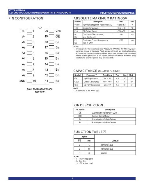
PIN CONFIGURATION<br />
DIR<br />
A1<br />
A2<br />
A3<br />
A4<br />
A5<br />
1<br />
2<br />
3<br />
5<br />
6<br />
A6 7<br />
A7<br />
A8<br />
4<br />
8<br />
9<br />
GND 10<br />
20<br />
19<br />
18<br />
17<br />
16<br />
15<br />
14<br />
13<br />
12<br />
11<br />
SOIC/ SSOP/ QSOP/ TSSOP<br />
TOP VIEW<br />
VCC<br />
OE<br />
B1<br />
B2<br />
B3<br />
B4<br />
B5<br />
B6<br />
B7<br />
B8<br />
ABSOLUTE MAXIMUM RATINGS (1)<br />
Symbol Description Max Unit<br />
VTERM Terminal Voltage <strong>with</strong> Respect to GND –0.5 to +6.5 V<br />
TSTG Storage Temperature –65 to +150 °C<br />
IOUT DC Output Current –50 to +50 mA<br />
IIK Continuous Clamp Current, –50 mA<br />
IOK VI < 0 or VO < 0<br />
ICC Continuous Current through each ±100 mA<br />
ISS VCC or GND<br />
NOTE:<br />
1. Stresses greater than those listed under ABSOLUTE MAXIMUM RATINGS may cause<br />
permanent damage to the device. This is a stress rating only and functional operation<br />
of the device at these or any other conditions above those indicated in the operational<br />
sections of this specification is not implied. Exposure to absolute maximum rating<br />
conditions for extended periods may affect reliability.<br />
CAPACITANCE (TA = +25°C, F = 1.0MHz)<br />
Symbol Parameter (1) Conditions Typ. Max. Unit<br />
CIN Input Capacitance VIN = 0V 4.5 6 pF<br />
COUT Output Capacitance VOUT = 0V 5.5 8 pF<br />
CI/O I/O Port Capacitance VIN = 0V 6.5 8 pF<br />
NOTE:<br />
1. As applicable to the device type.<br />
PIN DESCRIPTION<br />
Pin Names Description<br />
OE<br />
Output Enable Input (Active LOW)<br />
DIR<br />
Direction Control Output<br />
A x<br />
Side A Inputs or 3-State Outputs<br />
B x<br />
Side B Inputs or 3-State Outputs<br />
FUNCTION TABLE (1)<br />
Inputs<br />
OE DIR Outputs<br />
L L B Data to A Bus<br />
L H A Data to B Bus<br />
H X Isolation<br />
NOTE:<br />
1. H = HIGH Voltage Level<br />
X = Don’t Care<br />
L = LOW Voltage Level<br />
2