ICD2051
ICD2051
ICD2051

You also want an ePaper? Increase the reach of your titles
YUMPU automatically turns print PDFs into web optimized ePapers that Google loves.
<strong>ICD2051</strong><br />
Dual Programmable Clock Generator<br />
Features<br />
• Two independent clock outputs ranging from 320 kHz<br />
to 100 MHz<br />
• Individually programmable PLLs use 22-bit serial word<br />
• Low-skew ÷1,÷2, and ÷4 CLKA outputs<br />
• Phase-locked loop oscillator input derived from external<br />
low-frequency reference clock (1 MHz - 25 MHz) or<br />
external crystal (2 MHz - 24 MHz)<br />
• Sophisticated internal loop-filter requires no external<br />
components or manufacturing tweaks as commonly required<br />
with external filters<br />
• Three-state control disables outputs for test purposes<br />
(optional)<br />
• 5V operation<br />
• Low-power, high-speed CMOS technology<br />
• Available in 16-pin SOIC package<br />
Functional Description<br />
The <strong>ICD2051</strong> Programmable Clock Generator offers two fully<br />
user-programmable phase-locked loops in a single package.<br />
The outputs may be changed “on the fly” to any desired frequency<br />
value between 320 kHz and 100 MHz. The <strong>ICD2051</strong><br />
is ideally suited for any design where one or more multiple or<br />
varying frequencies are required, thus replacing more expensive<br />
metal can oscillators.<br />
The capability to dynamically change the output frequency<br />
adds a whole new degree of freedom for the electrical engineer.<br />
Some examples of the uses for this device include: laptop<br />
computers, in which slowing the speed of operation can<br />
mean less power consumption or speeding it up can mean<br />
faster operation; graphics board dot clocks to allow dynamic<br />
synchronization with different brands of monitors or display<br />
formats; and on-board test strategies where the ability to<br />
skew a system’s desired frequency (for example ±10%) allows<br />
worst case evaluations.<br />
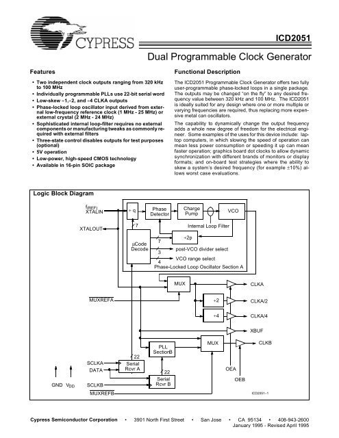
Logic Block Diagram<br />
f (REF)<br />
XTALIN<br />
÷ q<br />
Phase<br />
Detector<br />
Charge<br />
Pump<br />
VCO<br />
XTALOUT<br />
7<br />
Internal Loop Filter<br />
÷2p<br />
7<br />
µCode<br />
Serial<br />
OEB<br />
GND V DD SCLKB<br />
Rcvr B<br />
Decode<br />
3<br />
post-VCO divider select<br />
4<br />
VCO range select<br />
Phase-Locked Loop Oscillator Section A<br />
MUX<br />
MUXREFA ÷2<br />
÷4<br />
PLL<br />
MUX<br />
SectionB<br />
22<br />
SCLKA Serial<br />
DATA Rcvr A<br />
22<br />
OEA<br />
MUXREFB<br />
CLKA<br />
CLKA/2<br />
CLKA/4<br />
XBUF<br />
CLKB<br />
<strong>ICD2051</strong>–1<br />
Cypress Semiconductor Corporation • 3901 North First Street • San Jose • CA 95134 • 408-943-2600<br />
January 1995 - Revised April 1995
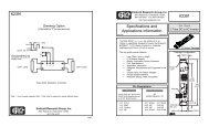
<strong>ICD2051</strong><br />
Pin Configuration<br />
SOIC<br />
Top View<br />
SCLKB<br />
MUXREFB<br />
OEB<br />
GND<br />
f (REF) /XTALIN<br />
XTALOUT<br />
XBUF<br />
CLKB<br />
1<br />
16<br />
2<br />
15<br />
3<br />
14<br />
4<br />
13<br />
5<br />
12<br />
6<br />
11<br />
7<br />
10<br />
8 9<br />
DATA<br />
MUXREFA<br />
OE A<br />
V DD<br />
SCLKA<br />
CLKA/4<br />
CLKA/2<br />
CLKA<br />
<strong>ICD2051</strong>–2<br />
Pin Summary<br />
Name Number Description<br />
SCLKB 1 Serial clock input line for CLKB<br />
MUXREFB 2 MUXREFB = 0, CLKB equals input reference frequency<br />
MUXREFB = 1, CLKB equals programmed frequency<br />
This is used if glitch-free frequency changes are required.<br />
OEB 3 Three-states CLKB outputs when pulled LOW. (Internal pull-up allows for no-connect if three-state<br />
operation is not needed.)<br />
GND 4 Ground<br />
f REF /<br />
5 Reference Oscillator input for all internal phase-locked loops<br />
XTALIN [1]<br />
XTALOUT [1] 6 Oscillator output to a reference crystal.<br />
XBUF 7 Buffered Crystal Oscillator Output<br />
CLKB 8 CLKB Programmable Output<br />
CLKA 9 CLKA Programmable Output<br />
CLKA/2 10 CLKA divided by 2 (low skew)<br />
CLKA/4 11 CLKA divided by 4<br />
SCLKA 12 Serial clock input line for CLKA.<br />
V DD 13 +5V<br />
OEA 14 Three-states CLKA outputs when pulled LOW. (Internal pull-up allows for no-connect if three-state<br />
operation is not needed.)<br />
MUXREFA 15 MUXREFA = 0, CLKA equals input reference frequency<br />
MUXREFA = 1, CLKA equals programmed frequency<br />
This is used if glitch-free frequency changes are required.<br />
DATA 16 Serial data input line for both programmable PLLs<br />
Note:<br />
1. For best accuracy, use a parallel-resonant crystal, assume C LOAD = 17 pF.<br />
2
<strong>ICD2051</strong><br />
General Considerations<br />
Programming the <strong>ICD2051</strong><br />
The desired output frequency is defined via a serial interface,<br />
with a 22-bin number shifted in. The <strong>ICD2051</strong> has two programmable<br />
PLLs (CLKA and CLKB), requiring a 22-bit programming<br />
word (W) to be loaded into each channel independently.<br />
This word contains 5 fields:<br />
Table 1. Programming Word Bit Fields<br />
Field<br />
# of<br />
bits<br />
Notes<br />
Index (I) 4 MSB (Most Significant Bits)<br />
P Counter value (P’) 7<br />
Reserved (R) 1 normally set to logic 1<br />
Mux (M) 3<br />
Q Counter value (Q’) 7 LSB (Least Significant Bits)<br />
The frequency of the programmable oscillator f (VCO) is determined<br />
by these fields as follows:<br />
P’=P−3<br />
Q’=Q−2<br />
f (VCO) =2 x f (REF) x P/Q<br />
where f (REF) =Reference frequency (between 1 MHz − 25 MHz)<br />
The value of f (VCO) must remain between 40 MHz and 120 MHz.<br />
Therefore, for output frequencies below 40 MHz, f (VCO) must be<br />
multiplied up into the required range. To accomplish this, a<br />
post-VCO Divisor is selected by setting the values of the Mux field<br />
(M) as follows:<br />
Table 2. Mux Field (M)<br />
M<br />
Divisor<br />
000 1<br />
001 2<br />
010 4<br />
011 8<br />
100 16<br />
101 32<br />
110 64<br />
111 128<br />
The Index field (I) is used to preset the VCO to an appropriate<br />
range. The value for this field should be should be chosen from<br />
Table 3. (Note that this table is referenced to the VCO frequency<br />
f (VCO) , rather than to the desired output frequency.)<br />
Table 3. Index Field (I)<br />
I<br />
f (VCO) (MHz)<br />
0000 40.0 − 42.5<br />
0001 42.5 − 47l.5<br />
0010 47.5 − 53.5<br />
0011 53.5 − 58.5<br />
0100 58.5 − 62.5<br />
0101 62.5 − 68.5<br />
0110 68.5 − 69.0<br />
0111 69.0 − 82.0<br />
1000 82.0 − 87.0<br />
1001 87.0 − 92.0<br />
1010 92.0 − 92.1<br />
1011 92.1 − 105.0<br />
1100 105.0 − 115.0<br />
1101 115.0 − 120.0<br />
1110 115.0 − 120.0<br />
1111 115.0 − 120.0<br />
If the desired VCO frequency lies on a boundary in the table<br />
(if it is exactly the upper limit of one entry and the lower limit of<br />
the next) then either index value may be used (since both limits<br />
are tested), but we recommend using the higher one.<br />
To assist with these calculations, Cypress/IC Designs provides<br />
BitCalc (Part #ICD/BCALC), a Windows program which<br />
automatically generates the appropriate programming words from<br />
the user’s reference input and desired output frequencies. The software<br />
also assembles the program words for control and power-down<br />
registers. Contact your local Cypress representative for<br />
more information.<br />
Programming Constraints<br />
There are five primary programming constraints the user must<br />
be aware of:<br />
Table 4. Programming Constraints<br />
Parameter Minimum Maximum<br />
f (REF) 1 MHz 25 MHz<br />
f (REF) /Q 200 kHz 1 MHz<br />
f (VCO) 40 MHz 120 MHz<br />
Q 3 129<br />
P 4 130<br />
The constraints have to do with trade-offs between optimum<br />
speed and lowest noise, VCO stability and factors affecting the<br />
loop equation. The factors are listed for completeness sake;<br />
however, by using the BitCalc program all of these constraints<br />
become transparent.<br />
<strong>ICD2051</strong> Programming Example<br />
The following is an example of the calculations BitCalc performs:<br />
3
<strong>ICD2051</strong><br />
Derive the proper programming word for a 39.5 MHz output<br />
frequency, using 14.31818 MHz as the reference frequency:<br />
Since 39.5 MHz
<strong>ICD2051</strong><br />
Maximum Ratings<br />
(Above which the useful life may be impaired. For user guidelines,<br />
not tested.)<br />
Supply Voltage to Ground Potential.................−0.5V to +7.0V<br />
DC Input Voltage ......................................... −0.5V to V DD +0.5V<br />
Storage Temperature ......................................−65°C to +150°C<br />
Max soldering temperature (10 sec) ............................ 260°C<br />
Junction temperature ................................................... 125°C<br />
Operating Conditions<br />
Package power dissipation................................. 525 mWatts<br />
Operating Range<br />
Ambient<br />
Temperature<br />
V DD & AV DD<br />
0°C ϖ T AMBIENT ϖ 70°C 5V ± 5%<br />
Parameter Description Min. Max. Unit<br />
V DD Supply Voltage 4.75 5.25 V<br />
T A Ambient Operating Temperature 0 70 °C<br />
C L Load Capacitance 25 pF<br />
Electrical Characteristics Over the Operating Range<br />
Parameter Description Test Conditions Min. Max. Unit<br />
V OH Output HIGH Voltage I OH = −4.0mA 2.4 V<br />
V OL Output LOW Voltage I OL = 4.0 mA 0.4 V<br />
V IH Input HIGH Voltage Except XTALIN pins 2.0 V<br />
V IL Input LOW Voltage Except XTALIN pins 0.8 V<br />
I IH Input HIGH Current V IN = 5.25V 150 µA<br />
I IL Input LOW Current V IN = 0V −250 µA<br />
I OZ Output Leakage Current Three-state outputs 10 µA<br />
I DD Power Supply Current V DD = V DD max., 100 MHz, V IN = V DD or 0V 15 100 mA<br />
5
<strong>ICD2051</strong><br />
Switching Characteristics Over the Operating Range [2]<br />
Parameter Name Description Min. Max. Unit<br />
Output Frequency 0.320 100 MHz<br />
f (REF) Reference Frequency Reference Oscillator nominal value 1 25 MHz<br />
t (REF) Reference Clock Period t (REF) = 1/f (REF) 40 1000 ns<br />
Duty Cycle<br />
Duty cycle for the output oscillators defined as 40% 60%<br />
t 1A ÷ t 1B<br />
t 2 Output Rise Time Rise time for the outputs into a 25-pF load 3 ns<br />
t 3 Output Fall Time Fall time for the outputs into a 25-pF load 3 ns<br />
t 4 CLKA/2/4 skew Skew delay between the CLKA output and the<br />
2 ns<br />
CLKA/2 and CLKA/4 outputs<br />
t 5 MUXREF Set-Up Time Delay required after MUXREF goes LOW prior t freq1<br />
ns<br />
to starting the SCLK clock line<br />
t 6 SCLK Cycle Time Minimum cycle time for the SCLK clock 2 * t (REF) ns<br />
t 6H SCLK HIGH Time Minimum HIGH time for the SCLK clock t (REF) ns<br />
t 6L SCLK LOW Time Minimum LOW time for the SCLK clock t (REF) ns<br />
t 7<br />
Output Clock Stable Time required for CLKA or CLKB output to become<br />
10 msec<br />
Time<br />
valid after last SCLK clock<br />
t 8 Data Set-Up Time Time required for the data to be valid prior to the 10 ns<br />
rising edge of SCLK<br />
t 9 Data Hold Time Time required for the data to remain valid after 5 ns<br />
the rising edge of SCLK<br />
t 10 Transition Time Time for CLKA or CLKB to go HIGH after assertion<br />
0 t freq1 ns<br />
of MUXREF<br />
t 11 Transition Time Delay of CLKA or CLKB prior to valid t (REF) signal t (REF) /2 3(t (REF) /2) ns<br />
at output<br />
t 12 Transition Time Time for CLKA or CLKB to go HIGH after release<br />
0 t (REF) ns<br />
of MUXREF<br />
t 13 Transition Time Delay of CLKA or CLKB prior to valid new frequency<br />
t freq2 /2 3(t freq2 /2) ns<br />
at output<br />
t 14 Output Disable Time Time for the outputs to go into three-state mode<br />
12 ns<br />
after OE signal assertion<br />
t 15 Output Enable Time Time for the outputs to recover from three-state<br />
12 ns<br />
mode after OE signal goes HIGH<br />
Note:<br />
2. Input capacitance is typically 10 pF, except for the crystal pads.<br />
Switching Waveforms<br />
Duty Cycle Timing<br />
t 1A<br />
t 1B<br />
1.5V 1.5V 1.5V<br />
<strong>ICD2051</strong>–3<br />
6
<strong>ICD2051</strong><br />
Switching Waveforms (continued)<br />
Rise and Fall Times<br />
f (REF)<br />
ALL INPUT<br />
AND OUTPUT<br />
CLOCKS<br />
CLKA/2<br />
CLKA/4<br />
t 2 t 3<br />
90% 90%<br />
10%<br />
10%<br />
t 4<br />
<strong>ICD2051</strong>–4<br />
Serial Programming Timing<br />
MUXREFA<br />
MUXREFB<br />
t 5<br />
22 CLOCKS REQUIRED FOR DATA<br />
SCLKA<br />
SCLKB<br />
t 6H<br />
t 6<br />
t 7<br />
t 6L<br />
t 8<br />
t 9<br />
DATA<br />
DATA VALID<br />
t 10 t 11 t 12<br />
t 13<br />
CLKA<br />
CLKB<br />
t freq1<br />
t (REF)<br />
t freq2<br />
ORIGINAL FREQUENCY REFERENCE FREQUENCY NEW FREQUENCY<br />
<strong>ICD2051</strong>–5<br />
Three-State Timing<br />
OE A<br />
OE B<br />
t 14 t 15<br />
CLKA<br />
CLKB<br />
THREE–STATE OUTPUT<br />
<strong>ICD2051</strong>–6<br />
7
<strong>ICD2051</strong><br />
Test Circuit<br />
DEVICE<br />
UNDER<br />
TEST<br />
V DD<br />
V DD<br />
0.1 µF<br />
CLK out<br />
C LOAD<br />
GND<br />
Ordering Information<br />
Package<br />
Operating<br />
Ordering Code Name Package Type Range<br />
<strong>ICD2051</strong> S1 16−Pin SOIC Commercial [3]<br />
Note:<br />
3. 0°C to +70°C<br />
Document #: 38−00402<br />
Package Diagram<br />
16-Lead Molded SOIC S1<br />
© Cypress Semiconductor Corporation, 1996. The information contained herein is subject to change without notice. Cypress Semiconductor Corporation assumes no responsibility for the use<br />
of any circuitry other than circuitry embodied in a Cypress Semiconductor product. Nor does it convey or imply any license under patent or other rights. Cypress Semiconductor does not authorize<br />
its products for use as critical components in life-support systems where a malfunction or failure may reasonably be expected to result in significant injury to the user. The inclusion of Cypress<br />
Semiconductor products in life-support systems application implies that the manufacturer assumes all risk of such use and in doing so indemnifies Cypress Semiconductor against all charges.