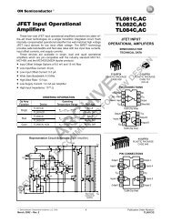
ICD2051
ICD2051
ICD2051

Create successful ePaper yourself
Turn your PDF publications into a flip-book with our unique Google optimized e-Paper software.
<strong>ICD2051</strong><br />
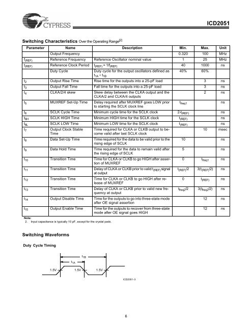
Switching Characteristics Over the Operating Range [2]<br />
Parameter Name Description Min. Max. Unit<br />
Output Frequency 0.320 100 MHz<br />
f (REF) Reference Frequency Reference Oscillator nominal value 1 25 MHz<br />
t (REF) Reference Clock Period t (REF) = 1/f (REF) 40 1000 ns<br />
Duty Cycle<br />
Duty cycle for the output oscillators defined as 40% 60%<br />
t 1A ÷ t 1B<br />
t 2 Output Rise Time Rise time for the outputs into a 25-pF load 3 ns<br />
t 3 Output Fall Time Fall time for the outputs into a 25-pF load 3 ns<br />
t 4 CLKA/2/4 skew Skew delay between the CLKA output and the<br />
2 ns<br />
CLKA/2 and CLKA/4 outputs<br />
t 5 MUXREF Set-Up Time Delay required after MUXREF goes LOW prior t freq1<br />
ns<br />
to starting the SCLK clock line<br />
t 6 SCLK Cycle Time Minimum cycle time for the SCLK clock 2 * t (REF) ns<br />
t 6H SCLK HIGH Time Minimum HIGH time for the SCLK clock t (REF) ns<br />
t 6L SCLK LOW Time Minimum LOW time for the SCLK clock t (REF) ns<br />
t 7<br />
Output Clock Stable Time required for CLKA or CLKB output to become<br />
10 msec<br />
Time<br />
valid after last SCLK clock<br />
t 8 Data Set-Up Time Time required for the data to be valid prior to the 10 ns<br />
rising edge of SCLK<br />
t 9 Data Hold Time Time required for the data to remain valid after 5 ns<br />
the rising edge of SCLK<br />
t 10 Transition Time Time for CLKA or CLKB to go HIGH after assertion<br />
0 t freq1 ns<br />
of MUXREF<br />
t 11 Transition Time Delay of CLKA or CLKB prior to valid t (REF) signal t (REF) /2 3(t (REF) /2) ns<br />
at output<br />
t 12 Transition Time Time for CLKA or CLKB to go HIGH after release<br />
0 t (REF) ns<br />
of MUXREF<br />
t 13 Transition Time Delay of CLKA or CLKB prior to valid new frequency<br />
t freq2 /2 3(t freq2 /2) ns<br />
at output<br />
t 14 Output Disable Time Time for the outputs to go into three-state mode<br />
12 ns<br />
after OE signal assertion<br />
t 15 Output Enable Time Time for the outputs to recover from three-state<br />
12 ns<br />
mode after OE signal goes HIGH<br />
Note:<br />
2. Input capacitance is typically 10 pF, except for the crystal pads.<br />
Switching Waveforms<br />
Duty Cycle Timing<br />
t 1A<br />
t 1B<br />
1.5V 1.5V 1.5V<br />
<strong>ICD2051</strong>–3<br />
6