Electric Vehicle - Design and Implementation Strategies - Icrepq.com
Electric Vehicle - Design and Implementation Strategies - Icrepq.com
Electric Vehicle - Design and Implementation Strategies - Icrepq.com

You also want an ePaper? Increase the reach of your titles
YUMPU automatically turns print PDFs into web optimized ePapers that Google loves.
<strong>Electric</strong> <strong>Vehicle</strong> - <strong>Design</strong> <strong>and</strong> <strong>Implementation</strong> <strong>Strategies</strong><br />
for the Power Train<br />
Rui Santos (1) , Fern<strong>and</strong>o Pais (1) , Carlos Ferreira (1) (2) , Hugo Ribeiro (1) (2) , Pedro Matos (1)<br />
(1) Escola Superior de Tecnologia do Instituto Politécnico de Tomar – Quinta do Contador – Estrada da<br />
Serra, 2300 Tomar, Portugal, phone +351249328150, fax: +351249328187, e-mail: rui_s@zmail.pt,<br />
fmpais@gmail.<strong>com</strong>, granchinho@ipt.pt<br />
(2) Instituto de Tele<strong>com</strong>unicações, Lisboa Portugal, e-mail: cferreira@ipt.pt, hugo@ipt.pt<br />
Abstract. The main objective of this paper is to describe the<br />
solutions encountered during the development of a power<br />
converter <strong>and</strong> its control for an electric traction vehicle.<br />
This paper will focus on strategies <strong>and</strong> construction problems for<br />
the power converter, its protection <strong>and</strong> control of the power train.<br />
Key words: Sliding mode control, electric vehicle,<br />
DC-DC converter.<br />
1. Introduction<br />
Negative environmental impact of the transportation sector<br />
imposes searching for alternative solutions to actual road<br />
vehicles. The vehicle presented in this paper is a prototype<br />
of a pure battery vehicle, which has the advantage of being<br />
a ZEV (zero emissions vehicle). The Fig. 1 shows the<br />
vehicle structure.<br />
The vehicle uses two 11kW@48V DC motors. The option<br />
of operate with low voltage motors is related with safety<br />
concerns; in counterpart this motors needed a high current<br />
value (≈200A).<br />
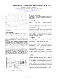
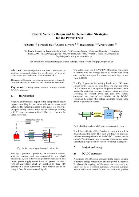
The Fig. 2 presents the building blocks of a DC motor<br />
current control system in closed loop. The objective of the<br />
DC-DC converter is to regulate the power delivered to the<br />
motor; the controller generates a square voltage waveform<br />
according the current error; the gate drive circuit<br />
<strong>com</strong>m<strong>and</strong>s the state of the switches of the DC-DC<br />
converter; the output filter reduce the ripple current in the<br />
motor to provide low losses.<br />
Fig. 2 - Building blocks of a DC motor current control system<br />
The different blocks of Fig. 2 <strong>and</strong> their construction will be<br />
detailed along the paper. This work will focus on strategies<br />
<strong>and</strong> construction problems for the DC-DC converter <strong>and</strong> its<br />
control. This thematic involves power conservation, safety<br />
<strong>and</strong> intuitive response of the system for human interaction.<br />
Fig. 1 - Structure of a pure battery electric vehicle<br />
The Fig. 1 presents a possibility for an electric vehicle,<br />
with two motors, each one associated to one wheel,<br />
providing a system with two independent wheels drive. The<br />
motors power supply <strong>com</strong>es from two power converters<br />
(DC-DC converters) which are supplied by three 12V<br />
batteries in a series connection. These batteries can be recharged<br />
from the mains network (grid).<br />
2. Project <strong>and</strong> design<br />
a) DC-DC converter<br />
A switched DC-DC power converter is the natural solution<br />
to achieve energy conservation <strong>and</strong> low power dissipation.<br />
To choose the topology of the converter is necessary to<br />
know the motor operation dem<strong>and</strong>s. Operation dem<strong>and</strong>s<br />
include vehicle movement forward <strong>and</strong> back with positive
or negative force originated by the motor. For that, four<br />
operation quadrants are defined in a current/voltage plan (I<br />
<strong>and</strong> U respectively) from the point of view of the converter,<br />
or in a torque/angular speed plan (T <strong>and</strong> respectively)<br />
from the point of view of the motor, as displayed in the<br />
Fig. 3, [1].<br />
<br />
<br />
<br />
<br />
<br />
<br />
<br />
<br />
<br />
<br />
<br />
<br />
<br />
<br />
Fig. 3 - Operation in 4 quadrants.<br />
A full bridge converter has been chosen. It operates in the<br />
four quadrants <strong>and</strong> it is possible to control the value <strong>and</strong> the<br />
polarity of the output voltage (V OUT ). The power flow can<br />
have two ways (from the batteries to the load or from the<br />
load to the batteries).<br />
Fig. 5 - Example of gate/source voltage waveforms with time<br />
delay included.<br />
The high currents in cause (200A) <strong>and</strong> the stray<br />
inductances presented in the circuit causes high voltage<br />
transient peaks when the transistors switch. Consequently<br />
the maximum drain source voltage could be exceeded. To<br />
avoid this problems a snubber circuit must be used.<br />
To underst<strong>and</strong> the effects of the stray inductances present<br />
in a real converter, some simulations have been made.<br />
These simulations help to underst<strong>and</strong> the principal causes<br />
of problems <strong>and</strong> also ways to minimise them. The presence<br />
of a stray inductance between the batteries <strong>and</strong> the DC-DC<br />
converter is the major source of problems. The<br />
Fig. 6 presents the simulation circuit.<br />
For safety purposes it was adopted V IN < 50V. In this<br />
voltage range MOSFETS presents the best solution for<br />
switch implementation. The Fig. 4 presents this solution.<br />
V GS3<br />
V GS4<br />
Fig. 6 - Full bridge converter simulation circuit.<br />
Fig. 4 - Full bridge converter.<br />
The switches S 1 /S 4 <strong>and</strong> S 2 /S 3 are actuated by two<br />
<strong>com</strong>plementary signals.<br />
Due the existence of transition times between on <strong>and</strong> off<br />
states of real switches, the short circuit is prevented by the<br />
gate drive circuit, that assures a delay time between the<br />
<strong>com</strong>m<strong>and</strong> S 1 /S 4 <strong>and</strong> S 2 /S 3 signals [2].<br />
The Fig. 5 shows the transistors gate/source voltage<br />
waveforms, S 1 <strong>and</strong> S 2 , with the time delay inserted.<br />
The simulation circuit is a full bridge converter operating<br />
with a D = 0,2 in S 1 /S 4 (D - duty-cycle, t on /(t on +t off )) <strong>and</strong><br />
supplied with 36V. This circuit includes a 100nH stray<br />
inductance, Ls, between the battery <strong>and</strong> the switches; the<br />
load is a RL circuit with 0,05Ω <strong>and</strong> a 11µH inductor<br />
(equivalent model of the used DC motor, when stopped) the<br />
voltage sources V2, V3, V4 <strong>and</strong> V5 are the <strong>com</strong>m<strong>and</strong><br />
signals of the switches.<br />
The Fig. 7 shows the voltage waveform present in S 3 .
Resistances of m present in the circuit (cables,<br />
MOSFETS R DSon <strong>and</strong> inductor resistances) produce heat<br />
<strong>and</strong> losses. Those factors have to be taken in consideration<br />
in the design <strong>and</strong> construction phase, for assuring reliable<br />
operation.<br />
b) Filter<br />
Fig. 7 - Voltage waveform on S 3 .<br />
The spike voltage in S 3 terminals is greater than 46V for<br />
L S =100nH. The solutions for this problem consist in<br />
minimization of the stray inductance values by minimizing<br />
the area inside of the current loop <strong>and</strong> by putting capacitors<br />
in parallel with the voltage source, near the switches. Those<br />
techniques also help minimising EMI (Electro Magnetic<br />
Interference). Beside these techniques it was necessary to<br />
implement snubber circuits for protecting the switches from<br />
overvoltages, Fig. 8.<br />
The motor self-induction coefficient is very low (11H).<br />
Therefore the introduction of an external inductance, L, (in<br />
series with the motor) is indispensable to increase the total<br />
inductance, avoiding high ripple currents. This inductance<br />
must support the output current, I out , without significant<br />
losses. It isn’t possible to use an LC filter, because the<br />
parasitic elements present in a capacitor, Equivalent Series<br />
Resistor (ESR) <strong>and</strong> Equivalent Series Inductance (ESL),<br />
results in high losses.<br />
To design the inductive filter, L, the inductance of the<br />
motor, L M , must be considerated. The total inductance, L T ,<br />
present in the circuit corresponds to the sum of this two<br />
inductances. The Fig. 10 shows the inductive filter <strong>and</strong> the<br />
equivalent circuit of the DC motor. The E represents the<br />
inverse electromotive force produced by the motor.<br />
Fig. 8 - Overvoltage snubber circuits.<br />
Considering the snubber elements, C, R <strong>and</strong> D, <strong>and</strong> S 3<br />
switch, Fig. 9, we have the following principle of<br />
operation: during S 3 conduction time, the voltage on the<br />
capacitor is V IN guaranteed by the resistor R; when S 3 open,<br />
if the drain-source voltage in S 3 is greater than V IN , D<br />
conduces. The overvoltage obtained in C will be dependent<br />
of the stored energy into the stray inductance <strong>and</strong> of the<br />
capacitor value. An approximately value for L S can be<br />
obtained based on the drain-source overvoltage when the<br />
circuit operate without the snubber [3]. In our prototype we<br />
use a 2,2µF for C capacitor <strong>and</strong> 10Ω for R. The Fig. 9<br />
shows the overvoltage attenuation, when the overvoltage<br />
snubber circuit is used (simulation results).<br />
Fig. 10 - Inductive filter <strong>and</strong> the equivalent circuit of the DC<br />
motor.<br />
The current ripple in the motor is given by the equation 1:<br />
v<br />
L<br />
i<br />
L<br />
= t<br />
(1)<br />
L<br />
T<br />
The criteria’s of the L inductance design are related with<br />
the maximum ∆ iL <strong>and</strong> the ∆ T . The ∆ T is dependent of the<br />
transistors switching times, which are defined by the<br />
current control circuit. Consequently, the inductance value<br />
is defined in the control section.<br />
To determinate the inductance L, there was used the<br />
area-product method [4]. For this dimensioning method it<br />
was necessary to define: the ferrite core area, the area that<br />
can be filled with copper wires <strong>and</strong> the size of the core-gap.<br />
The Fig. 11 presents drawings of these dimensions.<br />
Fig. 9 - Voltage waveform on S 3 with overvoltage snubber.
2) Simplicity of design <strong>and</strong> implementation;<br />
3) Capacity to maintain the current error limited in a<br />
pre-defined b<strong>and</strong> (hysteretic b<strong>and</strong>), through<br />
control of the on <strong>and</strong> off states of the switches.<br />
Fig. 11 - Representation of Aw, AE <strong>and</strong> l g for inductance design.<br />
Where:<br />
AE - area of the ferrite core;<br />
Aw - area that can be filled with copper wires;<br />
l g - length of the core-gap.<br />
The number of turns is given by:<br />
LI<br />
B<br />
Lmax<br />
N = (2)<br />
max<br />
A<br />
E<br />
The output voltage of the switched converter could be in<br />
two possible voltage levels: +V IN or -V IN . The sliding mode<br />
controller <strong>com</strong>m<strong>and</strong>s the transition between those two<br />
levels. The difference between the current reference <strong>and</strong> the<br />
real value is used to decide the future state. If the current is<br />
higher than a hysteretic value, i m , the system changes of<br />
state. Consequently the maximum <strong>and</strong> minimum current<br />
value allowed in the DC motor is I ref +∆i m <strong>and</strong> I ref -∆i m ,<br />
making a hysteretic b<strong>and</strong> (I ref ±∆i m ). The current will always<br />
be between these two values. The Fig. 13 shows the<br />
temporary evolution of the motor current to an abrupt<br />
request of the reference signal (I ref ) [5].<br />
Where:<br />
N - Number of turns;<br />
Bmax - Maximum magnetic induction;<br />
ILmax - Maximum current in the inductance;<br />
AE - Area of the ferrite core.<br />
For the values of current in cause there was some difficulty<br />
in finding a ferrite core that allows the sufficient inductance<br />
<strong>and</strong> simultaneously avoid saturation. The inductance<br />
dimensioning is based in E 55/28/21ferrite material.<br />
c) Control<br />
The output current of the converter is the variable to be<br />
controlled. This type of control is better than a voltage<br />
control for two main reasons:<br />
1) It obtains an intuitive correspondence between<br />
throttle control <strong>and</strong> the torque applied. An action<br />
in the throttle control of the vehicle should have<br />
direct correspondence in the torque applied by the<br />
electric machine, as is obtained on an vehicle<br />
equipped with an internal <strong>com</strong>bustion motor;<br />
2) It protects the motor, electronic power converter<br />
<strong>and</strong> mechanics. If the current is not controlled, the<br />
limits of the several electric <strong>and</strong> mechanic<br />
<strong>com</strong>ponents can be surpassed with possible<br />
destruction of the equipment <strong>and</strong> consequently<br />
causing injuries to the passengers.<br />
The current control can be implemented by several<br />
methods. The chosen one was sliding mode control,<br />
essentially due to the following advantages:<br />
1) Well adapted to the discreet characteristic of the<br />
switching signal;<br />
Fig. 12 - Evolution of the motor current in sliding mode control.<br />
In a steady-state operation, the current signal is periodic<br />
with period T. The allowed current change is the hysteretic<br />
b<strong>and</strong> <strong>and</strong> the current changes from I ref -∆i m to I ref +∆i m in the<br />
period ∆t.<br />
The Fig. 14 shows the building blocks diagram of the<br />
control system:<br />
1) The throttle pedal gives the reference signal<br />
(current to be achieved);<br />
2) A current probe gives the signal of the current in<br />
the motor;<br />
3) The error calculator makes the difference between<br />
reference signal <strong>and</strong> the current probe signal;<br />
4) The <strong>com</strong>parator allows a hysteretic error value to<br />
be reached <strong>and</strong> then switches the output value,<br />
generating a <strong>com</strong>m<strong>and</strong> signal;<br />
5) The power converter switches V OUT .
3. <strong>Implementation</strong>s <strong>and</strong> tests<br />
a) <strong>Implementation</strong><br />
The electrical machines used in this project are two LEM<br />
230 motor, manufactured by LMC. They are direct current<br />
(D.C.) motors, with axial brushes, appropriate for traction<br />
in EV’s <strong>and</strong> industrial applications, see Fig 16.<br />
Fig. 13 - Building blocks of the sliding current control.<br />
Sliding current control has variable switching frequency<br />
operation. The maximum switching frequency occurs when<br />
the duty-cycle is 50% <strong>and</strong> the motor is stopped. Using<br />
equation 1, is possible to obtain the maximum switching<br />
frequency, f Smax :<br />
V<br />
IN<br />
f<br />
Smax<br />
= (3)<br />
L<br />
Ti<br />
L<br />
For dimensioning L T a hysteretic current b<strong>and</strong> of 25A was<br />
considered admissible (about 12,5% of the nominal current<br />
of the motor). The maximum frequency considered was<br />
30 kHz (above 20 KHz to avoid audible noise <strong>and</strong> not too<br />
high to avoid elevating to much the switching losses).<br />
Equation 3 gives an L T value of 48H. Consequently the L T<br />
value is 37H.<br />
d) Gate drive circuit<br />
The <strong>com</strong>m<strong>and</strong> signal produced by the sliding control is one<br />
square wave signal. To produce the <strong>com</strong>m<strong>and</strong> signals to the<br />
four transistors of the full bridge (with adequate<br />
gate/source voltages <strong>and</strong> timings) there was necessary the<br />
use a circuit driver. The option is the IC IR2110. This<br />
circuit uses a bootstrap capacitor to produce a voltage<br />
higher than V IN , necessary to actuate the upper side<br />
switches S 1 <strong>and</strong> S 3 . The time delay is produced with logic<br />
circuits <strong>and</strong> RC networks.<br />
Fig. 15 - Motor LEM 230.<br />
Three 12V batteries Optima Yellow Top with 55Ah<br />
capacity were used in a series connection.<br />
The DC/DC power converter contains the MOSFET’s<br />
IRFP2907 (two in parallel for each switch) for 75 V <strong>and</strong><br />
209 A absolute maximum ratings operation.<br />
During the implementation of the DC-DC converter there<br />
were several problems due to the high current value needed<br />
<strong>and</strong> parasitic elements that causes non-desirable effects.<br />
It is important to take in consideration that the current<br />
ripple in the input of the converter is twice the average<br />
output current. Consequently the copper buses used to<br />
solder the transistors <strong>and</strong> build the converter have to be of<br />
considerable dimensions, as can be seen in Fig. 17. They<br />
were attached to a Celeron plate to assure physic stability.<br />
The buses dispositions have been studied to minimize<br />
undesirable stray inductances. Fig. 17 also represents the<br />
low ESR capacitors mounted in parallel with the voltage<br />
source <strong>and</strong> near the switches to reduce stray inductance<br />
effects.<br />
Battery buses<br />
Out buses<br />
Low ESR<br />
capacitors<br />
Fig. 16 - Bottom view of copper buses used for converter<br />
implementation: before <strong>and</strong> after <strong>com</strong>ponent soldering.<br />
Fig. 14 - Half-bridge gate drive circuit.<br />
The fig. 18 shows the 10.000µF electrolytic capacitors, to<br />
provide a low voltage ripple in the buses, <strong>and</strong> snubber<br />
circuits.
Capacitive filter<br />
Capacitive filter<br />
Snubber<br />
Fig. 17 - Converter with snubber <strong>and</strong> capacitive filter.<br />
The design of the L inductance has two <strong>com</strong>peting targets:<br />
minimum size <strong>and</strong> minimum losses. The Ohmic losses vary<br />
with the square of the current (P=R.I 2 ). Due the high values<br />
of current in the inductance (up to 200A) the losses can<br />
easily reach considerable values (in spite of extremely low<br />
resistance, in the order of the m) [6].<br />
(a) CH1 - 25V/div, CH2 - 50A/div<br />
The high diameter of the wire that is needed, make it very<br />
rigid, creating an obstacle to the execution of the coil. The<br />
used strategy is to put several wires in parallel (six wires<br />
were used). With these values <strong>and</strong> considering the areaproduct<br />
method it was necessary to use 5 individual cores<br />
grouped together achieving 33H <strong>and</strong> 2.2m, see Fig 19.<br />
(b) CH1 - 25V/div, CH2 - 25A/div<br />
Fig. 18 - Build inductance<br />
The efficiency of the power converter is relatively high,<br />
with conducting losses being usually higher then switching<br />
ones. The total equivalent resistance presented by the fullbridge,<br />
due to the R DSon of the transistors, is only of about<br />
4.5m. Power dissipation due conducting losses is about<br />
180W at 200A.<br />
4. Experimental results<br />
The Fig. 20 shows the waveforms of the motor current<br />
(triangular waveform) <strong>and</strong> of the output voltage (square<br />
waveform) provided by the optimised converter for three<br />
different duty cycles.<br />
(c) CH1 - 25V/div, CH2 - 50A/div<br />
Fig. 19 - Output voltage converter <strong>and</strong> inductance current for<br />
different duty cycle values; (a) D = 0,3; (b) D = 0,5; (c) D = 0,7.<br />
Fig. 21 show the <strong>com</strong>pleted system implemented <strong>and</strong><br />
mounted in the vehicle.
Fig. 20 - Implemented system in the vehicle.<br />
5. Conclusions<br />
The real implementation of the two power converters <strong>and</strong><br />
the respective current control for two DC motors arises<br />
several questions due to the high currents in cause:<br />
overvoltages at the switching transitions, power dissipation<br />
in cables, EMI <strong>and</strong> filter design. To avoid high current<br />
ripple it was necessary to design <strong>and</strong> construct an<br />
inductance, which is also problematic (due to the some<br />
reasons already referred). All those problems where<br />
surpassed by evaluation of the system limitations, careful<br />
design <strong>and</strong> implementation.<br />
The current control method used allows auto-protection for<br />
some faults: blocked wheels, unequal torque produced by<br />
the two motors when the car is turning (what happens if a<br />
voltage control is used). Another advantage is the intuitive<br />
response of the vehicle obtained when actuating the throttle<br />
control, similar to the internal <strong>com</strong>bustion engine normally<br />
used by the majority of the population.<br />
6. References<br />
Fig. 21 - The vehicle ready to roll.<br />
[1] Palma, J. C., “Accionamentos Electromecânicos de<br />
Velocidade Variável”, Fundação Calouste<br />
Gulbenkian, 1999<br />
[2] Bose, Bimal K., “Power Electronics <strong>and</strong> Variable<br />
Frequency Drives”, IEEE, ISBN 0-7803-1084-5<br />
[3] Mohan, Ned, “Power electronics “ John Wiley &<br />
Sons, Inc. ISBN 0-471-58408-8<br />
[4] Guilherme, Jorge, “Critério de Dimensionamento de<br />
Bobinas e Transformadores”, 2003<br />
[5] Roque, António Eusébio Velho, “Contributos para<br />
um controlo de tracção de um veiculo eléctrico<br />
bimotor”, Master thesis, 2001<br />
[6] Santos, Rui <strong>and</strong> Pais, Fern<strong>and</strong>o, Project Report,<br />
“Desenvolvimento de um Conversor de Potência”,<br />
2006<br />
The objective of this paper is to evaluate solutions for the<br />
power converter <strong>and</strong> control. Other subjects where<br />
addressed in this project: like protection circuits,<br />
mechanics, etc. but they aren’t focused here.<br />
With the present realization, the author’s objective is to<br />
make a small contribute to achieve noise <strong>and</strong> pollution free<br />
cities. The following picture shows the final result of this<br />
project: the “electrical mini”, during a test drive.