Brief introduction to SiC research and development in Korea
Brief introduction to SiC research and development in Korea
Brief introduction to SiC research and development in Korea

Create successful ePaper yourself
Turn your PDF publications into a flip-book with our unique Google optimized e-Paper software.
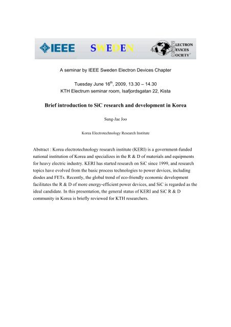
A sem<strong>in</strong>ar by IEEE Sweden Electron Devices Chapter<br />
Tuesday June 16 th , 2009, 13.30 – 14.30<br />
KTH Electrum sem<strong>in</strong>ar room, Isafjordsgatan 22, Kista<br />
<strong>Brief</strong> <strong><strong>in</strong>troduction</strong> <strong>to</strong> <strong>SiC</strong> <strong>research</strong> <strong>and</strong> <strong>development</strong> <strong>in</strong> <strong>Korea</strong><br />
Sung-Jae Joo<br />
<strong>Korea</strong> Electrotechnology Research Institute<br />
Abstract : <strong>Korea</strong> electrotechnology <strong>research</strong> <strong>in</strong>stitute (KERI) is a government-funded<br />
national <strong>in</strong>stitution of <strong>Korea</strong> <strong>and</strong> specializes <strong>in</strong> the R & D of materials <strong>and</strong> equipments<br />
for heavy electric <strong>in</strong>dustry. KERI has started <strong>research</strong> on <strong>SiC</strong> s<strong>in</strong>ce 1999, <strong>and</strong> <strong>research</strong><br />
<strong>to</strong>pics have evolved from the basic process technologies <strong>to</strong> power devices, <strong>in</strong>clud<strong>in</strong>g<br />
diodes <strong>and</strong> FETs. Recently, the global trend of eco-friendly economic <strong>development</strong><br />
facilitates the R & D of more energy-efficient power devices, <strong>and</strong> <strong>SiC</strong> is regarded as the<br />
ideal c<strong>and</strong>idate. In this presentation, the general status of KERI <strong>and</strong> <strong>SiC</strong> R & D<br />
community <strong>in</strong> <strong>Korea</strong> is briefly reviewed for KTH <strong>research</strong>ers.
Sung-Jae Joo, Ph. D.<br />
<strong>Korea</strong> Electrotechnology Research Institute<br />
Energy Efficient Semiconduc<strong>to</strong>rs Research Center,<br />
Advanced Materials Research Division<br />
70 Boolmosangil, ChangWon, GyeongNam, 641-120, <strong>Korea</strong><br />
Phone : +82-55-280-1627, Fax : +82-55-280-1590<br />
E-mail : sj_joo@keri.re.kr<br />
Education<br />
Ph. D. <strong>in</strong> Materials Science & Eng<strong>in</strong>eer<strong>in</strong>g Feb., 2000<br />
Seoul National University, Seoul, <strong>Korea</strong><br />
Thesis : Amorphous Si deposition by ECR-PECVD <strong>and</strong> Analysis<br />
Advisor : Prof. Euijoon Yoon (Dept. of Mater. Sci. & Eng., Seoul Nat’l Univ.)<br />
Master of Eng<strong>in</strong>eer<strong>in</strong>g <strong>in</strong> Materials Science & Eng<strong>in</strong>eer<strong>in</strong>g Feb., 1995<br />
Seoul National University, Seoul, <strong>Korea</strong><br />
Thesis : Low-temp. Si 1-x Ge x heteroepitaxy by ECR-PECVD<br />
Advisor : Prof. Euijoon Yoon (Dept. of Mater. Sci. & Eng., Seoul Nat’l Univ.)<br />
Bachelor of Eng<strong>in</strong>eer<strong>in</strong>g <strong>in</strong> Materials Science & Eng<strong>in</strong>eer<strong>in</strong>g Feb., 1993<br />
Dep’t of Mater. Sci. & Eng., Seoul Nat’l Univ., Seoul, <strong>Korea</strong><br />
Professional Experience<br />
Senior Researcher<br />
Apr., 2006 - Present<br />
<strong>Korea</strong> Electrotechnology Research Institute, ChangWon, GyeongNam, 641-120, <strong>Korea</strong><br />
- <strong>SiC</strong> unit process, process <strong>in</strong>tegration, device fabrication, <strong>and</strong> characterization<br />
Process Eng<strong>in</strong>eer Apr., 2003 - Mar., 2006<br />
System LSI division, Samsung Electronics Co., Ltd., YongIn, 446-711, <strong>Korea</strong><br />
- Process <strong>development</strong> of 1.3M- & 2M-pixel CMOS image sensor devices<br />
Process Eng<strong>in</strong>eer Feb., 2000 - Mar., 2003<br />
Memory R&D division, Hynix Semiconduc<strong>to</strong>r Inc., Ichon, 136-1, <strong>Korea</strong>
- Unit process <strong>development</strong> (Si selective epitaxy & In situ dop<strong>in</strong>g) for DRAM devices employ<strong>in</strong>g<br />
sub-100nm process technology<br />
Recent Publications<br />
• S.-J. Joo, I.-H. Kang, W. Bahng, S.C. Kim, <strong>and</strong> N.-K. Kim, “Fabrication of 1.2 kV Ni/4H-<strong>SiC</strong><br />
junction barrier controlled Schottky diodes with s<strong>in</strong>gle p+ ion implantation process”,<br />
Journal of the <strong>Korea</strong>n Physical Society, Vol. 54, p. 1802, 2009.<br />
• I.-H. Kang, J.Y. Song, S.-J. Joo, W. Bahng, S.C. Kim, <strong>and</strong> N.-K. Kim, “Effect of the dop<strong>in</strong>g<br />
concentration <strong>and</strong> space of both p-grid <strong>and</strong> field limit<strong>in</strong>g r<strong>in</strong>g on 4H-<strong>SiC</strong> junction barrier<br />
Schottky diode with s<strong>in</strong>gle ion implantation process”, Materials Science Forum Vols.<br />
600-603, p. 959, 2009.<br />
• S.-J. Joo, J.Y. Song, I.-H. Kang, W. Bahng, S.C. Kim, <strong>and</strong> N.-K. Kim, “Electrical<br />
characteristics of Ni/Ti/Al ohmic contacts <strong>to</strong> Al-implanted p-type 4H-<strong>SiC</strong>”, Journal of<br />
the <strong>Korea</strong>n Institute of Electrical <strong>and</strong> Electronic Materials Eng<strong>in</strong>eers (<strong>in</strong><br />
<strong>Korea</strong>n), Vol. 21, p. 968, 2008.<br />
• W. Bahng, H.J. Cheong, I.-H. Kang, S.J. Kim, S.C. Kim, S.-J. Joo, <strong>and</strong> N.-K. Kim,<br />
“Modification of surface layer dur<strong>in</strong>g high temperature anneal<strong>in</strong>g <strong>and</strong> its effects on the<br />
<strong>SiC</strong> diode characteristics”, Materials Science Forum Vols. 556-557, p. 595, 2007.