Cyclone II Device Handbook, Chapter 5. DC Characteristics ...
Cyclone II Device Handbook, Chapter 5. DC Characteristics ...
Cyclone II Device Handbook, Chapter 5. DC Characteristics ...

Create successful ePaper yourself
Turn your PDF publications into a flip-book with our unique Google optimized e-Paper software.
<strong>Chapter</strong> <strong>5.</strong> <strong>DC</strong><br />
<strong>Characteristics</strong> & Timing<br />
Specifications<br />
C<strong>II</strong>51005-1.0<br />
Operating<br />
Conditions<br />
<strong>Cyclone</strong> <strong>II</strong> devices are offered in both commercial and industrial<br />
grades. Commercial devices are offered in -6 (fastest), -7, -8 speed grades.<br />
All parameter limits are representative of worst-case supply voltage and<br />
junction temperature conditions. Unless otherwise noted, the parameter<br />
values in this chapter apply to all <strong>Cyclone</strong> <strong>II</strong> devices. AC and <strong>DC</strong><br />
characteristics are specified using the same numbers for both commercial<br />
and industrial grades. All parameters representing voltages are measured<br />
with respect to ground.<br />
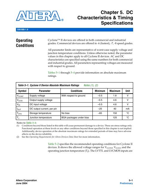
Tables 5–1 through 5–4 provide information on absolute maximum<br />
ratings.<br />
Table 5–1. <strong>Cyclone</strong> <strong>II</strong> <strong>Device</strong> Absolute Maximum Ratings Notes (1), (2)<br />
Symbol Parameter Conditions Minimum Maximum Unit<br />
V CCINT Supply voltage With respect to ground –0.5 1.8 V<br />
V CCIO Output supply voltage –0.5 4.6 V<br />
V IN <strong>DC</strong> input voltage –0.5 4.6 V<br />
I OUT <strong>DC</strong> output current, per pin –25 40 mA<br />
T STG Storage temperature No bias –65 150 °C<br />
T J Junction temperature BGA packages under bias 125 °C<br />
Notes to Table 5–1:<br />
(1) Conditions beyond those listed in this table will cause permanent damage to a device. These are stress ratings only.<br />
Functional operation at these levels or any other conditions beyond those specified in this chapter is not implied.<br />
Additionally, device operation at the absolute maximum ratings for extended periods of time may have adverse<br />
affects on the device reliability.<br />
(2) See the Operating Requirements for Altera <strong>Device</strong>s Data Sheet for more information.<br />
Table 5–2 specifies the recommended operating conditions for <strong>Cyclone</strong> <strong>II</strong><br />
devices. It shows the allowed voltage ranges for V CCINT , V CCIO , and the<br />
operating junction temperature (T J ). The LVTTL and LVCMOS inputs are<br />
Altera Corporation 5–1<br />
June 2004<br />
Preliminary
Operating Conditions<br />
powered by V CCIO only. The LVPECL input buffers on dedicated clock<br />
pins are powered by V CCINT . The SSTL, HSTL, LVDS input buffers are<br />
powered by both V CCINT and V CCIO .<br />
Table 5–2. Recommended Operating Conditions<br />
Symbol Parameter Conditions Minimum Maximum Unit<br />
V CCINT<br />
V CCIO (2)<br />
T J (4)<br />
Supply voltage for internal<br />
logic and input buffers<br />
Supply voltage for output<br />
buffers, 3.3-V operation<br />
Supply voltage for output<br />
buffers, 2.5-V operation<br />
Supply voltage for output<br />
buffers, 1.8-V operation<br />
Supply voltage for output<br />
buffers, 1.5-V operation<br />
Operating junction<br />
temperature<br />
(1) 1.15 1.25 V<br />
(1) 3.00 (3) 3.60 (3) V<br />
(1) 2.375 2.625 V<br />
(1) 1.71 (2) 1.89 V<br />
(1) 1.4 1.6 V<br />
For commercial use 0 85 °C<br />
For industrial use –40 100 °C<br />
Notes to Table 5–2:<br />
(1) The maximum V CC (both V CCIO and V CCINT ) rise time is 100 ms, and V CC must rise monotonically.<br />
(2) The V CCIO range given here spans the lowest and highest operating voltages of all supported I/O standards. The<br />
recommended V CCIO range specific to each of the single-ended I/O standards is given in Table 5–6, and those<br />
specific to the differential standards is given in Table 5–8.<br />
(3) The minimum and maximum values of 3.0 V and 3.6 V, respectively, for V CCIO only applies to the PCI and PCI-X<br />
I/O standards. See Table 5–6 for the voltage range of other I/O standards.<br />
(4) Contact Altera Applications for θ JA and θ JC values.<br />
Table 5–3. <strong>DC</strong> <strong>Characteristics</strong> for User I/O, Dual-Purpose & Dedicated Pins (Part 1 of 2)<br />
Symbol Parameter Conditions Minimum Typical Maximum Unit<br />
V IN Input voltage (1), (2) –0.5 4.0 V<br />
I I<br />
Input pin leakage V I = V CCIOmax to 0 V (3) –10 10 µA<br />
current<br />
V OUT Output voltage 0 V CCIO V<br />
I OZ Tri-stated I/O pin V O = V CCIOmax to 0 V (3) –10 10 µA<br />
leakage current<br />
I CC0<br />
V CC supply current<br />
(standby) (all<br />
memory blocks in<br />
power-down mode)<br />
V I = ground, no load, no<br />
toggling inputs<br />
mA<br />
5–2 Preliminary Altera Corporation<br />
<strong>Cyclone</strong> <strong>II</strong> <strong>Device</strong> <strong>Handbook</strong>, Volume 1 June 2004
<strong>DC</strong> <strong>Characteristics</strong> & Timing Specifications<br />
Table 5–3. <strong>DC</strong> <strong>Characteristics</strong> for User I/O, Dual-Purpose & Dedicated Pins (Part 2 of 2)<br />
Symbol Parameter Conditions Minimum Typical Maximum Unit<br />
R CONF<br />
Value of I/O pin pullup<br />
resistor before<br />
and during<br />
configuration<br />
V CCIO = 3.0 V (4) 20 50 kΩ<br />
V CCIO = 2.375 V (4) 30 80 kΩ<br />
V CCIO = 1.71 V (4) 60 150 kΩ<br />
Notes to Table 5–3:<br />
(1) All pins, including dedicated inputs, clock, I/O, and JTAG pins, may be driven before V CCINT and V CCIO are<br />
powered.<br />
(2) The minimum <strong>DC</strong> input is –0.5 V. During transitions, the inputs may undershoot to –2.0 V or overshoot to the<br />
voltages shown in Table 5–4, based on input duty cycle for input currents less than 100 mA. The overshoot is<br />
dependent upon duty cycle of the signal. The <strong>DC</strong> case is equivalent to 100% duty cycle.<br />
(3) This value is specified for normal device operation. The value may vary during power-up. This applies for all<br />
V CCIO settings (3.3, 2.5, 1.8, and 1.5 V).<br />
(4) Pin pull-up resistance values will lower if an external source drives the pin higher than V CCIO .<br />
Table 5–4 shows the maximum V IN overshoot voltage and the<br />
dependency on the duty cycle of the input signal. See Table 5–3 for more<br />
information.<br />
Table 5–4. V IN Overshoot Voltage for All Input Buffers<br />
Maximum V IN (V)<br />
Input Signal Duty Cycle<br />
4.0 100% (<strong>DC</strong>)<br />
4.1 90%<br />
4.2 50%<br />
4.3 30%<br />
4.4 17%<br />
4.5 10%<br />
Altera Corporation Preliminary 5–3<br />
June 2004 <strong>Cyclone</strong> <strong>II</strong> <strong>Device</strong> <strong>Handbook</strong>, Volume 1
Operating Conditions<br />
Single-Ended I/O Standards<br />
Tables 5–6 and 5–7 provide operating condition information when using<br />
single-ended I/O standards with <strong>Cyclone</strong> <strong>II</strong> devices. Table 5–5 provides<br />
descriptions for the voltage and current symbols used in Tables 5–6 and<br />
5–7.<br />
Table 5–<strong>5.</strong> Voltage & Current Symbol Definitions<br />
V CCIO<br />
V REF<br />
V IL<br />
V IH<br />
V OL<br />
V OH<br />
I OL<br />
I OH<br />
V TT<br />
Symbol<br />
Definition<br />
Supply voltage for single-ended inputs and for output drivers<br />
Reference voltage for setting the input switching threshold<br />
Input voltage that indicates a low logic level<br />
input voltage that indicates a high logic level<br />
Output voltage that indicates a low logic level<br />
Output voltage that indicates a high logic level<br />
Output current condition under which V OL is tested<br />
Output current condition under which V OH is tested<br />
Voltage applied to a resistor termination as specified by<br />
HSTL and SSTL standards<br />
Table 5–6. Recommended Operating Conditions for User I/O Pins Using Single-Ended I/O Standards (Part<br />
1 of 2) Note (1)<br />
I/O Standard<br />
3.3-V LVTTL and<br />
LVCMOS<br />
2.5-V LVTTL and<br />
LVCMOS<br />
1.8-V LVTTL and<br />
LVCMOS<br />
V CCIO (V) V REF (V) V IL (V) V IH (V)<br />
Min Nom Max Min Nom Max Max Min<br />
3.135 3.3 3.465 0.8 1.7<br />
2.375 2.5 2.625 0.7 1.7<br />
1.710 1.8 1.890 0.35 × V CCIO 0.65 × V CCIO<br />
1.5-V LVCMOS 1.425 1.5 1.575 0.35 × V CCIO 0.65 × V CCIO<br />
PCI and PCI-X 3.000 3.3 3.600 0.3 × V CCIO 0.5 × V CCIO<br />
SSTL-2 class I 2.375 2.5 2.625 1.19 1.25 1.31 V REF – 0.18 V REF + 0.18<br />
SSTL-2 class <strong>II</strong> 2.375 2.5 2.625 1.19 1.25 1.31 V REF – 0.18 V REF + 0.18<br />
SSTL-18 class I 1.7 1.8 1.9 0.833 0.9 0.969 V REF – 0.125 V REF + 0.125<br />
SSTL-18 class <strong>II</strong> 1.7 1.8 1.9 0.833 0.9 0.969 V REF – 0.125 V REF + 0.125<br />
1.8-V HSTL class I 1.71 1.8 1.89 0.85 0.9 0.95 V REF – 0.1 V REF + 0.1<br />
5–4 Preliminary Altera Corporation<br />
<strong>Cyclone</strong> <strong>II</strong> <strong>Device</strong> <strong>Handbook</strong>, Volume 1 June 2004
<strong>DC</strong> <strong>Characteristics</strong> & Timing Specifications<br />
Table 5–6. Recommended Operating Conditions for User I/O Pins Using Single-Ended I/O Standards (Part<br />
2 of 2) Note (1)<br />
I/O Standard<br />
V CCIO (V) V REF (V) V IL (V) V IH (V)<br />
Min Nom Max Min Nom Max Max Min<br />
1.8-V HSTL class <strong>II</strong> 1.71 1.8 1.89 0.85 0.9 0.95 V REF – 0.1 V REF + 0.1<br />
1.5-V HSTL class I 1.425 1.5 1.575 0.71 0.75 0.79 V REF – 0.1 V REF + 0.1<br />
1.5-V HSTL class <strong>II</strong> 1.425 1.5 1.575 0.71 0.75 0.79 V REF – 0.1 V REF + 0.1<br />
Note to Table 5–6:<br />
(1) Nominal values (Nom) are for T A = 25° C, V CCINT = 1.2 V, and V CCIO = 1.5, 1.8, 2.5, and 3.3 V.<br />
Table 5–7. <strong>DC</strong> <strong>Characteristics</strong> of User I/O Pins Using Single-Ended Standards (Part 1 of 2) Note (1)<br />
I/O Standard<br />
Current Drive<br />
Strength Setting<br />
(mA)<br />
Test Conditions<br />
Voltage Thresholds<br />
I OL (mA) I OH (mA) Maximum V OL (V) Minimum V OH (V)<br />
3.3-V LVTTL and<br />
LVCMOS<br />
2.5-V LVTTL and<br />
LVCMOS<br />
1.8-V LVTTL and<br />
LVCMOS<br />
4 4 –4 0.4 2.4<br />
8 8 –8<br />
12 12 –12<br />
16 16 –16<br />
20 20 –20<br />
24 24 –24<br />
4 4 –4 0.4 V CCIO – 0.4<br />
8 8 –8<br />
12 12 –12<br />
16 16 –16<br />
2 2 –2 0.4 V CCIO – 0.4<br />
4 4 –4<br />
6 6 –6<br />
8 8 –8<br />
10 10 –10<br />
12 12 –12<br />
1.5-V LVCMOS 2 2 –2 0.25 × V CCIO 0.75 × V CCIO<br />
4 4 –4<br />
6 6 –6<br />
8 8 –8<br />
PCI and PCI-X 1.5 –0.5 0.1 × V CCIO 0.9 × V CCIO<br />
Altera Corporation Preliminary 5–5<br />
June 2004 <strong>Cyclone</strong> <strong>II</strong> <strong>Device</strong> <strong>Handbook</strong>, Volume 1
Operating Conditions<br />
Table 5–7. <strong>DC</strong> <strong>Characteristics</strong> of User I/O Pins Using Single-Ended Standards (Part 2 of 2) Note (1)<br />
I/O Standard<br />
Current Drive<br />
Strength Setting<br />
(mA)<br />
Test Conditions<br />
Voltage Thresholds<br />
I OL (mA) I OH (mA) Maximum V OL (V) Minimum V OH (V)<br />
SSTL-2 class I 8 8 –8 V TT – 0.57 V TT + 0.57<br />
12 12 –12<br />
SSTL-2 class <strong>II</strong> 16 16 –16 V TT – 0.76 V TT + 0.76<br />
20 20 –20<br />
24 24 –24<br />
SSTL-18 class I 4 4 –4 V TT – 0.475 V TT + 0.475<br />
6 6 –6<br />
8 8 –8<br />
10 10 –10<br />
12 12 –12<br />
SSTL-18 class <strong>II</strong> 8 8 –8 0.28 V CCIO – 0.28<br />
16 16 –16<br />
18 18 –18<br />
1.8-V HSTL class I 4 4 –4 0.4 V CCIO – 0.4<br />
6 6 –6<br />
8 8 –8<br />
10 10 –10<br />
12 12 –12<br />
1.8-V HSTL class <strong>II</strong> 16 16 –16 0.4 V CCIO – 0.4<br />
18 18 –18<br />
20 20 –20<br />
1.5-V HSTL class I 4 4 –4 0.4 V CCIO – 0.4<br />
6 6 –6<br />
8 8 –8<br />
10 10 –10<br />
12 12 –12<br />
1.5V HSTL class <strong>II</strong> 16 16 –16 0.4 V CCIO – 0.4<br />
Note to Table 5–7:<br />
(1) The values in this table are based on the conditions listed in Tables 5–2 and 5–6.<br />
5–6 Preliminary Altera Corporation<br />
<strong>Cyclone</strong> <strong>II</strong> <strong>Device</strong> <strong>Handbook</strong>, Volume 1 June 2004
<strong>DC</strong> <strong>Characteristics</strong> & Timing Specifications<br />
Differential I/O Standards<br />
Figure 5–1 shows the required connections for LVDS, mini-LVDS, and<br />
RSDS. The RSDS and mini-LVDS I/O standards are only supported on<br />
output pins. The receiver side requires a 100-Ω resistor in line with the<br />
LVDS standard. The transmit side requires three additional resistors to<br />
shift the voltage level at the two single-ended 3.3-V LVTTL output pins to<br />
meet LVDS, RSDS, and mini-LVDS voltage requirements. The same<br />
resistor network is used on the transmitter side for all three differential<br />
standards.<br />
Figure 5–1. LVDS, mini-LVDS & RSDS Applications Using <strong>Cyclone</strong> <strong>II</strong><br />
<strong>Cyclone</strong> <strong>II</strong> <strong>Device</strong><br />
Transmitting <strong>Device</strong><br />
txout +<br />
txout -<br />
rxin +<br />
100 Ω<br />
rxin -<br />
<strong>Cyclone</strong> <strong>II</strong><br />
Logic<br />
Array<br />
txout +<br />
120 Ω<br />
120 Ω<br />
txout -<br />
rxin +<br />
170 Ω 100 Ω<br />
rxin -<br />
Receiving <strong>Device</strong><br />
Input Buffer<br />
Output Buffer<br />
Figure 5–2 shows the receiver input waveforms for all differential I/O<br />
standards (LVDS, LVPECL, differential 1.5-V HSTL class I and <strong>II</strong>,<br />
differential 1.8-V HSTL class I and <strong>II</strong>, differential SSTL-2 class I and <strong>II</strong>, and<br />
differential SSTL-18 class I and <strong>II</strong>).<br />
Altera Corporation Preliminary 5–7<br />
June 2004 <strong>Cyclone</strong> <strong>II</strong> <strong>Device</strong> <strong>Handbook</strong>, Volume 1
Operating Conditions<br />
Figure 5–2. Receiver Input Waveforms for Differential I/O Standards<br />
Single-Ended Waveform<br />
Positive Channel (p) = V IH<br />
V ID (1)<br />
V ICM (2)<br />
Negative Channel (n) = V IL<br />
Ground<br />
Differential Waveform (Mathematical Function of Positive & Negative Channel)<br />
V ID (1)<br />
0 V<br />
V ID (1)<br />
p − n (3)<br />
Notes to Figure 5–2:<br />
(1) V ID is the differential input voltage. V ID = |p – n|.<br />
(2) V ICM is the input common mode voltage. V ICM = (p – n)/2.<br />
(3) The p – n waveform is a function of the positive channel (p) and the negative channel (n).<br />
5–8 Preliminary Altera Corporation<br />
<strong>Cyclone</strong> <strong>II</strong> <strong>Device</strong> <strong>Handbook</strong>, Volume 1 June 2004
<strong>DC</strong> <strong>Characteristics</strong> & Timing Specifications<br />
Table 5–8 shows the recommended operating conditions for user I/O<br />
pins with differential I/O standards.<br />
Table 5–8. Recommended Operating Conditions for User I/O Pins Using Differential Signal I/O Standards<br />
I/O<br />
V CCIO (V) V ID (V) (1) V ICM (V) V IL (V) V IH (V)<br />
Standard<br />
Min Nom Max Min Nom Max Min Nom Max Min Max Min Max<br />
LVDS 2.375 2.5 2.625 0.1 0.1 1.25 1.8<br />
mini-LVDS<br />
(2)<br />
2.375 2.5 2.625<br />
RSDS (2) 2.375 2.5 2.625<br />
LVPECL (3) 3.135 3.3 3.465 0.1 0.6 0.95 0 2.2 2.1 2.88<br />
Differential<br />
1.5-V HSTL<br />
class I<br />
and <strong>II</strong> (4)<br />
Differential<br />
1.8-V HSTL<br />
class I<br />
and <strong>II</strong> (4)<br />
Differential<br />
SSTL-2<br />
class I<br />
and <strong>II</strong> (5)<br />
Differential<br />
SSTL-18<br />
class I<br />
and <strong>II</strong> (5)<br />
1.425 1.5 1.575 0.2 V CCIO<br />
+ 0.6<br />
0.68 0.9 V REF<br />
– 0.1<br />
1.71 1.8 1.89 V REF<br />
– 0.1<br />
2.375 2.5 2.625 0.36 V CCIO<br />
+ 0.6<br />
1.7 1.8 1.9 0.25 V CCIO<br />
+ 0.6<br />
0.5 ×<br />
V CCIO<br />
– 0.2<br />
0.5 ×<br />
V CCIO<br />
– 0.2<br />
0.5 × 0.5 ×<br />
V CCIO V CCIO<br />
+ 0.2<br />
0.5 × 0.5 ×<br />
V CCIO V CCIO<br />
+ 0.2<br />
V REF<br />
– 0.1<br />
V REF<br />
– 0.1<br />
V REF<br />
+ 0.1<br />
V REF<br />
+ 0.1<br />
V REF<br />
+ 0.1<br />
V REF<br />
+ 0.1<br />
Notes to Table 5–8:<br />
(1) Refer to the High-Speed Differential Interfaces in <strong>Cyclone</strong> <strong>II</strong> <strong>Device</strong>s chapter in Volume 1 of the <strong>Cyclone</strong> <strong>II</strong> <strong>Device</strong><br />
<strong>Handbook</strong> for measurement conditions on V ID .<br />
(2) The RSDS and mini-LVDS I/O standards are only supported on output pins.<br />
(3) The LVPECL I/O standard is only supported on clock input pins. This I/O standard is not supported on output<br />
pins.<br />
(4) The differential 1.8-V and 1.5-V HSTL I/O standards are only supported on clock input pins and PLL output clock<br />
pins.<br />
(5) The differential SSTL-18 and SSTL-2 I/O standards are only supported on clock input pins and PLL output clock<br />
pins.<br />
Figure 5–3 shows the transmitter output waveforms for all supported<br />
differential output standards (LVDS, mini-LVDS, RSDS, differential 1.5-V<br />
HSTL class I and <strong>II</strong>, differential 1.8-V HSTL class I and <strong>II</strong>, differential<br />
SSTL-2 class I and <strong>II</strong>, and differential SSTL-18 class I and <strong>II</strong>).<br />
Altera Corporation Preliminary 5–9<br />
June 2004 <strong>Cyclone</strong> <strong>II</strong> <strong>Device</strong> <strong>Handbook</strong>, Volume 1
Operating Conditions<br />
Figure 5–3. Transmitter Output Waveforms for Differential I/O Standards<br />
Single-Ended Waveform<br />
V OD (1)<br />
Positive Channel (p) = V OH<br />
V OCM (2)<br />
Negative Channel (n) = V OL<br />
Ground<br />
Differential Waveform (Mathematical Function of Positive & Negative Channel)<br />
V OD (1)<br />
0 V<br />
V OD (1)<br />
p − n (3)<br />
Notes to Figures 5–2 & 5–3:<br />
(1) V OD is the output differential voltage. V OD = |p – n|.<br />
(2) V OCM is the output common mode voltage. V OCM = (p – n)/2.<br />
(3) The p – n waveform is a function of the positive channel (p) and the negative channel (n).<br />
Table 5–9 shows the <strong>DC</strong> characteristics for user I/O pins with differential<br />
I/O standards.<br />
Table 5–9. <strong>DC</strong> <strong>Characteristics</strong> for User I/O Pins Using Differential I/O Standards (Part 1 of 2) Note (1)<br />
I/O Standard<br />
V OD (mV) ∆V OD (mV) V OCM (V) V OH (V) V OL (V)<br />
Min Typ Max Min Max Min Typ Max Min Max Min Max<br />
LVDS 247 600 50 1.125 1.25 1.375<br />
mini-LVDS (2) 300 600 50 1 1.2 1.4<br />
RSDS (2) 100 200 600 0.5 1.2 1.5<br />
Differential 1.5-V<br />
HSTL class I<br />
and <strong>II</strong> (3)<br />
Differential 1.8-V<br />
HSTL class I<br />
and <strong>II</strong> (3)<br />
Differential<br />
SSTL-2 class I<br />
(4)<br />
V CCIO<br />
– 0.4<br />
V CCIO<br />
– 0.4<br />
V TT +<br />
0.57<br />
0.4<br />
0.4<br />
V TT –<br />
0.57<br />
5–10 Preliminary Altera Corporation<br />
<strong>Cyclone</strong> <strong>II</strong> <strong>Device</strong> <strong>Handbook</strong>, Volume 1 June 2004
<strong>DC</strong> <strong>Characteristics</strong> & Timing Specifications<br />
Table 5–9. <strong>DC</strong> <strong>Characteristics</strong> for User I/O Pins Using Differential I/O Standards (Part 2 of 2) Note (1)<br />
I/O Standard<br />
Differential<br />
SSTL-2 class <strong>II</strong><br />
(4)<br />
Differential<br />
SSTL-18 class I<br />
(4)<br />
Differential<br />
SSTL-18 class <strong>II</strong><br />
(4)<br />
V OD (mV) ∆V OD (mV) V OCM (V) V OH (V) V OL (V)<br />
Min Typ Max Min Max Min Typ Max Min Max Min Max<br />
0.5 ×<br />
V CCIO<br />
–<br />
0.125<br />
0.5 ×<br />
V CCIO<br />
–<br />
0.125<br />
0.5 × 0.5 ×<br />
V CCIO V CCIO<br />
+<br />
0.125<br />
0.5 × 0.5 ×<br />
V CCIO V CCIO<br />
+<br />
0.125<br />
V TT +<br />
0.76<br />
V TT +<br />
0.475<br />
V CCIO<br />
– 0.28<br />
V TT –<br />
0.76<br />
V TT –<br />
0.475<br />
0.28<br />
Notes to Table 5–9:<br />
(1) The LVPECL I/O standard is only supported on clock input pins. This I/O standard is not supported on output<br />
pins.<br />
(2) The RSDS and mini-LVDS I/O standards are only supported on output pins.<br />
(3) The differential 1.8-V HSTL and differential 1.5-V HSTL I/O standards are only supported on clock input pins and<br />
PLL output clock pins.<br />
(4) The differential SSTL-18 and SSTL-2 I/O standards are only supported on clock input pins and PLL output clock<br />
pins.<br />
<strong>DC</strong><br />
<strong>Characteristics</strong><br />
for Different Pin<br />
Types<br />
Table 5–10 shows which types of pins that support bus hold circuitry.<br />
Table 5–10. Bus Hold Support<br />
Pin Type<br />
Bus Hold<br />
I/O pins using single-ended I/O standards Yes<br />
I/O pins using differential I/O standards No<br />
Dedicated clock pins<br />
No<br />
JTAG<br />
No<br />
Configuration pins<br />
No<br />
Altera Corporation Preliminary 5–11<br />
June 2004 <strong>Cyclone</strong> <strong>II</strong> <strong>Device</strong> <strong>Handbook</strong>, Volume 1
<strong>DC</strong> <strong>Characteristics</strong> for Different Pin Types<br />
Table 5–11 specifies the bus hold parameters for general I/O pins.<br />
Table 5–11. Bus Hold Parameters Note (1)<br />
V CCIO Level<br />
Parameter<br />
Conditions<br />
1.8 V 2.5 V 3.3 V<br />
Unit<br />
Min Max Min Max Min Max<br />
Bus-hold low, sustaining<br />
current<br />
Bus-hold high, sustaining<br />
current<br />
Bus-hold low, overdrive<br />
current<br />
Bus-hold high, overdrive<br />
current<br />
V IN ><br />
V IL (maximum)<br />
V IN <<br />
V IL (minimum)<br />
30 50 70 µA<br />
–30 –50 –70 µA<br />
0 V < V IN < V CCIO 200 300 500 µA<br />
0 V < V IN < V CCIO –200 –300 –500 µA<br />
Bus-hold trip point (2) 0.68 1.07 0.7 1.7 0.8 2.0 V<br />
Notes to Table 5–11:<br />
(1) There is no specification for bus-hold at V CCIO = 1.5 V for the HSTL I/O standard.<br />
(2) The bus-hold trip points are based on calculated input voltages from the JEDEC standard.<br />
Table 5–12 shows the <strong>Cyclone</strong> <strong>II</strong> device pin capacitance for different I/O<br />
pin types.<br />
Table 5–12. <strong>Device</strong> Capacitance Note (1)<br />
Symbol Parameter Typical Unit<br />
C IO Input capacitance for user I/O pin (2) pF<br />
C LVDS Input capacitance for dual-purpose<br />
LVDS/user I/O pin<br />
(2) pF<br />
C VREF<br />
C DPCLK<br />
Input capacitance for dual-purpose<br />
VREF and user I/O pin.<br />
Input capacitance for dual-purpose<br />
DPCLK and user I/O pin.<br />
(2) pF<br />
(2) pF<br />
C CLK Input capacitance for clock pin. (2) pF<br />
Notes to Table 5–12:<br />
(1) Capacitance is sample-tested only. Capacitance is measured using time-domain<br />
reflectometry (TDR). Measurement accuracy is within ±0.5 pF.<br />
(2) This specification will be available in a future version of the data sheet.<br />
5–12 Preliminary Altera Corporation<br />
<strong>Cyclone</strong> <strong>II</strong> <strong>Device</strong> <strong>Handbook</strong>, Volume 1 June 2004
<strong>DC</strong> <strong>Characteristics</strong> & Timing Specifications<br />
Table 5–13 shows the specification for ESD for all <strong>Cyclone</strong> <strong>II</strong> pins.<br />
Table 5–13. ESD Protection<br />
Symbol Parameter Maximum Unit<br />
ESD HBM Human body model 1,000 V<br />
ESD CDM Charged device model 500 V<br />
Charged device model for PLL<br />
power pins and dedicated clocks<br />
1, 3, 9, and 11<br />
300 V<br />
Power<br />
Consumption<br />
Designers can calculate the power usage for their design using the Altera<br />
power calculator and the simulation-based power estimation feature in<br />
the Quartus ® <strong>II</strong> software.<br />
The interactive power calculator is typically used prior to designing the<br />
FPGA in order to get a magnitude estimate of the device power. The<br />
Quartus <strong>II</strong> software simulation-based power estimation feature allows<br />
designers to apply test vectors against their design for more accurate<br />
power consumption modeling.<br />
In both cases, these calculations should only be used as an estimation of<br />
power, not as a specification.<br />
f<br />
Contact Altera Applications for information on the <strong>Cyclone</strong> <strong>II</strong> power<br />
calculator.<br />
Altera Corporation Preliminary 5–13<br />
June 2004 <strong>Cyclone</strong> <strong>II</strong> <strong>Device</strong> <strong>Handbook</strong>, Volume 1
Timing Specifications<br />
<strong>Cyclone</strong> <strong>II</strong> devices require a certain amount of power-up current to<br />
successfully power up because of the nature of the leading-edge process<br />
on which they are fabricated. Table 5–14 will show the maximum powerup<br />
current required to power up a <strong>Cyclone</strong> <strong>II</strong> device after device<br />
characterization has been performed.<br />
Table 5–14. <strong>Cyclone</strong> <strong>II</strong> Power-Up Current (I CCINT ) Requirements<br />
<strong>Device</strong><br />
Maximum Power-Up Current<br />
Requirement<br />
Unit<br />
EP2C5 (1) mA<br />
EP2C8 (1) mA<br />
EP2C20 (1) mA<br />
EP2C35 (1) mA<br />
EP2C50 (1) mA<br />
EP2C70 (1) mA<br />
Note to Table 5–14:<br />
(1) This specification will be available in a future version of the data sheet.<br />
Designers should select power supplies and regulators that can supply<br />
this amount of current when designing with <strong>Cyclone</strong> <strong>II</strong> devices. This<br />
specification is for commercial operating conditions. Measurements were<br />
performed with an isolated <strong>Cyclone</strong> <strong>II</strong> device on the board. Decoupling<br />
capacitors were not used in this measurement. To factor in the current for<br />
decoupling capacitors, sum up the current for each capacitor using the<br />
following equation:<br />
I = C (dV/dt)<br />
The exact amount of current that will be consumed varies according to the<br />
process, temperature, and power ramp rate. The duration of the I CCINT<br />
power-up requirement depends on the V CCINT voltage supply rise time.<br />
Altera recommends using the <strong>Cyclone</strong> <strong>II</strong> Power Calculator to estimate the<br />
user-mode I CCINT consumption and then select power supplies or<br />
regulators based on the higher value.<br />
Timing<br />
Specifications<br />
The DirectDrive technology and MultiTrack interconnect ensure<br />
predictable performance, accurate simulation, and accurate timing<br />
analysis across all <strong>Cyclone</strong> <strong>II</strong> device densities and speed grades. This<br />
section describes and specifies the performance, internal, external, and<br />
PLL timing specifications.<br />
5–14 Preliminary Altera Corporation<br />
<strong>Cyclone</strong> <strong>II</strong> <strong>Device</strong> <strong>Handbook</strong>, Volume 1 June 2004
<strong>DC</strong> <strong>Characteristics</strong> & Timing Specifications<br />
This section shows the timing models for <strong>Cyclone</strong> <strong>II</strong> devices. Commercial<br />
devices will meet this timing over the commercial temperature range.<br />
Industrial devices will meet this timing over the industrial temperature<br />
range. All specifications are representative of worst-case supply voltage<br />
and junction temperature conditions.<br />
The preliminary timing model will be added into a future revision of this<br />
Data Sheet.<br />
Preliminary & Final Timing Specifications<br />
Timing models can have either preliminary or final status. The Quartus <strong>II</strong><br />
software issues an informational message during the design compilation<br />
if the timing models are preliminary. Table 5–15 shows the status of the<br />
<strong>Cyclone</strong> <strong>II</strong> device timing models.<br />
Preliminary status means the timing model is subject to change. Initially,<br />
timing numbers are created using simulation results, process data, and<br />
other known parameters. These tests are used to make the preliminary<br />
numbers as close to the actual timing parameters as possible.<br />
Final timing numbers are based on actual device operation and testing.<br />
These numbers reflect the actual performance of the device under worstcase<br />
voltage and junction temperature conditions.<br />
Table 5–1<strong>5.</strong> <strong>Cyclone</strong> <strong>II</strong> <strong>Device</strong> Timing Model Status<br />
<strong>Device</strong> Preliminary Final<br />
EP2C5<br />
EP2C8<br />
EP2C20<br />
EP2C35<br />
EP2C50<br />
EP2C70<br />
v<br />
v<br />
v<br />
v<br />
v<br />
v<br />
Altera Corporation Preliminary 5–15<br />
June 2004 <strong>Cyclone</strong> <strong>II</strong> <strong>Device</strong> <strong>Handbook</strong>, Volume 1
PLL Timing Specifications<br />
PLL Timing<br />
Specifications<br />
Table 5–16 describes the <strong>Cyclone</strong> <strong>II</strong> PLL specifications. <strong>Cyclone</strong> <strong>II</strong> PLLs<br />
will function within the commercial junction temperature range from 0°<br />
to 85° C.<br />
Table 5–16. PLL Specifications Note (1)<br />
Symbol Parameter Min Max Unit<br />
f IN Input frequency (-6 speed grade) 1<strong>5.</strong>625 464 MHz<br />
Input frequency (-7 speed grade) 1<strong>5.</strong>625 428 MHz<br />
Input frequency (-8 speed grade) 1<strong>5.</strong>625 387 MHz<br />
f IN DUTY Input clock duty cycle 40 60 %<br />
f IN JITTER Input clock period jitter 200 ps<br />
f OUT_EXT (external PLL PLL output frequency (-6 speed grade) 1<strong>5.</strong>625 320 MHz<br />
clock output)<br />
PLL output frequency (-7 speed grade) 1<strong>5.</strong>625 320 MHz<br />
PLL output frequency (-8 speed grade) 1<strong>5.</strong>625 275 MHz<br />
f OUT (to global clock) PLL output frequency (-6 speed grade) 1<strong>5.</strong>625 402.5 MHz<br />
PLL output frequency (-7 speed grade) 1<strong>5.</strong>625 320 MHz<br />
PLL output frequency (-8 speed grade) 1<strong>5.</strong>625 275 MHz<br />
t OUT DUTY<br />
Duty cycle for external clock output (when<br />
set to 50%)<br />
45 55 %<br />
t JITTER (2) Period jitter for external clock output ps<br />
t LOCK (3)<br />
Time required to lock from end of device<br />
1 ms<br />
configuration<br />
f VCO (4) PLL internal VCO operating range 500 1,000 MHz<br />
Notes to Table 5–16:<br />
(1) These numbers are preliminary and pending silicon characterization.<br />
(2) The t JITTER specification for the PLL[2..1]_OUT pins are dependent on the I/O pins in its VCCIO bank, how many<br />
of them are switching outputs, how much they toggle, and whether or not they use programmable current<br />
strength.<br />
(3) Lock circuit operation is not guaranteed below –20° C.<br />
(4) If the design enables divide by 2, a 300- to 499-MHz internal VCO frequency is available.<br />
High Speed I/O Timing Specifications<br />
Since LVDS, mini-LVDS, and RSDS data communication is source<br />
synchronous, timing analysis is different than other I/O standards. The<br />
high-speed I/O signal is based on skew between the data and the clock<br />
signal.<br />
Designers should also consider board skew, cable skew, and clock jitter in<br />
their calculation. This section provides details on high-speed I/O<br />
standards timing parameters in <strong>Cyclone</strong> <strong>II</strong> devices.<br />
5–16 Preliminary Altera Corporation<br />
<strong>Cyclone</strong> <strong>II</strong> <strong>Device</strong> <strong>Handbook</strong>, Volume 1 June 2004
<strong>DC</strong> <strong>Characteristics</strong> & Timing Specifications<br />
Table 5–17 defines the parameters of the timing diagram shown in<br />
Figure 5–4.<br />
Table 5–17. High-Speed I/O Timing Definitions<br />
Parameter Symbol Description<br />
High-speed I/O<br />
data rate<br />
HSIODR<br />
Period TUI Time unit interval.<br />
TUI = 1/HSIODR.<br />
Channel-tochannel<br />
skew<br />
TCCS<br />
High-speed receiver and transmitter input<br />
and output data rate.<br />
The timing difference between the fastest<br />
and slowest output edges, including t CO<br />
variation and clock skew. The clock is<br />
included in the TCCS measurement.<br />
TCCS = TUI – SW – (2 × RSKM)<br />
Sampling window SW The period of time during which the data<br />
must be valid in order for you to capture it<br />
correctly. Sampling window is the sum of<br />
the setup time, hold time, and jitter. The<br />
window of t SU + t H is expected to be<br />
centered in the sampling window.<br />
SW = TUI – TCCS – (2 × RSKM)<br />
Receiver input<br />
skew margin<br />
RSKM<br />
RSKM is defined by the total margin left<br />
after accounting for the sampling window<br />
and TCCS. The RSKM equation is:<br />
RSKM = (TUI – SW – TCCS) / 2<br />
Figure 5–4. High-Speed I/O Timing Diagram<br />
External<br />
Input Clock<br />
Time Unit Interval (TUI)<br />
Internal Clock<br />
Receiver<br />
Input Data<br />
TCCS<br />
RSKM<br />
Sampling Window (SW)<br />
RSKM<br />
TCCS<br />
Figure 5–5 shows the high-speed I/O timing budget.<br />
Altera Corporation Preliminary 5–17<br />
June 2004 <strong>Cyclone</strong> <strong>II</strong> <strong>Device</strong> <strong>Handbook</strong>, Volume 1
PLL Timing Specifications<br />
Figure 5–<strong>5.</strong> High-Speed I/O Timing Budget Note (1)<br />
Internal Clock Period<br />
Note to Figure 5–5:<br />
(1) The equation for the high-speed I/O timing budget is:<br />
period = TCCS + RSKM + SW + RSKM.<br />
0.5 × TCCS RSKM<br />
SW<br />
RSKM 0.5 × TCCS<br />
Table 5–18 shows the RSDS timing budget for <strong>Cyclone</strong> <strong>II</strong> devices at<br />
170 Mbps. RSDS is supported for transmitting from <strong>Cyclone</strong> <strong>II</strong> devices.<br />
<strong>Cyclone</strong> <strong>II</strong> devices can not receive RSDS data because the devices are<br />
intended for applications where they will be driving display drivers.<br />
<strong>Cyclone</strong> <strong>II</strong> devices support a maximum RSDS data rate of 170 Mbps using<br />
DDIO registers. The maximum internal clock frequency when designing<br />
for RSDS is 85 MHz.<br />
Table 5–18. RSDS Transmitter Timing Specification<br />
Symbol<br />
HSIODR<br />
Conditions<br />
Using DDIO<br />
registers (1)<br />
-6 Speed Grade -7 Speed Grade -8 Speed Grade<br />
Min Typ Max Min Typ Max Min Typ Max<br />
Unit<br />
31.25 170 31.25 170 31.25 170 Mbps<br />
Period <strong>5.</strong>88 <strong>5.</strong>88 <strong>5.</strong>88 ns<br />
TCCS 1.68 1.68 1.68 ns<br />
SW (2) 4.00 4.00 4.00 ns<br />
RSKM (3) 0.10 0.10 0.10 ns<br />
Notes to Table 5–18:<br />
(1) The minimum data rate is limited by 2 × f IN (minimum) for the PLL specifications shown in Table 5–16.<br />
(2) This is how large the sampling window (sum of t SU , t H , and t JITTER ) can be at the receiving device. The <strong>Cyclone</strong> <strong>II</strong><br />
device is a transmitter only for the RSDS I/O standard.<br />
(3) The RSKM is assumed to be 100 ps for a calculated sampling window. RSKM is a system parameter determined by<br />
the designer.<br />
In order to determine the transmitter timing requirements, RSDS receiver<br />
timing requirements on the other end of the link must be taken into<br />
consideration. RSDS receiver timing parameters are typically defined as<br />
5–18 Preliminary Altera Corporation<br />
<strong>Cyclone</strong> <strong>II</strong> <strong>Device</strong> <strong>Handbook</strong>, Volume 1 June 2004
<strong>DC</strong> <strong>Characteristics</strong> & Timing Specifications<br />
t SU and t H requirements. Therefore, the transmitter timing parameter<br />
specifications are t CO (minimum) and t CO (maximum). Refer to Figure 5–5<br />
for the timing budget.<br />
The AC timing requirements for RSDS are shown in Figure 5–6.<br />
Figure 5–6. RSDS Transmitter Clock to Data Relationship<br />
Transmitter<br />
Clock (<strong>5.</strong>88 ns)<br />
Channel-to-Channel<br />
Skew (1.68 ns)<br />
At transmitter<br />
tx_data[11..0]<br />
Transmitter<br />
Valid<br />
Data<br />
Transmitter<br />
Valid<br />
Data<br />
At receiver<br />
rx_data[11..0]<br />
Valid<br />
Data<br />
Valid<br />
Data<br />
Total<br />
Skew<br />
t SU (2 ns)<br />
t H (2 ns)<br />
Table 5–19 shows the mini-LVDS transmitter timing budget for <strong>Cyclone</strong> <strong>II</strong><br />
devices at 170 Mbps. <strong>Cyclone</strong> <strong>II</strong> devices can not receive mini-LVDS data<br />
because the devices are intended for applications where they will be<br />
Altera Corporation Preliminary 5–19<br />
June 2004 <strong>Cyclone</strong> <strong>II</strong> <strong>Device</strong> <strong>Handbook</strong>, Volume 1
PLL Timing Specifications<br />
driving display drivers. A maximum mini-LVDS data rate of 170 Mbps is<br />
supported for <strong>Cyclone</strong> <strong>II</strong> devices using DDIO registers. The maximum<br />
internal clock frequency when designing for mini-LVDS is 85 MHz.<br />
Table 5–19. mini-LVDS Transmitter Timing Specification<br />
Symbol<br />
HSIODR<br />
Conditions<br />
Using DDIO<br />
registers (1)<br />
-6 Speed Grade -7 Speed Grade -8 Speed Grade<br />
Min Typ Max Min Typ Max Min Typ Max<br />
Unit<br />
31.25 170 31.25 170 31.25 170 Mbps<br />
Period <strong>5.</strong>88 <strong>5.</strong>88 <strong>5.</strong>88 ns<br />
TCCS 0.388 0.388 0.388 ns<br />
SW (2) <strong>5.</strong>292 <strong>5.</strong>292 <strong>5.</strong>292 ns<br />
RSKM (3) 0.10 0.10 0.10 ns<br />
Notes to Table 5–19:<br />
(1) The minimum data rate is limited by 2 × f IN (minimum) for the PLL specifications shown in Table 5–16.<br />
(2) This is how large the sampling window (sum of t SU , t H , and t JITTER ) can be at the receiving device. The <strong>Cyclone</strong> <strong>II</strong><br />
device is a transmitter only for mini-LVDS.<br />
(3) RSKM assumed to be 100 ps for calculated SW. RSKM is a system parameter determined by the designer.<br />
In order to determine the transmitter timing requirements, mini-LVDS<br />
receiver timing requirements on the other end of the link must be taken<br />
into consideration. mini-LVDS receiver timing parameters are typically<br />
defined as t SU and t H requirements. Therefore, the transmitter timing<br />
parameter specifications are t CO (minimum) and t CO (maximum). Refer to<br />
Figure 5–5 for the timing budget.<br />
The AC timing requirements for mini-LVDS are shown in Figure 5–7.<br />
Figure 5–7. mini-LVDS Transmitter AC Timing Specification<br />
LVDSCLK[]n<br />
LVDSCLK[]p<br />
LVDS[]p<br />
LVDS[]n<br />
TUI<br />
t SU (1) t H (2)<br />
t SU (1) t H (2)<br />
Notes to Figure 5–7:<br />
(1) The data setup time, t SU , is 0.225 × TUI.<br />
(2) The data hold time, t H , is 0.225 × TUI.<br />
5–20 Preliminary Altera Corporation<br />
<strong>Cyclone</strong> <strong>II</strong> <strong>Device</strong> <strong>Handbook</strong>, Volume 1 June 2004
<strong>DC</strong> <strong>Characteristics</strong> & Timing Specifications<br />
Table 5–20 shows the LVDS timing budget for <strong>Cyclone</strong> <strong>II</strong> devices.<br />
<strong>Cyclone</strong> <strong>II</strong> devices support LVDS receivers at data rates up to 805 Mbps<br />
and LVDS transmitters at data rates up to 622 Mbps.<br />
Table 5–20. LVDS Timing Specification<br />
Symbol<br />
Conditions<br />
-6 Speed Grade -7 Speed Grade -8 Speed Grade<br />
Min Typ Max Min Typ Max Min Typ Max<br />
HSIODR 10 156.25 622 156.25 622 156.25 530 Mbps<br />
(1)<br />
8 125 622 125 622 125 530 Mbps<br />
7 125 622 125 622 125 530 Mbps<br />
4 62.5 622 62.5 622 62.5 530 Mbps<br />
2 31.25 622 31.25 622 31.25 530 Mbps<br />
1 (2) 1<strong>5.</strong>625 311 1<strong>5.</strong>625 311 1<strong>5.</strong>625 265 Mbps<br />
Period 1.608 1.608 1.886 ns<br />
TCCS 200 200 230 ps<br />
SW (3) 800 800 920 ps<br />
RSKM 304 304 368 ps<br />
Notes to Table 5–20:<br />
(1) The minimum data rate is limited by 2 × f IN (minimum) for the PLL specifications shown in Table 5–16.<br />
(2) The PLL must divide down the input clock frequency to have the internal clock frequency meet the specification<br />
shown in Table 5–16.<br />
(3) These values assume 400 ps of PLL jitter for the SW parameter.<br />
Unit<br />
Altera Corporation Preliminary 5–21<br />
June 2004 <strong>Cyclone</strong> <strong>II</strong> <strong>Device</strong> <strong>Handbook</strong>, Volume 1
PLL Timing Specifications<br />
5–22 Preliminary Altera Corporation<br />
<strong>Cyclone</strong> <strong>II</strong> <strong>Device</strong> <strong>Handbook</strong>, Volume 1 June 2004