Multi-pole Microstrip Directional Filters for Multiplexing ... - inaoe
Multi-pole Microstrip Directional Filters for Multiplexing ... - inaoe
Multi-pole Microstrip Directional Filters for Multiplexing ... - inaoe

Create successful ePaper yourself
Turn your PDF publications into a flip-book with our unique Google optimized e-Paper software.
<strong>Multi</strong>-<strong>pole</strong> <strong>Microstrip</strong> <strong>Directional</strong> <strong>Filters</strong> <strong>for</strong> <strong>Multi</strong>plexing Applications<br />
Humberto Lobato-Morales, Alonso Corona-Chávez, J. Luis Olvera-Cervantes, D.V.B.<br />
Murthy<br />
Instituto Nacional de Astrofísica, Óptica y Electrónica, INAOE<br />
humbertolm@ieee.org<br />
Abstract<br />
Theory and experiment of multi-<strong>pole</strong> microstrip<br />
directional filters <strong>for</strong> multiplexing networks are presented<br />
in this paper. Conventional microstrip directional filters<br />
present only a single-<strong>pole</strong> filter response. By applying<br />
stopband filter theory, two Butterworth microstrip<br />
directional filters are designed and tested. The desired<br />
multi-<strong>pole</strong> filter response is achieved by cascading two or<br />
more similar single stages connected by immitance<br />
inverters. These types of directional filters are ideal<br />
candidates <strong>for</strong> multiplexing applications since they<br />
present the characteristics of easy implementation and the<br />
capacity of a modular concept. Moreover, a flat response<br />
is obtained along the passband due to the multi-<strong>pole</strong> filter<br />
behavior.<br />
1. Introduction<br />
The principles of combining or separating frequency<br />
diverse microwave channels <strong>for</strong> interfacing with a single<br />
port antenna system have been known <strong>for</strong> many years [1].<br />
With the growth of satellite communication systems, the<br />
greatest technical advances were made in multiplexing<br />
structures [1]. Modern communication systems require<br />
multi-band operation, which includes mobile telephony<br />
communication systems, radiolocation and satellite links.<br />
Several configurations have been employed <strong>for</strong><br />
multiplexing network structures, such as hybrid-coupled,<br />
circulator-coupled, manifold filters and directional filters<br />
multiplexers [1].<br />
Hybrid-coupled multiplexers present the advantages<br />
of multi-<strong>pole</strong> filter response, and a modular concept;<br />
however, it makes use of two identical filters and two<br />
hybrids per channel, which adds physical size and weight<br />
compared to other approaches. <strong>Multi</strong>plexing by using<br />
circulators requires only one standard filter, and it allows<br />
a modular concept, but, as long as the signals must pass<br />
through circulators, they suffer extra loss per trip; also,<br />
they only present one way signal flow at the time. A<br />
manifold multiplexer requires only one filter per channel<br />
to operate, and is capable of realizing optimum<br />
per<strong>for</strong>mance in terms of insertion loss, amplitude and<br />
group delay; however, it presents a complex design, a<br />
high time consuming tuning process, and it is not<br />
amenable to flexible frequency channels, i.e., change of a<br />
channel frequency requires a new multiplexer design. A<br />
directional filter based multiplexer requires only one filter<br />
per channel, is simple to tune and is amenable <strong>for</strong> a<br />
modular concept; however, it is restricted to the use of a<br />
single <strong>pole</strong> filter response [1] – [4].<br />
In this paper, the theory, design and implementation<br />
of multi-<strong>pole</strong> response microstrip directional filters <strong>for</strong><br />
multiplexing structures is presented. It has been proved<br />
that cascading more than one stage operating at the same<br />
frequency it is possible to achieve a multi-<strong>pole</strong> response,<br />
maintaining its main advantages of easy design,<br />
implementation and management in a modular concept.<br />
This paper is organized as follows: Section 2 presents<br />
the theory of directional filters; Section 3 shows the<br />
multi-<strong>pole</strong> theory applied to directional filters; the design<br />
and construction of multi-<strong>pole</strong> directional filters are<br />
presented in Section 4; the concept of a multiplexer based<br />
on multi-<strong>pole</strong> directional filters is shown in Section 5;<br />
conclusions are discussed in Section 6.<br />
2. <strong>Microstrip</strong> <strong>Directional</strong> Filter design<br />
A <strong>Directional</strong> Filter is a four-port device having a<br />
bandpass response between ports 1 and 4 (S 41 ), and its<br />
complementary rejectband response between ports 1 and<br />
2 (S 21 ), no power is transmitted to port 3, and none is<br />
reflected to port 1 [2] – [6]. Fig. 1 shows a microstrip<br />
directional filter designed with two half-wavelength (λ g /2)<br />
resonators [6].<br />
The 3-dB bandwidth <strong>for</strong> this structure can be<br />
obtained in terms of its quality factor Q between ports 1<br />
and 4 [2]<br />
1 f2 − f1<br />
= , (1)<br />
Q f0<br />
where f 1 and f 2 are the lower and upper -3 dB cutoff<br />
frequencies and f 0 is the central frequency [2].
operating at the same frequency, by immitance inverters<br />
(quarter wavelength lines) between each stage. Fig. 3<br />
shows a three-<strong>pole</strong> directional filter. Each stage<br />
corresponds to a single conventional directional filter.<br />
Figure 3. Three-<strong>pole</strong> directional filter composed<br />
by single stages connected by 90° lines.<br />
Figure 1. <strong>Microstrip</strong> directional filter.<br />
The mechanism of directionality in this filter is<br />
explained by using the superposition principle based on<br />
the length of the lines between the coupling points (Fig.<br />
1) T 1 and T 2 (90°), and points T 3 and T 4 (270°) [2], [3]: at<br />
the operation frequency, excitation of ports 1 and 4 at the<br />
points T 1 and T 4 with V/2 (even mode) amplitude waves,<br />
and excitation of ports 1 and 4 at the same points with<br />
waves of amplitude V/2 and –V/2 respectively (odd<br />
mode), are equivalent to the excitation of port 1 with a V<br />
amplitude wave. The resonator on the right side is excited<br />
by the even mode excitation of ports 1 and 4, and reflects<br />
V/2 amplitude waves at ports 1 and 4. The left resonator is<br />
excited by the odd mode excitation, reflecting waves of<br />
amplitude –V/2 and V/2 at ports 1 and 4 respectively.<br />
There<strong>for</strong>e, the amplitude of the wave at port 4 is V, while<br />
at ports 1, 2 and 3 is zero. At frequencies outside<br />
resonance, the signals entering into port 1 pass<br />
unattenuated to port 2 [2] – [4].<br />
<strong>Directional</strong> filters can be arranged to <strong>for</strong>m<br />
multiplexing networks (separation or combination of<br />
different channels). Fig. 2 shows a multiplexing structure<br />
composed by four directional filters operating at different<br />
channels each one [2]. The structure can also act as a<br />
channel combiner if all arrows are reversed [2].<br />
The correspondent multi-<strong>pole</strong> design procedure is<br />
based on narrow stopband filter theory [7]. Due to the<br />
directional characteristic of these filters, a stopband<br />
response is obtained between ports 1 and 2, and its<br />
complementary bandpass response is achieved between<br />
ports 1 and 4, so each stage of the multi-<strong>pole</strong> directional<br />
filter, from ports 1 to 2 (Fig. 1), acts as a notch resonator.<br />
By cascading several stages connected by immitance<br />
inverters (90° lines in Fig. 3) it is possible to achieve a<br />
multi-<strong>pole</strong> stopband response between ports 1 and 2 of the<br />
overall structure, consequently, its complementary multi<strong>pole</strong><br />
bandpass response is generated between ports 1 and<br />
4 of the complete configuration.<br />
A general approach <strong>for</strong> the design of narrow<br />
stopband filters is based on reactance slope parameters of<br />
the resonators [7]. Based on a lowpass prototype, the<br />
transition from bandstop filter design is effected by<br />
frequency mapping [7]<br />
Ωc Ω=<br />
FBW , (2)<br />
ω/ ω0 −ω0<br />
/ ω<br />
ω0 = ωω<br />
1 2<br />
, (3)<br />
2 1<br />
FBW ω −<br />
= ω , (4)<br />
ω0<br />
where Ω is the normalized frequency of the lowpass<br />
prototype, Ω c is its cutoff, ω 0 is the midband frequency<br />
and FBW represents the fractional bandwidth of the<br />
bandstop filter limited by ω 1 and ω 2 [7]. An equivalent<br />
model <strong>for</strong> the n-<strong>pole</strong> stopband filter is shown in Fig. 4 [7].<br />
Figure 2. A <strong>Multi</strong>plexing structure composed by<br />
directional filters.<br />
3. <strong>Multi</strong>-<strong>pole</strong> directional filters<br />
Conventionally, the main drawback of these<br />
directional filters is that they are limited to only two<br />
resonators, which gives a single-<strong>pole</strong> filter response. This<br />
degrades the stopband and limits the bandwidth to very<br />
narrow responses [1] – [6]. However, resonator scalability<br />
is possible due to the cascading of directional filters,<br />
Figure 4. Equivalent model of an n-<strong>pole</strong><br />
stopband filter.
The parameters Z 0 and Z U from Fig. 4 correspond to<br />
the terminating and characteristic immitance inverter<br />
impedances respectively [7]. All the circuit parameters<br />
including inductances L i and capacitances C i can be<br />
defined in terms of the lowpass prototype elements [7].<br />
For the schematic model of Fig. 4 [7]:<br />
2<br />
⎛Z<br />
⎞<br />
U 1<br />
⎜ ⎟ = , (5)<br />
⎝ Z0 ⎠ gg<br />
0 n + 1<br />
2<br />
1 ⎛Z<br />
⎞<br />
U<br />
g0<br />
0 i<br />
0<br />
ω0 i 0 iΩc<br />
xi<br />
= ω L = = Z ⎜ ⎟<br />
, (6)<br />
C ⎝ Z ⎠ g FBW<br />
<strong>for</strong> i = 1 to n,<br />
where g i are the element values of the lowpass prototype.<br />
The parameters x i are the reactance slopes of the shunt<br />
series resonators [7], which are related to the 3-dB<br />
bandwidth (Δf 3dB ) of each stage by<br />
x<br />
Z<br />
f Q<br />
. (7)<br />
2 2<br />
0<br />
= =<br />
0<br />
Δf3dB<br />
Equation (7) is very useful because it relates the<br />
normalized reactance slope parameter to the frequency<br />
response of a stopband resonator [7]. In a single<br />
directional filter (stage), Eq. (7) is applied to the<br />
transmission S 21 response, due to the stopband resonator<br />
nature of this structure between ports 1 and 2, and it can<br />
be easily obtained by EM simulation or measurement [7].<br />
Fig. 5 plots the S 21 response of a single stage <strong>for</strong><br />
normalized x i parameter extraction.<br />
Figure 5. S 21<br />
frequency response <strong>for</strong> x i<br />
parameter<br />
extraction.<br />
4. Design of <strong>Multi</strong>-<strong>pole</strong> directional filters<br />
A two-<strong>pole</strong> Butterworth directional filter is designed<br />
<strong>for</strong> GSM applications at f 0 = 0.858 GHz and FBW = 0.086<br />
(8.6 %) [8]. Table 1 tabulates the correspondent lowpass<br />
design parameters [7] and the resultant normalized x i<br />
parameters based on (5) and (6). For maximum<br />
transmission and optimum per<strong>for</strong>mance, Z 0 = Z U = 50 Ω<br />
[7]. The filter is implemented on a Rogers RO4003C<br />
substrate with ε r = 3.38 and thickness h = 1.524 mm [9].<br />
Fig. 6 shows the first single stage of the directional filter.<br />
Table 1. Lowpass parameters <strong>for</strong> Butterworth<br />
filter, c<br />
= 1 [7], and x i<br />
values.<br />
x x<br />
1<br />
2<br />
g 0 g 1 g 2 g 3<br />
Z Z<br />
1.0000 1.4142 1.4142 1.0000 8.1987 8.1987<br />
Figure 6. One stage of the proposed Butterworth<br />
directional filter.<br />
The first stage of the multi-<strong>pole</strong> Butterworth<br />
directional filter is a symmetrical structure composed by<br />
open loop resonators of 22 mm x 28 mm, and coupled to<br />
the corresponding lines by interdigital coupling, which<br />
consists of 37 fingers of 0.2 mm width and 2.2 mm<br />
length, separated by 0.2 mm gap between them. The line<br />
which connects T 1 and T 2 coupling points is of 53 mm<br />
length (90°), and the upper line, which connects T 3 and T 4<br />
coupling points, is a meandered line of 159 mm length<br />
(270°). All the lines are of 3.4 mm width <strong>for</strong> 50 Ω<br />
characteristic impedances.<br />
By using a full wave EM simulator [10], the structure<br />
is analyzed in terms of its S parameters. Eq. (7) is used <strong>for</strong><br />
the calculation of the required normalized x i values, which<br />
can be achieved by varying the resonator couplings.<br />
The structure is optimized to achieve the normalized<br />
x 1 value of 8.1987 by varying the length of the interdigital<br />
fingers. Fig. 7 shows the variation of the normalized x i<br />
versus length of the fingers <strong>for</strong> the stage of Fig. 6; it is<br />
observable that larger the interdigital fingers, larger the<br />
resonator coupling, and consequently, lower the<br />
normalized x i parameter value, according to Eq. (7).<br />
The optimized simulated frequency responses of the<br />
stage of Fig. 6 are plotted in Fig 8.<br />
It can be appreciated from Fig. 8 that good rejection<br />
level in S 21 (near -30 dB) is achieved by the structure at f 0 .<br />
The complementary S 41 curve, allows total transmission at<br />
f 0 . No reflection (S 11 ) is generated to port 1, and port 3<br />
(S 31 ) remains isolated (below -20 dB).<br />
0<br />
0
while the measured bandwidth results of 6.9 %. The<br />
experimental frequency of operation shifted 23 MHz<br />
down due to fabrication tolerances. The experimental<br />
bandpass insertion loss at the central frequency is of -0.9<br />
dB. S 11 and S 31 curves are below -15 dB in simulations and<br />
measurements.<br />
Figure 7. Normalized x i<br />
parameters versus length<br />
of interdigital fingers.<br />
(a)<br />
Figure 8. Frequency response of the stage of<br />
Fig. 6.<br />
From Table 1, it is noticeable that the complete<br />
multi-<strong>pole</strong> structure is symmetrical (x 1 /Z 0 = x 2 /Z 0 ), so the<br />
stage of Fig. 6 is repeated and cascaded by immitance<br />
inverters (90° lines) to <strong>for</strong>m the multi-<strong>pole</strong> directional<br />
filter. Fig. 9 shows the complete structure of the proposed<br />
two-<strong>pole</strong> Butterworth directional filter.<br />
Figure 9. Two-<strong>pole</strong> Butterworth directional filter<br />
<strong>for</strong> 850 GSM applications.<br />
The proposed filter is implemented, and tested using<br />
an Agilent PNA-series vector network analyzer (VNA)<br />
E8361A. The simulated and experimental S 21 and S 41<br />
responses are plotted in Fig. 10(a), and the simulated and<br />
experimental S 11 and S 31 curves are plotted in Fig. 10(b).<br />
From Fig. 10, it is noticeable that responses are in<br />
agreement. The overall simulated bandwidth is of 7.2 %,<br />
(b)<br />
Figure 10. Simulated and experimental frequency<br />
responses <strong>for</strong> the 850 GSM directional filter,<br />
(a) S 21<br />
and S 41<br />
, (b) S 11<br />
and S 31<br />
.<br />
A second two-<strong>pole</strong> Butterworth directional filter is<br />
designed <strong>for</strong> operation in the Radiolocation and Space<br />
Research band [8], from f 1 = 1.215 GHz to f 2 = 1.3 GHz,<br />
with f 0 = 1.257 GHz, and FBW = 0.068 (6.8 %), on the<br />
same Rogers substrate. The lowpass filter g i parameters<br />
are the same as <strong>for</strong> the 850 GSM filter. Due to the<br />
symmetry of the model and the structure, the resulting<br />
normalized reactance slope parameters are x 1 /Z 0 = x 2 /Z 0 =<br />
10.4553. The filter is designed by following the same<br />
procedure as <strong>for</strong> the 850 GSM-band filter. Fig. 11 shows<br />
the two-<strong>pole</strong> directional filter <strong>for</strong> the Radiolocation and<br />
Space Research band.
Figure 11. Two-<strong>pole</strong> Butterworth directional filter<br />
<strong>for</strong> radiolocation and space research<br />
applications.<br />
The filter of Fig. 11 is composed by open loop<br />
resonators coupled by 27 interdigital fingers of width 0.2<br />
mm, length 2.2 mm, and 0.2 mm gap between them. The<br />
overall length of each resonator loop is 76 mm. The<br />
length of the lines that connect the coupling points T 1 – T 2<br />
and T 3 – T 4 are 38 mm and 114 mm respectively. The<br />
lines that connect both the stages are of 38 mm length. All<br />
the lines are of 3.56 mm width to achieve 50 Ω<br />
impedances.<br />
The filter is implemented and tested <strong>for</strong> the<br />
frequency response. Simulated and experimental S 21 and<br />
S 41 parameters are plotted in Fig. 12(a), the correspondent<br />
S 11 and S 31 curves are shown in Fig. 12(b).<br />
From Fig. 12, it is clearly observable that simulated<br />
and experimental curves are in good agreement. The<br />
overall bandwidth of the simulated filter is of 7.1 %.<br />
From measurements, the overall bandwidth results of 6.7<br />
%. A frequency shift down of 9 MHz is observed <strong>for</strong> the<br />
measured response. Insertion losses at the passband (S 41 )<br />
are of -0.8 dB. S 11 and S 31 parameters are below -14 dB.<br />
5. <strong>Multi</strong>plexer with directional filters<br />
(a)<br />
(b)<br />
Figure 12. Simulated and experimental<br />
responses <strong>for</strong> the filter of Fig. 11, (a) S 21<br />
and S 41<br />
,<br />
(b) S 11<br />
and S 31<br />
.<br />
To implement a multiplexing network structure,<br />
directional filters are cascaded, as shown in Fig. 2. The<br />
designed two <strong>pole</strong> directional filters are connected in a<br />
modular concept to <strong>for</strong>m a multiplexing network which<br />
operates at 850 GSM (filter 1), and Radiolocation and<br />
Space Research bands (1.26 GHz, filter 2). Photograph of<br />
the two-band multiplexer is shown in Fig. 13. The<br />
stopband filter response <strong>for</strong> both the bands is obtained at<br />
port 2. The 850 GSM band is received at port 4 (S 41 ); the<br />
Radiolocation and Space Research band is obtained at<br />
port 5 (S 51 ). Ports iso and 3 (Fig. 13) are isolated. The<br />
correspondent measured frequency curves of the<br />
multiplexer are shown in Fig. 14.<br />
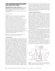
From the graphics of Fig. 14, it can be observed that<br />
good filter response <strong>for</strong> both the bands is obtained without<br />
interference between them. Reflection S 11 and isolation S 31<br />
parameters are below -14 dB, showing a good<br />
per<strong>for</strong>mance of the structure.<br />
Figure 13. Photograph of the two band multiplexing network.
References<br />
[1] Richard J. Cameron, Ming Yu, “Design of Manifold<br />
Coupled <strong>Multi</strong>plexers”, IEEE Microwave Magazine,<br />
October 2007.<br />
[2] G. Matthaei, L. Young, E.M.T. Jones, Microwave <strong>Filters</strong>,<br />
Impedance-Matching Networks, and Coupling Structures,<br />
Artech House 1985.<br />
[3] S. B. Cohn, F. S. Coale, “<strong>Directional</strong> Channel-Separation<br />
<strong>Filters</strong>”, Proceeding of the IRE, August, 1956.<br />
(a)<br />
[4] R. D. Wanselow, L. P. Tuttle Jr., “Practical Design of<br />
Strip-Transmission-Line Half-Wavelength Resonator<br />
<strong>Directional</strong> <strong>Filters</strong>”, IRE Transactions on Microwave<br />
Theory and Techniques, January, 1959.<br />
[5] H. Lobato-Morales, A. Corona-Chavez, J. Rodriguez-<br />
Asomoza, “Microwave <strong>Directional</strong> <strong>Filters</strong> using<br />
Metamaterial Closed-Loop Resonators”, Microwave and<br />
Optical Technology Letters, Vol. 51, No. 5, May 2009.<br />
[6] H. Lobato-Morales, A. Corona-Chávez, J. Rodríguez-<br />
Asomoza, “Novel Channelization <strong>Multi</strong>plexer using<br />
Metamaterial <strong>Filters</strong>”, IEEE Wireless and Microwave<br />
Technolgy Conference, WAMICON, 2009.<br />
[7] Jia-Shen G. Hong, M. J. Lancaster, <strong>Microstrip</strong> <strong>Filters</strong> <strong>for</strong><br />
RF/Microwave Applications, John Wiley and Sons, 2001.<br />
(b)<br />
Figure 14. Experimental multiplexer responses,<br />
(a) S 21<br />
, S 41<br />
and S 51<br />
, (b) S 11<br />
and S 31<br />
.<br />
6. Conclusions<br />
[8] Akira Hashimoto, Hitoshi Yoshino, and Hiroyuki Atarashi,<br />
“Roadmap of IMT-Advanced Development”, IEEE<br />
Microwave Magazine, Vol. 9, Issue 4, August 2008.<br />
[9] Rogerscorp, High frequency laminates, datasheet.<br />
[10] Sonnet EM Simulator ®, v. 11.54.<br />
<strong>Microstrip</strong> multi-<strong>pole</strong> directional filters are<br />
successfully proposed, analyzed and designed based on<br />
narrow stopband filter theory. Two microstrip directional<br />
filters <strong>for</strong> wireless applications are designed and tested. A<br />
two-band multiplexing network is implemented based on<br />
the proposed directional filters showing a good frequency<br />
per<strong>for</strong>mance, and maintaining the multi-<strong>pole</strong> response <strong>for</strong><br />
each proposed band.<br />
The directional filter scalable modular concept is<br />
demonstrated <strong>for</strong> multiplexing applications, adding the<br />
novel and particular characteristic of a multi-<strong>pole</strong><br />
response <strong>for</strong> each band. These characteristics make this<br />
type of filters ideal candidates <strong>for</strong> multiplexing networks<br />
at microwave frequencies, compared with other<br />
technologies.