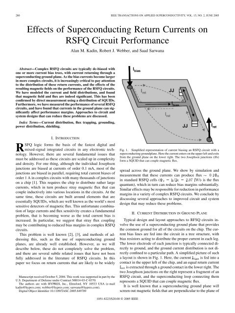
Effects of Superconducting Return Currents on RSFQ ... - IEEE Xplore
Effects of Superconducting Return Currents on RSFQ ... - IEEE Xplore
Effects of Superconducting Return Currents on RSFQ ... - IEEE Xplore

You also want an ePaper? Increase the reach of your titles
YUMPU automatically turns print PDFs into web optimized ePapers that Google loves.
280 <strong>IEEE</strong> TRANSACTIONS ON APPLIED SUPERCONDUCTIVITY, VOL. 15, NO. 2, JUNE 2005<br />
<str<strong>on</strong>g>Effects</str<strong>on</strong>g> <str<strong>on</strong>g>of</str<strong>on</strong>g> <str<strong>on</strong>g>Superc<strong>on</strong>ducting</str<strong>on</strong>g> <str<strong>on</strong>g>Return</str<strong>on</strong>g> <str<strong>on</strong>g>Currents</str<strong>on</strong>g> <strong>on</strong><br />
<strong>RSFQ</strong> Circuit Performance<br />
Alan M. Kadin, Robert J. Webber, and Saad Sarwana<br />
Abstract—Complex <strong>RSFQ</strong> circuits are typically dc-biased with<br />
<strong>on</strong>e or more current bias trees, with current returning through a<br />
superc<strong>on</strong>ducting ground plane. As the bias currents become larger<br />
in more complex circuits, it is increasingly critical to pay attenti<strong>on</strong><br />
to the distributi<strong>on</strong> <str<strong>on</strong>g>of</str<strong>on</strong>g> these return currents, and the effects <str<strong>on</strong>g>of</str<strong>on</strong>g> the<br />
resulting magnetic fields <strong>on</strong> the performance <str<strong>on</strong>g>of</str<strong>on</strong>g> the <strong>RSFQ</strong> circuits.<br />
We have modeled the current and field distributi<strong>on</strong>s, and found<br />
that magnetic field and flux are indeed significant. This has been<br />
c<strong>on</strong>firmed by direct measurement using a distributi<strong>on</strong> <str<strong>on</strong>g>of</str<strong>on</strong>g> SQUIDs.<br />
Furthermore, we have measured the performance <str<strong>on</strong>g>of</str<strong>on</strong>g> several <strong>RSFQ</strong><br />
circuits, and have found that currents in the ground plane can significantly<br />
affect performance margins. Approaches to circuit and<br />
system designs that can reduce these problems are discussed.<br />
Index Terms—Current distributi<strong>on</strong>, flux trapping, grounding,<br />
power distributi<strong>on</strong>, shielding.<br />
I. INTRODUCTION<br />
<strong>RSFQ</strong> logic forms the basis <str<strong>on</strong>g>of</str<strong>on</strong>g> the fastest digital and<br />
mixed-signal integrated circuits in any electr<strong>on</strong>ic technology.<br />
However, there are several fundamental issues that<br />
must be addressed as these circuits are scaled up in complexity<br />
and density. For <strong>on</strong>e thing, although the individual Josephs<strong>on</strong><br />
juncti<strong>on</strong>s are biased at currents <str<strong>on</strong>g>of</str<strong>on</strong>g> order 0.1 mA, most <str<strong>on</strong>g>of</str<strong>on</strong>g> the<br />
juncti<strong>on</strong>s are biased in parallel, requiring total current biases <str<strong>on</strong>g>of</str<strong>on</strong>g><br />
order 1 A in complex circuits with many thousands <str<strong>on</strong>g>of</str<strong>on</strong>g> juncti<strong>on</strong>s<br />
<strong>on</strong> a chip [1]. This requires the chip to distribute rather large<br />
currents, which in turn produce stray magnetic flux that can<br />
couple inductively into various locati<strong>on</strong>s in the circuits. At the<br />
same time, these circuits are built around elements that are<br />
essentially SQUIDs, which are well known as the world’s most<br />
sensitive detectors <str<strong>on</strong>g>of</str<strong>on</strong>g> magnetic flux. This unfortunate combinati<strong>on</strong><br />
<str<strong>on</strong>g>of</str<strong>on</strong>g> large currents and flux sensitivity creates a fundamental<br />
problem, that is becoming worse as the total current bias is<br />
increased. In particular, we suggest that stray flux coupling<br />
may be c<strong>on</strong>tributing to reduced bias margins in complex <strong>RSFQ</strong><br />
circuits.<br />
This problem is well known [2], [3], and methods <str<strong>on</strong>g>of</str<strong>on</strong>g> addressing<br />
this, such as the use <str<strong>on</strong>g>of</str<strong>on</strong>g> superc<strong>on</strong>ducting ground<br />
planes, are already well established. However, as we will<br />
describe below, these do not completely solve the problem,<br />
and there are several subtle related issues that have not been<br />
fully addressed in the literature <str<strong>on</strong>g>of</str<strong>on</strong>g> <strong>RSFQ</strong> circuits. In this<br />
paper we focus <strong>on</strong> return currents that are likely to be widely<br />
Manuscript received October 5, 2004. This work was supported in part by the<br />
U.S. Department <str<strong>on</strong>g>of</str<strong>on</strong>g> Defense undre C<strong>on</strong>tract N0014-03-C-0370.<br />
The authors are with HYPRES, Inc., Elmsford, NY 10533 USA (e-mail<br />
kadin@hypres.com; webber@hypres.com; sarwana@hypres.com).<br />
Digital Object Identifier 10.1109/TASC.2005.849789<br />
Fig. 1. Simplified representati<strong>on</strong> <str<strong>on</strong>g>of</str<strong>on</strong>g> current biasing an <strong>RSFQ</strong> circuit with a<br />
superc<strong>on</strong>ducting groundplane. Here the current enters <strong>on</strong> the upper left and exits<br />
from the ground plane <strong>on</strong> the lower right. The two Josephs<strong>on</strong> juncti<strong>on</strong>s (JJs)<br />
form a SQUID that can couple magnetic flux.<br />
spread across the ground plane. We show by simulati<strong>on</strong> and<br />
measurement that these currents can produce flux<br />
in standard <strong>RSFQ</strong> cells (<br />
is the flux<br />
quantum), which in turn can reduce bias margins substantially.<br />
Similar effects may be resp<strong>on</strong>sible for reducti<strong>on</strong> in performance<br />
margins in a variety <str<strong>on</strong>g>of</str<strong>on</strong>g> complex <strong>RSFQ</strong> circuits. We c<strong>on</strong>clude by<br />
discussing several approaches to improved circuit and system<br />
design that may reduce these problems.<br />
II. CURRENT DISTRIBUTION IN GROUND PLANE<br />
Typical design and layout approaches to RFSQ circuits involve<br />
the use <str<strong>on</strong>g>of</str<strong>on</strong>g> a superc<strong>on</strong>ducting ground plane that provides<br />
the comm<strong>on</strong> ground for all <str<strong>on</strong>g>of</str<strong>on</strong>g> the circuits <strong>on</strong> the chip. The current<br />
bias lines are fed into the circuit in a tree structure, with<br />
bias resistors acting to distribute the proper current in each leg.<br />
The lower electrode <str<strong>on</strong>g>of</str<strong>on</strong>g> each juncti<strong>on</strong> is typically c<strong>on</strong>nected directly<br />
to ground, and the ground current distributi<strong>on</strong> is not directly<br />
c<strong>on</strong>fined to a particular path. A simplified picture <str<strong>on</strong>g>of</str<strong>on</strong>g> such<br />
a layout is shown in Fig. 1. Here, the current is fed into a<br />
c<strong>on</strong>tact in the upper left <str<strong>on</strong>g>of</str<strong>on</strong>g> the chip, and an equal return current<br />
is extracted through a ground c<strong>on</strong>tact in the lower right. The<br />
two Josephs<strong>on</strong> juncti<strong>on</strong>s <strong>on</strong> the right represent a fragment <str<strong>on</strong>g>of</str<strong>on</strong>g> an<br />
<strong>RSFQ</strong> circuit, and the superc<strong>on</strong>ducting loop c<strong>on</strong>necting them<br />
represents a SQUID that can couple magnetic flux.<br />
It is well known that a superc<strong>on</strong>ducting ground plane will<br />
screen out magnetic fields that are perpendicular to the plane <str<strong>on</strong>g>of</str<strong>on</strong>g><br />
1051-8223/$20.00 © 2005 <strong>IEEE</strong>
KADIN et al.: EFFECTS OF SUPERCONDUCTING RETURN CURRENTS ON <strong>RSFQ</strong> CIRCUIT PERFORMANCE 281<br />
the film. It does this by inducing “image currents” that oppose<br />
the applied field, cancelling out the perpendicular comp<strong>on</strong>ent.<br />
This works well in screening out the field produced by a bias<br />
current that enters the chip in a line above the ground plane.<br />
As in standard microstrip at higher frequencies, a return current<br />
is induced directly underneath the strip, with a matching current.<br />
This c<strong>on</strong>fines the magnetic field between the strip and the<br />
ground plane, with fringe fields that decay from the edges as a<br />
dipole field, approximately as , where d is the separati<strong>on</strong><br />
<str<strong>on</strong>g>of</str<strong>on</strong>g> the line from the ground plane and r is the distance from the<br />
edge <str<strong>on</strong>g>of</str<strong>on</strong>g> the line. For a typical d , this edge field is<br />
completely negligible more than from the edge.<br />
But the situati<strong>on</strong> becomes more complicated near the input<br />
c<strong>on</strong>tact for the bias current. In particular, the return current<br />
that had been traveling underneath the input line now has to find<br />
its way to the ground c<strong>on</strong>tact, which in Fig. 1 is <strong>on</strong> the opposite<br />
corner <str<strong>on</strong>g>of</str<strong>on</strong>g> the chip. In doing so, it is no l<strong>on</strong>ger narrowly c<strong>on</strong>fined,<br />
and can spread out across the chip. In effect, the ground<br />
plane beneath the current input c<strong>on</strong>tact becomes a virtual current<br />
source with a radial spread, coupled with a virtual current<br />
sink at the ground c<strong>on</strong>tact <strong>on</strong> the other side. These spreading<br />
and c<strong>on</strong>verging currents can also be viewed as image currents<br />
for the vertical inserti<strong>on</strong> and extracti<strong>on</strong> wires.<br />
It is also important to note that most <str<strong>on</strong>g>of</str<strong>on</strong>g> the unc<strong>on</strong>strained current<br />
in a superc<strong>on</strong>ducting film does not flow near the outer edge,<br />
c<strong>on</strong>trary to comm<strong>on</strong> belief. It is certainly true that the current<br />
density J peaks sharply near the edge (<strong>on</strong> the scale <str<strong>on</strong>g>of</str<strong>on</strong>g> the magnetic<br />
penetrati<strong>on</strong> depth ), but if <strong>on</strong>e integrates J across a wide<br />
film, most <str<strong>on</strong>g>of</str<strong>on</strong>g> the total current I flows straight across the interior<br />
<str<strong>on</strong>g>of</str<strong>on</strong>g> the film. Since we are most c<strong>on</strong>cerned about the magnetic<br />
field in the interior (since that is where the <strong>RSFQ</strong> circuits are<br />
located), we can estimate the surface current density to a first<br />
approximati<strong>on</strong> by , where r is the radial distance and<br />
the appropriate spreading angle. The magnetic field H produced<br />
by this spreading current is equal to the surface current density<br />
J, but perpendicular, pointing in the azimuthal rather than the<br />
radial directi<strong>on</strong>. There is, <str<strong>on</strong>g>of</str<strong>on</strong>g> course, no vertical comp<strong>on</strong>ent <str<strong>on</strong>g>of</str<strong>on</strong>g><br />
field.<br />
The key point <str<strong>on</strong>g>of</str<strong>on</strong>g> this crude estimate is that the magnetic fields<br />
and fluxes induced by these spreading currents can be quite<br />
large. For example, if <strong>on</strong>e c<strong>on</strong>siders a 100 mA ground return<br />
current crossing a 0.5 cm chip, the surface current density in the<br />
middle <str<strong>on</strong>g>of</str<strong>on</strong>g> the chip would be .<br />
This produces and . This is<br />
about half the earth’s magnetic field (50 ). Given the great<br />
pains that are taken to screen out the earth’s field in <strong>RSFQ</strong> cryoprobes,<br />
it is clear that a field <str<strong>on</strong>g>of</str<strong>on</strong>g> this magnitude is unacceptable.<br />
This is also evident for a typical area <str<strong>on</strong>g>of</str<strong>on</strong>g> flux coupling, say for<br />
two juncti<strong>on</strong>s 20 apart, with an effective interlayer height<br />
<str<strong>on</strong>g>of</str<strong>on</strong>g> 0.5 . If this area is oriented to couple the maximum flux,<br />
25 gives a flux . Although the<br />
details would depend <strong>on</strong> the specific circuit, a flux change in a<br />
critical loop <str<strong>on</strong>g>of</str<strong>on</strong>g> order 10% <str<strong>on</strong>g>of</str<strong>on</strong>g> would be expected to affect bias<br />
currents <str<strong>on</strong>g>of</str<strong>on</strong>g> an <strong>RSFQ</strong> circuit by a similar factor. This is comparable<br />
to critical margins in complex circuits, and might prevent<br />
proper functi<strong>on</strong>ing <str<strong>on</strong>g>of</str<strong>on</strong>g> some circuits.<br />
Of course, the c<strong>on</strong>figurati<strong>on</strong> in Fig. 1 is rather oversimplified.<br />
In a more typical <strong>RSFQ</strong> chip, there are multiple current bias<br />
Fig. 2. Schematic <str<strong>on</strong>g>of</str<strong>on</strong>g> typical biasing scheme for <strong>RSFQ</strong> circuit, with a ground<br />
plane and a comm<strong>on</strong> ground for all bias lines. Current is injected into the<br />
circuit via multiple grounded bias sources. The return current is extracted<br />
through multiple ground c<strong>on</strong>tracts that are distributed around the periphery <str<strong>on</strong>g>of</str<strong>on</strong>g><br />
the chip. The distributi<strong>on</strong> <str<strong>on</strong>g>of</str<strong>on</strong>g> this extracti<strong>on</strong> currents am<strong>on</strong>g the ground c<strong>on</strong>tacts<br />
is determined by parasitic resistances to a comm<strong>on</strong> <str<strong>on</strong>g>of</str<strong>on</strong>g>f-chip ground. The spatial<br />
mismatches between local current sources and sinks can lead to significant<br />
cross-chip currents that may be <str<strong>on</strong>g>of</str<strong>on</strong>g> order 100 mA or more.<br />
inputs and multiple ground c<strong>on</strong>tacts around the chip. A somewhat<br />
more realistic model is indicated in Fig. 2. Now there are<br />
two bias sources, with a comm<strong>on</strong> ground, and 8 ground c<strong>on</strong>tacts<br />
around the chip. The return currents extracted through each<br />
ground c<strong>on</strong>tact are not specifically c<strong>on</strong>strained; <strong>on</strong>ly the total<br />
ground current is c<strong>on</strong>strained to match the total bias current. The<br />
distributi<strong>on</strong> <str<strong>on</strong>g>of</str<strong>on</strong>g> the return current am<strong>on</strong>g the ground c<strong>on</strong>tacts is<br />
determined by small, largely parasitic resistances to the <str<strong>on</strong>g>of</str<strong>on</strong>g>f-chip<br />
ground. (The superc<strong>on</strong>ducting inductances are important <strong>on</strong>ly in<br />
determining distributi<strong>on</strong>s <strong>on</strong> the ground plane itself.) For similar<br />
resistances, this return current extracti<strong>on</strong> may be approximately<br />
symmetrical around the chip. On the other hand, the bias currents<br />
are typically not symmetrical around the chip. This mismatch<br />
creates excess bias currents crossing the ground plane,<br />
coupling flux into <strong>RSFQ</strong> circuit elements and reducing bias margins.<br />
Since the total bias current in a complex <strong>RSFQ</strong> circuits can<br />
approach 1 A, significant mismatches requiring cross-chip currents<br />
<str<strong>on</strong>g>of</str<strong>on</strong>g> order 100 mA are quite likely. As discussed earlier, this<br />
can lead to flux coupling in some <str<strong>on</strong>g>of</str<strong>on</strong>g> the internal SQUID loops<br />
in <strong>RSFQ</strong> circuits, and c<strong>on</strong>sequent narrowing <str<strong>on</strong>g>of</str<strong>on</strong>g> critical margins.<br />
To provide further evidence <str<strong>on</strong>g>of</str<strong>on</strong>g> these ground-current distributi<strong>on</strong>s,<br />
we tested a particular 0.5-cm diagnostic chip<br />
(ak6_diag0ch03) fabricated using the HYPRES standard<br />
process [4] for 1<br />
juncti<strong>on</strong>s (Fig. 3). This chip<br />
includes a number <str<strong>on</strong>g>of</str<strong>on</strong>g> independently biased SQUIDs, with<br />
geometries similar to those in standard <strong>RSFQ</strong> cells. Each <str<strong>on</strong>g>of</str<strong>on</strong>g><br />
these SQUIDs permits direct injecti<strong>on</strong> <str<strong>on</strong>g>of</str<strong>on</strong>g> current into<br />
the upper line <str<strong>on</strong>g>of</str<strong>on</strong>g> the SQUID, in order to calibrate the line<br />
inductance. In additi<strong>on</strong>, this chip permits <strong>on</strong>e to inject current<br />
directly into the ground plane in the corner. The measured<br />
results at 4.2 K for <strong>on</strong>e particular SQUID are summarized in<br />
Fig. 3, for a fixed bias current placing the SQUID in the voltage<br />
state for . Here the transfer characteristic <str<strong>on</strong>g>of</str<strong>on</strong>g> the
282 <strong>IEEE</strong> TRANSACTIONS ON APPLIED SUPERCONDUCTIVITY, VOL. 15, NO. 2, JUNE 2005<br />
Fig. 3. Nb chip (5 mm 2 5 mm) to dem<strong>on</strong>strate distributi<strong>on</strong> <str<strong>on</strong>g>of</str<strong>on</strong>g> currents in<br />
superc<strong>on</strong>ducting ground plane. Top: chip layout showing array <str<strong>on</strong>g>of</str<strong>on</strong>g> SQUIDs<br />
around chip, focusing <strong>on</strong> a particular SQUID, with simplified circuit schematic<br />
also shown. Bottom: measured shift <str<strong>on</strong>g>of</str<strong>on</strong>g> V 0 8 transfer characteristic <str<strong>on</strong>g>of</str<strong>on</strong>g> SQUID<br />
with injected current I . The slope <str<strong>on</strong>g>of</str<strong>on</strong>g> this line corresp<strong>on</strong>ds to a mutual<br />
inductance M=1:8 fH.<br />
SQUID shifts proporti<strong>on</strong>ally to the separate current (<str<strong>on</strong>g>of</str<strong>on</strong>g> either<br />
sign) injected into the ground plane in the lower left corner.<br />
The slope <str<strong>on</strong>g>of</str<strong>on</strong>g> this curve corresp<strong>on</strong>ds to a mutual inductance<br />
. This seems like a rather small coupling, but it<br />
does in fact corresp<strong>on</strong>d to flux shifts <str<strong>on</strong>g>of</str<strong>on</strong>g> 10% <str<strong>on</strong>g>of</str<strong>on</strong>g> for currents<br />
<str<strong>on</strong>g>of</str<strong>on</strong>g> order 100 mA, as we suggested earlier.<br />
One can compare the measured value<br />
to a very<br />
simple model <str<strong>on</strong>g>of</str<strong>on</strong>g> radial spreading current, with ,<br />
where A is the SQUID area, the spreading angle, and r the radial<br />
distance. Taking , , and<br />
, yields . A more realistic calculati<strong>on</strong> would<br />
take into account partial extracti<strong>on</strong> <str<strong>on</strong>g>of</str<strong>on</strong>g> ground current (about<br />
half) through ground pads (the inner ring <str<strong>on</strong>g>of</str<strong>on</strong>g> 36 ground c<strong>on</strong>tacts)<br />
before the current reaches the SQUID, and also the misaligned<br />
flux coupling angle, both <str<strong>on</strong>g>of</str<strong>on</strong>g> which would reduce the effective<br />
coupling toward the measured value. Preliminary simulati<strong>on</strong>s<br />
with a two-dimensi<strong>on</strong>al finite-element program are c<strong>on</strong>sistent<br />
with this expectati<strong>on</strong>.<br />
III. TEST OF <strong>RSFQ</strong> OPERATING MARGINS<br />
Finally, a direct test <str<strong>on</strong>g>of</str<strong>on</strong>g> <strong>RSFQ</strong> operating margins was made,<br />
using a 5-mm chip (ak6019ch02) c<strong>on</strong>taining two separate<br />
<strong>RSFQ</strong> circuits: a 4-bit parallel adder, and a D-Flip-Flop<br />
(Fig. 4). The <strong>on</strong>ly c<strong>on</strong>necti<strong>on</strong> between the two circuits is<br />
through the ground plane. The bias current for the adder was<br />
much larger ( 100 mA) than that for the DFF ( 10 mA), so<br />
the bias margins <str<strong>on</strong>g>of</str<strong>on</strong>g> the DFF were tested for varying currents<br />
into the adder. Since operati<strong>on</strong> <str<strong>on</strong>g>of</str<strong>on</strong>g> the adder was not checked,<br />
this “Main Adjustable Bias” (MAB) essentially provided a way<br />
to inject current in the ground plane. Automated low-speed operati<strong>on</strong><br />
<str<strong>on</strong>g>of</str<strong>on</strong>g> the DFF was carried out at 4.2 K using the “Octopux”<br />
Fig. 4. Margins test <str<strong>on</strong>g>of</str<strong>on</strong>g> D-flip-flop (DFF). The top shows the layout <str<strong>on</strong>g>of</str<strong>on</strong>g> the<br />
chip, with a larger 4-bit parallel adder (center) and also a DFF (upper right).<br />
The bottom shows the measured values <str<strong>on</strong>g>of</str<strong>on</strong>g> DFF current bias (in mA) for proper<br />
(low-speed) operati<strong>on</strong> <str<strong>on</strong>g>of</str<strong>on</strong>g> the circuit, for various values <str<strong>on</strong>g>of</str<strong>on</strong>g> the “main adjustable<br />
bias” (MAB) <str<strong>on</strong>g>of</str<strong>on</strong>g> the adder, <str<strong>on</strong>g>of</str<strong>on</strong>g> either sign. Note that for positive MAB bias, the<br />
operating margins <str<strong>on</strong>g>of</str<strong>on</strong>g> the DFF actually increased, while the margins shrank for<br />
negative bias.<br />
programmable test system. A two-dimensi<strong>on</strong>al M<strong>on</strong>te-Carlo set<br />
<str<strong>on</strong>g>of</str<strong>on</strong>g> current parameters were chosen, with both the MAB and the<br />
DFF bias varied across relevant ranges, including both signs <str<strong>on</strong>g>of</str<strong>on</strong>g><br />
MAB current. The points corresp<strong>on</strong>ding to proper operati<strong>on</strong> <str<strong>on</strong>g>of</str<strong>on</strong>g><br />
the DFF are shown in Fig. 4, indicating the operating margins<br />
<str<strong>on</strong>g>of</str<strong>on</strong>g> the circuit. It is clear that this margins plot is asymmetric,<br />
with positive MAB currents actually increasing the margins,<br />
at least for currents up to 50 mA. Negative currents, <strong>on</strong> the<br />
other hand, sharply decrease the operating margins.<br />
One can understand this asymmetry by noting that the<br />
positive self-bias <str<strong>on</strong>g>of</str<strong>on</strong>g> the DFF, 10 mA (including for the<br />
input and output circuits), would also be expected to produce<br />
spreading current in the ground plane near the circuit. We can<br />
crudely estimate that this current is spread across a distance<br />
2 mm near the DFF, corresp<strong>on</strong>ding to a surface current<br />
density . For a typical 10<br />
coupling area, this corresp<strong>on</strong>ds to a flux 3% <str<strong>on</strong>g>of</str<strong>on</strong>g> . For a<br />
circuit designed without taking this into account, <strong>on</strong>e would<br />
expect a small but significant narrowing <str<strong>on</strong>g>of</str<strong>on</strong>g> operating margins,<br />
as is indeed observed. For a positive MAB current, however,<br />
the expected ground return currents, in the regi<strong>on</strong> near the<br />
DFF, would be expected to point in the opposite directi<strong>on</strong>.<br />
In particular, if we c<strong>on</strong>sider a MAB current <str<strong>on</strong>g>of</str<strong>on</strong>g> 50 mA, and<br />
estimate that 20 mA remains uncollected when it is spread<br />
over 4 mm near the DFF, this also corresp<strong>on</strong>ds to .
KADIN et al.: EFFECTS OF SUPERCONDUCTING RETURN CURRENTS ON <strong>RSFQ</strong> CIRCUIT PERFORMANCE 283<br />
To the extent that this is properly oriented to oppose the current<br />
produced by the DFF bias, the net flux coupled would cancel<br />
out, and the operating margins would recover toward their ideal<br />
range. This, too, is observed. A further increase in MAB bias<br />
would then start to reverse the sign <str<strong>on</strong>g>of</str<strong>on</strong>g> the coupled flux, leading<br />
to a decrease in margin. Such a turnaround also seems to be<br />
present in the data <str<strong>on</strong>g>of</str<strong>on</strong>g> Fig. 4. For negative MAB currents, the<br />
flux will reinforce the self-flux that is already present, further<br />
reducing the margin. For example, for MAB current <str<strong>on</strong>g>of</str<strong>on</strong>g> 100<br />
mA, we estimate that the surface current density near the DFF<br />
is<br />
, which corresp<strong>on</strong>ds to a<br />
flux <str<strong>on</strong>g>of</str<strong>on</strong>g> . The data show a margin that is reduced<br />
from about 75% to about 50%.<br />
This all presents a c<strong>on</strong>sistent picture, but agreement is semiquantitative<br />
at best. We d<strong>on</strong>’t even really know which is the critical<br />
SQUID loop in the circuit resp<strong>on</strong>sible for these margins. A<br />
more accurate analysis would need to take into account detailed<br />
current distributi<strong>on</strong>s in the ground plane, flux coupling geometries,<br />
and models <str<strong>on</strong>g>of</str<strong>on</strong>g> the flux sensitivities <str<strong>on</strong>g>of</str<strong>on</strong>g> the various elemental<br />
cells <str<strong>on</strong>g>of</str<strong>on</strong>g> <strong>RSFQ</strong> circuits.<br />
IV. DISCUSSION AND CONCLUSIONS<br />
All <str<strong>on</strong>g>of</str<strong>on</strong>g> this provides str<strong>on</strong>g evidence that these are important<br />
effects that must be taken into account for optimum performance<br />
<str<strong>on</strong>g>of</str<strong>on</strong>g> complex <strong>RSFQ</strong> circuits. It is worth emphasizing<br />
that these measurements were carried out inside two c<strong>on</strong>centric<br />
mu-metal cans, in order to screen out the earth’s magnetic field<br />
( or 50 ), and we believe that they were very effective<br />
at doing so. However, the local fields at the <strong>RSFQ</strong> circuits,<br />
produced by ground return currents, are almost as big, and are<br />
not effectively screened.<br />
So other strategies must be employed to reduce these effects.<br />
These include balancing the locati<strong>on</strong>s <str<strong>on</strong>g>of</str<strong>on</strong>g> current biases and<br />
ground c<strong>on</strong>tacts around the chip, so that there is no need for<br />
large cross-chip currents and fields. One could also design a<br />
cryoprobe with separate dedicated return lines for each large<br />
bias current. If such a return line is c<strong>on</strong>nected to a ground<br />
c<strong>on</strong>tract right next to the corresp<strong>on</strong>ding bias c<strong>on</strong>tact <strong>on</strong> the<br />
chip, that would also reduce the need for such unbalanced<br />
currents. Of course, this approach requires that the return<br />
current be c<strong>on</strong>strained closely to match the given bias current,<br />
which requires either transformer-isolated power supplies, or<br />
alternatively matched source-and-sink module pairs. One can<br />
also remove the ground plane where it is not directly needed<br />
(such as under bias lines, inductors, and transmissi<strong>on</strong> lines).<br />
This will tend to c<strong>on</strong>strain the current flow away from the<br />
critical regi<strong>on</strong>s, although if <strong>on</strong>e is not careful, this may simply<br />
make the problem worse elsewhere <strong>on</strong> the chip. Another important<br />
design strategy is to make use <str<strong>on</strong>g>of</str<strong>on</strong>g> “current recycling”<br />
[5], whereby repetitive circuit blocks are biased in series, thus<br />
reducing the total bias current to the chip.<br />
Another important approach, which we have adapted in many<br />
<str<strong>on</strong>g>of</str<strong>on</strong>g> our <strong>RSFQ</strong> circuits, is the use <str<strong>on</strong>g>of</str<strong>on</strong>g> a double ground plane. In this<br />
approach, there is a top superc<strong>on</strong>ducting layer above the circuit<br />
elements, which is grounded to the lower layer with frequent superc<strong>on</strong>ducting<br />
vias. This creates a large number <str<strong>on</strong>g>of</str<strong>on</strong>g> flat superc<strong>on</strong>ducting<br />
loops around the SQUID loops. If the flux in any loop is<br />
initially zero, then it will remain zero. Therefore, any extended<br />
ground current will be split between the upper and lower ground<br />
planes, which should sharply reduce the flux coupled in a given<br />
SQUID loop. We have not yet carried out a systematic comparis<strong>on</strong><br />
<str<strong>on</strong>g>of</str<strong>on</strong>g> margin effects with and without the upper ground plane,<br />
but the preliminary evidence suggests that the ground-current<br />
effect is significantly reduced (but not eliminated). On the other<br />
hand, superc<strong>on</strong>ducting loops near critical circuit elements may<br />
also increase the likelihood <str<strong>on</strong>g>of</str<strong>on</strong>g> flux trapping, if <strong>on</strong>e is not careful.<br />
In c<strong>on</strong>clusi<strong>on</strong>, we have identified a serious problem with<br />
ground return currents in <strong>RSFQ</strong> circuits with total bias approaching<br />
1 A, namely that magnetic flux coupled into internal<br />
SQUID loops can degrade circuit performance. This problem<br />
can be significantly reduced by a combinati<strong>on</strong> <str<strong>on</strong>g>of</str<strong>on</strong>g> strategies<br />
<strong>on</strong> the design, layout, and system levels. If these are properly<br />
implemented, further increases in integrati<strong>on</strong> scale <str<strong>on</strong>g>of</str<strong>on</strong>g> <strong>RSFQ</strong><br />
circuits can c<strong>on</strong>tinue to be achieved.<br />
REFERENCES<br />
[1] O. A. Mukhanov, D. Gupta, A. M. Kadin, and V. K. Semenov, “Superc<strong>on</strong>ductive<br />
analog-to-digital c<strong>on</strong>verters,” Proc. <strong>IEEE</strong>, vol. 92, pp.<br />
1564–1584, Oct. 2004.<br />
[2] H. Terai, Y. Kameda, S. Yorozu, A. Fujimaki, and Z. Weng, “The effects<br />
<str<strong>on</strong>g>of</str<strong>on</strong>g> dc bias current in large-scale SFQ circuits,” <strong>IEEE</strong> Trans. Appl. Superc<strong>on</strong>d.,<br />
vol. 13, no. 2, pp. 502–506, Jun. 2003.<br />
[3] M. Suzuki, M. Maezawa, and F. Hirayama, “<str<strong>on</strong>g>Effects</str<strong>on</strong>g> <str<strong>on</strong>g>of</str<strong>on</strong>g> magnetic fields<br />
induced by bias currents <strong>on</strong> operati<strong>on</strong> <str<strong>on</strong>g>of</str<strong>on</strong>g> <strong>RSFQ</strong> circuits,” Physica C, vol.<br />
412, pp. 1576–1579, Oct. 2004.<br />
[4] M. Radparvar, “<str<strong>on</strong>g>Superc<strong>on</strong>ducting</str<strong>on</strong>g> Nb and NbN processes for mediumscale<br />
integrati<strong>on</strong> processes,” Cryogenics, vol. 35, pp. 535–540, 1995.<br />
See also http://www.hypres.com/pages/download/designrules/rules.pdf.<br />
[5] J. H. Kang and S. B. Kaplan, “Current recycling and SFQ current transfer<br />
in large-scale <strong>RSFQ</strong> circuits,” <strong>IEEE</strong> Trans. Appl. Superc<strong>on</strong>d., vol. 13, no.<br />
2, pp. 547–550, Jun. 2003.