Transistors to Transformations - Intel
Transistors to Transformations - Intel
Transistors to Transformations - Intel

Create successful ePaper yourself
Turn your PDF publications into a flip-book with our unique Google optimized e-Paper software.
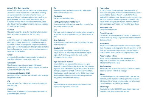
22nm 3-D Tri-Gate transis<strong>to</strong>r<br />
<strong>Intel</strong>’s 3-D Tri-Gate transis<strong>to</strong>r uses three gates wrapped<br />
around the silicon channel in a 3-D structure, enabling<br />
an unprecedented combination of performance and<br />
energy efficiency. <strong>Intel</strong> designed the new transis<strong>to</strong>r <strong>to</strong><br />
provide unique, ultra-low power benefits for use in<br />
handheld devices, like smartphones and tablets, while<br />
also delivering improved performance normally expected<br />
for high-end processors.<br />
Channel<br />
The region under the gate of a transis<strong>to</strong>r where current<br />
flows when the transis<strong>to</strong>r is in the “on” state.<br />
Chip<br />
A tiny, thin square or rectangle that contains integrated<br />
electronic circuitry. Die are built in batches on wafers<br />
of silicon. A chip is a packaged die. Chips are also called<br />
processors and microprocessors. Microprocessors are the<br />
brains of computers, servers, communications products,<br />
and other digital devices.<br />
Circuit<br />
A network of transis<strong>to</strong>rs interconnected by wires in a<br />
specific configuration <strong>to</strong> perform a function.<br />
Cleanroom<br />
The ultra-clean room where chips are fabricated.<br />
Cleanroom air is thousands of times cleaner than that in a<br />
typical hospital operating room.<br />
Computer-aided design (CAD)<br />
Computerized workstations and software used <strong>to</strong> design<br />
integrated circuits.<br />
Die<br />
Alternate name for a chip, usually before it is packaged.<br />
See also Chip.<br />
Etching<br />
The removal of selected portions of materials <strong>to</strong> define<br />
patterned layers on chips.<br />
Fab<br />
A shortened term for fabrication facility, where <strong>Intel</strong><br />
manufactures silicon chips.<br />
Fabrication<br />
The process of making chips.<br />
Front-opening unified pod (FOUP)<br />
A container that holds and carries wafers as part of an<br />
au<strong>to</strong>mated system in a fab.<br />
Gate<br />
The input control region of a transis<strong>to</strong>r where a negative<br />
or positive charge is applied <strong>to</strong> block or allow current <strong>to</strong><br />
flow.<br />
Gate dielectric<br />
A thin layer underneath the gate that isolates the gate<br />
from the channel.<br />
Gigabyte (GB)<br />
One gigabyte is one billion (1,000,000,000) bytes.<br />
A byte is a unit of computing information that equals<br />
eight bits. A bit (binary digit) is the basic unit of<br />
information in computing.<br />
High-k dielectric material<br />
A material that can replace silicon dioxide as a gate<br />
dielectric. It has good insulating properties and creates a<br />
high field effect between the gate and channel. Both are<br />
desirable properties for high-performance transis<strong>to</strong>rs.<br />
Also, because high-k materials can be thicker than silicon<br />
dioxide while retaining the same desirable properties,<br />
they greatly reduce current leakage.<br />
Mask<br />
A stencil-like pattern used during fabrication <strong>to</strong> print<br />
layered circuit patterns on a wafer.<br />
Moore’s law<br />
In 1965, Gordon Moore predicted that the number of<br />
transis<strong>to</strong>rs on a piece of silicon would double every year —<br />
an insight later dubbed Moore’s Law. In 1975, Moore<br />
updated his prediction that the number of transis<strong>to</strong>rs that<br />
the industry would be able <strong>to</strong> place on a computer chip<br />
would double every couple of years. As the number of<br />
transis<strong>to</strong>rs goes up, the cost per transis<strong>to</strong>r goes down.<br />
Nanometer (nm)<br />
One billionth of a meter.<br />
Pho<strong>to</strong>lithography<br />
The process of creating a specific pattern of material on<br />
a silicon wafer by using UV light and a mask <strong>to</strong> define the<br />
desired pattern.<br />
Pho<strong>to</strong>resist<br />
A substance that becomes soluble when exposed <strong>to</strong> UV<br />
light. Analogous <strong>to</strong> pho<strong>to</strong>graphic film, it is sensitive <strong>to</strong> UV<br />
light, but is also resistant <strong>to</strong> certain etching chemicals.<br />
Used <strong>to</strong> define circuit patterns during chip fabrication.<br />
Polycrystalline silicon<br />
Silicon made up of many crystals, also known as<br />
polysilicon. This conductive material is used as an<br />
interconnect layer on a chip.<br />
Semiconduc<strong>to</strong>r<br />
A material (such as silicon) that can be altered <strong>to</strong> conduct<br />
electrical current or block its passage.<br />
Silicon<br />
The principal ingredient in common beach sand and the<br />
element used <strong>to</strong> make the wafers upon which chips are<br />
fabricated. It is a natural semiconduc<strong>to</strong>r and is the most<br />
common element on Earth after oxygen.<br />
Silicon ingot<br />
A cylinder formed of 99.9999% pure silicon. Ingots are<br />
sliced in<strong>to</strong> thin silicon discs called wafers.