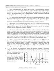
QAM and QPSK:
QAM and QPSK:
QAM and QPSK:

Create successful ePaper yourself
Turn your PDF publications into a flip-book with our unique Google optimized e-Paper software.
Not shown is the method of carrier acquisition. This ensures that the oscillator, which<br />
supplies the local carrier signal, is synchronized to the received (input) signal in both<br />
frequency <strong>and</strong> phase. In this experiment we will use a stole carrier to ensure that carrier<br />
signal in the transmitter <strong>and</strong> receiver are in synchronism with each other. (Please read<br />
about Costas Receiver to underst<strong>and</strong> more about carrier acquisition).<br />
In this experiment, two independent data sequences will be used at the input to the<br />
modulator, rather than having digital circuitry to split one data stream into two (the serialto-parallel<br />
converter). Two such independent data sequences, sharing a common bit clock<br />
(2.083 kHz), are available from a single SEQUENCE GENERATOR module. The data<br />
stream from which these two channels are considered to have been derived would have<br />
been at a rate of twice this - 4.167 kHz.<br />
Lowpass filter b<strong>and</strong>limiting <strong>and</strong> pulse shaping is not a subject of enquiry in this<br />
experiment. So a single b<strong>and</strong>pass filter at the ADDER (summer) output will suffice,<br />
providing it is of adequate b<strong>and</strong>width. A 100 kHz CHANNEL FILTERS module is<br />
acceptable (filter #3).<br />
Experimental Procedure:<br />
The <strong>QPSK</strong> transmitter:<br />
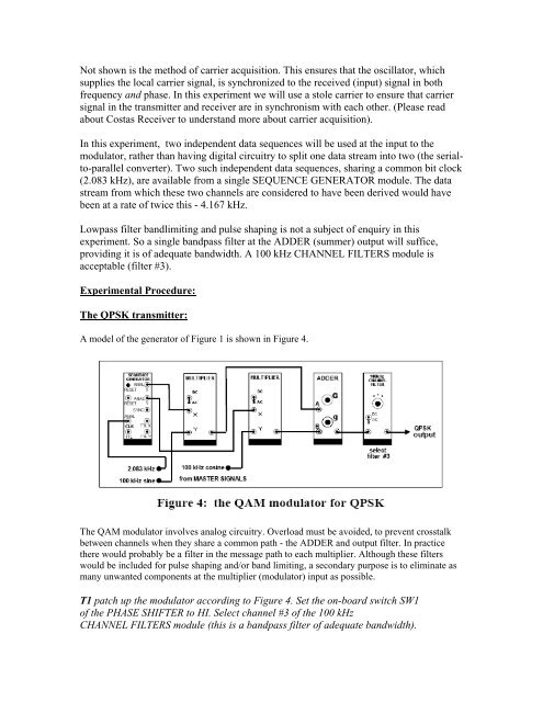
A model of the generator of Figure 1 is shown in Figure 4.<br />
The <strong>QAM</strong> modulator involves analog circuitry. Overload must be avoided, to prevent crosstalk<br />
between channels when they share a common path - the ADDER <strong>and</strong> output filter. In practice<br />
there would probably be a filter in the message path to each multiplier. Although these filters<br />
would be included for pulse shaping <strong>and</strong>/or b<strong>and</strong> limiting, a secondary purpose is to eliminate as<br />
many unwanted components at the multiplier (modulator) input as possible.<br />
T1 patch up the modulator according to Figure 4. Set the on-board switch SW1<br />
of the PHASE SHIFTER to HI. Select channel #3 of the 100 kHz<br />
CHANNEL FILTERS module (this is a b<strong>and</strong>pass filter of adequate b<strong>and</strong>width).