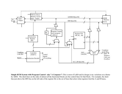
Simple RTM System with Program Control - aka "A Computer": This ...
Simple RTM System with Program Control - aka "A Computer": This ...
Simple RTM System with Program Control - aka "A Computer": This ...

Create successful ePaper yourself
Turn your PDF publications into a flip-book with our unique Google optimized e-Paper software.
The<br />
World<br />
Input -<br />
Output<br />
FSM for Direct<br />
Memory Access<br />
Input - Output<br />
ADDRESS[nn:00]<br />
DBUS[nn:00]<br />
ADDR<br />
Memory<br />
DATA<br />
Instruction<br />
Register<br />
(IR)<br />
+1<br />
<strong>Program</strong> Counter<br />
(next program<br />
address)<br />
Register File<br />
R0, R1,...Rn<br />
A<br />
DIN<br />
B<br />
Condition<br />
Code Bits<br />
BOOT<br />
<strong>Control</strong>ler<br />
(FSM??)<br />
Instruction Decoder<br />
<strong>Control</strong><br />
Signals<br />
to Everything<br />
ALU<br />
Function<br />
A B<br />
ALU<br />
Condition<br />
Code Bits:<br />
Zero<br />
Negative<br />
Carry out<br />
Overflow<br />
ALU_BUS[nn:00]<br />
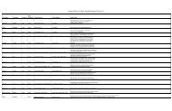
<strong>Simple</strong> <strong>RTM</strong> <strong>System</strong> <strong>with</strong> <strong>Program</strong> <strong>Control</strong> - <strong>aka</strong> "A Computer": <strong>This</strong> is most of LabD and its design is my variations on a theme<br />
by ARM. The short lines on the sides of almost all the functional blocks are the control lines for that block. For example, the short<br />
line just above the DIN bus on the left side of the register file is the set of lines that select what registers feed the A and B buses,
which register will be affected by a write operation and whether a write should take place. The control lines all originate in the<br />
Instruction Decoder. There are a number of ways to implement the controller block, some of which can use FSMs to produce<br />
sequences of control signals. The slash lines across many of the wires represent buses of whatever the standard data bus width is for<br />
that machine. In Lab D this is 16 bits. The use of tristate drivers for bus multiplexing is schematic of function rather than<br />
implementation. Some or all of that function may be done <strong>with</strong> multiplexers instead. The BOOT line at the lower left is asserted at<br />
turnon of power and forces the controller to fetch an instruction from a particular location in memory, often at address 0x00000.