TUTORIAL 2 1. Draw the energy band diagram of a conductor, an ...
TUTORIAL 2 1. Draw the energy band diagram of a conductor, an ...
TUTORIAL 2 1. Draw the energy band diagram of a conductor, an ...

Create successful ePaper yourself
Turn your PDF publications into a flip-book with our unique Google optimized e-Paper software.
<strong>TUTORIAL</strong> 2<br />
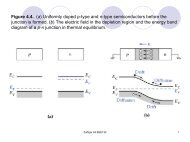
<strong>1.</strong> <strong>Draw</strong> <strong>the</strong> <strong>energy</strong> <strong>b<strong>an</strong>d</strong> <strong>diagram</strong> <strong>of</strong> a <strong>conductor</strong>, <strong>an</strong> insulator <strong>an</strong>d a semi<strong>conductor</strong>.<br />
Comment on <strong>the</strong> conductivity <strong>of</strong> <strong>the</strong> 3 materials with reference to <strong>the</strong> number <strong>of</strong> free<br />
electrons in <strong>the</strong> materials at room temperature.<br />
2. Discuss on <strong>the</strong> differences in <strong>the</strong> <strong>energy</strong> <strong>b<strong>an</strong>d</strong> structure <strong>of</strong> a <strong>conductor</strong>, <strong>an</strong> insulator <strong>an</strong>d a<br />
semi<strong>conductor</strong>.<br />
3. Name two examples <strong>of</strong> <strong>the</strong> elements that c<strong>an</strong> be used as donor <strong>an</strong>d acceptor impurities.<br />
Explain how <strong>the</strong> majority carriers are formed in <strong>the</strong> extrinsic semi<strong>conductor</strong>s.<br />
4. Define mobility <strong>an</strong>d conductivity. Calculate <strong>the</strong> conductivity <strong>of</strong> <strong>an</strong> intrinsic Silicon at<br />
room temperature (27°C). Given <strong>the</strong> intrinsic Silicon concentration n i = <strong>1.</strong>5x10 10 cm -3 , µ n<br />
= 1300 cm 2 /Vs, µ p = 500 cm 2 /Vs <strong>an</strong>d electronic charge, q = <strong>1.</strong>6x10 -19 C.<br />
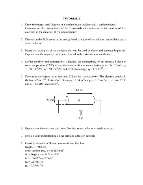
5. Determine <strong>the</strong> current in <strong>an</strong> extrinsic Silicon bar shown below. The electron density in<br />
<strong>the</strong> bar is 2.6x10 19 electron/m -3 . Given µ n = 0.14 m 2 /Vs, µ p = 0.05 m 2 /Vs, q = <strong>1.</strong>6x10 -19 C<br />
<strong>an</strong>d n i = <strong>1.</strong>4x10 16 electron/m 3 .<br />
<strong>1.</strong>4 cm<br />
20 mm<br />
Si<br />
12 V<br />
6. Explain how <strong>the</strong> electrons <strong>an</strong>d holes flow in a semi<strong>conductor</strong> crystal c<strong>an</strong> occur.<br />
7. Explain your underst<strong>an</strong>ding on <strong>the</strong> drift <strong>an</strong>d diffusion currents.<br />
8. Consider <strong>an</strong> intrinsic Silicon semi<strong>conductor</strong> that has:<br />
length, L = 0.8 cm<br />
cross-section area, s = 15x15 mm 2<br />
dc voltage across it, V = 10 V<br />
n i = <strong>1.</strong>5x10 16 electron/m 3<br />
µ n = 0.14 m 2 /Vs<br />
µ p = 0.05 m 2 /Vs
q = <strong>1.</strong>6x10 -19 C<br />
Calculate:<br />
(a) electron <strong>an</strong>d hole velocity<br />
(b) total current flowing through <strong>the</strong> semi<strong>conductor</strong><br />
9. A germ<strong>an</strong>ium sample is doped with 10 14 donor/cm 3 <strong>an</strong>d 7x10 13 acceptor/cm 3 . At room<br />
temperature, <strong>the</strong> pure Germ<strong>an</strong>ium resistivity is 60 Ωcm. If <strong>the</strong> electric field is 2 Vcm -1 ,<br />
determine <strong>the</strong> total current density. Assume that <strong>the</strong> electron <strong>an</strong>d hole mobility is 3900<br />
<strong>an</strong>d 1900 cm 2 V -1 s -1 , respectively.<br />
Note: Both donor <strong>an</strong>d acceptor impurities c<strong>an</strong> exist simult<strong>an</strong>eously. To preserve <strong>the</strong><br />
electrical neutrality, <strong>the</strong> positive charge density is equals to <strong>the</strong> negative charge density,<br />
i.e. p + N D = n + N A<br />
10. A Germ<strong>an</strong>ium bar has <strong>the</strong> following form:<br />
w<br />
h<br />
Given,<br />
L<br />
L = 1 cm<br />
h = w = 0.1 cm<br />
µ p = 2x10 3 cm 2 /Vs<br />
µ n = 4x10 3 cm 2 /Vs<br />
If <strong>the</strong> bar is intrinsic, n = p = n i = 2x10 13 cm -3 at 300°K. Determine conductivity, σ, <strong>an</strong>d<br />
resist<strong>an</strong>ce, R, measured across <strong>the</strong> bar.<br />
Note: The end <strong>of</strong> <strong>the</strong> bar has a surface area <strong>of</strong> wh <strong>an</strong>d R = L/ σwh.<br />
1<strong>1.</strong> The resist<strong>an</strong>ce <strong>of</strong> a semi<strong>conductor</strong> at room temperature was 5.5 MΩ. The resist<strong>an</strong>ce was<br />
reduced to 125 Ω when <strong>the</strong> material was doped with acceptor impurities. If <strong>the</strong>re were<br />
10 22 acceptor/m 3 <strong>of</strong> impurities <strong>an</strong>d <strong>the</strong> mobility <strong>of</strong> <strong>the</strong> electron is 2.8 times more th<strong>an</strong> <strong>the</strong>
mobility <strong>of</strong> holes, calculate <strong>the</strong> concentration <strong>of</strong> <strong>the</strong> electron-hole pair in <strong>the</strong> intrinsic<br />
specimen.<br />
12. The conductivity <strong>of</strong> <strong>an</strong> intrinsic Silicon crystal at room temperature was 5x10 -4 S/m. If<br />
<strong>the</strong> electron mobility was 0.14 m 2 /Vs <strong>an</strong>d <strong>the</strong> hole mobility was 0.05 m 2 /Vs, determine<br />
<strong>the</strong> concentration <strong>of</strong> <strong>the</strong> electron-hole pair in <strong>the</strong> crystal. If <strong>the</strong> crystal is doped with donor<br />
atoms to give <strong>an</strong> impurity concentration <strong>of</strong> 10 22 /m 3 , calculate <strong>the</strong> new value <strong>of</strong> <strong>the</strong><br />
conductivity <strong>an</strong>d <strong>the</strong> percentage <strong>of</strong> this conductivity that is contributed by <strong>the</strong> holes.<br />
Assume that all donor atoms are ionized <strong>an</strong>d <strong>the</strong> mobility <strong>of</strong> both electrons <strong>an</strong>d holes are<br />
maintained.<br />
13. Prove that <strong>the</strong> probability <strong>of</strong> <strong>an</strong> electron occupying <strong>an</strong> <strong>energy</strong> level E F + ΔE is equivalent<br />
to 1–f(E F + ΔE). E F is <strong>the</strong> Fermi level <strong>an</strong>d f(E) is <strong>the</strong> probability <strong>of</strong> <strong>an</strong> electron occupying<br />
<strong>an</strong> <strong>energy</strong> level E.<br />
14. An intrinsic semi<strong>conductor</strong> has <strong>an</strong> <strong>energy</strong> gap <strong>of</strong> <strong>1.</strong>0 eV. Calculate <strong>the</strong> probability that <strong>an</strong><br />
electron will be occupying <strong>an</strong> <strong>energy</strong> level near to <strong>the</strong> lowest level <strong>of</strong> <strong>the</strong> conduction <strong>b<strong>an</strong>d</strong><br />
at<br />
(a) 0°K<br />
(b) 293°K<br />
15. An N-crystal has a width <strong>of</strong> 4 mm, a cross-section <strong>of</strong> 0.2 mm 2 <strong>an</strong>d 3x10 22 electrons/m 3 . If<br />
<strong>the</strong> current that flows through this material is 50 mA <strong>an</strong>d <strong>the</strong> Hall voltage is 100 mV,<br />
determine <strong>the</strong> magnetic field.<br />
16. What is <strong>the</strong> Hall voltage, V H , for a semi<strong>conductor</strong> that has majority carrier concentration<br />
<strong>of</strong> 10 16 cm -3 if <strong>the</strong> width, w, is 1 mm , magnetic field, B, is 0.1 Weber/m 2 <strong>an</strong>d <strong>the</strong> bar has<br />
10 mA <strong>of</strong> current flowing through a cross-section area <strong>of</strong> 10 -2 cm 2 ?<br />
17. An extrinsic semi<strong>conductor</strong> has a length <strong>of</strong> 30 mm, a width <strong>of</strong> 6 mm <strong>an</strong>d a thickness <strong>of</strong> 1<br />
mm with 500 Ω <strong>of</strong> resist<strong>an</strong>ce. If it is placed under a 0.5 T <strong>of</strong> magnetic field, a current <strong>of</strong><br />
10 mA <strong>an</strong>d a Hall voltage <strong>of</strong> 5 mV, determine <strong>the</strong> Hall mobility <strong>an</strong>d <strong>the</strong> semi<strong>conductor</strong>’s<br />
carrier density.<br />
18. The measurement <strong>of</strong> <strong>the</strong> Hall voltage, V H , c<strong>an</strong> be used to determine <strong>the</strong> type <strong>of</strong> extrinsic<br />
semi<strong>conductor</strong>. Explain.<br />
19. Relate <strong>the</strong> Hall electrical field intensity with <strong>the</strong> current density <strong>an</strong>d <strong>the</strong> magnetic field<br />
intensity.
20. Show that <strong>the</strong> conductivity, σ, <strong>an</strong>d mobility, µ, c<strong>an</strong> be determined from <strong>the</strong> measurement<br />
<strong>of</strong> Hall voltage, V H .<br />
2<strong>1.</strong> Explain <strong>the</strong> Hall effect.<br />
22. Explain <strong>the</strong> Hall effect in <strong>an</strong> extrinsic semi<strong>conductor</strong>. <strong>Draw</strong> <strong>diagram</strong>s <strong>an</strong>d show <strong>the</strong><br />
direction <strong>of</strong> <strong>the</strong> respective qu<strong>an</strong>tities. State two applications <strong>of</strong> <strong>the</strong> Hall experiment.<br />
23. An intrinsic semi<strong>conductor</strong> has a resist<strong>an</strong>ce <strong>of</strong> 8 MΩ at room temperature. The resist<strong>an</strong>ce<br />
dropped to 15 Ω when acceptor impurities were added. Calculate <strong>the</strong> hole <strong>an</strong>d electron<br />
densities in this p type material. Given electron-hole pair density as 5x10 16 /m 3 , lifetime <strong>of</strong><br />
<strong>the</strong> electron is <strong>1.</strong>5x10 -12 s <strong>an</strong>d <strong>the</strong> lifetime <strong>of</strong> <strong>the</strong> hole is 5.5x10 -13 s.<br />
Note: Mobility <strong>of</strong> electron, µ n = eτ n /m, <strong>an</strong>d mobility <strong>of</strong> hole, µ p = eτ p /m, where τ n <strong>an</strong>d τ p<br />
is <strong>the</strong> lifetime <strong>of</strong> <strong>the</strong> electron in <strong>the</strong> P material <strong>an</strong>d hole in <strong>the</strong> N material, respectively.<br />
24. A Silicon sample was doped with phosphorus atoms that has a concentration <strong>of</strong> 10 13 cm -3 .<br />
At a certain temperature, <strong>the</strong> intrinsic carrier concentration was 2x10 12 cm -3 , electron<br />
mobility <strong>of</strong> 800 cm 2 /Vs <strong>an</strong>d hole mobility <strong>of</strong> 300 cm 2 /Vs.<br />
(a) Determine <strong>the</strong> hole <strong>an</strong>d electron concentration.<br />
(b) Determine <strong>the</strong> electrical conductivity.<br />
(c) Determine <strong>the</strong> fraction <strong>of</strong> current contributed by <strong>the</strong> hole electric field. (Give <strong>the</strong><br />
<strong>an</strong>swer in <strong>the</strong> form <strong>of</strong> percentage).<br />
25. Explain how <strong>the</strong> electron or hole majority carriers are generated in <strong>an</strong> extrinsic n or p.<br />
26. A Germ<strong>an</strong>ium sample was doped with 10 14 donor/cm 3 <strong>an</strong>d 7x10 13 acceptor/cm 3 . At a<br />
certain temperature, <strong>the</strong> resistivity <strong>of</strong> <strong>the</strong> pure Germ<strong>an</strong>ium is 60 Ωcm. If <strong>the</strong> supplied<br />
field is 2 Vcm -1 , determine <strong>the</strong> total current density. Assume that <strong>the</strong> mobility <strong>of</strong> electron<br />
<strong>an</strong>d hole is 3900 cm 2 V -1 s -1 <strong>an</strong>d 1900 cm 2 V -1 s -1 , respectively.