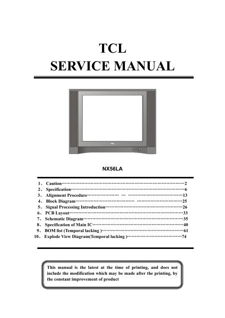
TCL SERVICE MANUAL - Tecnicosaurios
TCL SERVICE MANUAL - Tecnicosaurios
TCL SERVICE MANUAL - Tecnicosaurios

You also want an ePaper? Increase the reach of your titles
YUMPU automatically turns print PDFs into web optimized ePapers that Google loves.
<strong>TCL</strong><br />
<strong>SERVICE</strong> <strong>MANUAL</strong><br />
NX56LA<br />
1、 Caution………………………………………………………………………2<br />
2、 Specification…………………………………………………………………6<br />
3、 Alignment Procedure………………… … ………………………………13<br />
4、 Block Diagram………………………………… …………………………25<br />
5、 Signal Processing Introduction……………………………………………26<br />
6、 PCB Layout…………………………………………………………………33<br />
7、 Schematic Diagram…………………………………………………………35<br />
8、 Specification of Main IC……………………………………………………40<br />
9、 BOM list (Temporal lacking )………………………………………………61<br />
10、 Explode View Diagram(Temporal lacking )………………………………74<br />
This manual is the latest at the time of printing, and does not<br />
include the modification which may be made after the printing, by<br />
the constant improvement of product
1、<br />
CAUTION:<br />
Use of controls, adjustments or procedures other than those specified herein may result in<br />
hazardous radiation exposure.<br />
CAUTION<br />
RISK OF ELECTRIC<br />
SHOCK DO NOT OPEN.<br />
CAUTION: TO REDUCE THE RISK OF<br />
ELECTRICAL SHOCK, DO NOT REMOVE<br />
COVER (OR BACK). NO USER <strong>SERVICE</strong>ABLE<br />
PARTS INSIDE. REFER SERVICING TO<br />
QUALIFIED <strong>SERVICE</strong> PERSONNEL.<br />
The lighting flash with arrowhead symbol, with an equilateral triangle is intended to<br />
alert the user to the presence of uninsulated dangerous voltage within the products<br />
enclosure that may be of sufficient magnitude to constitute a risk of electric shock to<br />
the person.<br />
The exclamation point within an equilateral triangle is intended to alert the user to the<br />
presence of important operating and maintenance (servicing) instructions in the<br />
literature accompanying the appliance.<br />
WARNING: TO REDUCE RISK OF FIRE OR ELECTRIC SHOCK, DO NOT<br />
EXPOSE THIS APPLIANCE TO RAIN OR MOISTURE.<br />
2
IMPORTANT SAFETY INSTRUCTIONS<br />
CAUTION:<br />
Read all of these instructions. Save these instructions for later use. Follow all Warnings and<br />
Instructions marked on the audio equipment.<br />
1. Read Instructions- All the safety and operating instructions should be read before the product is operated.<br />
2. Retain Instructions- The safety and operating instructions should be retained for future reference.<br />
3. Heed Warnings- All warnings on the product and in the operating instructions should be adhered to.<br />
4. Follow Instructions- All operating and use instructions should be followed.<br />
FOR YOUR PERSONAL SAFETY<br />
1. When the power cord or plug is damaged or frayed, unplug this television set from the wall outlet and refer servicing to<br />
qualified service personnel.<br />
2. Do not overload wall outlets and extension cords as this can result in fire or electric shock.<br />
3. Do not allow anything to rest on or roll over the power cord, and do not place the TV where power cord is subject to<br />
traffic or abuse. This may result in a shock or fire hazard.<br />
4. Do not attempt to service this television set yourself as opening or removing covers may expose you to dangerous<br />
voltage or other hazards. Refer all servicing to qualified service personnel.<br />
5. Never push objects of any kind into this television set through cabinet slots as they may touch dangerous voltage<br />
points or short out parts that could result in a fire or electric shock. Never spill liquid of any kind on the television set.<br />
6. If the television set has been dropped or the cabinet has been damaged, unplug this television set from the wall outlet<br />
and refer servicing to qualified service personnel.<br />
7. If liquid has been spilled into the television set, unplug this television set from the wall outlet and refer servicing to<br />
qualified service personnel.<br />
8. Do not subject your television set to impact of any kind. Be particularly careful not to damage the picture tube surface.<br />
9. Unplug this television set from the wall outlet before cleaning. Do not use liquid cleaners or aerosol cleaners. Use a<br />
damp cloth for cleaning.<br />
10.1. Do not place this television set on an unstable cart, stand, or table. The television set may fall, causing serious injury<br />
to a child or an adult, and serious damage to the appliance. Use only with a cart or stand recommended by the<br />
manufacturer, or sold with the television set. Wall or shelf mounting should follow the manufacturer s instructions, and<br />
should use a mounting kit approved by the manufacturer.<br />
10.2. An appliance and cart combination should be moved with care. Quick stops, excessive force, and uneven surfaces<br />
may cause the appliance and cart combination to overturn.<br />
3
PROTECTION AND LOCATION OF YOUR SET<br />
11. Do not use this television set near water ... for example, near a bathtub, washbowl, kitchen sink, or laundry tub, in a<br />
wet basement, or near a swimming pool, etc.<br />
Never expose the set to rain or water. If the set has been exposed to rain or water, unplug the set from the wall<br />
outlet and refer servicing to qualified service personnel.<br />
12. Choose a place where light (artificial or sunlight) does not shine directly on the screen.<br />
13. Avoid dusty places, since piling up of dust inside TV chassis may cause failure of the set when high humidity persists.<br />
14. The set has slots, or openings in the cabinet for ventilation purposes, to provide reliable operation of the receiver, to<br />
protect it from overheating. These openings must not be blocked or covered.<br />
Never cover the slots or openings with cloth or other material.<br />
Never block the bottom ventilation slots of the set by placing it on a bed, sofa, rug, etc.<br />
Never place the set near or over a radiator or heat register.<br />
Never place the set in a built-in enclosure, unless proper ventilation is provided.<br />
PROTECTION AND LOCATION OF YOUR SET<br />
15.1. If an outside antenna is connected to the television set, be sure the antenna system is grounded so as to provide some<br />
protection against voltage surges and built up static charges, Section 810 of the National Electrical Code, NFPA No.<br />
70-1975, provides information with respect to proper grounding of the mast and supporting structure, grounding of the<br />
lead-in wire to an antenna discharge unit, size of grounding conductors, location of antenna discharge unit, connection<br />
to grounding electrode, and requirements for the grounding electrode.<br />
EXAMPLE OF ANTENNA GROUNDING AS PER NATIONAL ELECTRICAL CODE INSTRUCTIONS<br />
EXAMPLE OF ANTENNA GROUNDING AS PER<br />
NATIONAL ELECTRICAL CODE<br />
ANTENNA<br />
LEAD- IN WIRE<br />
GROUND CLAMP<br />
ANTENNA DISCHARGE<br />
UNIT (NEC SECTION<br />
810-20)<br />
ELECTRIC <strong>SERVICE</strong><br />
EQUIPMENT<br />
GROUNDING<br />
CONDUCTORS<br />
(NEC SECTION810-21)<br />
GROUND CLAMPS<br />
NEC-NATIONAL ELECTRICAL CODE<br />
POWER <strong>SERVICE</strong> GROUNDING<br />
ELECTRODE SYSTEM<br />
(NEC ART 250. PART H)<br />
15.2. Note to CATV system installer : (Only for the television set with CATV reception)<br />
This reminder is provided to call the CATV system installer s attention to Article 820-40 of the NEC that provides<br />
guidelines for proper grounding and, in particular, specifies that the cable ground shall be connected to the grounding<br />
system of the building, as close to the point of cable entry as practical.<br />
16. An outside antenna system should not be located in the vicinity of overhead power lines or other electric lights or power<br />
circuits, or where it can fall into such power lines or circuits. When installing an outside antenna system, extreme care<br />
should be taken to keep from touching such power lines or circuits as contact with them might be fatal.<br />
17. For added protection for this television set during a lightning storm, or when it is left unattended and unused for long<br />
periods of time, unplug it from the wall outlet and disconnect the antenna. This will prevent damage due to lightning<br />
and power-line surges.<br />
4
OPERATION OF YOUR SET<br />
18. This television set should be operated only from the type of power source indicated on the marking label. If you are not<br />
sure of the type of power supply at your home, consult your television dealer or local power company. For television<br />
sets designed to operate from battery power, refer to the operating instructions.<br />
19. If the television set does not operate normally by following the operating instructions, unplug this television set from the<br />
wall outlet and refer servicing to qualified service personnel. Adjust only those controls that are covered in the operating<br />
instructions as improper adjustment of other controls may result in damage and will often require extensive work by a<br />
qualified technician to restore the television set to normal operation.<br />
20. When going on a holiday : If your television set is to remain unused for a period of time, for instance, when you go on<br />
a holiday, turn the television set off and unplug the television set from the wall outlet.<br />
IF THE SET DOES NOT OPERATE PROPERLY<br />
21. If you are unable to restore normal operation by following the detailed procedure in your operating instructions,<br />
do not attempt any further adjustment. Unplug the set and call your dealer or service technician.<br />
22. Whenever the television set is damaged or fails, or a distinct change in performance indicates a need for<br />
service, unplug the set and have it checked by a professional service technician.<br />
23. It is normal for some TV sets to make occasional snapping or popping sounds, particularly when being<br />
turned on or off. If the snapping or popping is continuous or frequent, unplug the set and consult your<br />
dealer or service technician.<br />
FOR <strong>SERVICE</strong> AND MODIFICATION<br />
24. Do not use attachments not recommended by the television set manufacturer as they may cause hazards.<br />
25. When replacement parts are required, be sure the service technician has used replacement parts specified<br />
by the manufacturer that have the same characteristics as the original part. Unauthorized substitutions<br />
may result in fire, electric shock, or other hazards.<br />
26. Upon completion of any service or repairs to the television set, ask the service technician to perform<br />
routine safety checks to determine that the television is in safe operating condition.<br />
5
<strong>TCL</strong>-Thomson Electronics R&D Center (Shen’Zhen Lab)<br />
Product Functional Specification<br />
Chassis Name<br />
Issued On<br />
Updated On<br />
NX56-LA<br />
Serial No.<br />
2008-5-19 Page<br />
1 of 7<br />
Version<br />
1.0
TTE Corporation R&D Center (Shen’Zhen Lab)<br />
Disclosure<br />
Proprietary Information: These drawings and specifications are the property of <strong>TCL</strong>-Thomson Electronics and shall not be<br />
reproduced or copied or used as the basis for the manufacture or sale of apparatus or devices without the written<br />
permission of <strong>TCL</strong>-Thomson Electronics.<br />
Version Information: Version states by two Arabic Numbers, which is separated by one dot, e.g. 1.2. The first number “1”<br />
means the version of approved file, the second one ”2” means the version of draft.<br />
Chassis Name<br />
Issued On<br />
Updated On<br />
NX56-LA<br />
Serial No.<br />
2008-5-19 Page<br />
2 of 7<br />
Version<br />
1.0
TTE Corporation R&D Center (Shen’Zhen Lab)<br />
Revision History<br />
Model No.<br />
29185<br />
Date<br />
Prepared by lipeng 2008.5.19<br />
Checked by<br />
Status<br />
Comment<br />
V1.0<br />
03-B185SAE-SC31<br />
21M63US<br />
Released by:<br />
Prepared by lipeng 2008.5.19<br />
Checked by<br />
Released by:<br />
Revised by<br />
Checked by<br />
Released by:<br />
Revised by<br />
Checked by<br />
Released by:<br />
V1.0<br />
03-DM63SAE-SC31S<br />
Chassis Name<br />
Issued On<br />
Updated On<br />
NX56-LA<br />
2008-5-19<br />
Serial No.<br />
Page<br />
3 of 7<br />
Version 1.0
TTE Corporation R D Center (Shen’Zhen Lab)<br />
Item<br />
Model<br />
NX56-LA<br />
29185<br />
NX56-LA<br />
21M63US<br />
Master Data<br />
-Version 1 1<br />
-Customer ID EM EM<br />
-Destination EM EM<br />
-Brand<br />
-BOM NO. 03-B185SAE-SC31 03-DM63SAE-SC31S<br />
-Chassis<br />
Reception<br />
-Tuning [Channels Amt.] 181 181<br />
-Tuning [Technology] PLL PLL<br />
-Tuning [Indication] Channel Channel<br />
-Frequency Bands Antenna AND Cable Antenna AND Cable<br />
-IF Frequency 45.7MHz 45.7MHz<br />
-TV Systems (Color+ Sound) PAL M/N NTSC M PAL M/N NTSC M<br />
-AV Systems NTSC PAL NTSC PAL<br />
Picture-Processing<br />
-SCAN Standard Standard<br />
-Wide Screen Switching<br />
-Comb filter<br />
-Picture Enhancement<br />
LTI / CTI<br />
Black Stretch<br />
Dynamic Skin<br />
Others<br />
-Picture Control [General]<br />
Brightness X X<br />
Sharpness X X<br />
Contrast X X<br />
Tint X X<br />
Color X X<br />
-Picture Control [Special]<br />
Smart Pictures * modes 4 modes 4 modes<br />
VM<br />
Color Temperature 3 modes 3 modes<br />
Others<br />
-Picture Noise Reduction X X<br />
Picture – Display<br />
-CRT Type<br />
Normal Flat<br />
Pure Flat X X<br />
Super Flat<br />
-Deflection system<br />
1Fh X X<br />
2Fh<br />
-Tube Technology<br />
Iron<br />
AK X X<br />
Black Matrix<br />
Others<br />
-CRT Deflection ( * Deg.) 110 120<br />
-CRT Magnetic Field<br />
-Screen Type 4:3 4:3<br />
-Screen Size / Vis. Size 29' 21' Super Slim<br />
Sound<br />
-Audio Power Consumption 5W+5W 4W+4W<br />
-Surround Sound<br />
Chassis: NX56-LA Version: 1.0
TTE Corporation R D Center (Shen’Zhen Lab)<br />
Item<br />
Model<br />
NX56-LA<br />
29185<br />
NX56-LA<br />
21M63US<br />
-Nicam<br />
-America Stereo (MTS,BTSC,MPS) X X<br />
-America SAP<br />
-Korea Stereo<br />
-Thai Bilingual<br />
-Super Woofer<br />
-AVL<br />
-Sound Control [General]<br />
Volume X X<br />
Mute X X<br />
-Sound Control [Special]<br />
Treble<br />
Bass<br />
Balance X X<br />
Equalizer<br />
Smart Sound * modes<br />
Others<br />
-Speakers Quantity 2X1 2X1<br />
User Interface<br />
-Menu Language English/Portugal/Espanol English/Portugal/Espanol<br />
-Features [General]<br />
AT<br />
Biological Clock<br />
Calendar<br />
Clock<br />
Channel Swap X X<br />
Channel Naming<br />
Child Lock X X<br />
Favorite Channel X X<br />
Game<br />
Hotel Mode X X<br />
High Sensitive<br />
Notebook<br />
On/Off Timer<br />
Preset X X<br />
Recall X X<br />
Rotation<br />
Sleep X X<br />
AVC<br />
-Features [Special]<br />
V-chip / CCD X X<br />
Teletext *Pages<br />
Others<br />
New Features<br />
Smart signal<br />
Voltage display<br />
环 境 光 检 测<br />
Easy search<br />
Tuning Features<br />
-Auto Channel Program X X<br />
-Auto/Manual Tuning X X<br />
-Auto/Manual Store X X<br />
-Fine Tuning X X<br />
-Factory Mode X X<br />
-Service Mode<br />
Cabinet<br />
-Cabinet Name<br />
Chassis: NX56-LA Version: 1.0
TTE Corporation R D Center (Shen’Zhen Lab)<br />
Item<br />
Model<br />
NX56-LA<br />
29185<br />
NX56-LA<br />
21M63US<br />
-Front Cabinet Color<br />
-Middle Cabinet Color<br />
-Rear Cabinet Color<br />
-Local Controls Front<br />
Mains Switch X X<br />
CH+ CH- VOL+ VOL- X X<br />
TV/AV X X<br />
Menu X X<br />
Auto Search<br />
-Local Controls Top<br />
CH+ CH- VOL+ VOL-<br />
TV/AV<br />
Menu<br />
Auto Search<br />
-Indicator<br />
RC Received LED X X<br />
Standby LED X X<br />
Remote Controller<br />
-Type RC166 RC166<br />
-Batteries<br />
Connectors Rear<br />
-SCART Full w/o Y/C<br />
-SCART Full with Y/C<br />
-SCART Single (CVBS)<br />
-Component In (YPbPr) Cinch for 50Hz<br />
-In Y/C+Cinch(CVBS+ Stereo) 1 + 1 1 + 2<br />
-In Y/C+Cinch (CVBS+ Mono)<br />
-In Cinch(CVBS+ Stereo)<br />
-In Cinch (CVBS+ Mono)<br />
-Out Cinch(CVBS+ Stereo)<br />
-Out Cinch(CVBS+ Mono) 1(follow TV) 1(follow TV)<br />
- Y,Cb,Cr input X X<br />
-Super Woofer<br />
-Digital Audio Out<br />
-Loudspeakers<br />
-Control Busses<br />
-Feature Slot<br />
-ITV Smart Port<br />
- Antenna in<br />
75 Ohms (F Type) X X<br />
Connectors Front/Side<br />
-In Y/C+Cinch(CVBS+ Stereo)<br />
-In Y/C+Cinch (CVBS+ Mono)<br />
-In Cinch(CVBS+ Stereo)<br />
X<br />
-In Cinch (CVBS+ Mono)<br />
-Out Headphone<br />
Mini-Jack 3.5mm<br />
Final Equipment<br />
-Packing –Methods<br />
2 Color Printing<br />
Carton Color<br />
-Documents and Manuals<br />
Instruction Book<br />
Screen Sticker<br />
Plastic Bag<br />
Warranty Card<br />
Chassis: NX56-LA Version: 1.0
TTE Corporation R D Center (Shen’Zhen Lab)<br />
Item<br />
Model<br />
NX56-LA<br />
29185<br />
NX56-LA<br />
21M63US<br />
Guarantee Doc.<br />
Warning Label<br />
Approbation Label<br />
Others<br />
-Languages DFU<br />
-Indication on BACKOVER<br />
Made-in in family sheet<br />
FCC/Elect Shock Caution Label<br />
CE/Elect Shock Caution Label<br />
Warning Label<br />
Others<br />
Approbation<br />
IEC65<br />
IEC65<br />
Miscellaneous<br />
-Mains Voltage 100-240V 100-240V<br />
-Mains Frequency 50/60Hz 50/60Hz<br />
-Type Mains Cord<br />
-Power Consumption TV in ON 75W 75W<br />
-Power Consumption TV in Standby
<strong>TCL</strong>-THOMSON Electronics R&D Center (Shen’Zhen Lab)<br />
NX56-LA Chassis<br />
Alignment Procedure<br />
Chassis Name NX56-LA Serial No.<br />
Issued on 2008-05-19 Page Page 1 of 12<br />
Updated on Version 1.0
<strong>TCL</strong>-THOMSON Electronics R&D Center (Shen’Zhen Lab)<br />
Disclosure<br />
Proprietary Information: These drawings and specifications are the<br />
property of <strong>TCL</strong>-Thomson Electronics and shall not be reproduced or<br />
copied or used as the basis for the manufacture or sale of apparatus or<br />
devices without the written permission of <strong>TCL</strong>-Thomson Electronics.<br />
Version Information: Version states by two Arabic Numbers, which is<br />
separated by one dot, e.g. 1.2. The first number “1” means the version of<br />
approved file, the second one ”2” means the version of draft.<br />
Chassis Name NX56-LA Serial No.<br />
Issued on 2008-05-19 Page Page 2 of 12<br />
Updated on Version 1.0
<strong>TCL</strong>-THOMSON Electronics R&D Center (Shen’Zhen Lab)<br />
Revision History<br />
Model No. Status Date Comment<br />
Prepared by LIPENG 2008-05-15<br />
03-B185SAE-SC31<br />
29185 Checked by<br />
(29185/NX56-LA)<br />
Released by<br />
Prepared by LIPENG 2008-05-15<br />
03-DM62SAE-SC31S<br />
21M63US Checked by<br />
(21M63US/NX56-LA)<br />
Released by<br />
Revised by<br />
Checked by<br />
Released by<br />
Revised by<br />
Checked by<br />
Released by<br />
Revised by<br />
Checked by<br />
Released by<br />
Revised by<br />
Checked by<br />
Released by<br />
Chassis Name NX56-LA Serial No.<br />
Issued on 2008-05-19 Page Page 3 of 12<br />
Updated on Version 1.0
<strong>TCL</strong>-THOMSON Electronics R&D Center (Shen’Zhen Lab)<br />
1.1. The way to enter P-Mode<br />
a) Method one<br />
A) Switch on the TV set.<br />
B) Press the “MENU” key on RC to show the “PICTURE” OSD menu.<br />
C) Move the cursor to “Contrast” item then press the “9”, “7”, “3”, “5” key<br />
continuously on RC within 3 seconds then enter P-Mode. The “P” letter will<br />
appear on the left low corner of the screen when enter P-Mode. Also the<br />
“FACTORY HOTKEY” will be set to “ON ( = 1 )”.<br />
b) Another method<br />
Press the “RECALL” key on RC to enter P-mode directly.<br />
*Notes:<br />
1. This will be active only when the “FACTORY HOTKEY” had set to “ON ( = 1 )”.<br />
2. When the power on with “FACTORY HOTKEY” had set to “ON ( = 1 )”, the set<br />
will enter the P-Mode automatically.<br />
1.2. Exit the P-Mode<br />
Press the “RECALL” or “MENU” key on RC to exit the P-Mode.<br />
1.3. Keys’ function on RC at the P-Mode<br />
Use the RC to navigate in P-Mode:<br />
Press “0” to “9” key to select factory adjustment page.<br />
Press “▲▼” key to select option.<br />
Press “►◄” key to adjust or select option.<br />
Press “DISPLAY” key to display software version.<br />
Press “MENU” key to exit the P-Mode.<br />
Press “RECALL” key to enter or exit the P-Mode.<br />
All change in P-Mode will be saved in EEPROM automatically<br />
1.4. The adjustment page list on P-Mode:<br />
RC key Item Description<br />
0 Screen voltage adjustment<br />
1 Picture Geometric adjustment 1 Vertical geometry<br />
2 Picture Geometric adjustment 2 Horizontal geometry<br />
3 White Balance Adjustment<br />
4 Setup 1<br />
5 Setup 2<br />
6 Setup 3<br />
7 Setup 4<br />
8 Setup 5<br />
9 I2C Bus OFF<br />
Press this key to enter or exit BUS<br />
OFF mode<br />
DISPLAY Display software version<br />
Chassis Name NX56-LA Serial No.<br />
Issued on 2008-05-19 Page Page 4 of 12<br />
Updated on Version 1.0
<strong>TCL</strong>-THOMSON Electronics R&D Center (Shen’Zhen Lab)<br />
2. Flowchart of alignment procedure<br />
B+ adjustment Electrical<br />
properties<br />
checking for<br />
chassis<br />
RF AGC<br />
adjustment<br />
Parameter setup<br />
White balance<br />
Aging<br />
Adjustment of<br />
Adjustment of<br />
Adjustment<br />
focus voltage<br />
screen voltaget<br />
PAL geometry<br />
NTSC<br />
Set shopping<br />
QC checking<br />
adjustment<br />
geometry<br />
status<br />
adjustment<br />
1) B+ Adjustment<br />
2) RF AGC Adjustment<br />
3) Screen & Focus adjustment<br />
4) White balance adjustment<br />
5) Producing parameter setup and option<br />
6) Picture Geometry adjustment ( Vertical first)<br />
7) Set Shopping status<br />
8) QC<br />
Chassis Name NX56-LA Serial No.<br />
Issued on 2008-05-19 Page Page 5 of 12<br />
Updated on Version 1.0
<strong>TCL</strong>-THOMSON Electronics R&D Center (Shen’Zhen Lab)<br />
3. Adjustment description<br />
*Notes: Alignment should be done after 3 minutes warm up of TV.<br />
3.1 B+ Voltages<br />
1. All relevant connectors and modules must be connected and inserted.<br />
2. Main voltage is at 220VAC, 50Hz.(voltage range:110VAC~240VAC,50Hz)<br />
3. Connect a voltmeter to B+ (Cathode of D808) and switch on the set.<br />
4. Input Philips test pattern signal and standard mode.<br />
5. Adjust VR801, it should as the value in below form B+ Voltage.<br />
Table 3.1.1: The B+ value for vary tubes<br />
CRT type (Part Number)<br />
A68ERF185X013/MS (44-29RFLT-HFCA)<br />
A51QGT420X34(44-21RFLS-LGDA)<br />
B+ Voltage<br />
125V+/-0.5V<br />
108V+/-0.5V<br />
Chassis Name NX56-LA Serial No.<br />
Issued on 2008-05-19 Page Page 6 of 12<br />
Updated on Version 1.0
<strong>TCL</strong>-THOMSON Electronics R&D Center (Shen’Zhen Lab)<br />
3.2 RF AGC alignment<br />
3.2.1 Method 1<br />
A. Connect the detector as shown below (Picture 3.2) to collector of Q101.<br />
B. Receive a grey scale signal with 70dBμV amplitude.<br />
C. Enter P-Mode, press “6” key on RC to select “AGCT”.<br />
D. Adjust AGCT item until the output of the detector becomes 0.8Vpp<br />
Collector<br />
of Q101<br />
To CRO<br />
Picture 3.2<br />
3.2.2 Method 2<br />
A. Receive a grey scale signal with 60dBμV amplitude.<br />
B. Enter P-Mode, press “6” key on RC to select “AGCT”.<br />
C. Adjust the “AGCT” value until the hint display “AGC” just change between “0” and “1”.<br />
3.3 Screen & Focus adjustment<br />
*Notes: Alignment below should be done after 15 minutes warm up of TV.<br />
1. Input cross hatch pattern signal to RF input.<br />
2. Enter P-Mode.<br />
2. Press “0” key on the RC and the screen will become a horizontal line.<br />
3. Adjust the “SCREEN” VR of the FBT until the horizontal line can just be seen barely<br />
(minimum visible intensity).<br />
4. Press “0” key again on the RC to exit the screen voltage adjustment mode.<br />
5. Adjust the “FCOUS” VR of the FBT until the vertical line and horizontal line becomes<br />
clear, like picture 3.3.<br />
Picture 3.3<br />
Chassis Name NX56-LA Serial No.<br />
Issued on 2008-05-19 Page Page 7 of 12<br />
Updated on Version 1.0
<strong>TCL</strong>-THOMSON Electronics R&D Center (Shen’Zhen Lab)<br />
3.4 White Balance Adjustment<br />
1. Input a black and white pattern to RF input.<br />
2. Enter P-Mode, press key “3 ” to select white balance adjustment menu.<br />
3. Use the color analyzer to measure the black side of the screen. Adjust the value of<br />
“RC”,”GC” and “BC” to set the reading of the color analyzer to x=274, y=280. (11500 K).<br />
4. Then measure the white side of the screen. Adjust the value of “RD”, “GD” and “BD” to<br />
set the reading of the color analyzer to x=274, y=280. (11500 K).<br />
5. Repeat step 3&4 until you can get the correct reading for both black and white sides.<br />
*Notes:<br />
A. The “SUBB” and “SubCON” items are used to assistant the white balance adjustment.<br />
It is the same function as the user OSD menu “Brightness” and “Contrast” items. You can<br />
adjust these items to get the expect intensity when adjusting the white balance.<br />
B. YUV white balance black level offset setup:<br />
It is not need to adjust the white balance for YUV mode when production, but the<br />
BLOR-Y, BLOG-Y and BLOB-Y items which locate in EEPROM address 0x0A, 0x0B and<br />
0x0C need to write in the right values to set the YUV mode black level offset before<br />
production. These offset values should be written by the PE engineer when making the<br />
EEPROM copy for the new lot with difference tube.<br />
Table 3.4.1: The White Balance adjustment OSD menu<br />
OSD menu Default Value Description Remark<br />
RC 32 R cut-off setting(BLOR) Adjust to right value<br />
GC 32 G cut-off setting(BLOG) Adjust to right value<br />
BC 32 B cut-off setting(BLOB) Adjust to right value<br />
RD 37 R drive setting(WPR) Adjust to right value<br />
GD 32 G drive setting(WPG) Adjust to right value<br />
BD 37 B drive setting(WPB) Adjust to right value<br />
BLOC 3 Black level offset course(BLOC) Recommended value= “8”<br />
PWL 8 Peak White Limiting Don’t adjust, use default<br />
BriVSD 32<br />
Brightness of horizontal line when<br />
adjust G2<br />
Don’t adjust, use default<br />
SUBB 32 Brightness<br />
Same as user “Brightness”<br />
SubCON 32 Contrast<br />
and “Contrast” adjust<br />
BRTC 31 Sub-Brightness Adjust to right value<br />
BLOR-Y 64 YUV R -OFFSET<br />
BLOG-Y 62 YUV G-OFFSET<br />
BLOB-Y 64 YUV B -OFFSET<br />
64= offset value 0 63= offset<br />
value -1 65= offset value<br />
+1 Adjust to right value<br />
3.5 Picture Geometry adjustment<br />
Chassis Name NX56-LA Serial No.<br />
Issued on 2008-05-19 Page Page 8 of 12<br />
Updated on Version 1.0
<strong>TCL</strong>-THOMSON Electronics R&D Center (Shen’Zhen Lab)<br />
3.5.1 Vertical geometry adjustment<br />
1. Input a PAL crosshatch pattern signal to RF input.<br />
2. Enter P-Mode, press key “1” to select vertical geometry adjustment. (The OSD menu<br />
for this adjustment as below table 3.5.1. For NTSC signal, the “-50” will replace with “-60”.)<br />
3. Adjust the value of the corresponding item to make the vertical geometry of the<br />
pattern look good.<br />
4. Apply NTSC signal to adjust these value for NTSC vertical geometry.<br />
Table 3.5.1: The vertical geometry adjustment OSD menu<br />
OSD menu Default Value Description Remark<br />
VSLOPE-50 32 Vertical slope(VS) Adjust to right value<br />
VCEN-50 32 Vertical shift (VSH) Adjust to right value<br />
VSIZE-50 32 Vertical amplitude(VA) Adjust to right value<br />
VZOOM-50 25 Vertical zoom(VX) Adjust to right value<br />
VSC-50 32 S-correction(SC) Adjust to right value<br />
VSCROLL-50 32 Vertical Scroll(VCS) Adjust to right value<br />
*Notes:<br />
1. For NTSC signal, the “-50” will replace with “-60”.<br />
2. For NTSC signal, only the “VCEN-60” and “VSIZE-60” items need the adjustment,<br />
the other items use the same data as PAL signal.<br />
3. On producing, please use the “AUTO OFFSET” (On page “2”) function to easy the<br />
geometry adjustment of NTSC signal. When finished the PAL signal geometry adjustment,<br />
press “2” key to enter page “2” to select “AUTO OFFSET” item, press “►” key to active the<br />
automatic offset function. Then the geometry adjustment of NTSC signal will finish<br />
automated. If the geometry of NTSC signal is look good, you don’t need to adjust the<br />
geometry of NTSC signal any more.<br />
3.5.2 Horizontal geometry adjustment<br />
1. Input a PAL crosshatch pattern signal to RF input.<br />
2. Enter P-Mode, press key “2” to select horizontal geometry adjustment. (The OSD<br />
menu for this adjustment as below table 3.5.2. For NTSC signal, the “-50” will replace with<br />
“-60”.)<br />
3. Adjust the value of the corresponding item to make the horizontal geometry of the<br />
pattern look good.<br />
4. Apply NTSC signal to adjust these value for NTSC horizontal geometry.<br />
Table 3.5.2: The horizontal geometry adjustment OSD menu<br />
OSD menu Default Value Description Remark<br />
HCEN-50 32 Horizontal shift(HSH) Adjust to right value<br />
HSIZE-50 32 EW width(EWW) Adjust to right value<br />
HPARA-50 32 EW parabola width(PW) Adjust to right value<br />
HTRAP-50 32 EW trapezium(TC) Adjust to right value<br />
HCNRT-50 32 EW upper corner parabola(UCP) Adjust to right value<br />
HCNRB-50 32 EW lower corner parabola(LCP) Adjust to right value<br />
HBOW-50 32 Horizontal bow(HB) Adjust to right value<br />
Chassis Name NX56-LA Serial No.<br />
Issued on 2008-05-19 Page Page 9 of 12<br />
Updated on Version 1.0
<strong>TCL</strong>-THOMSON Electronics R&D Center (Shen’Zhen Lab)<br />
HPARALLEL 32 Horizontal parallelogram(HP) Adjust to right value<br />
AUTO OFFSET 0 Automatic offset NTSC geometry See below description<br />
*Notes:<br />
1. For NTSC signal, the “-50” will replace with “-60”.<br />
2. For NTSC signal, only the “HCEN-60” and “HSIZE-60” items need the adjustment,<br />
the other items use the same data as PAL signal.<br />
3. On producing, please use the “AUTO OFFSET” (On page “2”) function to easy the<br />
geometry adjustment of NTSC signal. When finished the PAL signal geometry adjustment,<br />
press “2” key to enter page “2” to select “AUTO OFFSET” item, press “►” key to active the<br />
automatic offset function. Then the geometry adjustment of NTSC signal will finish<br />
automated. If now the geometry of NTSC signal is look good, it not needed to adjust the<br />
geometry of NTSC signal any more.<br />
3.6 Producing parameter setup and option<br />
1. Enter P-Mode, press key “4” to select page “4”.Set the corresponding item to require<br />
value. See below table 3.6.1 for detailed description.<br />
Table 3.6.1: Producing parameter setup and option page “4”<br />
OSD menu Default Value Description Remark<br />
WARM UP STATUS 0 Set aging mode<br />
0=Aging mode off<br />
1=Aging mode on<br />
SHOP INIT 0 Set the shopping status 0=>1= Set the shopping status<br />
DCXO 2<br />
Crystal oscillator Adjust this value to get the max<br />
frequency adjustment color synchronization range<br />
FACTORY HOTKEY 1 Set factory hotkey<br />
0=”FACTORY HOTKEY” off<br />
1=”FACTORY HOTKEY” on<br />
POWER ON MODE LAST Set the power on mode<br />
ON=On when power on<br />
STB=Standby when power on<br />
LAST=Last power off status<br />
EEPROM INIT 0 EEPROM initial 0=>1=Active EEPROM initial<br />
2. Enter P-Mode, press key “5” to select page “5”. Set the corresponding item to require<br />
value. See below table 3.6.2 for detailed description.<br />
Table 3.6.2: Producing parameter setup and option page “5”<br />
OSD menu Default Value Description Remark<br />
Track. Mode 1 EHT tracking mode<br />
0=EHT tracking only on vertical<br />
1=EHT tracking on vertical and EW<br />
VX Normal 25 4:3 mode vertical zoom Don’t adjust, use default<br />
Chassis Name NX56-LA Serial No.<br />
Issued on 2008-05-19 Page Page 10 of 12<br />
Updated on Version 1.0
<strong>TCL</strong>-THOMSON Electronics R&D Center (Shen’Zhen Lab)<br />
VX Compr. 0 16:9 mode vertical zoom Don’t adjust, use default<br />
WBF 5 Wide blanking start Don’t adjust, use default<br />
WBR 8 Wide blanking end Don’t adjust, use default<br />
GET OFFSET 0 Get offset See below description<br />
ColdRD 60 Cold color temperature R 64= offset value 0 63= offset value<br />
ColdGD 59<br />
and G drive offset -1 65= offset value +1 Adjust to<br />
right value<br />
WarmRD 74 Warm color temperature R 64= offset value 0 63= offset value<br />
WarmGD 71<br />
and G drive offset -1 65= offset value +1 Adjust to<br />
right value<br />
Description for AUTO OFFSET and GET OFFSET:<br />
The “GET OFFSET” can use to make the EEPROM copy by PE engineer. When the<br />
PAL and NTSC geometry adjustment had finished, trigger the “GET OFFSET” from “0” to<br />
“1” to store the geometry offset datum between PAL and NTSC in EEPROM.<br />
On producing, these geometry offset datum can use to easy the NTSC geometry<br />
adjustment. When finished the PAL geometry adjustment, trigger the “AUTO OFFSET”<br />
from “0” to “1”, then the geometry adjustment of NTSC signal will finish automated. If now<br />
the geometry of NTSC signal is look good, it not needed to adjust the geometry of NTSC<br />
signal any more.<br />
3. Enter P-Mode, press key “6” to select page “6”. Set the corresponding item to require<br />
value. See below table 3.6.3 for detailed description.<br />
Table 3.6.3: Producing parameter setup and option page “6”<br />
OSD menu Default Value Description Remark<br />
AGCT 32 AGC take over point See section “3.2 RF AGC alignment”<br />
AGC 0 AGC take over point indicate for detailed.<br />
OIF 32 IF demodulator offset Don’t adjust, use default<br />
IF 45.7 IF frequency Select the IF frequency<br />
AGCS 1 AGC speed Don’t adjust, use default<br />
AGNE 3 Audio gain Don’t adjust, use default<br />
4. Enter P-Mode, press key “7” to select page “7”. Set the corresponding item to require<br />
value. See below table 3.6.4 for detailed description.<br />
Table 3.6.4: Producing parameter setup and option page “7”<br />
OSD menu Default Value Description Remark<br />
EVG 0 Enable vertical guard(RGB blanking) 1= RGB blanking<br />
DFL 0 Disable flash protection from defletion timer Don’t adjust, use default<br />
Chassis Name NX56-LA Serial No.<br />
Issued on 2008-05-19 Page Page 11 of 12<br />
Updated on Version 1.0
<strong>TCL</strong>-THOMSON Electronics R&D Center (Shen’Zhen Lab)<br />
XDT 0 X-ray detection Don’t adjust, use default<br />
AKB 1 Black current stabilization Don’t adjust, use default<br />
NBL 1 Black current loop application Don’t adjust, use default<br />
OSVE 0<br />
Black current measuring lines in over<br />
scan(for vertical zoom setting
Chapter II Block Diagram of NX56 July5,2008<br />
220VAC<br />
INPUT<br />
Bridge<br />
Rectifier<br />
DB801-<br />
DB804<br />
Power<br />
Transistor<br />
Q801<br />
2SK2996<br />
Transformer<br />
T801<br />
B 33V<br />
+-14V<br />
12V<br />
9V<br />
Q501<br />
Q503<br />
Q505<br />
AMP<br />
CRT<br />
▽ Antenna<br />
Tuner<br />
TU101<br />
IF AMP<br />
Q101<br />
IC801<br />
NCP1337<br />
SAW Z2O1<br />
Photo-Coupler<br />
IC803<br />
Pin44-46<br />
P201<br />
R/G/B<br />
V.AMP.<br />
IC301<br />
STV8172A<br />
SCA/SDL<br />
EEPROM<br />
IC001<br />
Pin14/15<br />
VDA/B<br />
Pin 56<br />
H.OUT<br />
P901<br />
TV/AV/SV B+<br />
pin21<br />
P202<br />
KEY &IR001<br />
SENSOR<br />
UOC IC201<br />
IC701 AN5832SA<br />
Aout -L/R<br />
IC702 74HC4053<br />
Audio<br />
AMP.<br />
IC601<br />
TDA7266SA<br />
H.Driver<br />
AMP Q401<br />
Q402<br />
FBT T401<br />
speakerX2<br />
200V<br />
24V<br />
6.3V
NX56 Chassis Signal Processing Introduction<br />
Brief introduction<br />
For different market requirements, our design it in two versions, one is<br />
for Latin America, we call the chassis as NX56-LA, the another one is for<br />
Asia Pacific Area, we call the chassis as NX56-AP. NX56-LA and<br />
NX56-AP adopt different UOC, The UOC for Latin America have<br />
CCD-Chip and BTSC function, so added AN5832SA to realize BTSC,<br />
but the UOC for Asia Pacific region does not have the two functions but<br />
SECAM system is necessary. NX56 Chassis not only match 21inches<br />
CRT, but also match 25 and 29inches CRT. Due to different screen sizes,<br />
maybe adopt different audio power amplifiers. The others should be the<br />
same. No matter NX56-AP what NX56-LA, they are use same main PCB<br />
board, just different peripheral components.
RF Section<br />
Tuner Tu101 receive the radio frequency signal, after inside circuit to do<br />
signal receiving, and signal amplifying. The amplified high frequency<br />
signal accompany with the high frequency oscillation voltage oscillated<br />
by set oscillator input to the mixer. The IF picture signal and sound signal<br />
formed in mixer and output from mixer, then send to picture IF<br />
processing circuit.<br />
VGA<br />
(Fig. 1. Tuner section)
Small Signal Processing Section<br />
Small signal processing section is the IF (intermediate frequency) signal across saw filter send in<br />
the pin12 and pin13 of IC201. The VIFIN signal through built-in PLL DEMOD, sound trap, video<br />
amplifier and synchronous detector processing, get the color video broadcast signal and 2 nd sound<br />
IF signal.<br />
Video signal processing section is CVBS across video filter and delay line and horizontal &<br />
vertical synchronous separation circuit processing and get H-drive (pin56 of IC201)and V-drive<br />
signal (pin15/pin15 of IC201).<br />
IF sound signal across the sound-down-mixer and AM demodulator processing, send out the AVL/<br />
SSIF OUT signal. ( Refer to Fig2 and Fig 3.)<br />
(Fig 2. Small Signal Processing Section)
(Fig3. Block Diagram of IC201.)<br />
Horizontal Scanning Section<br />
The horizontal drive signal send out from pin 56 of IC201, Q401 is horizontal driving transistor,<br />
coupled by horizontal driving transformer T402 , to control the horizontal output transistor<br />
working in switch on and off situation, get good linearly and enough amplitude of saw-tooth wave<br />
current to drive horizontal deflection yoke scanning. L456 is horizontal width coil and L458 is<br />
horizontal linearly coil. D455 is damping diode, C453,C455,C457 are retrace capacitors. T401 is<br />
FBT. Pin2 of T401 is B+ voltage input, Pin 10 of T401 get 200 Volt video amplifying voltage<br />
supply for CRT board. Pin11 of T401 sends out heater voltage supply for CRT heater.
Vertical Scanning Section<br />
Vertical scanning section adopted STV8172A vertical deflection booster, we use as<br />
differential-output driver. The vertical raw-tooth wave signal sends out from pin14/15 of IC201<br />
VDA/VDB. The two differential signal input pin 1 and 7 of STV8172A IC301. Pin2(+14v) and<br />
Pin7(-14v) of IC301 is power supply which come from the main power transformer. Pin 6 is boost<br />
voltage, rectified by D301. C309,C301 and R305 makes up a voltage feedback network, R306 is a<br />
damping resistor. C306 is correction capacitor, R308 is current feedback resistor.<br />
Fig 4. Vertical Scanning Processing Section<br />
CRT Scanning Section<br />
Q507,D501,D502 and D503 makes up a light eliminate circuit network. When the TV is playing<br />
mode, +8V voltage across R533 charge for C512, Q507 is cut off. At the right of turn off the TV,<br />
Q507 is turn-on, the current across D501, D502 and D503 send to R.G. B to discharge the<br />
electronic quickly.
Audio Power Amplifying Section<br />
Power Supply Section<br />
AC supply 220V/110v through filtering network and rectifying circuit and get 300Vdc voltage.<br />
LF801/LF801A and CX802 makes up a differential mode rejection, LF802 and CY801,CY802<br />
makes up a common mode rejection network. D801-D804 is rectifying network. 300Vdc voltage<br />
supply pin3 of T801, also through R804 send to pin8 of IC801 NCP1337. Pin5 of IC801 sends out<br />
the PWM signal to control Q801 working in switch on and off situation. IC803 is optocoupler.
$1I567
UOC-TOP-64 N1 series<br />
Versatile signal processor for CRT TV applications<br />
Rev. 0.11 — 25 January 2007<br />
Product data sheet<br />
1. General description<br />
The UOC-TOP-64 series is a very flexible concept which offers attractive solutions for 1f H<br />
TV receivers with CRTs. This new concept offers a complete range of products with the<br />
right price level to cover TV receivers from basic mono 14 inch sets up to the best<br />
featured large and/or wide screen AV-stereo TV sets. The UOC-TOP-64 concept can also<br />
be used as front-end for 2f H and LCD TV receivers.<br />
The UOC-TOP-64 concept is mounted in a SDIP64 package and is split up in the following<br />
ranges:<br />
• AV-110 (AV-stereo) concept. It contains a video processor with many features and it<br />
has an analog audio control circuit with balance, treble, bass and loudness control.<br />
Two different micro processor are available for this concept, one with OSD and<br />
Closed Captioning or Teletext and Closed Captioning features (UOCTOP_1PTXT<br />
version), the other with (extended) OSD features (UOCTOP_OSD version). The block<br />
diagram is given in Figure 1.<br />
• AV-90 concept. This concept is nearly identical to the AV-110 concept. The only<br />
difference that it does not contain an East-West and Scan Velocity Modulation (SVM)<br />
output. This concept is intended for 90× picture tubes.<br />
• Mono-110 concept. The functional content of this concept is comparable with that of<br />
the AV 110 concept, however, it has just stereo input switch and no audio control<br />
circuit. The block diagram is given in Figure 1.<br />
• Mono-90 concept. This concept is intended for 90× picture tubes. The circuit has an<br />
audio switch for mono signals but the mono inputs can also be used as a stereo input.<br />
In this range most of the video and audio processing features have been omitted. Also<br />
this concept can be supplied with one of the two micro processors (UOCTOP_1PTXT<br />
or UOCTOP_OSD version). The block diagram is given in Figure 2.<br />
The most important features of the complete IC series are given in the following feature<br />
lists.<br />
All packages are according to the ROHS legislation, which also means that these<br />
packages are lead-free. The ICs have supply voltages of 8V, 5V and 3.3V.<br />
UOC-TOP-64 is supported by a comprehensive Global TV Software Development kit to<br />
enable easy programming and fast time-to-market (see also Section 20.4 “Licenses”).
NXP Semiconductors<br />
UOC-TOP-64 N1 series<br />
Signal processor for CRT TV<br />
2. Features<br />
2.1 Analog Video Processing<br />
2.1.1 Overview of available features (AV-110/90 and Mono-110 concept)<br />
• Multi-standard vision IF circuit with alignment-free PLL demodulator<br />
• Internal (switchable) time-constant for the IF-AGC circuit<br />
• Switchable group delay correction and sound trap (with switchable centre frequency)<br />
for the demodulated CVBS signal<br />
• Separate Second Sound IF output or FM demodulator output without de-emphasis<br />
available, which can be used as input for an external BTSC decoder or as input for<br />
external sound band-pass filter for second language processing.<br />
• Separate SSIF input available as input for the FM-PLL demodulator to demodulate<br />
FM-radio with an IF frequency of 10.7 MHz, or as input from an external sound<br />
band-pass filter for second language processing.<br />
• AM demodulator without extra reference circuit<br />
• The mono intercarrier sound circuit has a selective FM-PLL demodulator which can be<br />
switched to the different FM sound frequencies (4.5/5.5/6.0/6.5 MHz). The quality of<br />
this system is such that the external band-pass filters can be omitted.<br />
• The FM-PLL demodulator can be set to centre frequencies of 4.72/5.74 MHz so that a<br />
second sound channel can be demodulated. In such an application it is necessary that<br />
an external bandpass filter is inserted.<br />
• Audio switch circuit with 2 stereo inputs (1 stereo input can also be switched into two<br />
mono sound inputs) and a stereo output which can be used for the drive of for audio<br />
power amplifiers (with volume and tone-control) or as SCART/CINCH output. The<br />
second stereo input is only available via the combined C2/C3/C4/AUDIOIN5R pin for<br />
the right channel and via the combined CVBS4/Y4/AUDIOIN5L pin for the left channel.<br />
• Video switch with 3 external CVBS inputs. All CVBS inputs can be used as Y-input for<br />
Y/C signals. However, only 1 Y/C source can be selected because the circuit has 1<br />
chroma input. CVBS3/Y3 input available in combination with the G/Y-3 input pin.<br />
• 1 CVBS output, this output can be used as monitor video output or as front-end video<br />
output or as independent selectable video output.<br />
• Automatic Y/C signal detector.<br />
• Integrated luminance delay line with adjustable delay time<br />
• Only one reference (24.576 MHz) crystal required for the m-Controller, Teletext- and<br />
the color decoder<br />
• Multi-standard color decoder with automatic search system and various “forced mode”<br />
possibilities<br />
• Internal base-band delay line<br />
• Indication of the Signal-to-Noise ratio of the incoming CVBS signal<br />
• Linear RGB/YP B P R input.<br />
• Scan Velocity Modulation output. The SVM circuit is active for all the incoming CVBS,<br />
Y/C and RGB/YP B P R signals. The SVM output is combined with the black current input<br />
of the black current stabilisation circuit. By means of a small application adaptation<br />
both functions can be operational in parallel.<br />
<br />
© NXP B.V. 2007. All rights reserved.<br />
Product data sheet Rev. 0.11 — 25 January 2007 2 of 230
NXP Semiconductors<br />
UOC-TOP-64 N1 series<br />
Signal processor for CRT TV<br />
• Picture improvement features with peaking (with switchable centre frequency,<br />
depeaking, variable positive/negative peak ratio, variable pre-/overshoot ratio and<br />
video dependent coring), dynamic skin tone control, gamma control and blue- and<br />
black stretching. All features are available for CVBS, Y/C and RGB/YP B P R signals<br />
• The effect of the various features can de demonstrated by means of a ‘split screen’<br />
mode in which the features are activated in one half of the picture and switched off in<br />
the other half<br />
• Switchable DC transfer ratio for the luminance signal<br />
• Tint control for external RGB/YP B P R signals<br />
• Contrast reduction possibility during mixed-mode of OSD and Text signals. Option to<br />
make a colored and in contrast reduced window.<br />
• RGB control circuit with ‘Continuous Cathode Calibration’, white point and black level<br />
off-set adjustment so that the color temperature of the dark and the light parts of the<br />
screen can be chosen independently. When this ‘Continuous Cathode Calibration’ is<br />
not used, simple alignment of the cutoff level is possible.<br />
• Adjustable ‘wide blanking’ of the RGB outputs<br />
• Horizontal synchronization with two control loops and alignment-free horizontal<br />
oscillator<br />
• Vertical count-down circuit<br />
• Vertical driver optimized for DC-coupled vertical output stages<br />
• Horizontal and vertical geometry processing with horizontal parallelogram and bow<br />
correction and horizontal and vertical zoom<br />
• The IC can be used as front-end for Progressive Scan or LCD TV receivers<br />
• Low-power start-up of the horizontal drive circuit<br />
2.1.2 Features of the AV-110/90 concept which are not available in the Mono-110<br />
concept<br />
• Analog audio tone control circuit with treble, bass and loudness controls<br />
2.1.3 Features of the AV-110 and Mono-110 concept which are not available in the<br />
AV-90 concept<br />
• Horizontal geometry processing and Scan Velocity Modulation output<br />
2.1.4 Differences in feature list for the MONO-90 concept compared with<br />
AV-110/90 and Mono-110 concept<br />
• Audio switch circuit with 1 stereo input, which can also be switched into two mono<br />
sound inputs, a mono output for SCART/CINCH with the possibility to serve as<br />
front/monitor audio output.<br />
• Stereo output (with volume and AVL) for audio power amplifiers. This stereo output<br />
can also be switched to one mono loudspeaker output and one fixed mono sound<br />
output.<br />
• CVBS output, this output can only be used as monitor video output or as front-end<br />
video output.<br />
• Only basic video processing. The remaining video features are peaking with coring,<br />
black stretching and gamma control.<br />
• No horizontal geometry processing and Scan Velocity Modulation output.<br />
<br />
© NXP B.V. 2007. All rights reserved.<br />
Product data sheet Rev. 0.11 — 25 January 2007 3 of 230
NXP Semiconductors<br />
UOC-TOP-64 N1 series<br />
Signal processor for CRT TV<br />
2.2 Micro-Controller<br />
• 80C51 m-controller core standard instruction set and timing<br />
• 0.9766 ms machine cycle<br />
• maximum of 80 k x 8-bit late programmed ROM<br />
• maximum of 3 k x 8-bit Auxiliary RAM<br />
• I 2 C byte level bus interface.<br />
• Interrupt controller for individual enable/disable with two level priority<br />
• Two 16-bit Timer/Counter registers<br />
• One 24-bit Timer (16-bit timer with 8-bit Pre-scaler)<br />
• 16-bit Data pointer<br />
• WatchDog timer<br />
• Auxiliary RAM page pointer<br />
• Stand-by, Idle and Power Down modes<br />
• Up to 13 general-purpose I/O pins<br />
• 14 bits PWM for Voltage Synthesis Tuning<br />
• 8-bit A/D converter with 4 multiplexed inputs<br />
• 4 PWM (6-bits) outputs for analogue control functions<br />
2.3 Data Capture (Teletext and Closed Caption devices)<br />
• Text memory for 1 page<br />
• Inventory of transmitted Teletext pages stored in the Transmitted Page Table (TPT)<br />
and Subtitle Page Table (SPT)<br />
• Data Capture for US Closed Caption<br />
• Data Capture for 525/625 line WST, VPS (PDC system A) and 625 line Wide Screen<br />
Signalling (WSS) bit decoding<br />
• Automatic selection between 525 WST/625 WST<br />
• Automatic selection between 625 WST/VPS on line 16 of VBI<br />
• Real-time capture and decoding for WST Teletext in Hardware, to enable optimized<br />
m-processor throughput<br />
• Automatic detection of FASTEXT transmission<br />
• Real-time packet 26 engine in Hardware for processing accented, G2 and G3<br />
characters<br />
• Signal quality detector for video and WST/VPS data types<br />
• Comprehensive teletext language coverage<br />
• Vertical Blanking Interval (VBI) data capture of WST data<br />
<br />
© NXP B.V. 2007. All rights reserved.<br />
Product data sheet Rev. 0.11 — 25 January 2007 4 of 230
NXP Semiconductors<br />
UOC-TOP-64 N1 series<br />
Signal processor for CRT TV<br />
2.4 Display<br />
2.4.1 Features of the OSD-only devices<br />
• Up to 4 character sets with 256 characters each (size 16 pixels x 18 lines)<br />
• Enhanced OSD modes<br />
• 50Hz/60Hz display timing modes<br />
• Serial and Parallel Display Attributes<br />
• Single/Double Width and Height for characters<br />
• Scrolling of display region<br />
• Variable flash rate controlled by software<br />
• Enhanced display features including overlining, underlining and italics<br />
• Soft colors using CLUT with 4096 color palette<br />
• Global selectable matrix: (12/16)<br />
• By attribute selectable: 1.5x characters (18/24)<br />
• Globally selectable character spacing<br />
• Fringing (Shadow) selectable from N-S-E-W direction<br />
• Fringe color selectable<br />
• Contrast reduction of defined area with option of coloration<br />
• Programmable Cursor<br />
• Special Graphics Characters with two planes, allowing four colors per character<br />
2.4.2 Features of the Teletext and Closed Caption devices<br />
• Four character sets<br />
• Up to 576 characters with a size of 12 pixels x 16 lines are supported<br />
• Teletext and Enhanced OSD modes<br />
• 50Hz/60Hz display timing modes<br />
• Serial and Parallel Display Attributes<br />
• Scrolling of display region<br />
• Variable flash rate controlled by software<br />
• Soft colors using CLUT with 4096 color palette<br />
• Global selectable matrix: (12)<br />
• Features of level 1.5 WST and US Close Caption<br />
• Single/Double/Quadruple Width and Height for characters<br />
• 64 software redefinable On-Screen display characters<br />
• G1 Mosaic graphics, Limited G3 Line drawing characters<br />
• WST Character sets and Closed Caption Character set in single device<br />
• Curtaining effect via software<br />
• Fringing (Shadow) selectable from N-S-E-W direction<br />
• Fringe color selectable<br />
• Contrast reduction of defined area with option of coloration<br />
• Programmable Cursor<br />
• Special Graphics Characters with two planes, allowing four colors per character<br />
<br />
© NXP B.V. 2007. All rights reserved.<br />
Product data sheet Rev. 0.11 — 25 January 2007 5 of 230
NXP Semiconductors<br />
UOC-TOP-64 N1 series<br />
Signal processor for CRT TV<br />
3. Quick reference data<br />
Table 1:<br />
Quick reference data<br />
SYMBOL PARAMETER MIN. TYP. MAX. UNIT<br />
Supply<br />
V P analogue supply voltage VSP 4.7 5.0 5.3 V<br />
I P supply current (5.0 V) − 160 − mA<br />
V DDA digital supply VSP / analogue supply periphery 3.0 3.3 3.6 V<br />
I DDA supply current (3.3 V); Mono90 version − 50 − mA<br />
I DDA supply current (3.3 V); AV110/90 and Mono110 versions − 70 − mA<br />
V<br />
[1] PAudio audio supply voltage 4.7 8.0 8.4 V<br />
I<br />
[1] PAudio supply current (5.0/8.0 V); mono-90 version − 0.5 − mA<br />
I PAudio supply current (8.0 V); AV-110/90 and mono-110 version − 10 − mA<br />
P tot total power dissipation − − 1.1 W<br />
Input voltages<br />
V iVIFrms) video IF amplifier sensitivity (RMS value) − 75 150 µV<br />
V iSSIF(rms) sound IF amplifier sensitivity (RMS value) − 1.0 − mV<br />
V iAUDIO(rms) external audio input (RMS value) − 1.0 1.3 V<br />
V iCVBS(p-p) external CVBS/Y input (peak-to-peak value) − 1.0 1.4 V<br />
V iCHROMA(p-p) external chroma input voltage (burst amplitude) (peak-to-peak − 0.3 1.0 V<br />
value)<br />
V iRGB(p-p) RGB inputs (peak-to-peak value) − 0.7 0.8 V<br />
V iY(p-p) luminance input signal (peak-to-peak value) − 1.0 − V<br />
V iPB(p-p) P B input signal (peak-to-peak value) [2] − 0.7 − V<br />
V iPR(p-p) P R input signal (peak-to-peak value) [2] − 0.7 − V<br />
Output signals<br />
V o(IFVO)(p-p) demodulated CVBS output (peak-to-peak value) − 2.0 − V<br />
V o(QSSO)(rms) sound IF intercarrier output (RMS value) − 100 − mV<br />
V o(AMOUT)(rms) demodulated AM sound output (RMS value) − 250 − mV<br />
V<br />
[1] o(AUDIO)(rms) non-controlled audio output signals (RMS value) 1.0 − − V<br />
V o(CVBSO)(p-p) selected CVBS output (peak-to-peak value) − 2.0 − V<br />
I o(AGCOUT) tuner AGC output current range 0 − 1 mA<br />
V oRGB(p-p) RGB output signal amplitudes (peak-to-peak value) − 1.2 − V<br />
I oHOUT horizontal output current 10 − − mA<br />
I oVERT vertical output current (peak-to-peak value) − 1 − mA<br />
I oEWD EW drive output current − − 1.2 mA<br />
[1] The supply voltage for the analogue audio part of the mono-90 version can be 5V or 8V. For a supply<br />
voltage of 5V the maximum signal amplitudes at in and outputs are 1V rms . For a supply voltage of 8V the<br />
maximum output signal amplitude is 2 V rms . The AV-110/90 and Mono-110 versions need a supply voltage<br />
of 8 V.<br />
[2] The YP B P R input signal amplitudes are based on a color bar signal with 100% saturation.<br />
<br />
© NXP B.V. 2007. All rights reserved.<br />
Product data sheet Rev. 0.11 — 25 January 2007 6 of 230
NXP Semiconductors<br />
UOC-TOP-64 N1 series<br />
Signal processor for CRT TV<br />
5. Block diagram<br />
µ-PROCESSOR / TELETEXT DECODER / OSD<br />
SCART/CINCH<br />
IN<br />
AUDIO SELECT<br />
PEAKING<br />
SCAN VELOCITY<br />
MODULATION<br />
RGB CONTROL<br />
OSD/TEXT INSERT<br />
BCLIN<br />
BLKIN/ SVM/<br />
VGUARD<br />
IFVO/SVO/PIP<br />
AGCOUT<br />
VIFIN<br />
YSYNC<br />
CVBS2/Y2<br />
C2/C3/C4/<br />
AUDIOIN5R<br />
CVBS4/Y4<br />
AUDIOIN5L<br />
AVL/SSIFOUT/FMDEMOUT<br />
SECAM<br />
AM DEMODULATOR<br />
SOUND PLL<br />
DEEMPHASIS<br />
VISION IF/AGC/AFC<br />
PLL DEMOD.<br />
SOUND TRAP<br />
GROUP DELAY<br />
VIDEO AMP.<br />
PAL/SECAM/NTSC<br />
DECODER<br />
BASE-BAND<br />
DELAY LINE<br />
VIDEO SWITCH<br />
VIDEO IDENT.<br />
VIDEO FILTERS<br />
H/V SYNC SEP.<br />
H-OSC. + PLL<br />
2 nd LOOP<br />
H-SHIFT<br />
H-DRIVE<br />
VERTICAL<br />
& EAST-WEST<br />
GEOMETRY<br />
RGB/YPRPB<br />
SWITCH<br />
CON.<br />
BRI<br />
H-OUT<br />
CONTR/BRIGHTN<br />
CCC/BLACK ADJ.<br />
WHITE-P. ADJ.<br />
RO/ GO/ BO/<br />
PR Y PB<br />
REF<br />
Y DELAY ADJ.<br />
SKIN TONE<br />
U/V TINT<br />
SATURATION<br />
RGB MATRIX<br />
BLUE/BLACK-STRETCH<br />
GAMMA CONTROL<br />
CLKI<br />
// CLKO<br />
TMSEL<br />
/// SDA/SCL<br />
H/V<br />
CLK GENERATION<br />
RESET<br />
I 2 C-BUS<br />
V-DRIVE EHTO<br />
EWD/AVL R3/<br />
PR-3/<br />
C2/C3/C4<br />
G3/<br />
Y-3<br />
B3/<br />
PB-3<br />
CVBS IN<br />
CVBSREF<br />
CSO CSI<br />
// H/VDISPI<br />
H/VDISPO<br />
//<br />
///<br />
INS.<br />
CIRN<br />
IREFRGB<br />
R/G/B<br />
VDS<br />
CORB<br />
IREF<br />
IREFO<br />
LS/SCART/CINCH<br />
-OUT<br />
L R<br />
AM<br />
SOUND-DOWN-<br />
MIXER<br />
LS AUDIO OUTPUT<br />
VOLUME/TONE**)<br />
CONTROL<br />
AVL<br />
FM<br />
SAT<br />
I/Os<br />
CVBS3/<br />
Y3<br />
Fig 1.<br />
**) The mono-110 version has only volume control and no tone control functions<br />
Block diagram of the “AV-110/90” and “MONO-110” TV processor<br />
<br />
© NXP B.V. 2007. All rights reserved.<br />
Product data sheet Rev. 0.11 — 25 January 2007 9 of 230
NXP Semiconductors<br />
UOC-TOP-64 N1 series<br />
Signal processor for CRT TV<br />
I/Os<br />
µ-PROCESSOR / TELETEXT DECODER / OSD<br />
AGCOUT<br />
SCART/CINCH<br />
IN<br />
VIFIN<br />
AUDIO SELECT<br />
AM DEMODULATOR<br />
VISION IF/AGC/AFC<br />
PLL DEMOD.<br />
SOUND TRAP<br />
GROUP DELAY<br />
VIDEO AMP.<br />
VIDEO SWITCH<br />
VIDEO IDENT.<br />
FM<br />
VIDEO FILTERS<br />
H/V SYNC SEP.<br />
H-OSC. + PLL<br />
2 nd LOOP<br />
H-SHIFT<br />
H-DRIVE<br />
AM<br />
H-OUT<br />
PAL/SECAM/NTSC<br />
DECODER<br />
//<br />
BASE-BAND<br />
DELAY LINE<br />
VERTICAL<br />
CLKI<br />
// CLKO<br />
RGB/YPRPB<br />
SWITCH<br />
V-DRIVE EHTO<br />
RGB CONTROL<br />
OSD/TEXT INSERT<br />
CON.<br />
CONTR/BRIGHTN<br />
CCC/BLACK ADJ.<br />
WHITE-P. ADJ.<br />
BRI<br />
BCLIN<br />
BLKIN/VGUARD<br />
IFVO/SVO<br />
YSYNC<br />
CVBS2/Y2<br />
C2/C3/C4/<br />
RO GO BO<br />
CVBS4/Y4<br />
TMSEL<br />
/// SDA/SCL<br />
H/V<br />
CLK GENERATION<br />
RESET<br />
I 2 C-BUS<br />
SOUND PLL<br />
DEEMPHASIS<br />
CVBS IN<br />
CVBSREF<br />
REF<br />
SATURATION<br />
SAT<br />
RGB MATRIX<br />
Y DELAY ADJ.<br />
BLACK-STRETCH<br />
B3/<br />
PB-3<br />
CSO CSI<br />
// H/VDISPI<br />
H/VDISPO<br />
AVL/SSIFOUT/FMDEMOUT<br />
SOUND-DOWN-<br />
MIXER<br />
LS/SCART/CINCH<br />
-OUT<br />
IREFRGB<br />
R/G/B<br />
VDS<br />
CORB<br />
///<br />
INS.<br />
CIRN<br />
IREF<br />
SECAM<br />
IREFO<br />
L<br />
LS AUDIO OUTPUT<br />
VOLUME/AVL<br />
CONTROL<br />
PEAKING<br />
CORING<br />
AVL<br />
R3/<br />
PR-3/<br />
C2/C3/C4<br />
G3/<br />
Y-3<br />
GAMMA CONTROL<br />
CVBS3/<br />
Y3<br />
Fig 2.<br />
Block diagram of the “MONO-90” TV processor<br />
<br />
© NXP B.V. 2007. All rights reserved.<br />
Product data sheet Rev. 0.11 — 25 January 2007 10 of 230
NXP Semiconductors<br />
UOC-TOP-64 N1 series<br />
Signal processor for CRT TV<br />
6. Pinning information<br />
Table 6:<br />
Pinning information<br />
SYMBOL SDIP64 DESCRIPTION<br />
AV-110 AV-90 Mono-90<br />
Mono-110<br />
IFVO/SVO/PIP [3] 1 1 − IF video output / selected CVBS output / PIP output<br />
IFVO/SVO [3] − − 1 IF video output / selected CVBS output<br />
VP2 2 2 2 2 nd supply voltage TV processor (+5 V)<br />
VCC8V 3 3 3 8 Volt supply for audio switches<br />
PLLIF 4 4 4 IF-PLL loop filter<br />
GND2 5 5 5 ground 2 for TV processor<br />
DECSDEM 6 6 6 decoupling sound demodulator<br />
AVL/SSIFOUT/SNDDEMOUT [2] 7 7 7 AVL / Second sound IF output / sound demodulator output<br />
EHTO 8 8 8 EHT/overvoltage protection input<br />
AGCOUT 9 9 9 tuner AGC output<br />
IREF 10 10 10 reference current input<br />
VSC 11 11 11 vertical sawtooth capacitor<br />
VIFIN2 12 12 12 IF input 2<br />
VIFIN1 13 13 13 IF input 1<br />
VDRA 14 14 14 vertical drive A output<br />
VDRB 15 15 15 vertical drive B output<br />
EWD/AVL 16 − − East-West drive output / AVL capacitor<br />
AVL − 16 16 AVL capacitor<br />
DECBG 17 17 17 bandgap decoupling<br />
SECPLL 18 18 18 SECAM PLL decoupling<br />
GND1 19 19 19 ground 1 for TV-processor<br />
PH1LF 20 20 20 phase-1 filter<br />
PH2LF 21 21 21 phase-2 filter<br />
VP1 22 22 22 1 st supply voltage TV-processor (+5 V)<br />
DECDIG 23 23 23 decoupling digital supply<br />
XTALOUT 24 24 24 crystal oscillator output<br />
XTALIN 25 25 25 crystal oscillator input<br />
P1.5 26 26 26 port 1.5<br />
P3.3/ADC3/PWM3 27 27 27 port 3.3 or ADC3 input or PWM3 output<br />
P3.2/ADC2/PWM2 28 28 28 port 3.2 or ADC2 input or PWM2 output<br />
P3.1/ADC1/PWM1 29 29 29 port 3.1 or ADC1 input or PWM1 output<br />
P3.0/ADC0/PWM0 30 30 30 port 3.0 or ADC0 input or PWM0 output<br />
P2.1/PWM0 31 31 31 port 2.1 or PWM0 output<br />
P2.0/TPWM 32 32 32 port 2.0 or Tuning PWM output<br />
VDDP(3.3V) 33 33 33 supply to periphery (3.3V)<br />
P1.7/SDA 34 34 34 port 1.7 or I 2 C-bus data line<br />
P1.6/SCL 35 35 35 port 1.6 or I 2 C-bus clock line<br />
P1.3/T1 36 36 36 port 1.3 or Counter/Timer 1 input<br />
P1.1/T0 37 37 37 port 1.1 or Counter/Timer 0 input<br />
P1.0/INT1 38 38 38 port 1.0 or external interrupt 1<br />
INT0/P0.5 39 39 39 external interrupt 0 or port 0.5 (4 mA current sinking capability for<br />
direct drive of LEDs)<br />
VDDC(3.3V) 40 40 40 supply<br />
<br />
© NXP B.V. 2007. All rights reserved.<br />
Product data sheet Rev. 0.11 — 25 January 2007 11 of 230
NXP Semiconductors<br />
UOC-TOP-64 N1 series<br />
Signal processor for CRT TV<br />
Table 6:<br />
Pinning information<br />
SYMBOL SDIP64 DESCRIPTION<br />
AV-110 AV-90 Mono-90<br />
Mono-110<br />
GND5 41 41 41 ground<br />
VPE 42 42 42 OTP Programming Voltage<br />
VDDA1(3.3V) 43 43 43 supply voltage<br />
BO/PBOUT 44 44 − Blue output / P B output<br />
BO − − 44 Blue output<br />
GO/YOUT 45 45 − Green output / Y output<br />
GO − − 45 Green output<br />
RO/PROUT 46 46 − Red output / P R output<br />
RO − − 46 Red output<br />
BLKIN/VGUARD/SVM [1][6] 47 − − black current input / vertical guard / scan velocity modulation<br />
output<br />
BLKIN/VGUARD [1][6] − 47 47 black current input / vertical guard<br />
BCLIN 48 48 48 beam current limiter input<br />
B3/P B 3 49 49 49 3 rd B input / P B input<br />
G3/Y3/CVBS3/Y3 [1] 50 50 50 3 rd G input / Y input / CVBS input / Y input<br />
R3/P R 3/C2/C3/C4 [1] 51 51 51 3 rd R input / P R input / C2/3/4 input<br />
YOUT 52 52 52 Y-output (for YUV interface)<br />
YSYNC 53 53 53 Y-input for sync separator<br />
VP3 54 54 54 supply voltage (5 V)<br />
GND3 55 55 55 ground connection<br />
HOUT 56 56 56 horizontal output<br />
FBISO/SANDCA 57 57 57 flyback input/sandcastle output<br />
AUDOUTSM2/LSR 58 58 58 audio output for audio power amplifier (right signal) or fixed audio<br />
output for mono applications<br />
AUDOUTLSM1/LSL 59 59 59 audio output for audio power amplifier (left signal) or speaker<br />
output for mono applications<br />
C2/C3/C4/AUDIOIN5R [1] 60 60 - chroma-2/3/4 input / audio 5 right input<br />
C2/C3/C4 − − 60 chroma-2/3/4 input<br />
AUDIOIN3/IN1R [5] 61 61 61 audio 3 input / right stereo input<br />
CVBS2/Y2 62 62 62 CVBS2/Y2 input<br />
AUDIOIN2/IN1L/SSIF [4][5] 63 63 63 audio 2 input / left stereo input / sound IF input<br />
CVBS4/Y4/AUDIOIN5L [1] 64 64 − CVBS4/Y4 input / audio 5 left input<br />
CVBS4/Y4 − − 64 CVBS4/Y4 input<br />
[1] The function of these pins is dependent on some I 2 C-bus control bits. More details are given in Table 7.<br />
[2] The function of this pin is selected by means of the CMB2-0 bits<br />
[3] The function of this pin is selected by means of the SVO1-0 bits<br />
[4] The SSIF input is selected by means of the SSIFM bit<br />
[5] The choice between two mono inputs or one stereo input is realized by means of the bits SAS3-0<br />
[6] The black current input, vertical guard input and SVM output (AV-110/90 and Mono-110 versions) have<br />
been combined on this pin. For a reliable operation of the protection system and the black current<br />
stabilization system or SVM system, the end of the vertical guard protection pulse during normal operation<br />
should not overlap the measuring pulses. Therefore this pulse must end before line 14.<br />
<br />
© NXP B.V. 2007. All rights reserved.<br />
Product data sheet Rev. 0.11 — 25 January 2007 12 of 230
® STV8172A<br />
Vertical Deflection Booster<br />
for 3-A PP TV/Monitor Applications with 75-V Flyback Generator<br />
Main Features<br />
■ Power Amplifier<br />
■ Flyback Generator<br />
■ Stand-by Control<br />
■ Output Current up to 3 App<br />
■ Thermal Protection<br />
PRODUCT PREVIEW<br />
HEPTAWATT<br />
(Plastic Package)<br />
ORDER CODE: STV8172A<br />
Description<br />
The STV8172A is a vertical deflection booster<br />
designed for TV and monitor applications.<br />
This device, supplied with up to 35 V, provides up to<br />
2.5 App output current to drive the vertical<br />
deflection yoke.<br />
7<br />
6<br />
5<br />
4<br />
3<br />
2<br />
1<br />
Input (Non Inverting)<br />
Output Stage Supply<br />
Output<br />
Ground Or Negative Supply<br />
Flyback Generator<br />
Supply Voltage<br />
Input (Inverting)<br />
The internal flyback generator delivers flyback<br />
voltages up to 75 V.<br />
Tab connected<br />
to pin 4<br />
In double-supply applications, a stand-by state will<br />
be reached by stopping the (+) supply alone.<br />
Output Stage<br />
Supply<br />
6<br />
Flyback<br />
Generator<br />
3<br />
Supply<br />
Voltage<br />
2<br />
Non-Inverting<br />
Input<br />
Inverting<br />
Input<br />
7<br />
1<br />
+<br />
Power<br />
Amplifier<br />
-<br />
Thermal<br />
Protection<br />
Flyback<br />
Generator<br />
5<br />
Output<br />
STV8172A<br />
4<br />
Ground or Negative Supply<br />
August 2003 Revision 1.0 ADCS No. 7564264 STMicroelectronics Confidential 1/14<br />
This is preliminary information on a new product now in development. Details are subject to change without notice.
Absolute Maximum Ratings<br />
STV8172A<br />
1 Absolute Maximum Ratings<br />
Symbol Parameter Value Unit<br />
Voltage<br />
V S Supply Voltage (pin 2) - Note 1 and Note 2 40 V<br />
V 5 , V 6 Flyback Peak Voltage - Note 2 70 V<br />
V 3 Voltage at Pin 3 - Note 2, Note 3 and Note 6 -0.4 to (V S + 3) V<br />
V 1 , V 7 Amplifier Input Voltage - Note 2, Note 6 and Note 7 - 0.4 to (V S + 2) or +40 V<br />
Current<br />
I 0 (1) Output Peak Current at f = 50 to 200 Hz, t 10µs - Note 4 ±5 A<br />
I 0 (2) Output Peak Current non-repetitive - Note 5 ±2 A<br />
I 3 Sink Sink Current, t
STV8172A<br />
Electrical Characteristics<br />
3 Electrical Characteristics<br />
(V S = 34 V, T AMB = 25°C, unless otherwise specified)<br />
Symbol Parameter Test Conditions Min. Typ. Max. Unit Fig.<br />
Supply<br />
Input<br />
V S Operating Supply Voltage Range (V 2 -V 4 ) Note 8 10 35 V<br />
I 2 Pin 2 Quiescent Current I 3 = 0, I 5 = 0 5 20 mA 1<br />
I 6 Pin 6 Quiescent Current I 3 = 0, I 5 = 0, V 6 =35v 8 19 50 mA 1<br />
I 1 Input Bias Current V 1 = 1 V, V 7 = 2.2 V - 0.6 -1.5 µA 1<br />
I 7 Input Bias Current V 1 = 2.2 V, V 7 = 1 V - 0.6 -1.5 µA<br />
V IR Operating Input Voltage Range 0 V S - 2 V<br />
V I0 Offset Voltage 2 mV<br />
V I0 /dt Offset Drift versus Temperature 10 µV/°C<br />
Output<br />
I 0 Operating Peak Output Current 0 o
Electrical Characteristics<br />
STV8172A<br />
Figure 1: Measurement of I 1 , I 2 and I 6<br />
+Vs<br />
I2<br />
I6<br />
2 6<br />
2.2V<br />
7<br />
STV8172A<br />
5<br />
1<br />
S<br />
39k<br />
(a)<br />
(b)<br />
(a): I2 and I6 measurement<br />
(b): I1 measurement<br />
4<br />
1V<br />
I1<br />
5.6k<br />
Figure 2: Measurement of V 5H<br />
+Vs<br />
2 6<br />
7<br />
V 5H<br />
2.2V<br />
STV8172A<br />
5<br />
1V<br />
1<br />
4<br />
- I5<br />
Figure 3: Measurement of V 3L and V 5L<br />
+Vs<br />
2 6<br />
I3 or I5<br />
1V<br />
2.2V<br />
7<br />
1<br />
STV8172A<br />
4<br />
(b)<br />
3<br />
5<br />
V 3L<br />
(a)<br />
V 5L<br />
(a): V 5L measurement<br />
(b): V 3L measurement<br />
4/14 STMicroelectronics Confidential
STV8172A<br />
Application Hints<br />
4 Application Hints<br />
The yoke can be coupled either in AC or DC.<br />
4.1 DC-coupled Application<br />
When DC coupled (see Figure 4), the display vertical position can be adjusted with input bias. On<br />
the other hand, 2 supply sources (V S and -V EE ) are required.<br />
A Stand-by state will be reached by switching OFF the positive supply alone. In this state, where<br />
both inputs are the same voltage as pin 2 or higher, the output will sink negligible current from the<br />
deviation coil.<br />
Figure 4: DC-coupled Application<br />
470µF<br />
0.1µF<br />
C F (47 to 100µF)<br />
+Vs<br />
Output<br />
Voltage<br />
Vref<br />
Power<br />
Amplifier<br />
Vertical Position<br />
Adjustment<br />
7 +<br />
1 -<br />
V<br />
R3<br />
M<br />
V m<br />
-V EE<br />
6<br />
4<br />
3 2<br />
Flyback<br />
Generator<br />
Thermal<br />
Safety<br />
5<br />
1.5<br />
0.22µF<br />
Output<br />
Current<br />
Rd(*)<br />
I p<br />
Yoke<br />
Ly<br />
470µF<br />
0.1µF<br />
R2<br />
R1<br />
(*) recommended:<br />
Ly Ly<br />
------------- < R d < -------------<br />
50s 20s<br />
4.1.1 Application Hints<br />
For calculations, treat the IC as an op-amp, where the feedback loop maintains V 1 = V 7 .<br />
STMicroelectronics Confidential 5/14
Application Hints<br />
STV8172A<br />
4.1.1.1 Centering<br />
Display will be centered (null mean current in yoke) when voltage on pin 7 is (R 1 is negligible):<br />
V M<br />
+ V m R 2 <br />
V 7<br />
= ------------------------ ---------------------<br />
<br />
2 R 2<br />
+ R 3 <br />
4.1.1.2 Peak Current<br />
V M<br />
– V m<br />
R 2<br />
I P<br />
= ---------------------------- ------------------<br />
2 R xR 1 3<br />
Example: for V m =2V, V M = 5 V and I P =1A<br />
Choose R 1 in the1 range, for instance R 1 =1 <br />
From equation of peak current:<br />
R 2<br />
-------<br />
R 3<br />
=<br />
2 I P<br />
R 1<br />
---------------------------- =<br />
V M<br />
– V m<br />
2<br />
--<br />
3<br />
Then choose R 2 or R 3 . For instance, if R 2 = 10 k, then R 3 = 15 k<br />
Finally, the bias voltage on pin 7 should be:<br />
4.1.2 Ripple Rejection<br />
V M<br />
+ V m 1<br />
V 7<br />
= ------------------------ ----------------- =<br />
2 R 3<br />
1 + -------<br />
R 2<br />
When both ramp signal and bias are provided by the same driver IC, you can gain natural rejection<br />
of any ripple caused by a voltage drop in the ground (see Figure 5), if you manage to apply the<br />
same fraction of ripple voltage to both booster inputs. For that purpose, arrange an intermediate<br />
point in the bias resistor bridge, such that (R 8 / R 7 ) = (R 3 / R 2 ), and connect the bias filtering<br />
capacitor between the intermediate point and the local driver ground. Of course, R 7 should be<br />
connected to the booster reference point, which is the ground side of R 1 .<br />
7<br />
---<br />
2<br />
Figure 5: Ripple Rejection<br />
1<br />
------- = 1.4V<br />
2.5<br />
Reference<br />
Voltage<br />
6<br />
Power<br />
Amplifier<br />
3 2<br />
Flyback<br />
Generator<br />
7<br />
+<br />
R 9<br />
R 8<br />
R 7<br />
5<br />
1<br />
-<br />
Thermal<br />
Safety<br />
Rd<br />
Yoke<br />
Ly<br />
4<br />
Ramp<br />
Signal<br />
R 3<br />
R 2<br />
R 1<br />
Driver<br />
Ground<br />
Source of Ripple<br />
6/14 STMicroelectronics Confidential
STV8172A<br />
Application Hints<br />
4.2 AC-Coupled Applications<br />
In AC-coupled applications (See Figure 6), only one supply (V S ) is needed. The vertical position of<br />
the scanning cannot be adjusted with input bias (for that purpose, usually some current is injected<br />
or sunk with a resistor in the low side of the yoke).<br />
Figure 6: AC-coupled Application<br />
470µF<br />
0.1µF<br />
C F (47 to 100µF)<br />
+Vs<br />
Output<br />
Voltage<br />
6<br />
Power<br />
Amplifier<br />
3 2<br />
Flyback<br />
Generator<br />
Output<br />
Current<br />
I p<br />
7 +<br />
1 -<br />
V m<br />
R 3<br />
V M<br />
4<br />
Thermal<br />
Safety<br />
5<br />
1.5<br />
0.22µF<br />
Rd(*)<br />
Yoke<br />
Ly<br />
R 5<br />
C s<br />
R 4<br />
C L<br />
(*) recommended:<br />
Ly Ly<br />
------------ < R d < -------------<br />
50s 20s<br />
R 2<br />
R 1<br />
4.2.1 Application Hints<br />
Gain is defined as in the previous case:<br />
V – V R M m 2<br />
I p<br />
= ----------------------- ---------------------<br />
2 R 1<br />
R 3<br />
Choose R 1 then either R 2 or R 3 . For good output centering, V 7 must fulfill the following equation:<br />
V V + V S<br />
M m<br />
------- – V<br />
2 7<br />
V – ------------------------<br />
7 V<br />
2 7<br />
--------------------- = ------------------------------------- + -------<br />
R 4<br />
+ R 5<br />
R 3<br />
R 2<br />
or<br />
1<br />
V 7 <br />
-------<br />
1 1<br />
+ ------- + --------------------- =<br />
R R 3 2<br />
R 4<br />
+ R 5<br />
V V + V S M m <br />
------------------------------<br />
+ ------------------------<br />
2R 4<br />
+ R 5<br />
2 R 3 <br />
STMicroelectronics Confidential 7/14
Application Hints<br />
STV8172A<br />
C S performs an integration of the parabolic signal on C L , therefore the amount of S correction is set<br />
by the combination of C L and C s .<br />
4.3 Application with Differential-output Drivers<br />
Certain driver ICs provide the ramp signal in differential form, as two current sources i + and i with<br />
opposite variations.<br />
Figure 7: Using a Differential-output Driver<br />
470µF<br />
0.1µF<br />
C F (47 to 100µF)<br />
+Vs<br />
Output<br />
Voltage<br />
Differential output<br />
driver IC<br />
-V EE<br />
Power<br />
Amplifier<br />
3 2<br />
Flyback<br />
Generator<br />
i p<br />
+<br />
7<br />
i cm<br />
+<br />
R 5<br />
7<br />
1 -<br />
Thermal<br />
Safety<br />
1.5<br />
-i<br />
i p -<br />
cm<br />
4<br />
6<br />
0.22µF<br />
Output<br />
Current<br />
Rd(*)<br />
I p<br />
Yoke<br />
Ly<br />
470µF<br />
0.1µF<br />
R 2<br />
R 1<br />
(*) recommended:<br />
Ly<br />
Ly<br />
------------- < Rd< -------------<br />
50s 20s<br />
Let us set some definitions:<br />
●<br />
i cm is the common-mode current:<br />
1<br />
i cm<br />
= --i <br />
2 +<br />
+ i -<br />
<br />
● at peak of signal, i + =i cm +i p and i =i cm -i p , therefore the peak differential signal is i p -(-<br />
i p )=2i p , and the peak-peak differential signal, 4i p .<br />
The application is described in Figure 7 with DC yoke coupling. The calculations still rely on the fact<br />
that V 1 remains equal to V 7 .<br />
8/14 STMicroelectronics Confidential