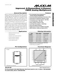
DAC8420 Quad 12-Bit Serial Voltage Output DAC
DAC8420 Quad 12-Bit Serial Voltage Output DAC
DAC8420 Quad 12-Bit Serial Voltage Output DAC

You also want an ePaper? Increase the reach of your titles
YUMPU automatically turns print PDFs into web optimized ePapers that Google loves.
<strong><strong>DAC</strong>8420</strong><br />
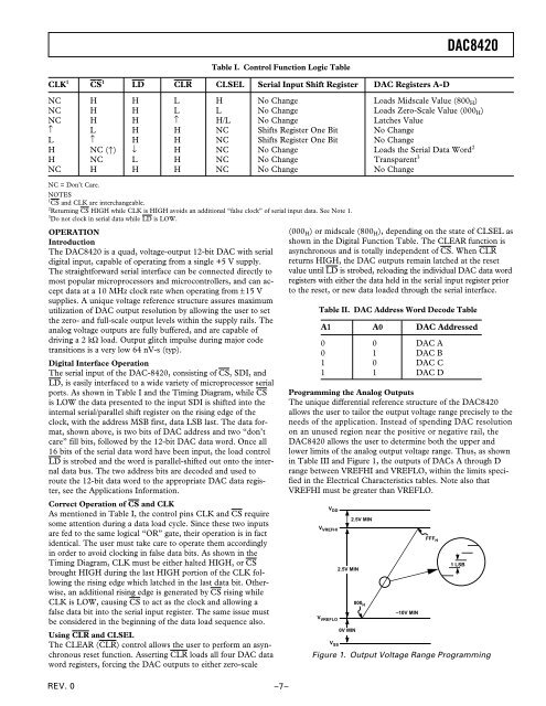
Table I. Control Function Logic Table<br />
CLK 1 CS 1 LD CLR CLSEL <strong>Serial</strong> Input Shift Register <strong>DAC</strong> Registers A-D<br />
NC H H L H No Change Loads Midscale Value (800 H )<br />
NC H H L L No Change Loads Zero-Scale Value (000 H )<br />
NC H H ↑ H/L No Change Latches Value<br />
↑ L H H NC Shifts Register One <strong>Bit</strong> No Change<br />
L ↑ H H NC Shifts Register One <strong>Bit</strong> No Change<br />
H NC (↑) ↓ H NC No Change Loads the <strong>Serial</strong> Data Word 2<br />
H NC L H NC No Change Transparent 3<br />
NC H H H NC No Change No Change<br />
NC = Don’t Care.<br />
NOTES<br />
1 CS and CLK are interchangeable.<br />
2 Returning CS HIGH while CLK is HIGH avoids an additional “false clock” of serial input data. See Note 1.<br />
3 Do not clock in serial data while LD is LOW.<br />
OPERATION<br />
Introduction<br />
The <strong><strong>DAC</strong>8420</strong> is a quad, voltage-output <strong>12</strong>-bit <strong>DAC</strong> with serial<br />
digital input, capable of operating from a single +5 V supply.<br />
The straightforward serial interface can be connected directly to<br />
most popular microprocessors and microcontrollers, and can accept<br />
data at a 10 MHz clock rate when operating from ±15 V<br />
supplies. A unique voltage reference structure assures maximum<br />
utilization of <strong>DAC</strong> output resolution by allowing the user to set<br />
the zero- and full-scale output levels within the supply rails. The<br />
analog voltage outputs are fully buffered, and are capable of<br />
driving a 2 kΩ load. <strong>Output</strong> glitch impulse during major code<br />
transitions is a very low 64 nV-s (typ).<br />
Digital Interface Operation<br />
The serial input of the <strong>DAC</strong>-8420, consisting of CS, SDI, and<br />
LD, is easily interfaced to a wide variety of microprocessor serial<br />
ports. As shown in Table I and the Timing Diagram, while CS<br />
is LOW the data presented to the input SDI is shifted into the<br />
internal serial/parallel shift register on the rising edge of the<br />
clock, with the address MSB first, data LSB last. The data format,<br />
shown above, is two bits of <strong>DAC</strong> address and two “don’t<br />
care” fill bits, followed by the <strong>12</strong>-bit <strong>DAC</strong> data word. Once all<br />
16 bits of the serial data word have been input, the load control<br />
LD is strobed and the word is parallel-shifted out onto the internal<br />
data bus. The two address bits are decoded and used to<br />
route the <strong>12</strong>-bit data word to the appropriate <strong>DAC</strong> data register,<br />
see the Applications Information.<br />
Correct Operation of CS and CLK<br />
As mentioned in Table I, the control pins CLK and CS require<br />
some attention during a data load cycle. Since these two inputs<br />
are fed to the same logical “OR” gate, their operation is in fact<br />
identical. The user must take care to operate them accordingly<br />
in order to avoid clocking in false data bits. As shown in the<br />
Timing Diagram, CLK must be either halted HIGH, or CS<br />
brought HIGH during the last HIGH portion of the CLK following<br />
the rising edge which latched in the last data bit. Otherwise,<br />
an additional rising edge is generated by CS rising while<br />
CLK is LOW, causing CS to act as the clock and allowing a<br />
false data bit into the serial input register. The same issue must<br />
be considered in the beginning of the data load sequence also.<br />
Using CLR and CLSEL<br />
The CLEAR (CLR) control allows the user to perform an asynchronous<br />
reset function. Asserting CLR loads all four <strong>DAC</strong> data<br />
word registers, forcing the <strong>DAC</strong> outputs to either zero-scale<br />
(000 H ) or midscale (800 H ), depending on the state of CLSEL as<br />
shown in the Digital Function Table. The CLEAR function is<br />
asynchronous and is totally independent of CS. When CLR<br />
returns HIGH, the <strong>DAC</strong> outputs remain latched at the reset<br />
value until LD is strobed, reloading the individual <strong>DAC</strong> data word<br />
registers with either the data held in the serial input register prior<br />
to the reset, or new data loaded through the serial interface.<br />
Table II. <strong>DAC</strong> Address Word Decode Table<br />
A1 A0 <strong>DAC</strong> Addressed<br />
0 0 <strong>DAC</strong> A<br />
0 1 <strong>DAC</strong> B<br />
1 0 <strong>DAC</strong> C<br />
1 1 <strong>DAC</strong> D<br />
Programming the Analog <strong>Output</strong>s<br />
The unique differential reference structure of the <strong><strong>DAC</strong>8420</strong><br />
allows the user to tailor the output voltage range precisely to the<br />
needs of the application. Instead of spending <strong>DAC</strong> resolution<br />
on an unused region near the positive or negative rail, the<br />
<strong><strong>DAC</strong>8420</strong> allows the user to determine both the upper and<br />
lower limits of the analog output voltage range. Thus, as shown<br />
in Table III and Figure 1, the outputs of <strong>DAC</strong>s A through D<br />
range between VREFHI and VREFLO, within the limits specified<br />
in the Electrical Characteristics tables. Note also that<br />
VREFHI must be greater than VREFLO.<br />
V DD<br />
V VREFHI<br />
V VREFLO<br />
V SS<br />
2.5V MIN<br />
0V MIN<br />
2.5V MIN<br />
000 H<br />
–10V MIN<br />
FFF H<br />
1 LSB<br />
Figure 1. <strong>Output</strong> <strong>Voltage</strong> Range Programming<br />
REV. 0 –7–