Template for Tec Docs - Inova Semiconductors
Template for Tec Docs - Inova Semiconductors
Template for Tec Docs - Inova Semiconductors

You also want an ePaper? Increase the reach of your titles
YUMPU automatically turns print PDFs into web optimized ePapers that Google loves.
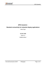
Application Note<br />
AN101 Automotive Usage<br />
APIX – Using the Sideband channels<br />
Order ID: AN_INAP_101<br />
February 2009<br />
Revision 1.3<br />
Abstract<br />
APIX (Automotive PIXel Link) is a high speed serial link <strong>for</strong> transferring Video/Audio data in Cameras and Displays<br />
in Automotive Applications such as Infotainment and Driver Assistance systems. The link supports a<br />
downstream data rate of up to 1 Gbit/s. In addition, APIX features a full duplex, bidirectional sideband channel<br />
over the same or a separate link. This link can be used to implement an independent control channel.<br />
This application note describes in detail how to connect and configure the INAP125T to use the sideband interface.<br />
System Architecture<br />
The APIX Interface devices provide an uni-directional parallel TTL video interface and a bi-directional sideband<br />
interface (Figure 1). The serial interconnection between transmitter and receiver device comprises a high<br />
speed differential down link and if required a lower speed differential up link.<br />
Figure 1: APIX parallel and serial interconnections<br />
Alternatively the upstream link can also be established via common mode signaling on the down link twisted<br />
pair. This allows an implementation of the entire link with only two wires, however impacting the EMI robustness<br />
of link, since the upstream sideband data is transferred as common mode signal.<br />
For automotive applications it is recommended to use the dedicated CML data link in upstream direction.<br />
February 19, 2009 Revision 1.3 AN_INAP_101 Page 1 of 11
Application Note<br />
Introduction to the Side band Interface<br />
Common Serializer / Deserializer (SERDES) devices are designed and optimized to convert parallel data into<br />
a high speed serial stream, which is transmitted from a TX device to a RX device using differential signalling.<br />
This serial transmission allows higher speed and longer range with the benefit of very low EMI over a single<br />
pair of cables. However, the link is optimized <strong>for</strong> uni-directional high speed data as required in video streaming<br />
applications.<br />
Especially in automotive applications, the requirements <strong>for</strong> higher integration and reuse of existing media gets<br />
more and more important. Besides video data, systems like Rear Seat entertainments or remote cameras require<br />
power supply and control data to be exchanged with the main unit with a minimum amount of cables.<br />
To address these requirements, the APIX technology features up to 2 full duplex, bidirectional sideband channels<br />
on the same or a separate pair of cables. This link offers full flexibility from the transmission of simple status<br />
flags, directly sampling interfaces like UART or SPI, up to complex protocols like AShell (see [2]). The AC<br />
coupled physical layer allows to induce the DC power supply <strong>for</strong> the remote system like cameras onto the APIX<br />
data lines.<br />
Compared to other SERDES implementations, APIX offers the advantage to be able to send sideband data<br />
independent to the video interface. The video interface clock often is used as main reference clock <strong>for</strong> transmitter<br />
and the high speed serial link. This architecture <strong>for</strong>ces the pixel clock to be active <strong>for</strong> sending sideband<br />
data or to keep the link alive. This gets especially critical <strong>for</strong> applications requiring upstream capabilities with<br />
random data like keyboard or remote control.<br />
Within the APIX devices the high speed serial link is „decoupled” from the video data interface by using a separate<br />
system clock <strong>for</strong> the serial link (see [3]). The link powers up and synchronizes independently to the pixel<br />
clock, there<strong>for</strong>e there‘s no need <strong>for</strong> special video interface handling to drive the sideband.<br />
The APIX architecture supports full duplex operation by implementing the upstream sideband channel either<br />
embedded as common mode signaling or on a dedicated cable.<br />
Sideband interface<br />
The sideband interface on both the transmitter and receiver devices consists of the data pins and the corresponding<br />
clock outputs. The sideband data inputs are sampled asynchronously to the application using an internally<br />
generated reference clock and are transmitted with low latency. At the sideband data outputs the data<br />
are provided in sync to the sampling clock.<br />
For the APIX link, the downstream sideband channel is defined as serial stream from the transmitter to the receiver,<br />
the upstream sideband channel as serial stream from receiver to the transmitter.<br />
The Sideband data are available or have to be supplied to the following pins<br />
• SBDOWN_DATA[1:0] 1 :<br />
– Data input (TX) or data output (RX) of the downstream data<br />
• SBDOWN_CLK:<br />
– Clock output at RX, synchronous clock <strong>for</strong> SBDOWN_DATA<br />
• SBUP_DATA[1:0] 1 :<br />
– Data output (TX) or data input (RX) of the upstream data<br />
• SBUP_CLK:<br />
– Clock output at TX, synchronous clock <strong>for</strong> SBUP_DATA<br />
Please see also Figure 2 and Figure 3 <strong>for</strong> the sideband data flow in both directions.<br />
1. The number of available data pins depends on the package. Please check [1] <strong>for</strong> available package options.<br />
February 19, 2009 Revision 1.3 AN_INAP_101 Page 2 of 11
Application Note<br />
Figure 2: Downstream sideband channel pins<br />
Figure 3: Upstream sideband channel pins<br />
Downstream and upstream link have different clocking and sampling schemes, which are described in the following<br />
sections.<br />
February 19, 2009 Revision 1.3 AN_INAP_101 Page 3 of 11
Application Note<br />
Downstream<br />
In order to support both video and separate sideband channel, the downstream data path is a combination of<br />
the data sampled at the pixel data interface PX_DATA[23:0] and the sideband data SBDOWN_DATA[1:0]. The<br />
transmission is per<strong>for</strong>med as merged frames of 18bits, which typically hold 16 bits of data and 2 bits of balancing<br />
overhead. The sideband bits are filled in every 4th frame, which guarantees a constant bandwidth.<br />
Figure 4 illustrates the merged transport of sideband and pixel data on the downstream.<br />
Figure 4: Downstream transport including sideband data (simplified)<br />
The maximum gross downstream data rate <strong>for</strong> the APIX link is 1GBit/s. Considering the values <strong>for</strong> payload and<br />
overhead, the sampling rate <strong>for</strong> the downstream sideband pins at 1GBit/s can be calculated to<br />
1GHz / (4 *18) = 13.89 MHz<br />
<strong>for</strong> 500MBit/s mode this results in<br />
500MHz / (4 *18) = 6.94 MHz<br />
This sampling clock is derived as divided clock from the internal system clock at the transmitter devices<br />
INAP125Txx. As the sideband interface is sampled asynchronously, the maximum bandwidth <strong>for</strong> a digital data<br />
stream is slightly lower than the sampling frequency.<br />
Please see Table 1 as summary of the sampling frequency in the different bandwidth modes. The downstream<br />
speed is configured by a configuration vector (see [1]).<br />
Downstream speed<br />
1GBit/s<br />
SBDOWN_DATA[1:0]<br />
Sampling frequency<br />
13.89 MHz<br />
500 MBit/s 6.94 MHz<br />
Table 1: Downstream Sideband bandwidth and sampling frequency<br />
The receiver clock data recovery (CDR) at the receiver devices extracts the clock and data and provides them<br />
at SBDOWN_CLK and SBDOWN_DATA[1:0].<br />
February 19, 2009 Revision 1.3 AN_INAP_101 Page 4 of 11
Application Note<br />
Downstream Jitter and Latency<br />
Due to the asynchronous sampling of the SBDOWN_DATA pins, the data output at the receiver includes a certain<br />
jitter compared to the data sampled at the transmitter. The maximum jitter is defined by the time between<br />
two rising edges of the sampling clock and there<strong>for</strong>e mainly defined by the sampling frequency. Figure 5 illustrates<br />
overall latency between the sampled and received data at SBDOWN_DATA as combination of the jitter<br />
and the transmission delay.<br />
Figure 5: Jitter and transmission delay of the sideband transmission<br />
The transmission delay results from the transmission line, which depends on the cable length and the processing<br />
time of the chip.<br />
The following plots at Figure 6 and Figure 7 show SBDOWN_DATA at the receiver compared to<br />
SBDOWN_DATA input at the transmitter at a cable length of 1 meter and 5 meter. As illustrated in Figure 5,<br />
the transmission delay grows with the cable length, while the jitter stays at a constant rate of about 72ns, which<br />
reflects the 13.89Mhz sampling frequency. In 500Mbit/s mode, the jitter increases to 144ns as the system clock<br />
and the sampling frequency is halved to 6.94MHz. The overall latency increases accordingly.<br />
Please note, that the values below have to be seen as examples and can vary between different cables and<br />
chips. The measurements have been per<strong>for</strong>med using the standard APIX evaluation kit and Leoni Dacar 538<br />
cables.<br />
February 19, 2009 Revision 1.3 AN_INAP_101 Page 5 of 11
Application Note<br />
Channel 2: TX SBDOWN_DATA Input<br />
Channel 3: RX SBDOWN_DATA Output<br />
Bandwidth Mode: 1GBits/s<br />
Bandwidth Mode: 500MBit/s<br />
Figure 6: Transmission Delay and Jitter at a cable length of 1m<br />
Please see Table 2 <strong>for</strong> an overview of maximum jitter and latency of the downstream sideband link at 1m cable<br />
length.<br />
Bandwidth mode<br />
Maximum jitter<br />
Downstream delay<br />
@ 1m (measured)<br />
Maximum Latency<br />
1 GBit/s 72 ns 140 ns 212 ns<br />
500 MBit/s 144 ns 264 ns 408 ns<br />
Table 2: Downstream jitter and latency at a cable length of 1m<br />
February 19, 2009 Revision 1.3 AN_INAP_101 Page 6 of 11
Application Note<br />
Channel 2: TX SBDOWN_DATA Input<br />
Channel 3: RX SBDOWN_DATA Output<br />
Bandwidth Mode: 1GBit/s<br />
Bandwidth Mode: 500MBits/s<br />
Figure 7: Transmission Delay and Jitter at a cable length of 5m<br />
Bandwidth mode<br />
Maximum jitter<br />
Downstream delay<br />
@ 5m (measured)<br />
Maximum Latency<br />
1 GBit/s 72 ns 164 ns 236 ns<br />
500 MBit/s 144 ns 286 ns 430 ns<br />
Table 3: Downstream jitter and latency at a cable length of 5m<br />
February 19, 2009 Revision 1.3 AN_INAP_101 Page 7 of 11
Application Note<br />
Upstream<br />
The APIX link features a flexible upstream link, which is established either<br />
• embedded, via common mode signaling, using the same pair of cables as the downstream.<br />
• dedicated, via differential signaling, using a separate pair of cables.<br />
Both signaling modes do not require any switching mechanism at the driver stage of the differential signals,<br />
which may cause switching noise and there<strong>for</strong>e EMI issues. In addition, both modes allow full duplex operation<br />
of upstream and downstream.<br />
However, common mode signaling uses the shield of the cable <strong>for</strong> the back-current. There<strong>for</strong>e the benefit of<br />
using a single pair of cables may not be applicable <strong>for</strong> the stringent EMI requirements of automotive applications.<br />
Using the dedicated upstream functionality would be recommended <strong>for</strong> these applications.<br />
Upstream data are sampled and provided at SBUP_DATA[1:0]. Similar to the downstream sideband, the pins<br />
are sampled asynchronously by an internally generated clock. The upstream data stream is handled independently<br />
to the downstream speed, which provides higher flexibility on sampling frequency and bandwidth.<br />
The upstream data are sent in frames of 3 bit, consisting of 2 bits of data and 1 bit overhead. The upstream<br />
serial clock can be configured to a maximum value of 62.5 MHz, which leads to a maximum bit clock per channel<br />
of<br />
(62.5 MHz / 3 bit) / 2 channels = 10.41 MHz<br />
The selection <strong>for</strong> the transmission mode and the sampling frequency needs to be per<strong>for</strong>med as parameter in<br />
the configuration vector (see [1]). The upstream link requires the configuration to be done at both the transmitter<br />
and the receiver devices. The main bandwidth mode configuration defines the general system clock, thus<br />
also influences the upstream sampling frequency.<br />
Please see Table 4 as summary <strong>for</strong> all different configurations possible <strong>for</strong> the upstream link.<br />
Configuration<br />
Dedicated upstream<br />
Embedded upstream<br />
Bandwidth Mode<br />
Upstream Link serial clock<br />
1GBit/s a<br />
Configuration Options<br />
Enable / Disable<br />
Enable / Disable<br />
1 GBit/s / 500 MBit/s<br />
Upstream serial clock / Sampling freq.<br />
62.5 MHz / 10.41 MHz<br />
41.7 MHz / 6.94 MHz<br />
31.25 MHz / 5.21 MHz<br />
Upstream Link serial clock<br />
500 MBit/s a Upstream serial clock / Sampling freq.<br />
62.5 MHz / 10.41 MHz<br />
31.25 MHz / 5.21 MHz<br />
20.83 MHz / 3.47 MHz<br />
a.defined by bandwidth mode configuration<br />
Table 4: Upstream configuration<br />
Upstream data and clock are provided at the transmitter at SBUP_DATA[1:0] and SBUP_CLK.<br />
February 19, 2009 Revision 1.3 AN_INAP_101 Page 8 of 11
Application Note<br />
Upstream Jitter and Latency<br />
Similar to the downstream link, the upstream sideband transmission link introduces a certain latency and jitter<br />
onto the data path. The upstream data path can be configured to different sampling speeds and settings. Since<br />
the upstream uses its own sampling and framing scheme, the transmission latency and jitter are not affected<br />
by the bandwidth mode selection (1GBit/s, 500MBit/s) directly. However, it is affected by the sampling frequency,<br />
which is defined by the upstream serial line clock setting.<br />
Figure 8 shows the influence of the cable length on the upstream sideband.<br />
Channel 3: RX SBUP_DATA Input<br />
Channel 2: TX SBUP_DATA Output<br />
Sampling frequency: 62.5MHz<br />
Cable Length: 1 meter<br />
Cable Length: 5 meter<br />
Figure 8: Upstream Transmission Delay and Jitter<br />
The maximum upstream jitter again depends on the sample frequency and is specified as listed in Table 5.<br />
Upstream serial line clock Sample frequency Maximum jitter<br />
62.50 MHz 10.41 MHz 104 ns<br />
41.67 MHz 6.94 MHz 152 ns<br />
31.25 MHz 5.21 MHz 200 ns<br />
20.83 MHz 3.47 MHz 304 ns<br />
Table 5: Maximum upstream jitter <strong>for</strong> the different serial line clocks<br />
February 19, 2009 Revision 1.3 AN_INAP_101 Page 9 of 11
Application Note<br />
Table 6 and Table 7 show the latency calculated from the jitter and the measurements at the test board. The<br />
measurements have shown a transmission delay of the cable of approximately 5.5 ns per meter <strong>for</strong> this setup.<br />
Upstream serial<br />
line clock<br />
Maximum jitter<br />
Transmission Delay<br />
measured @ 1m<br />
Maximum Latency<br />
62.50 MHz 104 ns 134 ns 238 ns<br />
31.25 MHz 200 ns 304 ns 504 ns<br />
20.83 MHz 304 ns 432 ns 706 ns<br />
Table 6: Upstream Latency at 500Mbit/s<br />
Upstream serial<br />
line clock<br />
Maximum jitter<br />
Transmission Delay<br />
measured @ 1m<br />
Maximum Latency<br />
62.50 MHz 104 ns 126 ns 230 ns<br />
41.67 MHz 152 ns 230 ns 382 ns<br />
31.25 MHz 200 ns 292 ns 492 ns<br />
Table 7: Upstream Latency at 1Gbit/s<br />
February 19, 2009 Revision 1.3 AN_INAP_101 Page 10 of 11
Application Note<br />
Bibliography<br />
[1] – INAP125T and INAP125R Datasheets, Digital Automotive Pixel Link Datasheets, <strong>Inova</strong> <strong>Semiconductors</strong><br />
[2] – AShell <strong>Tec</strong>hnical Documentation, <strong>Inova</strong> <strong>Semiconductors</strong><br />
[3] – AN 100, Video Interface Configuration Application Note, <strong>Inova</strong> <strong>Semiconductors</strong><br />
<strong>Inova</strong> <strong>Semiconductors</strong> GmbH<br />
Grafinger Str. 26<br />
D-81671 Munich / Germany<br />
Phone: +49 (0)89 / 45 74 75 - 60<br />
Fax: +49 (0)89 / 45 74 75 - 88<br />
Email: info@inova-semiconductors.de<br />
URL: http://www.inova-semiconductors.com<br />
is a registered trademark of <strong>Inova</strong> <strong>Semiconductors</strong> GmbH<br />
All other trademarks or registered trademarks are the property of their respective holders.<br />
<strong>Inova</strong> <strong>Semiconductors</strong> GmbH does not assume any liability arising out of the applications or use of the product described herein; nor does<br />
it convey any license under its patents, copyright rights or any rights of others.<br />
<strong>Inova</strong> <strong>Semiconductors</strong> products are not designed, intended or authorized <strong>for</strong> use as components in systems to support or sustain life, or<br />
<strong>for</strong> any other application in which the failure of the product could create a situation where personal injury or death may occur. The in<strong>for</strong>mation<br />
contained in this document is believed to be current and accurate as of the publication date. <strong>Inova</strong> <strong>Semiconductors</strong> GmbH reserves<br />
the right to make changes at any time in order to improve reliability, function or per<strong>for</strong>mance to supply the best product possible.<br />
<strong>Inova</strong> <strong>Semiconductors</strong> GmbH assumes no obligation to correct any errors contained herein or to advise any user of this text of any correction<br />
if such be made.<br />
© <strong>Inova</strong> <strong>Semiconductors</strong> 2008<br />
February 19, 2009 Revision 1.3 AN_INAP_101 Page 11 of 11