Enhanced RS-232 Line Drivers and Receivers
Enhanced RS-232 Line Drivers and Receivers
Enhanced RS-232 Line Drivers and Receivers

You also want an ePaper? Increase the reach of your titles
YUMPU automatically turns print PDFs into web optimized ePapers that Google loves.
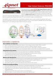
FEATURES…<br />
The SP<strong>232</strong>A/233A/310A/312A devices are a<br />
family of line driver <strong>and</strong> receiver pairs that meet<br />
the specifications of <strong>RS</strong>-<strong>232</strong> <strong>and</strong> V.28 serial<br />
protocols. The ESD tolerance has been improved<br />
on these devices to over ±2KV for the<br />
Human Body Model. These devices are pin-topin<br />
compatible with popular industry st<strong>and</strong>ards.<br />
The SP<strong>232</strong>A/233A/310A/312A devices<br />
feature10V/µs slew rate, 120Kbps data rate under<br />
load, 0.1µF charge pump capacitors, overall<br />
ruggedness for commercial applications, <strong>and</strong><br />
increased drive current for longer <strong>and</strong> more<br />
flexible cable configurations. This family also<br />
features Sipex's BiCMOS design allowing low<br />
power operation without sacrificing performance.<br />
The SP<strong>232</strong>A/233A/310A/312A devices have<br />
internal charge pump voltage converters which<br />
allow them to operate from a single +5V supply.<br />
The charge pumps will operate with polarized or<br />
non-polarized capacitors ranging from 0.1 to 1µF<br />
<strong>and</strong> will generate the ±6V needed for the <strong>RS</strong>-<br />
<strong>232</strong> output levels. Both meet all EIA <strong>RS</strong>-<strong>232</strong>F<br />
<strong>and</strong> ITU V.28 specifications.<br />
The SP310A provides identical features as the<br />
SP<strong>232</strong>A with the addition of a single control<br />
line which simultaneously shuts down the internal<br />
DC/DC converter <strong>and</strong> puts all transmitter<br />
<strong>and</strong> receiver outputs into a high impedance<br />
state. The SP312A is identical to the SP310A<br />
with separate tri-state <strong>and</strong> shutdown control<br />
lines.<br />
THEORY OF OPERATION<br />
The SP<strong>232</strong>A, SP233A, SP310A <strong>and</strong> SP312A<br />
devices are made up of three basic circuit blocks –<br />
1) a driver/transmitter, 2) a receiver <strong>and</strong> 3) a charge<br />
pump. Each block is described below.<br />
Driver/Transmitter<br />
The drivers are inverting transmitters, which accept<br />
TTL or CMOS inputs <strong>and</strong> output the <strong>RS</strong>-<strong>232</strong><br />
signals with an inverted sense relative to the input<br />
logic levels. Typically the <strong>RS</strong>-<strong>232</strong>output voltage<br />
swing is ±6V. Even under worst case loading<br />
conditions of 3kOhms <strong>and</strong> 2500pF, the output is<br />
guaranteed to be ±5V, which is consistent with the<br />
<strong>RS</strong>-<strong>232</strong> st<strong>and</strong>ard specifications. The transmitter<br />
outputs are protected against infinite short-circuits<br />
to ground without degradation in reliability.<br />
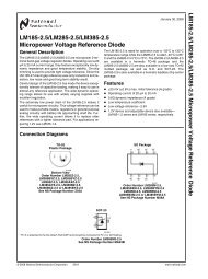
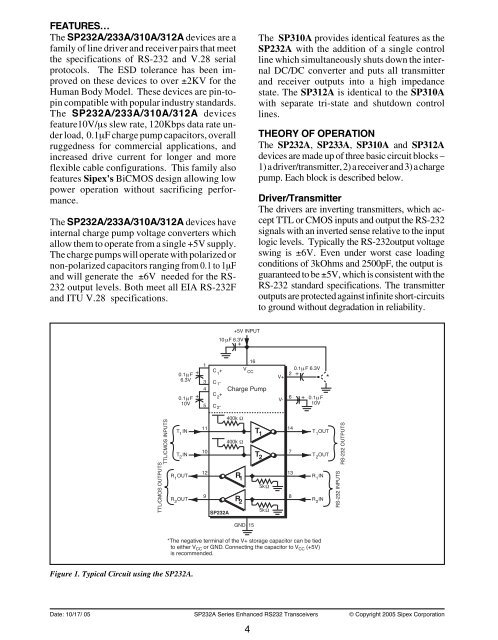
+5V INPUT<br />
10 µ F 6.3V<br />
+<br />
0.1 µ F<br />
6.3V<br />
0.1 µ F<br />
10V<br />
+<br />
+<br />
1<br />
3<br />
4<br />
5<br />
C +<br />
1<br />
C 1-<br />
C +<br />
2<br />
C 2-<br />
16<br />
V CC<br />
V+<br />
Charge Pump<br />
V-<br />
0.1 µ F 6.3V<br />
2<br />
6<br />
+<br />
+<br />
0.1 µ F<br />
10V<br />
*<br />
TTL/CMOS OUTPUTS<br />
TTL/CMOS INPUTS<br />
T IN<br />
1<br />
T IN<br />
2<br />
R OUT<br />
1<br />
R OUT<br />
2<br />
400k Ω<br />
11 14<br />
T 1<br />
400k Ω<br />
10 7<br />
T 2<br />
12 13<br />
R 1<br />
5k Ω<br />
9 8<br />
R 2<br />
SP<strong>232</strong>A<br />
5k Ω<br />
T OUT<br />
1<br />
T OUT<br />
2<br />
R IN<br />
1<br />
R IN<br />
2<br />
<strong>RS</strong>-<strong>232</strong> INPUTS<br />
<strong>RS</strong>-<strong>232</strong> OUTPUTS<br />
GND 15<br />
*The negative terminal of the V+ storage capacitor can be tied<br />
to either V CC or GND. Connecting the capacitor to V CC (+5V)<br />
is recommended.<br />
Figure 1. Typical Circuit using the SP<strong>232</strong>A.<br />
Date: 10/17/ 05 SP<strong>232</strong>A Series <strong>Enhanced</strong> <strong>RS</strong><strong>232</strong> Transceivers © Copyright 2005 Sipex Corporation<br />
4