Enhanced RS-232 Line Drivers and Receivers
Enhanced RS-232 Line Drivers and Receivers
Enhanced RS-232 Line Drivers and Receivers

Create successful ePaper yourself
Turn your PDF publications into a flip-book with our unique Google optimized e-Paper software.
®<br />
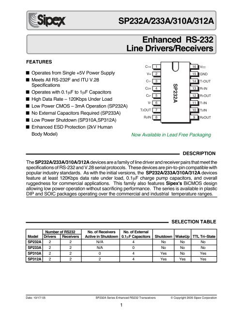
SP<strong>232</strong>A/233A/310A/312A<br />
<strong>Enhanced</strong> <strong>RS</strong>-<strong>232</strong><br />
<strong>Line</strong> <strong>Drivers</strong>/<strong>Receivers</strong><br />
FEATURES<br />
■ Operates from Single +5V Power Supply<br />
■ Meets All <strong>RS</strong>-<strong>232</strong>F <strong>and</strong> ITU V.28<br />
Specifications<br />
■ Operates with 0.1µF to 1µF Capacitors<br />
■ High Data Rate – 120Kbps Under Load<br />
■ Low Power CMOS – 3mA Operation (SP<strong>232</strong>A)<br />
■ No External Capacitors Required (SP233A)<br />
■ Low Power Shutdown (SP310A,SP312A)<br />
■ <strong>Enhanced</strong> ESD Protection (2kV Human<br />
Body Model)<br />
C1+ 1<br />
V+ 2<br />
C1- 3<br />
C2+ 4<br />
C2- 5<br />
V- 6<br />
T2OUT 7<br />
R2IN 8<br />
SP<strong>232</strong>A<br />
16<br />
15<br />
14<br />
13<br />
12<br />
11<br />
10<br />
9<br />
VCC<br />
GND<br />
T1OUT<br />
R1IN<br />
R1OUT<br />
T1IN<br />
T2IN<br />
R2OUT<br />
Now Available in Lead Free Packaging<br />
DESCRIPTION<br />
The SP<strong>232</strong>A/233A/310A/312A devices are a family of line driver <strong>and</strong> receiver pairs that meet the<br />
specifications of <strong>RS</strong>-<strong>232</strong> <strong>and</strong> V.28 serial protocols. These devices are pin-to-pin compatible with<br />
popular industry st<strong>and</strong>ards. As with the initial versions, the SP<strong>232</strong>A/233A/310A/312A devices<br />
feature at least 120Kbps data rate under load, 0.1µF charge pump capacitors, <strong>and</strong> overall<br />
ruggedness for commercial applications. This family also features Sipex's BiCMOS design<br />
allowing low power operation without sacrificing performance. The series is available in plastic<br />
DIP <strong>and</strong> SOIC packages operating over the commercial <strong>and</strong> industrial temperature ranges.<br />
SELECTION TABLE<br />
Number of <strong>RS</strong><strong>232</strong> No. of <strong>Receivers</strong> No. of External<br />
Model <strong>Drivers</strong> <strong>Receivers</strong> Active in Shutdown 0.1µF Capacitors Shutdown WakeUp TTL Tri–State<br />
SP<strong>232</strong>A 2 2 N//A 4 No No No<br />
SP233A 2 2 N/A 0 No No No<br />
SP310A 2 2 0 4 Yes No Yes<br />
SP312A 2 2 2 4 Yes Yes Yes<br />
Date: 10/17/ 05 SP<strong>232</strong>A Series <strong>Enhanced</strong> <strong>RS</strong><strong>232</strong> Transceivers © Copyright 2005 Sipex Corporation<br />
1
This is a stress rating only <strong>and</strong> functional operation of the device at<br />
these or any other conditions above those indicated in the operation<br />
sections of this specification is not implied. Exposure to absolute<br />
maximum rating conditions for extended periods of time may affect<br />
reliability.<br />
V cc<br />
................................................................................................................................................................. +6V<br />
V + .................................................................................................................... (Vcc-0.3V) to +11.0V<br />
V - ............................................................................................................................................................ -11.0V<br />
Input Voltages<br />
T IN<br />
......................................................................................................................... -0.3 to (Vcc +0.3V)<br />
R IN<br />
............................................................................................................................................................ ±30V<br />
V CC<br />
=+5V±10%; 0.1µF charge pump capacitors; T MIN<br />
to T MAX<br />
unless otherwise noted.<br />
ABSOLUTE MAXIMUM RATINGS<br />
Output Voltages<br />
T OUT<br />
.................................................................................................... (V+, +0.3V) to (V-, -0.3V)<br />
R OUT<br />
................................................................................................................ -0.3V to (Vcc +0.3V)<br />
Short Circuit Duration<br />
T OUT<br />
......................................................................................................................................... Continuous<br />
Plastic DIP .......................................................................... 375mW<br />
(derate 7mW/°C above +70°C)<br />
Small Outline ...................................................................... 375mW<br />
(derate 7mW/°C above +70°C)<br />
ELECTRICAL CHARACTERISTICS<br />
PARAMETE<strong>RS</strong> MIN. TYP. MAX. UNITS CONDITIONS<br />
TTL INPUT<br />
Logic Threshold<br />
LOW 0.8 Volts T IN<br />
; EN, SD<br />
HIGH 2.0 Volts T IN<br />
; EN, SD<br />
Logic Pull-Up Current 15 200 µA T IN<br />
= ZeroV<br />
TTL OUTPUT<br />
TTL/CMOS Output<br />
Voltage, Low 0.4 Volts<br />
I OUT<br />
= 3.2mA; Vcc = +5V<br />
I<br />
Voltage, High 3.5 Volts<br />
OUT<br />
= -1.0mA<br />
Leakage Current; T A<br />
= +25° 0.05 ±10 µA EN = V CC<br />
, ZeroV≤V OUT<br />
≤V CC<br />
SP310A <strong>and</strong> SP312A only<br />
<strong>RS</strong>-<strong>232</strong> OUTPUT<br />
Output Voltage Swing ±5 ±6 Volts All transmitter outputs loaded<br />
with 3kΩ to Ground<br />
Output Resistance 300 Ohms V CC<br />
= ZeroV; V OUT<br />
= ±2V<br />
Output Short Circuit Current ±18 mA Infinite duration<br />
Maximum Data Rate 120 240 Kbps C L<br />
= 2500pF, R L<br />
= 3kΩ<br />
<strong>RS</strong>-<strong>232</strong> INPUT<br />
Voltage Range -30 +30 Volts<br />
Voltage Threshold<br />
LOW 0.8 1.2 Volts V CC<br />
= 5V, T A<br />
= +25°C<br />
HIGH 1.7 2.4 Volts V CC<br />
= 5V, T A<br />
= +25°C<br />
Hysteresis 0.2 0.5 1.0 Volts V CC<br />
= 5V, T A<br />
= +25°C<br />
Resistance 3 5 7 kΩ T A<br />
= +25°C, -15V ≤ V IN<br />
≤ +15V<br />
DYNAMIC CHARACTERISTICS<br />
Driver Propagation Delay 1.5 3.0 µs TTL to <strong>RS</strong>-<strong>232</strong>; C L<br />
= 50pF<br />
Receiver Propagation Delay 0.1 1.0 µs <strong>RS</strong>-<strong>232</strong> to TTL<br />
Instantaneous Slew Rate 30 V/µs C L<br />
= 10pF, R L<br />
= 3-7kΩ;<br />
T A<br />
=+25°C<br />
Transition Region Slew Rate 10 V/µs C L<br />
= 2500pF, R L<br />
= 3kΩ;<br />
measured from +3V to -3V<br />
or -3V to +3V<br />
Output Enable Time 400 ns SP310A <strong>and</strong> SP312A only<br />
Output Disable Time 250 ns SP310A <strong>and</strong> SP312A only<br />
POWER REQUIREMENTS<br />
V CC<br />
Power Supply Current<br />
SP<strong>232</strong>A 3 5 mA No load, T A<br />
= +25°C; V CC<br />
= 5V<br />
SP233A, SP310A, SP312A 10 15 mA No load, T A<br />
= +25°C; V CC<br />
= 5V<br />
V CC<br />
Supply Current,Loaded<br />
SP<strong>232</strong>A 15 mA All transmitters R L<br />
= 3kΩ;<br />
T A = +25°C<br />
SP233A, SP310A, SP312A 25 mA All transmitters R L<br />
= 3kΩ;<br />
T A<br />
= +25°C<br />
Shutdown Supply Current<br />
SP310A,SP312A 1 10 µA V CC<br />
= 5V, T A<br />
= +25°C<br />
Date: 10/17/ 05 SP<strong>232</strong>A Series <strong>Enhanced</strong> <strong>RS</strong><strong>232</strong> Transceivers © Copyright 2005 Sipex Corporation<br />
2
Not 100% tested.<br />
PERFORMANCE CURVES<br />
V– Voltage (Volts)<br />
-11<br />
-10<br />
-9<br />
-8<br />
VCC = 6V<br />
-7<br />
VCC = 5V<br />
-6<br />
VCC = 4V<br />
-5<br />
-4<br />
-3<br />
0 2 4 6 8 10 12 14<br />
Load Current (mA)<br />
V+ (Volts)<br />
12<br />
10<br />
VCC = 6V<br />
VCC = 5V<br />
8<br />
VCC = 4V<br />
6<br />
4<br />
2<br />
0<br />
0 5 10 15 20 25 30 35 40<br />
Load Current (mA)<br />
ICC (mA)<br />
30<br />
25<br />
VCC = 6V<br />
20<br />
15<br />
VCC = 5V<br />
10<br />
VCC = 4V<br />
5<br />
VCC = 3V<br />
0<br />
-55 -40 0 25 70 85 125<br />
Temperature (°C)<br />
VOH (Volts)<br />
9.0<br />
8.5<br />
8.0<br />
7.5<br />
7.0<br />
Load current = 0mA<br />
TA = 25°C<br />
6.5<br />
6.0<br />
5.5<br />
5.0<br />
4.5 4.75 5.0 5.25 5.5<br />
VCC (Volts)<br />
PINOUTS<br />
C1+<br />
V+<br />
C1-<br />
C2+<br />
C2-<br />
V-<br />
T2OUT<br />
R2IN<br />
1<br />
2<br />
3<br />
4<br />
5<br />
6<br />
7<br />
8<br />
SP<strong>232</strong>A<br />
16<br />
15<br />
14<br />
13<br />
12<br />
11<br />
10<br />
9<br />
VCC<br />
GND<br />
T1OUT<br />
R1IN<br />
R1OUT<br />
T1IN<br />
T2IN<br />
R2OUT<br />
T2IN<br />
T1IN<br />
R1OUT<br />
R1IN<br />
T1OUT<br />
GND<br />
VCC<br />
V+ DNC<br />
GND<br />
Conn to 17<br />
1<br />
2<br />
3<br />
4<br />
5<br />
6<br />
7<br />
8<br />
9<br />
10<br />
SP233ACT/AET<br />
20<br />
19<br />
18<br />
17<br />
16<br />
15<br />
14<br />
13<br />
12<br />
11<br />
R2OUT<br />
R2IN<br />
T2OUT<br />
Conn to 10<br />
Conn to 11<br />
Conn to 12<br />
C1- DNC<br />
C1+ DNC<br />
Conn to 15<br />
Conn to 16<br />
20-PIN SOIC<br />
See Figure 2 for<br />
Pin Connections<br />
T 2IN<br />
T 1IN<br />
1<br />
2<br />
20<br />
19<br />
R OUT<br />
2<br />
R 2IN<br />
NC *<br />
C1+<br />
1<br />
2<br />
18<br />
17<br />
ON/OFF<br />
VCC<br />
EN *<br />
C1+<br />
1<br />
2<br />
18<br />
17<br />
SHUTDOWN<br />
VCC<br />
R 1OUT<br />
R 1IN<br />
T 1 OUT<br />
GND<br />
VCC<br />
C 1+<br />
GND<br />
3<br />
4<br />
5<br />
6<br />
7<br />
8<br />
9<br />
SP233ACP/AEP<br />
18<br />
17<br />
16<br />
15<br />
14<br />
13<br />
12<br />
T 2OUT<br />
V-<br />
C 2 -<br />
C 2+<br />
V+<br />
C 1 -<br />
V-<br />
T2OUT<br />
R2IN<br />
3<br />
4<br />
5<br />
6<br />
7<br />
8<br />
9<br />
SP310A<br />
16<br />
15<br />
14<br />
13<br />
12<br />
11<br />
10<br />
GND<br />
T1OUT<br />
R1IN<br />
R1OUT<br />
T1IN<br />
T2IN<br />
R2OUT<br />
V+<br />
C1-<br />
C2+<br />
C2-<br />
V-<br />
V+<br />
C1-<br />
C2+<br />
C2-<br />
V-<br />
T2OUT<br />
R2IN<br />
3<br />
4<br />
5<br />
6<br />
7<br />
8<br />
9<br />
SP312A<br />
16<br />
15<br />
14<br />
13<br />
12<br />
11<br />
10<br />
GND<br />
T1OUT<br />
R1IN<br />
R1OUT<br />
T1IN<br />
T2IN<br />
R2OUT<br />
C 2-<br />
10<br />
11<br />
C 2 +<br />
20-PIN PLASTIC DIP<br />
* N.C. for SP310E_A, EN for SP312E_A<br />
Date: 10/17/ 05 SP<strong>232</strong>A Series <strong>Enhanced</strong> <strong>RS</strong><strong>232</strong> Transceivers © Copyright 2005 Sipex Corporation<br />
3
FEATURES…<br />
The SP<strong>232</strong>A/233A/310A/312A devices are a<br />
family of line driver <strong>and</strong> receiver pairs that meet<br />
the specifications of <strong>RS</strong>-<strong>232</strong> <strong>and</strong> V.28 serial<br />
protocols. The ESD tolerance has been improved<br />
on these devices to over ±2KV for the<br />
Human Body Model. These devices are pin-topin<br />
compatible with popular industry st<strong>and</strong>ards.<br />
The SP<strong>232</strong>A/233A/310A/312A devices<br />
feature10V/µs slew rate, 120Kbps data rate under<br />
load, 0.1µF charge pump capacitors, overall<br />
ruggedness for commercial applications, <strong>and</strong><br />
increased drive current for longer <strong>and</strong> more<br />
flexible cable configurations. This family also<br />
features Sipex's BiCMOS design allowing low<br />
power operation without sacrificing performance.<br />
The SP<strong>232</strong>A/233A/310A/312A devices have<br />
internal charge pump voltage converters which<br />
allow them to operate from a single +5V supply.<br />
The charge pumps will operate with polarized or<br />
non-polarized capacitors ranging from 0.1 to 1µF<br />
<strong>and</strong> will generate the ±6V needed for the <strong>RS</strong>-<br />
<strong>232</strong> output levels. Both meet all EIA <strong>RS</strong>-<strong>232</strong>F<br />
<strong>and</strong> ITU V.28 specifications.<br />
The SP310A provides identical features as the<br />
SP<strong>232</strong>A with the addition of a single control<br />
line which simultaneously shuts down the internal<br />
DC/DC converter <strong>and</strong> puts all transmitter<br />
<strong>and</strong> receiver outputs into a high impedance<br />
state. The SP312A is identical to the SP310A<br />
with separate tri-state <strong>and</strong> shutdown control<br />
lines.<br />
THEORY OF OPERATION<br />
The SP<strong>232</strong>A, SP233A, SP310A <strong>and</strong> SP312A<br />
devices are made up of three basic circuit blocks –<br />
1) a driver/transmitter, 2) a receiver <strong>and</strong> 3) a charge<br />
pump. Each block is described below.<br />
Driver/Transmitter<br />
The drivers are inverting transmitters, which accept<br />
TTL or CMOS inputs <strong>and</strong> output the <strong>RS</strong>-<strong>232</strong><br />
signals with an inverted sense relative to the input<br />
logic levels. Typically the <strong>RS</strong>-<strong>232</strong>output voltage<br />
swing is ±6V. Even under worst case loading<br />
conditions of 3kOhms <strong>and</strong> 2500pF, the output is<br />
guaranteed to be ±5V, which is consistent with the<br />
<strong>RS</strong>-<strong>232</strong> st<strong>and</strong>ard specifications. The transmitter<br />
outputs are protected against infinite short-circuits<br />
to ground without degradation in reliability.<br />
+5V INPUT<br />
10 µ F 6.3V<br />
+<br />
0.1 µ F<br />
6.3V<br />
0.1 µ F<br />
10V<br />
+<br />
+<br />
1<br />
3<br />
4<br />
5<br />
C +<br />
1<br />
C 1-<br />
C +<br />
2<br />
C 2-<br />
16<br />
V CC<br />
V+<br />
Charge Pump<br />
V-<br />
0.1 µ F 6.3V<br />
2<br />
6<br />
+<br />
+<br />
0.1 µ F<br />
10V<br />
*<br />
TTL/CMOS OUTPUTS<br />
TTL/CMOS INPUTS<br />
T IN<br />
1<br />
T IN<br />
2<br />
R OUT<br />
1<br />
R OUT<br />
2<br />
400k Ω<br />
11 14<br />
T 1<br />
400k Ω<br />
10 7<br />
T 2<br />
12 13<br />
R 1<br />
5k Ω<br />
9 8<br />
R 2<br />
SP<strong>232</strong>A<br />
5k Ω<br />
T OUT<br />
1<br />
T OUT<br />
2<br />
R IN<br />
1<br />
R IN<br />
2<br />
<strong>RS</strong>-<strong>232</strong> INPUTS<br />
<strong>RS</strong>-<strong>232</strong> OUTPUTS<br />
GND 15<br />
*The negative terminal of the V+ storage capacitor can be tied<br />
to either V CC or GND. Connecting the capacitor to V CC (+5V)<br />
is recommended.<br />
Figure 1. Typical Circuit using the SP<strong>232</strong>A.<br />
Date: 10/17/ 05 SP<strong>232</strong>A Series <strong>Enhanced</strong> <strong>RS</strong><strong>232</strong> Transceivers © Copyright 2005 Sipex Corporation<br />
4
+5V INPUT<br />
+5V INPUT<br />
7<br />
7<br />
V CC<br />
V CC<br />
TTL/CMOS OUTPUTS<br />
TTL/CMOS INPUTS<br />
T IN<br />
1<br />
T IN<br />
2<br />
R OUT<br />
1<br />
R OUT<br />
2<br />
Do not make<br />
connection to<br />
these pins<br />
2 400k Ω<br />
5<br />
T 1<br />
1 400k Ω<br />
18<br />
T 2<br />
3 4<br />
R 1<br />
5kΩ<br />
20 19<br />
R 2<br />
8 C +<br />
5kΩ<br />
1<br />
13<br />
C 1-<br />
C + 11<br />
2<br />
14<br />
V+<br />
C +<br />
15<br />
2<br />
12<br />
10<br />
V-<br />
C 2 -<br />
SP233ACP<br />
16<br />
17 V- GND GND C 2 -<br />
T OUT<br />
1<br />
T OUT<br />
2<br />
R IN<br />
1<br />
R IN<br />
2<br />
<strong>RS</strong>-<strong>232</strong> INPUTS<br />
<strong>RS</strong>-<strong>232</strong> OUTPUTS<br />
Connect on PCB<br />
Pin 11 to Pin 15<br />
Pin 10 to Pin 16<br />
Pin 12 to Pin 17<br />
Both Pins 6 <strong>and</strong> 9 to GND<br />
TTL/CMOS OUTPUTS<br />
TTL/CMOS INPUTS<br />
T IN<br />
1<br />
T IN<br />
2<br />
R OUT<br />
1<br />
R OUT<br />
2<br />
Do not make<br />
connection to<br />
these pins<br />
2 400k Ω<br />
5<br />
T 1<br />
1 400k Ω<br />
18<br />
T 2<br />
3 4<br />
R 1<br />
5k Ω<br />
20 19<br />
R 2<br />
13 C +<br />
5k Ω<br />
1<br />
14<br />
C 1-<br />
C + 12<br />
2<br />
8<br />
V+<br />
C +<br />
15<br />
2<br />
10<br />
11<br />
V-<br />
C 2 -<br />
SP233ACT<br />
17<br />
16<br />
V- GND GND C 2 -<br />
T OUT<br />
1<br />
T OUT<br />
2<br />
R IN<br />
1<br />
R IN<br />
2<br />
<strong>RS</strong>-<strong>232</strong> INPUTS<br />
<strong>RS</strong>-<strong>232</strong> OUTPUTS<br />
Connect on PCB<br />
Pin 12 to Pin 15<br />
Pin 11 to Pin 16<br />
Pin 10 to Pin 17<br />
Both Pins 6 <strong>and</strong> 9 to GND<br />
6<br />
9<br />
6<br />
9<br />
Figure 2. Typical Circuits using the SP233ACP <strong>and</strong> SP233ACT<br />
The instantaneous slew rate of the transmitter<br />
output is internally limited to a maximum of 30V/<br />
µs in order to meet the st<strong>and</strong>ards [EIA <strong>RS</strong>-<strong>232</strong>-F ].<br />
The transition region slew rate of these enhanced<br />
products is typically 10V/µs. The smooth transition<br />
of the loaded output from V OL<br />
to V OH<br />
clearly<br />
meets the monotonicity requirements of the st<strong>and</strong>ard<br />
[EIA <strong>RS</strong>-<strong>232</strong>-F].<br />
<strong>Receivers</strong><br />
The receivers convert <strong>RS</strong>-<strong>232</strong> input signals to<br />
inverted TTL signals. Since the input is usually<br />
from a transmission line, where long cable lengths<br />
<strong>and</strong> system interference can degrade the signal, the<br />
inputs have a typical hysteresis margin of 500mV.<br />
This ensures that the receiver is virtually immune<br />
to noisy transmission lines.<br />
The input thresholds are 0.8V minimum <strong>and</strong> 2.4V<br />
maximum, again well within the ±3V <strong>RS</strong>-<strong>232</strong><br />
requirements. The receiver inputs are also protected<br />
against voltages up to ±25V. Should an<br />
input be left unconnected, a 5KΩ pulldown resistor<br />
to ground will commit the output of the receiver<br />
to a high state.<br />
+5V INPUT<br />
10 µ F 6.3V<br />
+<br />
+5V INPUT<br />
10 µ F 6.3V<br />
+<br />
TTL/CMOS OUTPUTS<br />
TTL/CMOS INPUTS<br />
0.1 µ F +<br />
6.3V<br />
0.1 µ F +<br />
16V<br />
T IN<br />
1<br />
T IN<br />
2<br />
R OUT<br />
1<br />
R OUT<br />
2<br />
2<br />
4<br />
5<br />
6<br />
C +<br />
1<br />
C 1-<br />
C +<br />
2<br />
C 2-<br />
400k Ω<br />
12 15<br />
T 1<br />
400k Ω<br />
11 8<br />
T 2<br />
13 14<br />
R 1<br />
10 9<br />
R 2<br />
GND<br />
17<br />
V CC<br />
V+<br />
Charge Pump<br />
SP310A<br />
16<br />
0.1 µF<br />
10V<br />
3 +<br />
T OUT<br />
1<br />
T OUT<br />
2<br />
Figure 3. Typical Circuits using the SP310A <strong>and</strong> SP312A<br />
5k Ω<br />
5k Ω<br />
V-<br />
7<br />
18<br />
+<br />
R IN<br />
1<br />
R IN<br />
2<br />
*<br />
0.1 µF<br />
10V<br />
ON/OFF<br />
*The negative terminal of the V+ storage capacitor can be tied<br />
to either V CC or GND. Connecting the capacitor to V CC (+5V)<br />
is recommended.<br />
<strong>RS</strong>-<strong>232</strong> INPUTS<br />
<strong>RS</strong>-<strong>232</strong> OUTPUTS<br />
TTL/CMOS OUTPUTS<br />
TTL/CMOS INPUTS<br />
0.1 µ F +<br />
6.3V<br />
T IN<br />
1<br />
T IN<br />
2<br />
R OUT<br />
1<br />
R OUT<br />
2<br />
2<br />
4<br />
5<br />
0.1 µ F +<br />
16V 6<br />
EN<br />
C +<br />
1<br />
C 1-<br />
400k Ω<br />
12 15<br />
T 1<br />
400k Ω<br />
11 8<br />
T 2<br />
13 14<br />
R 1<br />
5kΩ<br />
10 9<br />
R 2<br />
1<br />
C +<br />
2<br />
C 2-<br />
GND<br />
17<br />
V CC<br />
V+<br />
Charge Pump<br />
5kΩ<br />
SP312A<br />
16<br />
V-<br />
0.1 µ F<br />
10V<br />
3 +<br />
7<br />
18<br />
+<br />
0.1 µ F<br />
10V<br />
T OUT<br />
1<br />
T OUT<br />
2<br />
R IN<br />
1<br />
R IN<br />
2<br />
*The negative terminal of the V+ storage capacitor can be tied<br />
to either V CC or GND. Connecting the capacitor to V CC (+5V)<br />
is recommended.<br />
*<br />
<strong>RS</strong>-<strong>232</strong> INPUTS<br />
<strong>RS</strong>-<strong>232</strong> OUTPUTS<br />
SHUTDOWN<br />
Date: 10/17/ 05 SP<strong>232</strong>A Series <strong>Enhanced</strong> <strong>RS</strong><strong>232</strong> Transceivers © Copyright 2005 Sipex Corporation<br />
5
V CC = +5V<br />
+Vcc C 4<br />
+ –<br />
+ +<br />
C 1 C<br />
–<br />
2<br />
–<br />
– +<br />
–Vcc<br />
–Vcc<br />
C 3<br />
V DD Storage Capacitor (V+)<br />
V SS Storage Capacitor (V-)<br />
Figure 4. Charge Pump — Phase 1<br />
In actual system applications, it is quite possible<br />
for signals to be applied to the receiver inputs<br />
before power is applied to the receiver circuitry.<br />
This occurs, for example, when a PC user attempts<br />
to print, only to realize the printer wasn’t turned on.<br />
In this case an <strong>RS</strong>-<strong>232</strong> signal from the PC will<br />
appear on the receiver input at the printer. When<br />
the printer power is turned on, the receiver will<br />
operate normally. All of these enhanced devices<br />
are fully protected.<br />
Charge Pump<br />
The charge pump is a Sipex–patented design<br />
(5,306,954) <strong>and</strong> uses a unique approach compared<br />
to older less–efficient designs. The charge<br />
pump still requires four external capacitors, but<br />
uses a four–phase voltage shifting technique to<br />
attain symmetrical power supplies. There is a<br />
free–running oscillator that controls the four<br />
phases of the voltage shifting. A description of<br />
each phase follows.<br />
Phase 1<br />
— V SS<br />
charge storage —During this phase of<br />
the clock cycle, the positive side of capacitors<br />
C 1<br />
<strong>and</strong> C 2<br />
are initially charged to +5V. C l<br />
+<br />
is<br />
then switched to ground <strong>and</strong> the charge in C 1<br />
–<br />
is<br />
transferred to C 2 – . Since C 2<br />
+<br />
is connected to<br />
+5V, the voltage potential across capacitor C 2<br />
is<br />
now 10V.<br />
Phase 2<br />
— V SS<br />
transfer — Phase two of the clock connects<br />
the negative terminal of C 2<br />
to the V SS<br />
storage capacitor <strong>and</strong> the positive terminal of C 2<br />
to ground, <strong>and</strong> transfers the generated –l0V to<br />
C 3<br />
. Simultaneously, the positive side of capacitor<br />
C 1<br />
is switched to +5V <strong>and</strong> the negative side<br />
is connected to ground.<br />
Phase 3<br />
— V DD<br />
charge storage — The third phase of the<br />
clock is identical to the first phase — the charge<br />
transferred in C 1<br />
produces –5V in the negative<br />
terminal of C 1<br />
, which is applied to the negative<br />
side of capacitor C 2<br />
. Since C 2<br />
+<br />
is at +5V, the<br />
voltage potential across C 2<br />
is a maximum of l0V.<br />
Phase 4<br />
— V DD<br />
transfer — The fourth phase of the clock<br />
connects the negative terminal of C 2<br />
to ground,<br />
<strong>and</strong> transfers the generated l0V across C 2<br />
to C 4<br />
,<br />
the V DD<br />
storage capacitor. Again, simultaneously<br />
with this, the positive side of capacitor C 1<br />
is<br />
switched to +5V <strong>and</strong> the negative side is connected<br />
to ground, <strong>and</strong> the cycle begins again.<br />
Since both V + <strong>and</strong> V – are separately generated<br />
from V CC<br />
; in a no–load condition V + <strong>and</strong> V – will<br />
be symmetrical. Older charge pump approaches<br />
V CC = +5V<br />
+ +<br />
–<br />
–<br />
C 4<br />
+<br />
–<br />
–<br />
+<br />
V DD Storage Capacitor<br />
V SS Storage Capacitor<br />
C 1 C 2<br />
C 3<br />
Vss<br />
Figure 5. Charge Pump — Phase 2<br />
Date: 10/17/ 05 SP<strong>232</strong>A Series <strong>Enhanced</strong> <strong>RS</strong><strong>232</strong> Transceivers © Copyright 2005 Sipex Corporation<br />
6
VDD<br />
a) C 2<br />
+<br />
GND<br />
GND<br />
b) C 2<br />
–<br />
Vss<br />
Figure 6. Charge Pump Waveforms<br />
that generate V – from V + will show a decrease in<br />
the magnitude of V – compared to V + due to the<br />
inherent inefficiencies in the design.<br />
The clock rate for the charge pump typically<br />
operates at greater than 15kHz. The external<br />
capacitors can be as low as 0.1µF with a 10V<br />
breakdown voltage rating.<br />
Shutdown (SD) <strong>and</strong> Enable (EN) for the<br />
SP310A <strong>and</strong> SP312A<br />
Both the SP310A <strong>and</strong> SP312A have a shutdown/<br />
st<strong>and</strong>by mode to conserve power in battery-powered<br />
systems. To activate the shutdown mode,<br />
which stops the operation of the charge pump, a<br />
logic “0” is applied to the appropriate control line.<br />
For the SP310A, this control line is ON/OFF (pin<br />
18). Activating the shutdown mode also puts the<br />
V CC = +5V<br />
+5V<br />
C 4<br />
+ –<br />
+ +<br />
C 1 C<br />
–<br />
2<br />
–<br />
– +<br />
–5V<br />
–5V<br />
C 3<br />
V DD Storage Capacitor<br />
V SS Storage Capacitor<br />
Figure 7. Charge Pump — Phase 3<br />
Vcc = +5V<br />
VDD<br />
C 1<br />
+ +<br />
C<br />
–<br />
2<br />
–<br />
C 3<br />
C 4<br />
+<br />
–<br />
–<br />
+<br />
V DD Storage Capacitor<br />
V SS Storage Capacitor<br />
Figure 8. Charge Pump — Phase 4<br />
Date: 10/17/ 05 SP<strong>232</strong>A Series <strong>Enhanced</strong> <strong>RS</strong><strong>232</strong> Transceivers © Copyright 2005 Sipex Corporation<br />
7
SP310A transmitter <strong>and</strong> receiver outputs in a high<br />
impedance condition (tri-stated). The shutdown<br />
mode is controlled on the SP312A by a logic “0”<br />
on the SHUTDOWN control line (pin 18); this also<br />
puts the transmitter outputs in a tri–state mode.<br />
The receiver outputs can be tri–stated separately<br />
during normal operation or shutdown by a logic<br />
“1” on the ENABLE line (pin 1).<br />
Wake–Up Feature for the SP312A<br />
The SP312A has a wake–up feature that keeps<br />
all the receivers in an enabled state when the<br />
device is in the shutdown mode. Table 1 defines<br />
the truth table for the wake–up function.<br />
With only the receivers activated, the SP312A<br />
typically draws less than 5µA supply current.<br />
In the case of a modem interfaced to a computer<br />
in power down mode, the Ring Indicator (RI)<br />
signal from the modem would be used to "wake<br />
up" the computer, allowing it to accept data<br />
transmission.<br />
Pin Strapping for the SP233ACT/ACP<br />
The SP233A packaged in the 20–pin SOIC package<br />
(SP233ACT) has a slightly different pinout<br />
than the SP233A in PDIP packaging (SP233ACP).<br />
To operate properly, the following pairs of pins<br />
must be externally wired together:<br />
Pins Wired<br />
Together SOIC PDIP<br />
Two V- Pins 10 & 17 12 & 17<br />
Two C2+ Pins 12 & 15 11 & 15<br />
Two C2- Pins 11 & 16 10 & 16<br />
No Connections for<br />
Pins 8, 13, <strong>and</strong> 14<br />
Connect Pins 6 <strong>and</strong> 9<br />
to GND<br />
After the ring indicator signal has propagated<br />
through the SP312A receiver, it can be used to<br />
trigger the power management circuitry of the<br />
computer to power up the microprocessor, <strong>and</strong><br />
bring the SD pin of the SP312A to a logic high,<br />
taking it out of the shutdown mode. The receiver<br />
propagation delay is typically 1µs. The enable<br />
time for V + <strong>and</strong> V – is typically 2ms. After V + <strong>and</strong><br />
V – have settled to their final values, a signal can<br />
be sent back to the modem on the data terminal<br />
ready (DTR) pin signifying that the computer is<br />
ready to accept <strong>and</strong> transmit data.<br />
SD<br />
0<br />
0<br />
1<br />
1<br />
EN<br />
0<br />
1<br />
0<br />
1<br />
Power<br />
Up/Down<br />
Down<br />
Down<br />
Up<br />
Up<br />
Table 1. Wake-up Function Truth Table.<br />
Receiver<br />
Outputs<br />
Enable<br />
Tri–state<br />
Enable<br />
Tri–state<br />
Date: 10/17/ 05 SP<strong>232</strong>A Series <strong>Enhanced</strong> <strong>RS</strong><strong>232</strong> Transceivers © Copyright 2005 Sipex Corporation<br />
8
PACKAGE: 16 PIN NSOIC<br />
D<br />
SIDE VIEW<br />
E/2<br />
A<br />
A2<br />
E1<br />
E<br />
A1<br />
Seating Plane<br />
INDEX AREA<br />
(D/2 X E1/2)<br />
TOP VIEW<br />
1 2 3<br />
e<br />
b<br />
E1/2<br />
(L1)<br />
h<br />
ø1<br />
Gauge Plane<br />
h<br />
ø2<br />
R1<br />
R<br />
ø<br />
L2<br />
L<br />
Seating<br />
Plane<br />
ø1<br />
c<br />
FRONT VIEW<br />
SYMBOL<br />
16 Pin NSOIC JEDEC MS-012 Variation AC<br />
Dimensions in Millimeters:<br />
Controlling Dimension<br />
Dimensions in Inches<br />
Conversion Factor:<br />
1 Inch = 25.40 mm<br />
MIN NOM MAX MIN NOM MAX<br />
A 1.35 - 1.75 0.053 - 0.069<br />
A1 0.10 - 0.25 0.004 - 0.010<br />
A2 1.25 - 1.65 0.049 - 0.065<br />
b 0.31 - 0.51 0.012 - 0.020<br />
c 0.17 - 0.25 0.007 - 0.010<br />
E<br />
E1<br />
e<br />
h 0.25<br />
6.00 BSC<br />
3.90 BSC<br />
1.27 BSC<br />
0.50 0.010<br />
0.236 BSC<br />
0.154 BSC<br />
0.050 BSC<br />
- 0.020<br />
L 0.40 - 1.27 0.016 - 0.050<br />
L1<br />
1.04 REF<br />
0.041 REF<br />
L2<br />
0.25 BSC 0.010 BSC<br />
R 0.07 - - 0.003 - -<br />
R1 0.07 - - 0.003 - -<br />
ø 0º - 8º 0º - 8º<br />
ø1 5º - 15º 5º - 15º<br />
ø2 0º - - 0º - -<br />
D<br />
9.90 BSC<br />
0.390 BSC<br />
SIPEX Pkg Signoff Date/Rev:<br />
JL Oct12 -05 / Rev A<br />
Date: 10/17/ 05 SP<strong>232</strong>A Series <strong>Enhanced</strong> <strong>RS</strong><strong>232</strong> Transceivers © Copyright 2005 Sipex Corporation<br />
9
PACKAGE: 16 PIN WSOIC<br />
D<br />
SIDE VIEW<br />
E/2<br />
E1/2<br />
E1<br />
E<br />
A<br />
A1<br />
A2<br />
Seating Plane<br />
INDEX AREA<br />
(0.25D X 0.75E1)<br />
TOP VIEW<br />
1 2 3<br />
e<br />
b<br />
(L1)<br />
FRONT VIEW<br />
Gauge Plane<br />
h<br />
h<br />
ø1<br />
ø2<br />
R1<br />
R<br />
ø<br />
L2<br />
L<br />
Seating<br />
Plane<br />
ø1<br />
c<br />
16 PIN WSOIC JEDEC MS-013 Variation AA<br />
Dimensions in Inches<br />
Conversion Factor:<br />
SYMBOL<br />
Dimensions in Millimeters:<br />
Controlling Dimension<br />
1 Inch = 25.40 mm<br />
MIN NOM MAX MIN NOM MAX<br />
A 2.35 - 2.65 0.093 - 0.104<br />
A1 0.10 - 0.30 0.004 - 0.012<br />
A2 2.05 - 2.55 0.081 - 0.100<br />
b 0.31 - 0.51 0.012 - 0.020<br />
c 0.20 - 0.33 0.008 - 0.013<br />
E<br />
E1<br />
e<br />
h 0.25<br />
10.30 BSC<br />
7.50 BSC<br />
1.27 BSC<br />
- 0.75 0.010<br />
0.406 BSC<br />
0.295 BSC<br />
0.050 BSC<br />
- 0.030<br />
L 0.40 - 1.27 0.016 - 0.050<br />
L1<br />
L2<br />
R 0.07<br />
1.40 REF<br />
0.25 BSC<br />
- - 0.003<br />
0.055 REF<br />
0.010 BSC<br />
- -<br />
R1 0.07 - - 0.003 - -<br />
ø 0º - 8º 0º - 8º<br />
ø1 5º - 15º 5º - 15º<br />
ø2 0º - - 0º - -<br />
D<br />
10.30 REF 0.405 REF<br />
SIPEX Pkg Signoff Date/Rev:<br />
JL Oct11-05/ Rev A<br />
Date: 10/17/ 05 SP<strong>232</strong>A Series <strong>Enhanced</strong> <strong>RS</strong><strong>232</strong> Transceivers © Copyright 2005 Sipex Corporation<br />
10
PACKAGE: 16/18/20 PIN PDIP<br />
D<br />
A1<br />
A<br />
INDEX<br />
AREA<br />
N<br />
E1<br />
E<br />
D1<br />
b3<br />
e<br />
b2<br />
b<br />
L<br />
A2<br />
1 2 3<br />
N/2<br />
E<br />
b<br />
C<br />
eA<br />
c<br />
eB<br />
PDIP JEDEC MS-001<br />
Common Dimensions<br />
Dimensions in Inches.<br />
Controlling Dimension.<br />
SYMBOL MIN NOM MAX<br />
A - - 0.21<br />
A1 0.15 - -<br />
A2 0.115 0.13 0.195<br />
b 0.014 0.018 0.022<br />
b2 0.045 0.06 0.07<br />
b3 0.3 0.039 0.045<br />
c 0.008 0.01 0.014<br />
D1 0.005 - -<br />
E 0.3 0.31 0.325<br />
E1 0.24 0.25 0.28<br />
e<br />
eA<br />
eB -<br />
.100 BSC<br />
.300 BSC<br />
- 0.43<br />
L 0.115 0.13 0.15<br />
PDIP JEDEC MS-001<br />
VARIATION AB N = 16 Pins<br />
D 0.78 0.79 0.8<br />
PDIP JEDEC MS-001<br />
VARIATION AC N = 18 Pins<br />
D 0.88 0.9 0.92<br />
PDIP JEDEC MS-001<br />
VARIATION AD N = 20 Pins<br />
D 0.98 1.03 1.06<br />
PDIP JEDEC MS-001<br />
Common Dimensions<br />
Dimensions in Millimeters.<br />
Conversion factor: 1 inch = 25.40 mm.<br />
SYMBOL MIN NOM MAX<br />
A - - 5.33<br />
A1 3.81 - -<br />
A2 2.79 3.30 4.83<br />
b 0.25 0.25 0.51<br />
b2 1.02 1.52 1.78<br />
b3 7.62 0.76 1.02<br />
c 0.00 0.25 0.25<br />
D1 0.00 - -<br />
E 7.62 7.87 8.13<br />
E1 6.10 6.35 7.11<br />
e<br />
eA<br />
eB -<br />
2.54 BSC<br />
7.62 BSC<br />
- 10.92<br />
L 2.79 3.30 3.81<br />
PDIP JEDEC MS-001<br />
VARIATION AB N = 16 Pins<br />
D 19.81 20.07 20.32<br />
PDIP JEDEC MS-001<br />
VARIATION AC N = 18 Pins<br />
D 22.35 22.86 23.37<br />
PDIP JEDEC MS-001<br />
VARIATION AD N = 20 Pins<br />
D 24.89 26.16 26.92<br />
Date: 10/17/ 05 SP<strong>232</strong>A Series <strong>Enhanced</strong> <strong>RS</strong><strong>232</strong> Transceivers © Copyright 2005 Sipex Corporation<br />
11
ORDERING INFORMATION<br />
Part Number Temperature Range Topmark Package<br />
SP<strong>232</strong>ACN.............................0°C to +70°C................................SP<strong>232</strong>ACN..........................................................................16–pin NSOIC<br />
SP<strong>232</strong>ACN/TR.......................0°C to +70°C................................SP<strong>232</strong>ACN..........................................................................16–pin NSOIC<br />
SP<strong>232</strong>ACP.............................0°C to +70°C.................................SP<strong>232</strong>ACP.........................................................................16–pin PDIP<br />
SP<strong>232</strong>ACT.............................0°C to +70°C.................................SP<strong>232</strong>ACT..........................................................................16–pin WSOIC<br />
SP<strong>232</strong>ACT/TR.......................0°C to +70°C.................................SP<strong>232</strong>ACT..........................................................................16–pin WSOIC<br />
SP<strong>232</strong>AEN..........................–40°C to +85°C................................SP<strong>232</strong>AEN..........................................................................16–pin NSOIC<br />
SP<strong>232</strong>AEN/TR....................–40°C to +85°C................................SP<strong>232</strong>AEN..........................................................................16–pin NSOIC<br />
SP<strong>232</strong>AEP..........................–40°C to +85°C................................SP<strong>232</strong>AEP..........................................................................16–pin PDIP<br />
SP<strong>232</strong>AET..........................–40°C to +85°C................................SP<strong>232</strong>AET...........................................................................16–pin WSOIC<br />
SP<strong>232</strong>AET/TR.....................–40°C to +85°C................................SP<strong>232</strong>AET...........................................................................16–pin WSOIC<br />
SP233ACP.............................0°C to +70°C.................................SP<strong>232</strong>ACP.........................................................................20–pin PDIP<br />
SP233ACT............................0°C to +70°C.................................SP233ACT...........................................................................20–pin WSOIC<br />
SP233ACT/TR......................0°C to +70°C.................................SP233ACT...........................................................................20–pin WSOIC<br />
SP233AEP..........................–40°C to +85°C................................SP<strong>232</strong>AEP..........................................................................20–pin PDIP<br />
SP233AET..........................–40°C to +85°C................................SP233AET...........................................................................20–pin WSOIC<br />
SP233AET/TR.....................–40°C to +85°C................................SP233AET...........................................................................20–pin WSOIC<br />
SP310ACP............................0°C to +70°C.................................SP310ACP.........................................................................18–pin PDIP<br />
SP310ACT............................0°C to +70°C.................................SP310ACT..........................................................................18–pin WSOIC<br />
SP310ACT/TR......................0°C to +70°C.................................SP310ACT..........................................................................18–pin WSOIC<br />
SP310AEP..........................–40°C to +85°C................................SP310AEP..........................................................................18–pin PDIP<br />
SP310AET..........................–40°C to +85°C................................SP310AET...........................................................................18–pin WSOIC<br />
SP310AET/TR.....................–40°C to +85°C................................SP310AET...........................................................................18–pin WSOIC<br />
SP312ACP............................0°C to +70°C.................................SP312ACP..........................................................................18–pin PDIP<br />
SP312ACT............................0°C to +70°C.................................SP312ACT...........................................................................18–pin WSOIC<br />
SP312ACT/TR......................0°C to +70°C.................................SP312ACT...........................................................................18–pin WSOIC<br />
SP312AEP..........................–40°C to +85°C................................SP312AEP...........................................................................18–pin PDIP<br />
SP312AET..........................–40°C to +85°C................................SP312AET............................................................................18–pin WSOIC<br />
SP312AET/TR.....................–40°C to +85°C................................SP312AET............................................................................18–pin WSOIC<br />
Available in lead free packaging. To order add "-L" suffix to part number.<br />
Example: SP312AEA/TR = st<strong>and</strong>ard; SP312AEA-L/TR = lead free.<br />
/TR = Tape <strong>and</strong> Reel<br />
Pack quantity is 1,500 for WSOIC <strong>and</strong> 2,500 for NSOIC.<br />
Sipex Corporation<br />
Headquarters <strong>and</strong><br />
Sales Office<br />
233 South Hillview Drive<br />
Milpitas, CA 95035<br />
TEL: (408) 934-7500<br />
FAX: (408) 935-7600<br />
Sipex Corporation reserves the right to make changes to any products described herein. Sipex does not assume any liability arising out of the<br />
application or use of any product or circuit described hereing; neither does it convey any license under its patent rights nor the rights of others.<br />
Date: 10/17/ 05 SP<strong>232</strong>A Series <strong>Enhanced</strong> <strong>RS</strong><strong>232</strong> Transceivers © Copyright 2005 Sipex Corporation<br />
12