LP3985IM5-3.3
LP3985IM5-3.3
LP3985IM5-3.3

Create successful ePaper yourself
Turn your PDF publications into a flip-book with our unique Google optimized e-Paper software.
LP3985<br />
Micropower, 150mA Low-Noise Ultra Low-Dropout CMOS<br />
Voltage Regulator<br />
General Description<br />
The LP3985 is designed for portable and wireless applications<br />
with demanding performance and space requirements.<br />
The LP3985 is stable with a small 1µF ±30% ceramic or<br />
high-quality tantalum output capacitor. The micro SMD requires<br />
the smallest possible PC board area - the total application<br />
circuit area can be less than 2.0mm x 2.5mm, a<br />
fraction of a 1206 case size.<br />
The LP3985’s performance is optimized for battery powered<br />
systems to deliver ultra low noise, extremely low dropout<br />
voltage and low quiescent current. Regulator ground current<br />
increases only slightly in dropout, further prolonging the<br />
battery life.<br />
An optional external bypass capacitor reduces the output<br />
noise without slowing down the load transient response.<br />
Fast start-up time is achieved by utilizing an internal<br />
power-on circuit that actively pre-charges the bypass capacitor.<br />
Power supply rejection is better than 50 dB at low frequencies<br />
and starts to roll off at 1kHz. High power supply rejection<br />
is maintained down to low input voltage levels common to<br />
battery operated circuits.<br />
The device is ideal for mobile phone and similar battery<br />
powered wireless applications. It provides up to 150 mA,<br />
from a 2.5V to 6V input. The LP3985 consumes less than<br />
1.5µA in disable mode and has fast turn-on time less than<br />
200µs.<br />
The LP3985 is available in a 5 bump small bump micro SMD,<br />
a 5 bump large bump micro SMD, a 5 bump thin micro SMD<br />
and a 5 pin SOT-23 package. Performance is specified for<br />
−40˚C to +125˚C temperature range and is available in 2.5V,<br />
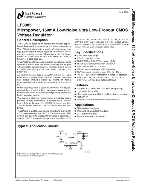
Typical Application Circuit<br />
Note: Pin Numbers in parenthesis indicate micro SMD package.<br />
* Optional Noise Reduction Capacitor.<br />
2.6V, 2.7V, 2.8V, 2.85V, 2.9V, 3.0V. 3.1V, 3.2V, <strong>3.3</strong>V, 4.7V,<br />
4.8V and 5.0V output voltages. For other output voltage<br />
options between 2.5V to 5.0V or for a dual LP3985, please<br />
contact National Semiconductor sales office.<br />
Key Specifications<br />
n 2.5 to 6.0V input range<br />
n 150mA guaranteed output<br />
n 50dB PSRR at 1kHz @ V IN =V OUT + 0.2V<br />
n ≤1.5µA quiescent current when shut down<br />
n Fast Turn-On time: 200 µs (typ.)<br />
n 100mV maximum dropout with 150mA load<br />
n 30µVrms output noise (typ) over 10Hz to 100kHz<br />
n −40 to +125˚C junction temperature range for operation<br />
n 2.5V, 2.6V, 2.7V, 2.8V, 2.85V, 2.9V, 3.0V, 3.1V, 3.2V,<br />
<strong>3.3</strong>V, 4.7V, 4.8V and 5.0V outputs standard<br />
Features<br />
n Miniature 5-I/O micro SMD and SOT-23-5 package<br />
n Logic controlled enable<br />
n Stable with ceramic and high quality tantalum capacitors<br />
n Fast turn-on<br />
n Thermal shutdown and short-circuit current limit<br />
Applications<br />
n CDMA cellular handsets<br />
n Wideband CDMA cellular handsets<br />
n GSM cellular handsets<br />
n Portable information appliances<br />
10136402<br />
June 2003<br />
LP3985 Micropower, 150mA Low-Noise Ultra Low-Dropout CMOS Voltage Regulator<br />
© 2003 National Semiconductor Corporation DS101364 www.national.com
LP3985<br />
Block Diagram<br />
10136401<br />
Pin Description<br />
Name * micro SMD SOT Function<br />
V EN A1 3 Enable Input Logic, Enable High<br />
GND B2 2 Common Ground<br />
V OUT C1 5 Output Voltage of the LDO<br />
V IN C3 1 Input Voltage of the LDO<br />
BYPASS A3 4 Optional Bypass Capacitor for Noise<br />
Reduction<br />
* The pin numbering scheme for the micro SMD package was revised in April 2002 to conform to JEDEC standard. Only the pin numbers were<br />
revised. No changes to the physical location of the inputs/outputs were made. For reference purposes, the obsolete numbering scheme had VEN<br />
as pin 1, GND as pin 2, VOUT as pin 3, VIN as pin 4, and BYPASS as pin 5.<br />
Connection Diagrams<br />
SOT 23-5 Package (MF)<br />
5 Bump micro SMD Package (BPA05, BLA05, TLA05)<br />
10136407<br />
Top View<br />
See NS Package Number MF05A<br />
10136470<br />
Top View<br />
See NS Package Number BPA05, BLA05, TLA05<br />
www.national.com 2
Ordering Information<br />
Output<br />
Voltage (V)<br />
BP refers to 0.170mm bump size, 0.900mm height for micro SMD Package<br />
Grade<br />
LP3985 Supplied as 250<br />
Units, Tape and Reel<br />
LP3985 Supplied as 3000<br />
Units, Tape and Reel<br />
2.5 STD LP3985IBP-2.5 LP3985IBPX-2.5<br />
2.6 STD LP3985IBP-2.6 LP3985IBPX-2.6<br />
2.7 STD LP3985IBP-2.7 LP3985IBPX-2.7<br />
2.8 STD LP3985IBP-2.8 LP3985IBPX-2.8<br />
2.85 STD LP3985IBP-285 LP3985IBPX-285<br />
2.9 STD LP3985IBP-2.9 LP3985IBPX-2.9<br />
3.0 STD LP3985IBP-3.0 LP3985IBPX-3.0<br />
3.1 STD LP3985IBP-3.1 LP3985IBPX-3.1<br />
3.2 STD LP3985IBP-3.2 LP3985IBPX-3.2<br />
<strong>3.3</strong> STD LP3985IBP-<strong>3.3</strong> LP3985IBPX-<strong>3.3</strong><br />
4.7 STD LP3985IBP-4.7 LP3985IBPX-4.7<br />
5.0 STD LP3985IBP-5.0 LP3985IBPX-5.0<br />
LP3985<br />
Output<br />
Voltage (V)<br />
BL refers to 0.300mm bump size, 0.995mm height for micro SMD Package<br />
Grade<br />
LP3985 Supplied as 250<br />
Units, Tape and Reel<br />
LP3985 Supplied as 3000<br />
Units, Tape and Reel<br />
2.5 STD LP3985IBL-2.5 LP3985IBLX-2.5<br />
2.6 STD LP3985IBL-2.6 LP3985IBLX-2.6<br />
2.7 STD LP3985IBL-2.7 LP3985IBLX-2.7<br />
2.8 STD LP3985IBL-2.8 LP3985IBLX-2.8<br />
2.85 STD LP3985IBL-285 LP3985IBLX-285<br />
2.9 STD LP3985IBL-2.9 LP3985IBLX-2.9<br />
3.0 STD LP3985IBL-3.0 LP3985IBLX-3.0<br />
3.1 STD LP3985IBL-3.1 LP3985IBLX-3.1<br />
3.2 STD LP3985IBL-3.2 LP3985IBLX-3.2<br />
<strong>3.3</strong> STD LP3985IBL-<strong>3.3</strong> LP3985IBLX-<strong>3.3</strong><br />
4.8 STD LP3985IBL-4.8 LP3985IBLX-4.8<br />
5.0 STD LP3985IBL-5.0 LP3985IBLX-5.0<br />
Output<br />
Voltage (V)<br />
TL refers to 0.300mm bump size, 0.600mm height for micro SMD Package<br />
Grade<br />
LP3985 Supplied as 250<br />
Units, Tape and Reel<br />
LP3985 Supplied as 3000<br />
Units, Tape and Reel<br />
2.5 STD LP3985ITL-2.5 LP3985ITLX-2.5<br />
2.6 STD LP3985ITL-2.6 LP3985ITLX-2.6<br />
2.7 STD LP3985ITL-2.7 LP3985ITLX-2.7<br />
2.8 STD LP3985ITL-2.8 LP3985ITLX-2.8<br />
2.85 STD LP3985ITL-285 LP3985ITLX-285<br />
2.9 STD LP3985ITL-2.9 LP3985ITLX-2.9<br />
3.0 STD LP3985ITL-3.0 LP3985ITLX-3.0<br />
3.1 STD LP3985ITL-3.1 LP3985ITLX-3.1<br />
3.2 STD LP3985ITL-3.2 LP3985ITLX-3.2<br />
<strong>3.3</strong> STD LP3985ITL-<strong>3.3</strong> LP3985ITLX-<strong>3.3</strong><br />
4.8 STD LP3985ITL-4.8 LP3985ITLX-4.8<br />
5.0 STD LP3985ITL-5.0 LP3985ITLX-5.0<br />
3<br />
www.national.com
LP3985<br />
Ordering Information (Continued)<br />
Output<br />
Voltage (V)<br />
Grade<br />
For SOT Package<br />
LP3985 Supplied as 1000<br />
Units, Tape and Reel<br />
LP3985 Supplied as 3000<br />
Units, Tape and Reel<br />
Package Marking<br />
2.5 STD <strong>LP3985IM5</strong>-2.5 <strong>LP3985IM5</strong>X-2.5 LCSB<br />
2.6 STD <strong>LP3985IM5</strong>-2.6 <strong>LP3985IM5</strong>X-2.6 LCTB<br />
2.7 STD <strong>LP3985IM5</strong>-2.7 <strong>LP3985IM5</strong>X-2.7 LCUB<br />
2.8 STD <strong>LP3985IM5</strong>-2.8 <strong>LP3985IM5</strong>X-2.8 LCJB<br />
2.85 STD <strong>LP3985IM5</strong>-285 <strong>LP3985IM5</strong>X-285 LCXB<br />
2.9 STD <strong>LP3985IM5</strong>-2.9 <strong>LP3985IM5</strong>X-2.9 LCYB<br />
3.0 STD <strong>LP3985IM5</strong>-3.0 <strong>LP3985IM5</strong>X-3.0 LCRB<br />
3.1 STD <strong>LP3985IM5</strong>-3.1 <strong>LP3985IM5</strong>X-3.1 LCZB<br />
3.2 STD <strong>LP3985IM5</strong>-3.2 <strong>LP3985IM5</strong>X-3.2 LDPB<br />
<strong>3.3</strong> STD <strong>LP3985IM5</strong>-<strong>3.3</strong> <strong>LP3985IM5</strong>X-<strong>3.3</strong> LDQB<br />
4.7 STD <strong>LP3985IM5</strong>-4.7 <strong>LP3985IM5</strong>X-4.7 LDRB<br />
5.0 STD <strong>LP3985IM5</strong>-5.0 <strong>LP3985IM5</strong>X-5.0 LDSB<br />
www.national.com 4
Absolute Maximum Ratings (Notes 1,<br />
2)<br />
If Military/Aerospace specified devices are required,<br />
please contact the National Semiconductor Sales Office/<br />
Distributors for availability and specifications.<br />
V IN ,V EN −0.3 to 6.5V<br />
V OUT -0.3 to (V IN +0.3) ≤ 6.5V<br />
Junction Temperature<br />
150˚C<br />
Storage Temperature<br />
−65˚C to +150˚C<br />
Lead Temp.<br />
235˚C<br />
Pad Temp. (Note 3)<br />
235˚C<br />
Maximum Power Dissipation<br />
SOT23-5 (Note 4)<br />
micro SMD (Note 4)<br />
ESD Rating(Note 5)<br />
Human Body Model<br />
Machine Model<br />
Electrical Characteristics<br />
364mW<br />
355mW<br />
2kV<br />
150V<br />
Operating Ratings (Notes 1, 2)<br />
V IN<br />
V EN<br />
Junction Temperature<br />
Thermal Resistance<br />
θ JA (SOT23-5)<br />
θ JA (micro SMD)<br />
Maximum Power Dissipation<br />
SOT23-5 (Note 6)<br />
micro SMD (Note 6)<br />
2.5 to 6V<br />
0to(V IN +0.3) ≤ 6V<br />
−40˚C to +125˚C<br />
220˚C/W<br />
255˚C/W<br />
250mW<br />
244mW<br />
LP3985<br />
Unless otherwise specified: V IN =V OUT(nom) + 0.5V, C IN = 1 µF, I OUT = 1mA, C OUT = 1 µF, C BYPASS = 0.01µF. Typical values<br />
and limits appearing in standard typeface are for T J = 25˚C. Limits appearing in boldface type apply over the entire junction<br />
temperature range for operation, −40˚C to +125˚C. (Note 7) (Note 8)<br />
Symbol Parameter Conditions Typ<br />
∆V OUT<br />
PSRR<br />
Output Voltage<br />
Tolerance<br />
Line Regulation Error<br />
Load Regulation Error<br />
(Note 9)<br />
I OUT = 1mA<br />
V IN =(V OUT(nom) + 0.5V) to 6.0V,<br />
For 4.7 to 5.0 options<br />
For all other options<br />
Output AC Line Regulation V IN =V OUT(nom) + 1V,<br />
I OUT = 150 mA (Figure 1)<br />
Power Supply Rejection Ratio<br />
Min<br />
−2<br />
−3<br />
−0.19<br />
−0.1<br />
Limit<br />
Max<br />
2<br />
3<br />
0.19<br />
0.1<br />
I OUT = 1 mA to 150 mA<br />
0.0025 0.005<br />
<strong>LP3985IM5</strong> (SOT23-5)<br />
LP3985 (micro SMD) 0.0004 0.002<br />
V IN =V OUT(nom) + 0.2V,<br />
f = 1 kHz,<br />
I OUT =50mA(Figure 2)<br />
V IN =V OUT(nom) + 0.2V,<br />
f = 10 kHz,<br />
I OUT =50mA(Figure 2)<br />
I Q Quiescent Current V EN = 1.4V, I OUT =0mA<br />
For 4.7 to 5.0 options<br />
For all other options<br />
V EN = 1.4V, I OUT = 0 to 150 mA<br />
For 4.7 to 5.0 options<br />
For all other options<br />
V EN = 0.4V 0.003 1.5<br />
Dropout Voltage (Note 10) I OUT =1mA 0.4 2<br />
1.5<br />
50<br />
40<br />
100<br />
85<br />
155<br />
140<br />
165<br />
150<br />
250<br />
200<br />
Units<br />
%of<br />
V OUT(nom)<br />
I OUT =50mA 20 35<br />
mV<br />
I OUT = 100 mA 45 70<br />
I OUT = 150 mA 60 100<br />
I SC Short Circuit Current Limit Output Grounded<br />
600<br />
mA<br />
(Steady State)<br />
I OUT(PK) Peak Output Current V OUT ≥ V OUT(nom) - 5% 550 300 mA<br />
%/V<br />
%/mA<br />
mV P-P<br />
dB<br />
µA<br />
5<br />
www.national.com
LP3985<br />
Electrical Characteristics (Continued)<br />
Unless otherwise specified: V IN =V OUT(nom) + 0.5V, C IN = 1 µF, I OUT = 1mA, C OUT = 1 µF, C BYPASS = 0.01µF. Typical values<br />
and limits appearing in standard typeface are for T J = 25˚C. Limits appearing in boldface type apply over the entire junction<br />
temperature range for operation, −40˚C to +125˚C. (Note 7) (Note 8)<br />
Symbol Parameter Conditions Typ<br />
Limit<br />
Min Max<br />
Units<br />
T ON Turn-On Time<br />
C BYPASS = 0.01 µF 200<br />
(Note 11)<br />
µs<br />
e n Output Noise Voltage(Note 12) BW = 10 Hz to 100 kHz,<br />
30 µVrms<br />
C OUT = 1µF<br />
Output Noise Density C BP = 0 230 nV/<br />
I EN Maximum Input Current at EN V EN = 0.4 and V IN = 6.0 ±1 nA<br />
V IL Maximum Low Level Input V IN = 2.5 to 6.0V 0.4 V<br />
Voltage at EN<br />
V IH Minimum High Level Input V IN = 2.5 to 6.0V 1.4 V<br />
Voltage at EN<br />
C OUT Output Capacitor Capacitance 1 20 µF<br />
ESR 5 500 mΩ<br />
TSD<br />
Thermal Shutdown Temperature 160 ˚C<br />
Thermal Shutdown Hysteresis 20 ˚C<br />
Note 1: Absolute Maximum Ratings are limits beyond which damage to the device may occur. Operating Ratings are conditions under which operation of the device<br />
is guaranteed. Operating Ratings do not imply guaranteed performance limits. For guaranteed performance limits and associated test conditions, see the Electrical<br />
Characteristics tables.<br />
Note 2: All voltages are with respect to the potential at the GND pin.<br />
Note 3: Additional information on lead temperature and pad temperature can be found in National Semiconductor Application Note (AN-1112).<br />
Note 4: The Absolute Maximum power dissipation depends on the ambient temperature and can be calculated using the formula: P D =(T J -T A )/θ JA ,<br />
where T J is the junction temperature, T A is the ambient temperature, and θ JA is the junction-to-ambient thermal resistance. The 364mW rating for SOT23-5<br />
appearing under Absolute Maximum Ratings results from substituting the Absolute Maximum junction temperature, 150˚C, for T J , 70˚C for T A , and 220˚C/W for θ JA .<br />
More power can be dissipated safely at ambient temperatures below 70˚C . Less power can be dissipated safely at ambient temperatures above 70˚C. The Absolute<br />
Maximum power dissipation can be increased by 4.5mW for each degree below 70˚C, and it must be derated by 4.5mW for each degree above 70˚C.<br />
Note 5: The human body model is 100pF discharged through 1.5kΩ resistor into each pin. The machine model is a 200 pF capacitor discharged directly into each<br />
pin.<br />
Note 6: Like the Absolute Maximum power dissipation, the maximum power dissipation for operation depends on the ambient temperature. The 250mW rating for<br />
SOT23-5 appearing under Operating Ratings results from substituting the maximum junction temperature for operation, 125˚C, for T J , 70˚C for T A , and 220˚C/W for<br />
θ JA into (Note 4) above. More power can be dissipated at ambient temperatures below 70˚C . Less power can be dissipated at ambient temperatures above 70˚C.<br />
The maximum power dissipation for operation can be increased by 4.5mW for each degree below 70˚C, and it must be derated by 4.5mW for each degree above<br />
70˚C.<br />
Note 7: All limits are guaranteed. All electrical characteristics having room-temperature limits are tested during production with T J = 25˚C or correlated using<br />
Statistical Quality Control (SQC) methods. All hot and cold limits are guaranteed by correlating the electrical characteristics to process and temperature variations<br />
and applying statistical process control.<br />
Note 8: The target output voltage, which is labeled V OUT(nom) , is the desired voltage option.<br />
Note 9: An increase in the load current results in a slight decrease in the output voltage and vice versa.<br />
Note 10: Dropout voltage is the input-to-output voltage difference at which the output voltage is 100mV below its nominal value. This specification does not apply<br />
for input voltages below 2.5V.<br />
Note 11: Turn-on time is time measured between the enable input just exceeding V IH and the output voltage just reaching 95% of its nominal value.<br />
Note 12: The output noise varies with output voltage option. The 30µVrms is measured with 2.5V voltage option. To calculate an approximated output noise for other<br />
options, use the equation: (30µVrms)(X)/2.5, where X is the voltage option value.<br />
10136408<br />
FIGURE 1. Line Transient Input Test Signal<br />
www.national.com 6
LP3985<br />
10136409<br />
FIGURE 2. PSRR Input Test Signal<br />
Typical Performance Characteristics Unless otherwise specified, C IN =C OUT = 1 µF Ceramic,<br />
C BYPASS = 0.01 µF, V IN =V OUT + 0.2V, T A = 25˚C, Enable pin is tied to V IN .<br />
Output Voltage Change vs Temperature<br />
Dropout Voltage vs Load Current<br />
10136441<br />
10136433<br />
Ground Current vs Load Current<br />
Ground Current vs V IN @ 25˚C<br />
10136440<br />
10136435<br />
7<br />
www.national.com
LP3985<br />
Typical Performance Characteristics Unless otherwise specified, C IN =C OUT = 1 µF Ceramic,<br />
C BYPASS = 0.01 µF, V IN =V OUT + 0.2V, T A = 25˚C, Enable pin is tied to V IN . (Continued)<br />
Ground Current vs V IN @ −40˚C<br />
Ground Current vs V IN @ 125˚C<br />
10136437 10136439<br />
Short Circuit Current (micro SMD)<br />
Short Circuit Current (micro SMD)<br />
10136445 10136446<br />
Short Circuit Current (SOT)<br />
Short Circuit Current (SOT)<br />
10136447 10136448<br />
www.national.com 8
Typical Performance Characteristics Unless otherwise specified, C IN =C OUT = 1 µF Ceramic,<br />
C BYPASS = 0.01 µF, V IN =V OUT + 0.2V, T A = 25˚C, Enable pin is tied to V IN . (Continued)<br />
LP3985<br />
Short Circuit Current (SOT)<br />
Short Circuit Current (SOT)<br />
10136449 10136450<br />
Short Circuit Current (micro SMD)<br />
Short Circuit Current (micro SMD)<br />
10136451 10136452<br />
Output Noise Spectral Density<br />
Ripple Rejection (V IN =V OUT + 0.2V)<br />
10136410 10136411<br />
9<br />
www.national.com
LP3985<br />
Typical Performance Characteristics Unless otherwise specified, C IN =C OUT = 1 µF Ceramic,<br />
C BYPASS = 0.01 µF, V IN =V OUT + 0.2V, T A = 25˚C, Enable pin is tied to V IN . (Continued)<br />
Ripple Rejection (V IN =V OUT + 1V)<br />
Ripple Rejection (V IN = 5.0V)<br />
10136412 10136413<br />
Start Up Time (V IN =V OUT + 0.2V)<br />
Start Up Time (V IN = 4.2V)<br />
10136414 10136415<br />
Start Up Time (V IN =V OUT + 0.2V)<br />
Start Up Time (V IN = 4.2V)<br />
10136416 10136417<br />
www.national.com 10
Typical Performance Characteristics Unless otherwise specified, C IN =C OUT = 1 µF Ceramic,<br />
C BYPASS = 0.01 µF, V IN =V OUT + 0.2V, T A = 25˚C, Enable pin is tied to V IN . (Continued)<br />
LP3985<br />
Start Up Time (V IN =V OUT + 0.2V)<br />
Start Up Time (V IN = 4.2V)<br />
10136418 10136419<br />
Line Transient Response<br />
Line Transient Response<br />
10136420 10136421<br />
Load Transient Response (V IN = 3.2V)<br />
Load Transient Response (V IN = 4.2V)<br />
10136423 10136422<br />
11<br />
www.national.com
LP3985<br />
Typical Performance Characteristics Unless otherwise specified, C IN =C OUT = 1 µF Ceramic,<br />
C BYPASS = 0.01 µF, V IN =V OUT + 0.2V, T A = 25˚C, Enable pin is tied to V IN . (Continued)<br />
Load Transient Response (V IN = 3.2V)<br />
Load Transient Response (V IN = 4.2V)<br />
10136424 10136425<br />
Enable Response (V IN =V OUT + 0.2V)<br />
Enable Response (V IN = 4.2V)<br />
10136453 10136454<br />
Enable Response (V IN =V OUT + 0.2V)<br />
Enable Response (V IN = 4.2V)<br />
10136455 10136456<br />
www.national.com 12
Typical Performance Characteristics Unless otherwise specified, C IN =C OUT = 1 µF Ceramic,<br />
C BYPASS = 0.01 µF, V IN =V OUT + 0.2V, T A = 25˚C, Enable pin is tied to V IN . (Continued)<br />
LP3985<br />
Output Impedance (V IN = 4.2V)<br />
Output Impedance (V IN =V OUT + 0.2V)<br />
10136465 10136466<br />
Application Hints<br />
EXTERNAL CAPACITORS<br />
Like any low-dropout regulator, the LP3985 requires external<br />
capacitors for regulator stability. The LP3985 is specifically<br />
designed for portable applications requiring minimum board<br />
space and smallest components. These capacitors must be<br />
correctly selected for good performance.<br />
INPUT CAPACITOR<br />
An input capacitance of ) 1µF is required between the<br />
LP3985 input pin and ground (the amount of the capacitance<br />
may be increased without limit).<br />
This capacitor must be located a distance of not more than<br />
1cm from the input pin and returned to a clean analog<br />
ground. Any good quality ceramic, tantalum, or film capacitor<br />
may be used at the input.<br />
Important: Tantalum capacitors can suffer catastrophic failures<br />
due to surge current when connected to a lowimpedance<br />
source of power (like a battery or a very large<br />
capacitor). If a tantalum capacitor is used at the input, it must<br />
be guaranteed by the manufacturer to have a surge current<br />
rating sufficient for the application.<br />
There are no requirements for the ESR on the input capacitor,<br />
but tolerance and temperature coefficient must be considered<br />
when selecting the capacitor to ensure the capacitance<br />
will be ) 1µF over the entire operating temperature<br />
range.<br />
OUTPUT CAPACITOR<br />
The LP3985 is designed specifically to work with very small<br />
ceramic output capacitors. A ceramic capacitor (temperature<br />
characteristics X7R, X5R, Z5U, or Y5V) in 1 to 22 µF range<br />
with 5mΩ to 500mΩ ESR range is suitable in the LP3985<br />
application circuit.<br />
It may also be possible to use tantalum or film capacitors at<br />
the output, but these are not as attractive for reasons of size<br />
and cost (see next section Capacitor Characteristics).<br />
The output capacitor must meet the requirement for minimum<br />
amount of capacitance and also have an ESR (Equivalent<br />
Series Resistance) value which is within a stable range<br />
(5 mΩ to 500 mΩ).<br />
NO-LOAD STABILITY<br />
The LP3985 will remain stable and in regulation with no<br />
external load. This is specially important in CMOS RAM<br />
keep-alive applications.<br />
CAPACITOR CHARACTERISTICS<br />
The LP3985 is designed to work with ceramic capacitors on<br />
the output to take advantage of the benefits they offer: for<br />
capacitance values in the range of 1µF to 4.7µF range,<br />
ceramic capacitors are the smallest, least expensive and<br />
have the lowest ESR values (which makes them best for<br />
eliminating high frequency noise). The ESR of a typical 1µF<br />
ceramic capacitor is in the range of 20 mΩ to 40 mΩ, which<br />
easily meets the ESR requirement for stability by the<br />
LP3985.<br />
The ceramic capacitor’s capacitance can vary with temperature.<br />
The capacitor type X7R, which operates over a temperature<br />
range of -55˚C to +125˚C, will only vary the capacitance<br />
to within ±15%. Most large value ceramic capacitors<br />
() 2.2µF) are manufactured with Z5U or Y5V temperature<br />
characteristics. Their capacitance can drop by more than<br />
50% as the temperature goes from 25˚C to 85˚C. Therefore,<br />
X7R is recommended over Z5U and Y5V in applications<br />
where the ambient temperature will change significantly<br />
above or below 25˚C.<br />
Tantalum capacitors are less desirable than ceramic for use<br />
as output capacitors because they are more expensive when<br />
comparing equivalent capacitance and voltage ratings in the<br />
1µF to 4.7µF range.<br />
Another important consideration is that tantalum capacitors<br />
have higher ESR values than equivalent size ceramics. This<br />
means that while it may be possible to find a tantalum<br />
capacitor with an ESR value within the stable range, it would<br />
have to be larger in capacitance (which means bigger and<br />
more costly ) than a ceramic capacitor with the same ESR<br />
value. It should also be noted that the ESR of a typical<br />
tantalum will increase about 2:1 as the temperature goes<br />
from 25˚C down to −40˚C, so some guard band must be<br />
allowed.<br />
NOISE BYPASS CAPACITOR<br />
Connecting a 0.01µF capacitor between the C BYPASS pin<br />
and ground significantly reduces noise on the regulator output.<br />
This cap is connected directly to a high impedance node<br />
13<br />
www.national.com
LP3985<br />
Application Hints (Continued)<br />
in the band gap reference circuit. Any significant loading on<br />
this node will cause a change on the regulated output voltage.<br />
For this reason, DC leakage current through this pin<br />
must be kept as low as possible for best output voltage<br />
accuracy.<br />
The types of capacitors best suited for the noise bypass<br />
capacitor are ceramic and film. High-quality ceramic capacitors<br />
with either NPO or COG dielectric typically have very<br />
low leakage. Polypropolene and polycarbonate film capacitors<br />
are available in small surface-mount packages and<br />
typically have extremely low leakage current.<br />
Unlike many other LDO’s, addition of a noise reduction<br />
capacitor does not effect the load transient response of the<br />
device.<br />
ON/OFF INPUT OPERATION<br />
The LP3985 is turned off by pulling the V EN pin low, and<br />
turned on by pulling it high. If this feature is not used, the V EN<br />
pin should be tied to V IN to keep the regulator output on at all<br />
time. To assure proper operation, the signal source used to<br />
drive the V EN input must be able to swing above and below<br />
the specified turn-on/off voltage thresholds listed in the Electrical<br />
Characteristics section under V IL and V IH .<br />
FAST ON-TIME<br />
The LP3985 output is turned on after Vref voltage reaches its<br />
final value (1.23V nomial). To speed up this process, the<br />
noise reduction capacitor at the bypass pin is charged with<br />
an internal 70uA current source. The current source is turned<br />
off when the bandgap voltage reaches approximately 95% of<br />
its final value. The turn on time is determined by the time<br />
constant of the bypass capacitor. The smaller the capacitor<br />
value, the shorter the turn on time, but less noise gets<br />
reduced. As a result, turn on time and noise reduction need<br />
to be taken into design consideration when choosing the<br />
value of the bypass capacitor.<br />
micro SMD MOUNTING<br />
The micro SMD package requires specific mounting techniques<br />
which are detailed in National Semiconductor Application<br />
Note (AN-1112). Referring to the section Surface<br />
Mount Technology (SMT) Assembly Considerations, it<br />
should be noted that the pad style which must be used with<br />
the 5 pin package is NSMD (non-solder mask defined) type.<br />
For best results during assembly, alignment ordinals on the<br />
PC board may be used to facilitate placement of the micro<br />
SMD device.<br />
micro SMD LIGHT SENSITIVITY<br />
Exposing the micro SMD device to direct sunlight will cause<br />
misoperation of the device. Light sources such as halogen<br />
lamps can effect electrical performance if brought near to the<br />
device.<br />
The wavelengths which have most detrimental effect are<br />
reds and infra-reds, which means that the fluorescent lighting<br />
used inside most buildings has very little effect on performance.<br />
A micro SMD test board was brought to within<br />
1cm of a fluorescent desk lamp and the effect on the regulated<br />
output voltage was negligible, showing a deviation of<br />
less than 0.1% from nominal.<br />
www.national.com 14
Physical Dimensions inches (millimeters)<br />
unless otherwise noted<br />
LP3985<br />
5-Lead Small Outline Package (MF)<br />
NS Package Number MF05A<br />
micro SMD, 5 Bump, Package (BPA05)<br />
NS Package Number BPA05CMC<br />
The dimensions for X1, X2 and X3 are as given:<br />
X1 = 0.828 +/− 0.03mm<br />
X2 = 1.387 +/− 0.03mm<br />
X3 = 0.900 +/− 0.10mm<br />
15<br />
www.national.com
LP3985<br />
Physical Dimensions inches (millimeters) unless otherwise noted (Continued)<br />
micro SMD, 5 Bump, Package (BLA05)<br />
NS Package Number BLA05ADC<br />
The dimensions for X1, X2 and X3 are as given:<br />
X1 = 1.006 +/- 0.03mm<br />
X2 = 1.438 +/- 0.03mm<br />
X3 = 0.995 +/- 0.10mm<br />
www.national.com 16
Physical Dimensions inches (millimeters) unless otherwise noted (Continued)<br />
LIFE SUPPORT POLICY<br />
thin micro SMD, 5 Bump, Package (TLA05)<br />
NS Package Number TLA05ADA<br />
The dimensions for X1, X2 and X3 are as given:<br />
X1 = 1.006 +/- 0.03mm<br />
X2 = 1.438 +/- 0.03mm<br />
X3 = 0.6 +/- 0.075mm<br />
NATIONAL’S PRODUCTS ARE NOT AUTHORIZED FOR USE AS CRITICAL COMPONENTS IN LIFE SUPPORT<br />
DEVICES OR SYSTEMS WITHOUT THE EXPRESS WRITTEN APPROVAL OF THE PRESIDENT AND GENERAL<br />
COUNSEL OF NATIONAL SEMICONDUCTOR CORPORATION. As used herein:<br />
1. Life support devices or systems are devices or<br />
systems which, (a) are intended for surgical implant<br />
into the body, or (b) support or sustain life, and<br />
whose failure to perform when properly used in<br />
accordance with instructions for use provided in the<br />
labeling, can be reasonably expected to result in a<br />
significant injury to the user.<br />
2. A critical component is any component of a life<br />
support device or system whose failure to perform<br />
can be reasonably expected to cause the failure of<br />
the life support device or system, or to affect its<br />
safety or effectiveness.<br />
LP3985 Micropower, 150mA Low-Noise Ultra Low-Dropout CMOS Voltage Regulator<br />
National Semiconductor<br />
Americas Customer<br />
Support Center<br />
Email: new.feedback@nsc.com<br />
Tel: 1-800-272-9959<br />
www.national.com<br />
National Semiconductor<br />
Europe Customer Support Center<br />
Fax: +49 (0) 180-530 85 86<br />
Email: europe.support@nsc.com<br />
Deutsch Tel: +49 (0) 69 9508 6208<br />
English Tel: +44 (0) 870 24 0 2171<br />
Français Tel: +33 (0) 1 41 91 8790<br />
National Semiconductor<br />
Asia Pacific Customer<br />
Support Center<br />
Email: ap.support@nsc.com<br />
National Semiconductor<br />
Japan Customer Support Center<br />
Fax: 81-3-5639-7507<br />
Email: jpn.feedback@nsc.com<br />
Tel: 81-3-5639-7560<br />
National does not assume any responsibility for use of any circuitry described, no circuit patent licenses are implied and National reserves the right at any time without notice to change said circuitry and specifications.