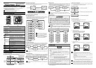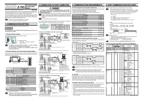
Z-TIO Host Communication Quick Instruction ... - rkc instrument inc.
Z-TIO Host Communication Quick Instruction ... - rkc instrument inc.
Z-TIO Host Communication Quick Instruction ... - rkc instrument inc.

You also want an ePaper? Increase the reach of your titles
YUMPU automatically turns print PDFs into web optimized ePapers that Google loves.
Module Type Controller SRZ<br />
Temperature Control Module<br />
[for <strong>Host</strong> <strong>Communication</strong>]<br />
All Rights Reserved, Copyright © 2006, RKC INSTRUMENT INC.<br />
IMS01T02-E3<br />
Thank you for purchasing this RKC product. In order to achieve maximum performance and<br />
ensure proper operation of your new <strong>instrument</strong>, carefully read all the instructions in this<br />
manual. Please place this manual in a convenient location for easy reference.<br />
This manual describes the host communication, module address setting of the Z-<strong>TIO</strong><br />
module. For the address setting of any other module, refer to the <strong>Instruction</strong> Manual for the<br />
respective module. For detailed handling procedures and various function settings, please<br />
refer to separate SRZ <strong>Instruction</strong> Manual (IMS01T04 -E).<br />
The above manuals can be downloaded from our website:<br />
URL: http://www.<strong>rkc</strong>inst.com/english/manual_load.htm<br />
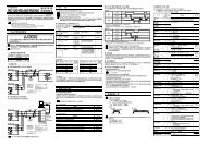
1. COMMUNICA<strong>TIO</strong>N SETTING<br />
Set communication setting before mounting and wiring of the Z-<strong>TIO</strong>.<br />
CAU<strong>TIO</strong>N<br />
Do not separate the module mainframe from the base with the power turned on. If so,<br />
<strong>instrument</strong> failure may result.<br />
1.1 Module Address Setting<br />
Set an address for the module using a small blade screwdriver.<br />
Address setting switch<br />
Setting range: 0 to F [0 to 15: Decimal]<br />
Factory set value: 0<br />
• For Modbus, the value obtained by adding “1” to the set address<br />
corresponds to the address used for the actual program.<br />
• To avoid problems or malfunction, do not duplicate an address on the<br />
same communication line.<br />
1.2 Protocol Selections and <strong>Communication</strong> Speed Setting<br />
Use the DIP switch on the right side of module to select communication speed, data bit<br />
configuration and protocol. The data changes become valid when the power is turned on<br />
again or when changed to RUN/STOP.<br />
Right side view<br />
Module<br />
mainframe<br />
DIP switch<br />
(The above figure is for the terminal type. However, the switch positions are the same for the connector type.)<br />
1 2 <strong>Communication</strong> speed<br />
OFF OFF 4800 bps<br />
ON OFF 9600 bps<br />
OFF ON 19200 bps<br />
ON ON 38400 bps<br />
Factory set value: 19200 bps<br />
1 2 3 4 5 6 7 8<br />
OFF<br />
3 4 5 Data bit configuration<br />
OFF OFF OFF Data 7-bit, without parity, Stop 1-bit *<br />
ON OFF OFF Don't set this one<br />
OFF ON OFF Data 7-bit, Even parity, Stop 1-bit *<br />
ON ON OFF Data 7-bit, Odd parity, Stop 1-bit *<br />
OFF OFF ON Data 8-bit, without parity, Stop 1-bit<br />
ON OFF ON Don't set this one<br />
OFF ON ON Data 8-bit, Even parity, Stop 1-bit<br />
ON ON ON Data 8-bit, Odd parity, Stop 1-bit<br />
* When the Modbus communication protocol is selected, this setting becomes invalid.<br />
Factory set value: Data 8-bit, without parity, Stop 1-bit<br />
6 Protocol<br />
OFF<br />
ON<br />
Factory set value: RKC communication<br />
Z-<strong>TIO</strong><br />
RKC communication<br />
Modbus<br />
<strong>Host</strong> <strong>Communication</strong><br />
<strong>Quick</strong> <strong>Instruction</strong><br />
Manual<br />
• Switch No. 7 and 8 must be always OFF. Do not set to ON.<br />
• When two or more modules are connected on the same communication<br />
line, the DIP switch settings of all modules must be the same.<br />
ON<br />
ON<br />
2. CONNEC<strong>TIO</strong>N TO HOST COMPUTER<br />
! WARNING<br />
To prevent electric shock or <strong>instrument</strong> failure, turn off the<br />
power before connecting or disconnecting the <strong>instrument</strong> and<br />
peripheral equipment.<br />
Connect a termination resistor between the communication terminals (No.3<br />
and No. 4) of the module at the end of the communication line from the host<br />
computer.<br />
The cable must be provided by the customer.<br />
The Z-<strong>TIO</strong> has RS-485 communication terminals for RKC communication or Modbus/RTU<br />
communication protocol. <strong>Communication</strong> terminals are on the base side.<br />
• Connection to the RS-485 port of the host computer (master)<br />
Module type controller SRZ<br />
Z-<strong>TIO</strong> module<br />
(Slave)<br />
(−)<br />
(+)<br />
(−)<br />
(+)<br />
•<br />
•<br />
•<br />
T/R (A) 3<br />
T/R (B)<br />
4<br />
SG 5<br />
Z-<strong>TIO</strong> module<br />
(Slave)<br />
T/R (A) 3<br />
T/R (B)<br />
4<br />
SG 5<br />
RS-485<br />
Pair wire<br />
Shielded twisted<br />
Connected by pair wire<br />
the internal<br />
communication line<br />
R<br />
R<br />
<strong>Host</strong> computer (Master)<br />
T/R (A)<br />
T/R (B)<br />
Up to 16 Z-<strong>TIO</strong> modules can be connected.<br />
The maximum number of SRZ modules (<strong>inc</strong>luding other function modules) on the same communication line is 31.<br />
SG<br />
R: Termination resistor (Example: 120 Ω 1/2 W)<br />
• Connection to the RS-232C port of the host computer (master)<br />
Module type controller SRZ<br />
(−)<br />
(+)<br />
(−)<br />
(+)<br />
•<br />
•<br />
•<br />
Z-<strong>TIO</strong> module<br />
(Slave)<br />
T/R (A) 3<br />
T/R (B)<br />
4<br />
SG 5<br />
Z-<strong>TIO</strong> module<br />
(Slave)<br />
T/R (A) 3<br />
T/R (B)<br />
4<br />
SG 5<br />
RS-485<br />
Shielded twisted<br />
pair wire<br />
Connected by<br />
the internal<br />
communication line<br />
R<br />
Pair wire<br />
(−)<br />
(+)<br />
<strong>Host</strong> computer (Master)<br />
R<br />
T/R (A)<br />
T/R (B)<br />
SG<br />
RS-232C<br />
RS-232C/RS-485 converter *<br />
* When the host computer (master) uses<br />
Windows95/98/Me/NT/2000/XP, use a<br />
RS-232C/RS-485 converter with an<br />
automatic send/receive transfer function.<br />
Recommended RS-232C/RS-485 converter:<br />
R: Termination resistor<br />
CD485, CD485/Vmanufactured by Data Link,<br />
(Example: 120 Ω 1/2 W)<br />
Inc. or equivalent<br />
Up to 16 Z-<strong>TIO</strong> modules can be connected.<br />
The maximum number of SRZ modules (<strong>inc</strong>luding other function modules) on the same communication line is 31.<br />
• Connection to the USB of the host computer (master)<br />
Module type controller SRZ<br />
(−)<br />
(+)<br />
(−)<br />
(+)<br />
•<br />
•<br />
•<br />
(Base)<br />
3 4 5<br />
Z-<strong>TIO</strong> module<br />
(Slave)<br />
T/R (A) 3<br />
T/R (B)<br />
4<br />
SG 5<br />
Z-<strong>TIO</strong> module<br />
(Slave)<br />
T/R (A) 3<br />
T/R (B)<br />
4<br />
SG 5<br />
<strong>Communication</strong> terminals (RS-485)<br />
Terminal No. Signal name<br />
3 Send data/Receive data<br />
4 Send data/Receive data<br />
5<br />
Signal ground<br />
RS-485<br />
Pair wire<br />
Shielded twisted<br />
pair wire<br />
Connected by<br />
the internal<br />
communication line<br />
R<br />
<strong>Host</strong> computer (Master)<br />
1 SG<br />
2 T/R (A)<br />
3 T/R(B)<br />
4<br />
Unused<br />
5<br />
USB communication<br />
converter COM-K *<br />
Symbol<br />
T/R (A)<br />
T/R (B)<br />
SG<br />
Connected to USB port<br />
of a personal computer<br />
USB cable<br />
(COM-K<br />
accessory)<br />
Connected to<br />
USB connector<br />
* The termination resistor is built-in to<br />
the COM-K.<br />
R: Termination resistor<br />
(Example: 120 Ω 1/2 W)<br />
Up to 16 Z-<strong>TIO</strong> modules can be connected.<br />
The maximum number of SRZ modules (<strong>inc</strong>luding other function modules) on the same communication line is 31.<br />
3. COMMUNICA<strong>TIO</strong>N REQUIREMENTS<br />
• Processing times during data send/receive<br />
When the host computer is using either the polling or selecting procedure for communication,<br />
the following processing times are required for controller to send data:<br />
- Response wait time after controller sends BCC in polling procedure<br />
- Response wait time after controller sends ACK or NAK in selecting procedure<br />
RKC communication (Polling procedure)<br />
Procedure details<br />
Response send time after controller receives ENQ<br />
Response send time after controller receives ACK<br />
Response send time after controller receives NAK<br />
Response send time after controller sends BCC<br />
RKC communication (Selecting procedure)<br />
Procedure details<br />
Response send time after controller receives BCC<br />
Response wait time after controller sends ACK<br />
Response wait time after controller sends NAK<br />
Modbus<br />
Procedure details<br />
Read holding registers [03H]<br />
Response send time after the slave receives the query message<br />
Preset single register [06H]<br />
Response send time after the slave receives the query message<br />
Diagnostics (loopback test) [08H]<br />
Response send time after the slave receives the query message<br />
Preset multiple registers [10H]<br />
Response send time after the slave receives the query message<br />
• RS-485 (2-wire system) send/receive timing<br />
Time<br />
50 ms max.<br />
50 ms max.<br />
50 ms max.<br />
2 ms max.<br />
Time<br />
50 ms max.<br />
2 ms max.<br />
2 ms max.<br />
Time<br />
50 ms max.<br />
30 ms max.<br />
30 ms max.<br />
100 ms max.<br />
RS-485 communication is conducted through two wires, therefore the transmission and<br />
reception of data requires precise timing.<br />
Polling procedure<br />
<strong>Host</strong><br />
computer<br />
SRZ<br />
Send data Possible<br />
(Possible/Impossible) Impossible<br />
Sending status<br />
Send data Possible<br />
(Possible/Impossible) Impossible<br />
Sending status<br />
a: Response send time after the controller receives [ENQ] + Interval time<br />
b: Response send time after the controller sends BCC<br />
c: Response send time after the controller receives [ACK] + Interval time or<br />
Response send time after the controller receives [NAK] + Interval time<br />
Selecting procedure<br />
<strong>Host</strong><br />
computer<br />
Send data Possible<br />
(Possible/Impossible) Impossible<br />
Sending status<br />
E<br />
O<br />
T<br />
E<br />
A<br />
- - - - - N<br />
C or<br />
Q<br />
K<br />
a<br />
S<br />
TX<br />
S<br />
TX<br />
B<br />
CC<br />
or<br />
- - - - -<br />
- - - - -<br />
Send data Possible<br />
a b<br />
(Possible/Impossible) Impossible<br />
SRZ<br />
Sending status<br />
A N<br />
C AK<br />
K<br />
a: Response send time after the controller receives BCC + Interval time<br />
b: Response wait time after the controller sends ACK or Response wait time after the controller sends NAK<br />
To switch the host computer from transmission to reception, send data must be on<br />
line.<br />
The following processing times are requires for the controller to process data.<br />
- In Polling procedure, Response wait time after the controller sends BCC<br />
- In Selecting procedure, Response wait time after the controller sends ACK or NAK<br />
• Fail-safe<br />
A transmission error may occur with the transmission line disconnected, shorted or set to the<br />
high-impedance state. In order to prevent the above error, it is recommended that the<br />
fail-safe function be provided on the receiver side of the host computer. The fail-safe function<br />
can prevent a framing error from its occurrence by making the receiver output stable to the<br />
MARK (1) when the transmission line is in the high-impedance state.<br />
• Modbus data processing precautions<br />
• Data with decimal point is treated as data without decimal point on the Modbus protocol.<br />
• With Modbus protocol, the maximum number of channels per slave address is 4.<br />
• Do not write data to any address which is not described in a list of data maps.<br />
• If data range or address error occurs during data writing, the data written before error is in<br />
effect.<br />
• When communication data is sent to the controller that does not correctly match the<br />
connected module or selected functions on the modules, the data will be invalid. If the<br />
data is within a setting range, no error message is sent from the controller. The read data<br />
is “0”.<br />
• Send the next command message at time intervals of 24 bits after the master receives the<br />
response message.<br />
B<br />
CC<br />
b<br />
c<br />
N<br />
A<br />
K<br />
4. HOST COMMUNICA<strong>TIO</strong>N DATA MAP<br />
Explanation of items shown in the communication data maps are as follows.<br />
• Modbus register address (HEX: Hexadecimal DEC: Decimal)<br />
For a 4CH type, follow the chart exactly. For the 2CH type, the register<br />
addresses for Channel 3 and 4 are unused. For communication parameters for<br />
heat/cool control, the register addresses for Channel 2 and 4 are unused.<br />
Example: The register addresses of 0092 (HEX) to 0095 (HEX)<br />
CH# Address<br />
・<br />
・<br />
CH1 0092<br />
CH2 0093 (This address is unused with heat/cool control.)<br />
CH3 0094 (This address is unused with 2CH type.)<br />
CH4 0095 (This address is unused with heat/cool control or 2CH type.)<br />
・<br />
・<br />
• Digits<br />
The number of communication data digits in RKC communication<br />
• Attribute<br />
RO: Read only data (<strong>Host</strong> computer The controller)<br />
R/W: Read and Write data (<strong>Host</strong> computer The controller)<br />
• Data<br />
RKC communication<br />
Modbus<br />
ASCII code data (Example: 7 digits) 16-bit data<br />
Most significant<br />
digit<br />
…… Least significant b15 …………….…………………… b0<br />
digit<br />
Symbols used in MAP<br />
♣: Parameters only used for heat/cool control or position proportioning control,<br />
therefore data for CH2 and CH4 are unused.<br />
: Parameters which can be used in multi-memory area function.<br />
♦: Data for each module ♠: Data for each channel<br />
For details on the data, see the SRZ <strong>Instruction</strong> Manual (IMS01T04-E).<br />
• <strong>Communication</strong> data (RKC communication/Modbus)<br />
RKC Modbus<br />
Name Iden- register address Digits Attribute<br />
Factory<br />
Data range<br />
set value<br />
tifier HEX DEC<br />
Model code ♦ ID ⎯ ⎯ 32 RO Model code (character) ⎯<br />
ROM version ♦ VR ⎯ ⎯ 8 RO ROM version ⎯<br />
Measured value<br />
(PV)<br />
♠<br />
Comprehensive<br />
event state<br />
♠<br />
Operation mode<br />
state monitor<br />
♠<br />
Error code<br />
♦<br />
M1 0000<br />
・<br />
0003<br />
AJ 0004<br />
・<br />
0007<br />
L0 0008<br />
・<br />
000B<br />
0<br />
・<br />
3<br />
4<br />
・<br />
7<br />
8<br />
・<br />
11<br />
7 RO Input scale low to<br />
Input scale high<br />
7 RO RKC communication<br />
Least significant digit to 4th digit:<br />
Event 1 state<br />
to Event 4 state<br />
5th digit: Heater break alarm<br />
state<br />
6th digit: Temperature rise<br />
completion<br />
7th digit: Burnout<br />
Data 0: OFF 1: ON<br />
Modbus<br />
b0 to b3: Event 1 state<br />
to Event 4 state<br />
b4: Heater break alarm<br />
state<br />
b5: Temperature rise<br />
completion<br />
b6: Burnout<br />
b7 to b15: Unused<br />
Data 0: OFF 1: ON<br />
[Decimal number: 0 to 127]<br />
7 RO RKC communication<br />
Least significant digit:<br />
Control STOP<br />
2nd digit: Control RUN<br />
3rd digit: Manual mode<br />
4th digit: Remote mode<br />
5th digit to Most significant digit:<br />
Unused<br />
Data 0: OFF 1: ON<br />
Modbus<br />
b0: Control STOP<br />
b1: Control RUN<br />
b2: Manual mode<br />
b3: Remote mode<br />
b4 to b15: Unused<br />
Data 0: OFF 1: ON<br />
[Decimal number: 0 to 15]<br />
ER 000C 12 7 RO RKC communication<br />
1: Adjustment data error<br />
2: Data back-up error<br />
4: A/D conversion error<br />
32: Logic output data error<br />
Modbus<br />
b0: Adjustment data error<br />
b1: Data back-up error<br />
b2: A/D conversion error<br />
b3: Unused<br />
b4: Unused<br />
b5: Logic output data error<br />
b6 to b15: Unused<br />
Data 0: OFF 1: ON<br />
[Decimal number: 0 to 63]<br />
⎯<br />
⎯<br />
⎯<br />
⎯<br />
⎯<br />
⎯<br />
⎯<br />
(Continued on the next page )
Name<br />
Manipulated<br />
output value<br />
(MV) monitor<br />
[heat-side] ♣<br />
Manipulated<br />
output value<br />
(MV) monitor<br />
[cool-side] ♣<br />
Current<br />
transformer (CT)<br />
input value<br />
monitor ♠<br />
Set value (SV)<br />
monitor ♠<br />
Remote setting<br />
(RS) input value<br />
monitor ♠<br />
Burnout state<br />
monitor ♠<br />
Event 1 state<br />
monitor ♠<br />
Event 2 state<br />
monitor ♠<br />
Event 3 state<br />
monitor ♠<br />
Event 4 state<br />
monitor ♠<br />
Heater break<br />
alarm (HBA)<br />
state monitor ♠<br />
Output state<br />
monitor<br />
♦<br />
Memory area<br />
soak time<br />
monitor ♠<br />
Integrated<br />
operating time<br />
monitor ♦<br />
Holding peak<br />
value ambient<br />
temperature<br />
monitor ♠<br />
Backup memory<br />
state monitor ♦<br />
RKC<br />
Iden-<br />
Modbus<br />
register address<br />
tifier HEX DEC<br />
O1 000D 13<br />
・<br />
・<br />
0010 16<br />
O2 0011<br />
・<br />
0014<br />
M3 0015<br />
・<br />
0018<br />
17<br />
・<br />
20<br />
21<br />
・<br />
24<br />
Digits Attri-<br />
bute<br />
Data range<br />
Factory<br />
set value<br />
7 RO PID control or heat/cool PID<br />
control: −5.0 to +105.0 %<br />
Position proportioning control<br />
⎯<br />
(FBR input): 0.0 to 100.0 %<br />
7 RO −5.0 to +105.0 % ⎯<br />
7 RO CTL-6-P-N: 0.0 to 30.0 A<br />
CTL-12-S56-10L-N:<br />
0.0 to 100.0 A<br />
MS 0019 25 7 RO Setting limiter (low) to<br />
・<br />
・<br />
Setting limiter (high)<br />
⎯<br />
001C 28<br />
S2 001D 29 7 RO Setting limiter (low) to<br />
・<br />
・<br />
Setting limiter (high)<br />
⎯<br />
0020 32<br />
B1 0021 33 1 RO 0: OFF<br />
・<br />
・<br />
1: ON<br />
⎯<br />
0024 36<br />
AA 0025 37 1 RO 0: OFF<br />
・<br />
・<br />
1: ON<br />
⎯<br />
0028 40<br />
AB 0029 41<br />
・<br />
・<br />
1 RO ⎯<br />
002C 44<br />
AC 002D 45<br />
・<br />
・<br />
1 RO ⎯<br />
0030 48<br />
AD 0031 49<br />
・<br />
・<br />
1 RO ⎯<br />
0034 52<br />
AE 0035 53 1 RO 0: OFF<br />
・<br />
・<br />
1: ON<br />
⎯<br />
0038 56<br />
Q1 0039 57 7 RO RKC communication<br />
⎯<br />
Least significant digit to 4th digit:<br />
OUT1 to OUT4<br />
5th digit to Most significant digit:<br />
Unused<br />
Data 0: OFF 1: ON<br />
Modbus<br />
⎯<br />
b0 to b3: OUT1 to OUT4<br />
b4 to b15: Unused<br />
Data 0: OFF 1: ON<br />
TR<br />
003A<br />
・<br />
003D<br />
58<br />
・<br />
61<br />
[Decimal number: 0 to 15]<br />
7 RO 0 minutes 00 seconds to<br />
199 minutes 59 seconds:<br />
RKC communication:<br />
0:00 to 199:59 (min:sec)<br />
Modbus: 0 to 11999 seconds<br />
0 hours 00 minutes to<br />
99 hours 59 minutes:<br />
RKC communication:<br />
0:00 to 99:59 (hrs:min)<br />
Modbus: 0 to 5999 minutes<br />
UT 003E 62 7 RO 0 to 19999 hours ⎯<br />
Hp<br />
003F<br />
・<br />
0042<br />
63<br />
・<br />
66<br />
7 RO −10.0 to +100.0 °C or<br />
14 to 212 °F<br />
EM 0043 67 1 RO 0: The content of the backup ⎯<br />
memory does not co<strong>inc</strong>ide with<br />
that of the RAM.<br />
1: The content of the backup<br />
memory co<strong>inc</strong>ides with that of<br />
the RAM.<br />
Logic output ED ⎯ ⎯ 7 RO RKC communication<br />
monitor 1<br />
Least significant digit to 4th digit:<br />
♦<br />
Logic output 1 to 4<br />
5th digit to Most significant digit:<br />
Unused<br />
Data 0: OFF 1: ON<br />
Logic output EE ⎯ ⎯ 7 RO RKC communication<br />
monitor 2<br />
Least significant digit to 4th digit:<br />
♦<br />
Logic output 5 to 8<br />
5th digit to Most significant digit:<br />
Unused<br />
Data 0: OFF 1: ON<br />
Logic output ⎯ 0044 68 ⎯ RO Modbus<br />
monitor<br />
b0 to b7: Logic output 1 to 8<br />
♦<br />
b8 to b15: Unused<br />
Data 0: OFF 1: ON<br />
[Decimal number: 0 to 255]<br />
Unused ⎯ 0045 69 ⎯ ⎯ ⎯ ・<br />
・<br />
⎯<br />
0060 96<br />
PID/AT transfer G1 0061 97 1 R/W 0: PID control<br />
♠<br />
・<br />
・<br />
1: Autotuning (AT)<br />
0<br />
0064 100<br />
Auto/Manual J1 0065 101 1 R/W 0: Auto mode<br />
transfer ♠<br />
・<br />
・<br />
1: Manual mode<br />
0<br />
0068 104<br />
Remote/Local C1 0069 105 1 R/W 0: Local mode<br />
transfer ♠<br />
・<br />
・<br />
1: Remote mode<br />
0<br />
006C 108<br />
RUN/STOP SR 006D 109 1 R/W 0: STOP (Control stop)<br />
transfer ♦<br />
1: RUN (Control start)<br />
0<br />
Memory area ZA 006E 110<br />
transfer ♠<br />
・<br />
・<br />
7 R/W 1 to 8 1<br />
0071 113<br />
Interlock release AR 0072 114 7 R/W 0: Normal state<br />
♠<br />
・<br />
・<br />
1: Interlock release execution<br />
0<br />
0075 117<br />
Event 1 set value A1 0076 118 7 R/W Deviation action, Deviation action 50<br />
(EV1) ♠<br />
・<br />
・<br />
between channels, Temperature<br />
0079 121<br />
rise completion range*:<br />
Event 2 set value A2 007A 122 7 R/W<br />
−Input span to +Input span<br />
50<br />
(EV2) ♠<br />
・<br />
・<br />
Process action, SV action:<br />
007D 125<br />
Input scale low to<br />
Event 3 set value A3 007E 126 7 R/W Input scale high<br />
50<br />
(EV3) ♠<br />
・<br />
・<br />
MV action:<br />
0081 129<br />
−5.0 to +105.0 %<br />
Event 4 set value A4 0082 130 7 R/W<br />
(EV4) ♠<br />
*When temperature rise completion is 50<br />
・<br />
・<br />
selected at Event 3 action type.<br />
0085 133<br />
⎯<br />
⎯<br />
⎯<br />
Name<br />
Control loop<br />
break alarm<br />
(LBA) time ♠<br />
LBA deadband<br />
♠<br />
Set value (SV)<br />
♠<br />
Proportional<br />
band [heat-side]<br />
♣ ♠<br />
Integral time<br />
[heat-side]<br />
♣ ♠<br />
Derivative time<br />
[heat-side]<br />
♣ ♠<br />
Control response<br />
parameter<br />
♣ ♠<br />
Proportional<br />
band [cool-side]<br />
♣ ♠<br />
Integral time<br />
[cool-side]<br />
♣ ♠<br />
Derivative time<br />
[cool-side]<br />
♣ ♠<br />
Overlap/<br />
Deadband<br />
♣ ♠<br />
Manual reset<br />
♠<br />
Setting change<br />
rate limiter (up)<br />
♠<br />
Setting change<br />
rate limiter<br />
(down) ♠<br />
Area soak time<br />
♠<br />
Link area number<br />
♠<br />
Heater break<br />
alarm (HBA) set<br />
value ♠<br />
Heater break<br />
determination<br />
point ♠<br />
Heater melting<br />
determination<br />
point ♠<br />
PV bias<br />
♠<br />
PV digital filter<br />
♠<br />
PV ratio<br />
♠<br />
PV low input<br />
cut-off<br />
♠<br />
RS bias *<br />
♠<br />
RS digital filter *<br />
♠<br />
RS ratio *<br />
♠<br />
Output<br />
distribution<br />
selection ♠<br />
RKC<br />
Iden-<br />
Modbus<br />
register address<br />
tifier HEX DEC<br />
A5 0086 134<br />
・<br />
・<br />
0089 137<br />
N1 008A 138<br />
・<br />
・<br />
008D 141<br />
S1 008E 142<br />
・<br />
・<br />
0091 145<br />
P1 0092 146<br />
・<br />
・<br />
0095 149<br />
I1 0096<br />
・<br />
0099<br />
D1<br />
CA<br />
P2<br />
I2<br />
D2<br />
V1<br />
MR<br />
HH<br />
HL<br />
TM<br />
LP<br />
A7<br />
NE<br />
NF<br />
PB<br />
F1<br />
PR<br />
DP<br />
RB<br />
F2<br />
RR<br />
DV<br />
009A<br />
・<br />
009D<br />
009E<br />
・<br />
00A1<br />
00A2<br />
・<br />
00A5<br />
00A6<br />
・<br />
00A9<br />
00AA<br />
・<br />
00AD<br />
00AE<br />
・<br />
00B1<br />
00B2<br />
・<br />
00B5<br />
00B6<br />
・<br />
00B9<br />
00BA<br />
・<br />
00BD<br />
00BE<br />
・<br />
00C1<br />
00C2<br />
・<br />
00C5<br />
00C6<br />
・<br />
00C9<br />
00CA<br />
・<br />
00CD<br />
00CE<br />
・<br />
00D1<br />
00D2<br />
・<br />
00D5<br />
00D6<br />
・<br />
00D9<br />
00DA<br />
・<br />
00DD<br />
00DE<br />
・<br />
00E1<br />
00E2<br />
・<br />
00E5<br />
00E6<br />
・<br />
00E9<br />
00EA<br />
・<br />
00ED<br />
00EE<br />
・<br />
00F1<br />
150<br />
・<br />
153<br />
154<br />
・<br />
157<br />
158<br />
・<br />
161<br />
162<br />
・<br />
165<br />
166<br />
・<br />
169<br />
170<br />
・<br />
173<br />
174<br />
・<br />
177<br />
178<br />
・<br />
181<br />
182<br />
・<br />
185<br />
186<br />
・<br />
189<br />
190<br />
・<br />
193<br />
194<br />
・<br />
197<br />
198<br />
・<br />
201<br />
202<br />
・<br />
205<br />
206<br />
・<br />
209<br />
210<br />
・<br />
213<br />
214<br />
・<br />
217<br />
218<br />
・<br />
221<br />
222<br />
・<br />
225<br />
226<br />
・<br />
229<br />
230<br />
・<br />
233<br />
234<br />
・<br />
237<br />
238<br />
・<br />
241<br />
Digits Attri-<br />
bute<br />
Data range<br />
7 R/W 0 to 7200 seconds<br />
(0: Unused)<br />
Factory<br />
set value<br />
480<br />
7 R/W 0 (0.0) to Input span 0 (0.0)<br />
7 R/W Setting limiter (low) to<br />
Setting limiter (high)<br />
7 R/W TC/RTD inputs:<br />
0 (0.0) to Input span<br />
(Unit: °C [°F])<br />
Voltage (V)/current (I) inputs:<br />
0.0 to 1000.0 % of Input span<br />
0 (0.0): ON/OFF action<br />
7 R/W PID control or heat/cool PID<br />
control:<br />
0 to 3600 seconds or 0.0 to<br />
1999.9 seconds<br />
(0, 0.0: PD action)<br />
Position proportioning control:<br />
1 to 3600 seconds or 0.1 to<br />
1999.9 seconds<br />
7 R/W 0 to 3600 seconds or 0.0 to<br />
1999.9 seconds<br />
(0, 0.0: PI action)<br />
1 R/W 0: Slow<br />
1: Medium<br />
2: Fast<br />
When the P or PD action is<br />
selected, this setting becomes<br />
invalid.<br />
7 R/W TC/RTD inputs:<br />
1 (0.1) to Input span<br />
(Unit: °C [°F])<br />
Voltage (V)/current (I) inputs:<br />
0.1 to 1000.0 % of Input span<br />
7 R/W 0 to 3600 seconds or<br />
0.0 to 1999.9 seconds<br />
(0, 0.0: PD action)<br />
7 R/W 0 to 3600 seconds or<br />
0.0 to 1999.9 seconds<br />
(0, 0.0: PI action)<br />
7 R/W TC/RTD inputs:<br />
−Input span to +Input span<br />
(Unit:°C [°F])<br />
Voltage (V)/current (I) inputs:<br />
TC/RTD: 0<br />
V/I: 0.0<br />
TC/RTD:<br />
30 (30.0)<br />
V/I: 30.0<br />
240<br />
60<br />
PID control,<br />
Position<br />
proportioning<br />
control: 0<br />
Heat/cool<br />
PID control:<br />
2<br />
TC/RTD:<br />
30 (30.0)<br />
V/I: 30.0<br />
240<br />
−100.0 to +100.0 % of Input span<br />
7 R/W −100.0 to +100.0 % 0.0<br />
7 R/W 0 (0.0) to Input span/unit time<br />
0 (0.0): Unused<br />
7 R/W Unit time: 60 seconds<br />
(factory set value)<br />
7 R/W 0 minutes 00 seconds to<br />
199 minutes 59 seconds:<br />
RKC communication:<br />
0:00 to 199:59 (min:sec)<br />
Modbus: 0 to 11999 seconds<br />
0 hours 00 minutes to<br />
99 hours 59 minutes:<br />
RKC communication:<br />
0:00 to 99:59 (hrs:min)<br />
Modbus: 0 to 5999 minutes<br />
7 R/W 0 to 8<br />
(0: No link)<br />
60<br />
0<br />
0 (0.0)<br />
0 (0.0)<br />
RKC<br />
communication:<br />
0:00<br />
Modbus:<br />
0<br />
7 R/W When CT is CTL-6-P-N:<br />
0.0 to 30.0 A (0.0: Not used)<br />
When CT is CTL-12-S56-10L-N:<br />
0.0 to 100.0 A (0.0: Not used)<br />
0.0<br />
7 R/W 0.0 to 100.0 % of HBA set value 30.0<br />
(0.0: Heater break determination<br />
is invalid)<br />
7 R/W 0.0 to 100.0 % of HBA set value 30.0<br />
(0.0: Heater melting<br />
determination is invalid)<br />
7 R/W −Input span to +Input span 0<br />
7 R/W 0.0 to 100.0 seconds<br />
(0.0: Unused)<br />
0<br />
0.0<br />
7 R/W 0.500 to 1.500 1.000<br />
7 R/W 0.00 to 25.00 % of input span 0.00<br />
7 R/W −Input span to +Input span 0<br />
7 R/W 0.0 to 100.0 seconds<br />
(0.0: Unused)<br />
0.0<br />
7 R/W 0.001 to 9.999 1.000<br />
1 R/W 0: Control output<br />
1: Distribution output<br />
* Data on RS bias, RS ratio and RS digital filter is that in cascade control or ratio setting.<br />
0<br />
Name<br />
Output<br />
distribution<br />
bias ♠<br />
Output<br />
distribution<br />
ratio ♠<br />
Proportional<br />
cycle time<br />
♠<br />
Minimum<br />
ON/OFF time of<br />
proportioning<br />
cycle ♠<br />
Manual<br />
manipulated<br />
output value<br />
♣ ♠<br />
Area soak time<br />
stop function<br />
♠<br />
EDS mode<br />
(for disturbance 1)<br />
♠<br />
EDS mode<br />
(for disturbance 2)<br />
♠<br />
EDS value 1<br />
(for disturbance 1)<br />
♠<br />
EDS value 1<br />
(for disturbance 2)<br />
♠<br />
EDS value 2<br />
(for disturbance 1)<br />
♠<br />
EDS value 2<br />
(for disturbance 2)<br />
♠<br />
EDS transfer time<br />
(for disturbance 1)<br />
♠<br />
EDS transfer time<br />
(for disturbance 2)<br />
♠<br />
EDS action time<br />
(for disturbance 1)<br />
♠<br />
EDS action time<br />
(for disturbance 2)<br />
♠<br />
EDS action wait<br />
time ♠<br />
(for disturbance 1)<br />
EDS action wait<br />
time ♠<br />
(for disturbance 2)<br />
EDS value<br />
learning times<br />
♠<br />
EDS start signal<br />
♠<br />
Operation mode<br />
♠<br />
Startup tuning<br />
(ST) ♠<br />
Automatic<br />
temperature rise<br />
learning ♠<br />
<strong>Communication</strong><br />
switch (for logic)<br />
♦<br />
RKC<br />
Iden-<br />
Modbus<br />
register address<br />
tifier HEX DEC<br />
DW 00F2 242<br />
・<br />
・<br />
00F5 245<br />
DQ<br />
T0<br />
VI<br />
00F6<br />
・<br />
00F9<br />
00FA<br />
・<br />
00FD<br />
00FE<br />
・<br />
0101<br />
ON 0102<br />
・<br />
0105<br />
RV 0106<br />
・<br />
0109<br />
NG 010A<br />
・<br />
010D<br />
NX 010E<br />
・<br />
0111<br />
NI 0112<br />
・<br />
0115<br />
NJ 0116<br />
・<br />
0119<br />
NK 011A<br />
・<br />
011D<br />
NM 011E<br />
・<br />
0121<br />
NN 0122<br />
・<br />
0125<br />
NO 0126<br />
・<br />
0129<br />
NQ 012A<br />
・<br />
012D<br />
NL 012E<br />
・<br />
0131<br />
NR 0132<br />
・<br />
0135<br />
NY 0136<br />
・<br />
0139<br />
NT 013A<br />
・<br />
013D<br />
NU 013E<br />
・<br />
0141<br />
EI 0142<br />
・<br />
0145<br />
Unused ⎯ 014F<br />
・<br />
0175<br />
246<br />
・<br />
249<br />
250<br />
・<br />
253<br />
254<br />
・<br />
257<br />
258<br />
・<br />
261<br />
262<br />
・<br />
265<br />
266<br />
・<br />
269<br />
270<br />
・<br />
273<br />
274<br />
・<br />
277<br />
278<br />
・<br />
281<br />
282<br />
・<br />
285<br />
286<br />
・<br />
289<br />
290<br />
・<br />
293<br />
294<br />
・<br />
297<br />
298<br />
・<br />
301<br />
302<br />
・<br />
305<br />
306<br />
・<br />
309<br />
310<br />
・<br />
313<br />
314<br />
・<br />
317<br />
318<br />
・<br />
321<br />
322<br />
・<br />
325<br />
Data range<br />
Factory<br />
set value<br />
7 R/W −100.0 to +100.0 % 0.0<br />
7 R/W −9.999 to +9.999 1.000<br />
7 R/W 0.1 to 100.0 seconds<br />
M: Relay contact output<br />
V: Voltage pulse output<br />
T: Triac output<br />
D: Open collector output<br />
M output:<br />
20.0<br />
V, T, D<br />
output: 2.0<br />
7 R/W 0 to 1000 ms 0<br />
7 R/W PID control:<br />
Output limiter (low) to<br />
Output limiter (high)<br />
Heat/cool PID control:<br />
−Cool-side output limiter (high) to<br />
+Heat-side output limiter (high)<br />
Position proportioning control<br />
(with FBR input):<br />
Output limiter (low) to<br />
Output limiter (high)<br />
Position proportioning control<br />
(without FBR input):<br />
0: Close-side output OFF,<br />
Open-side output OFF<br />
1: Close-side output ON,<br />
Open-side output OFF<br />
2: Close-side output OFF,<br />
Open-side output ON<br />
0.0<br />
1 R/W 0: No function 3: Event 3 0<br />
1: Event 1 4: Event 4<br />
2: Event 2<br />
1 R/W 0: No function<br />
0<br />
1: EDS function mode<br />
2: Learning mode<br />
1 R/W 3: Tuning mode<br />
0<br />
EDS function: External disturbance<br />
suppression function<br />
7 R/W −100.0 to +100.0 % 0.0<br />
7 R/W 0.0<br />
7 R/W 0.0<br />
7 R/W 0.0<br />
7 R/W 0 to 3600 seconds or<br />
0.0 to 1999.9 seconds<br />
7 R/W 0<br />
7 R/W 1 to 3600 seconds 600<br />
7 R/W 600<br />
7 R/W 0.0 to 600.0 seconds 0.0<br />
7 R/W 0.0<br />
7 R/W 0 to 10 times<br />
(0: No learning mode)<br />
1 R/W 0: EDS start signal OFF<br />
1: EDS start signal ON<br />
(for disturbance 1)<br />
2: EDS start signal ON<br />
(for disturbance 2)<br />
1 R/W 0: Unused<br />
1: Monitor<br />
2: Monitor + Event function<br />
3: Control<br />
1 R/W 0: ST unused<br />
1: Execute once<br />
2: Execute always<br />
1 R/W 0: Unused<br />
1: Learning<br />
ST 0146<br />
・<br />
0149<br />
326<br />
・<br />
329<br />
Y8 014A 330<br />
・<br />
・<br />
014D 333<br />
EF 014E 334 7 R/W RKC communication<br />
Least significant digit to 4th digit:<br />
<strong>Communication</strong> switch<br />
1 to 4<br />
5th digit to Most significant digit:<br />
Unused<br />
Data 0: OFF 1: ON<br />
335<br />
・<br />
373<br />
Modbus<br />
0<br />
b0 to b3: <strong>Communication</strong> switch<br />
1 to 4<br />
b4 to b15: Unused<br />
Data 0: OFF 1: ON<br />
[Decimal number: 0 to 15]<br />
⎯ ⎯ ⎯ ⎯<br />
For communication data (Engineering setting), refer to the SRZ <strong>Instruction</strong> Manual (IMS01T04-E).<br />
0<br />
1<br />
0<br />
3<br />
0<br />
0<br />
0<br />
• <strong>Communication</strong> data for multi-memory area data<br />
(only for Modbus)<br />
Use the register addresses of 0500H to 0553H to confirm or change set values of<br />
parameters in multi-memory areas which are not selected. For example, when memory area<br />
1 is selected, set values of parameters in memory-area 2 to 7 can be changed by these<br />
register addresses. [For RKC communication, communication parameter is used to do the<br />
same operation. Refer to SRZ <strong>Instruction</strong> Manual (IMS01T04-E).]<br />
Name<br />
Setting memory area<br />
number<br />
Modbus<br />
register address<br />
HEX DEC<br />
0500 1280<br />
・<br />
・<br />
0503 1283<br />
Digits Attribute<br />
Attribute<br />
Data range<br />
Modbus is a registered trademark of Schneider Electric.<br />
Company names and product names used in this manual are the trademarks or registered<br />
trademarks of the respective companies.<br />
RKC INSTRUMENT INC.<br />
®<br />
Factory<br />
set value<br />
R/W 1 to 8 1<br />
Event 1 set value (EV1) 0504 1284 R/W Deviation action,<br />
50<br />
・<br />
・ Deviation action between channels,<br />
0507 1287 Temperature rise completion range:<br />
Event 2 set value (EV2) 0508 1288 R/W 50<br />
−Input span to +Input span<br />
・<br />
・<br />
050B 1291 Process action, SV action:<br />
Event 3 set value (EV3) 050C 1292 R/W Input scale low to Input scale high 50<br />
・<br />
・ MV action:<br />
−5.0 to +105.0 %<br />
Event 4 set value (EV4) 0510 1296 R/W<br />
50<br />
050F 1295<br />
・<br />
・<br />
0513 1299<br />
Control loop break alarm 0514 1300 R/W 0 to 7200 seconds<br />
480<br />
(LBA) time<br />
・<br />
0517<br />
・<br />
1303<br />
(0: Unused)<br />
LBA deadband 0518 1304 R/W 0 (0.0) to Input span 0 (0.0)<br />
・<br />
051B<br />
・<br />
1307<br />
Set value (SV)<br />
051C<br />
・<br />
1308<br />
・<br />
R/W Setting limiter (low) to<br />
Setting limiter (high)<br />
TC/RTD: 0<br />
V/I: 0.0<br />
051F 1311<br />
Proportional band<br />
[heat-side]<br />
0520<br />
・<br />
0523<br />
1312<br />
・<br />
1315<br />
R/W TC/RTD inputs:<br />
0 (0.0) to Input span (Unit: °C [°F])<br />
Voltage (V)/current (I) inputs:<br />
TC/RTD:<br />
30 (30.0)<br />
V/I: 30.0<br />
0.0 to 1000.0 % of Input span<br />
0 (0.0): ON/OFF action<br />
Integral time [heat-side] 0524<br />
・<br />
0527<br />
1316<br />
・<br />
1319<br />
R/W PID control or heat/cool PID control:<br />
0 to 3600 seconds or<br />
0.0 to 1999.9 seconds<br />
(0, 0.0: PD action)<br />
Position proportioning control:<br />
1 to 3600 seconds or<br />
0.1 to 1999.9 seconds<br />
240<br />
Derivative time [heat-side] 0528<br />
・<br />
052B<br />
Control response<br />
parameter<br />
Proportional band<br />
[cool-side]<br />
052C<br />
・<br />
052F<br />
0530<br />
・<br />
0533<br />
Integral time [cool-side] 0534<br />
・<br />
0537<br />
Derivative time [cool-side] 0538<br />
・<br />
053B<br />
Overlap/Deadband<br />
053C<br />
・<br />
053F<br />
Manual reset 0540<br />
・<br />
0543<br />
Setting change rate limiter 0544<br />
(up)<br />
・<br />
0547<br />
Setting change rate limiter 0548<br />
(down)<br />
・<br />
054B<br />
Area soak time<br />
054C<br />
・<br />
054F<br />
Link area number 0550<br />
・<br />
0553<br />
1320 R/W<br />
・<br />
1323<br />
1324 R/W<br />
・<br />
1327<br />
1328<br />
・<br />
1331<br />
1332 R/W<br />
・<br />
1335<br />
1336 R/W<br />
・<br />
1339<br />
1340 R/W<br />
・<br />
1343<br />
0 to 3600 seconds or<br />
0.0 to 1999.9 seconds<br />
(0, 0.0: PI action)<br />
0: Slow<br />
1: Medium<br />
2: Fast<br />
When the P or PD action is selected,<br />
this setting becomes invalid. 2<br />
R/W TC/RTD inputs:<br />
1 (0.1) to Input span (Unit: °C [°F])<br />
Voltage (V)/current (I) inputs:<br />
0.1 to 1000.0 % of Input span<br />
0 to 3600 seconds or<br />
0.0 to 1999.9 seconds<br />
(0, 0.0: PD action)<br />
0 to 3600 seconds or<br />
0.0 to 1999.9 seconds<br />
(0, 0.0: PI action)<br />
TC/RTD inputs:<br />
−Input span to +Input span<br />
(Unit:°C [°F])<br />
Voltage (V)/current (I) inputs:<br />
−100.0 to +100.0 % of Input span<br />
The first edition: MAR. 2006 [IMQ00]<br />
The third edition: SEP. 2007 [IMQ00]<br />
HEADQUARTERS: 16-6, KUGAHARA 5-CHOME, OHTA-KU TOKYO 146-8515 JAPAN<br />
PHONE: 03-3751-9799 (+81 3 3751 9799) E-mail: info@<strong>rkc</strong>inst.co.jp<br />
FAX: 03-3751-8585 (+81 3 3751 8585) SEP. 2007<br />
60<br />
PID control,<br />
Position<br />
proportioning<br />
control: 0<br />
Heat/cool<br />
PID control:<br />
TC/RTD:<br />
30 (30.0)<br />
V/I: 30.0<br />
240<br />
1344<br />
・<br />
1347<br />
R/W −100.0 to +100.0 % 0.0<br />
1348 R/W 0 (0.0) to Input span/unit time<br />
0 (0.0)<br />
・<br />
1351<br />
0 (0.0): Unused<br />
1352 R/W Unit time: 60 seconds<br />
0 (0.0)<br />
・ (factory set value)<br />
1355<br />
1356 R/W 0 to 11999 seconds or 0 to 5999<br />
0<br />
・ minutes<br />
1359<br />
1360 R/W 0 to 8<br />
0<br />
・ (0: No link)<br />
1363<br />
For the Modbus data mapping function, see the SRZ <strong>Instruction</strong> Manual<br />
(IMS01T04--E).<br />
60<br />
0