Current feedback op-amps
Current feedback op-amps
Current feedback op-amps

You also want an ePaper? Increase the reach of your titles
YUMPU automatically turns print PDFs into web optimized ePapers that Google loves.
<strong>Current</strong> <strong>feedback</strong> <strong>op</strong>-<strong>amps</strong><br />
References:<br />
National Semiconductor application notes: OA15, AN-597<br />
Texas Instruments: OpAmps for Everyone, Chapter 8: CFOA<br />
Intersil Elantec EL-5166 datasheet
What is a CFOA?<br />
A CCII- , a voltage follower, and a node impedance
How did the idea come about?<br />
Supply mirroring: CC<br />
Supply mirroring + Buffer<br />
<strong>Current</strong> conveyor<br />
<strong>Current</strong> <strong>feedback</strong> <strong>op</strong>-amp
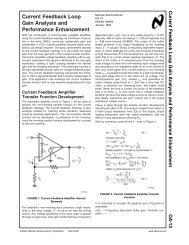
Lo<strong>op</strong> gain calculation
Basic usage: Non inverting amplifier<br />
G<br />
NINV<br />
dV<br />
OUT<br />
= =<br />
ZF<br />
lim GNINV<br />
= 1+<br />
Z →∞ Z<br />
( + Z )<br />
Z Z<br />
dV ZZ + Z Z + Z Z + Z Z<br />
IN G F B G B F G<br />
G<br />
Note that we have not introduced explicit frequency dependence!<br />
F<br />
G
Not common usage: Inverting<br />
G INV <br />
−ZZ F<br />
ZZ G Z B Z F Z B Z G Z F Z G<br />
lim<br />
Z →∞<br />
G<br />
INV<br />
=−<br />
Z<br />
Z<br />
F<br />
G
Gain calculation – frequency response<br />
G NINV <br />
ZZ F ZZ G<br />
ZZ G Z B Z F Z B Z G Z F Z G<br />
Z B h ib <br />
R B<br />
0 1<br />
1s 0 T<br />
1s T<br />
/11/ 0 <br />
Z T <br />
Z 0<br />
1s 1 1s 2 <br />
Transimpedance Z T<br />
has two poles: due to the impedance of the high Z node<br />
and also due to the current mirror delay<br />
Z B<br />
is the output impedance of the input buffer, small but not necessarily much<br />
smaller than Z G
Gain calculation – frequency response (2)<br />
G NINV <br />
ZZ F ZZ G<br />
ZZ G Z B Z F Z B Z G Z F Z G<br />
Z T <br />
Z 0<br />
1s 1 1s 2 <br />
Neglect Z B<br />
since it is much smaller than anything else. Then,<br />
Z<br />
NINV<br />
<br />
( + ) ⎛ ⎞ 1<br />
Z ZF ZG ZF<br />
= ⎜1+<br />
⎟<br />
ZZG + ZFZG ⎝ ZG ⎠1 + ZF<br />
/ Z<br />
<br />
Gain<br />
Bandwidth<br />
Observe that the gain and bandwidth have been decoupled.<br />
The bandwidth depends only on Z F<br />
(and Z B<br />
, really), while the<br />
gain depends on both Z F<br />
and Z G<br />
There is no magic involved. The CFOA is a dominant pole<br />
transimpedance amplifier, while the voltage and current buffers have<br />
poles at much higher frequencies.
Gain vs. frequency with R F (EL5166)
Gain vs frequency with R G (EL5166)<br />
Notice that despite what our approximations say the BW still depends on gain!
Gain bandwidth product – example
Frequency response of transimpedance<br />
The transimpedance has a dominant pole at 100kHz
Slew rate: VFOA vs CFOA<br />
• VFOA:<br />
• CFOA:<br />
IoutVFOA<br />
∝tanh<br />
( V<br />
+<br />
−V−<br />
)<br />
IoutCFOA<br />
∝ exp( Vy<br />
)<br />
dIout<br />
0<br />
dV<br />
→<br />
in<br />
dIout<br />
Iout<br />
dV →∝<br />
In the limit of large input voltages,<br />
in the VFOA:<br />
While in the CFOA we get:<br />
in<br />
4<br />
3.5<br />
3<br />
2.5<br />
2<br />
1.5<br />
1<br />
0.5<br />
0<br />
0 2 4 6 8 10<br />
The slew rate in the CFOA is power limited
Re-visit the non inverting amplifier<br />
V IN<br />
Y G<br />
+Y F<br />
Z<br />
V OUT<br />
Y F<br />
The CFOA is a transimpedance amplifier, i.e. equivalent to the block diagram<br />
The response is, in terms of the transimpedance Z is the usual FB expression:<br />
G<br />
NINV<br />
( + )<br />
Z Y Y Y Z<br />
= ⇒ lim GNINV<br />
= 1+ = 1+<br />
1+<br />
ZY Z →∞ Y Z<br />
G F G F<br />
F F G<br />
Notice that the lo<strong>op</strong> gain is ZZ F<br />
and that Z is typically second order beyond<br />
the first pole, so that, for a parallel RC in the <strong>feedback</strong> path we get a second<br />
order underdamped system.
Avoid capacitances!
Effect of Feedback capacitance<br />
INSTABILITY unless we introduce extra pole!
Input capacitance
Brute force compensation<br />
Low pass the non-inverting input to<br />
compensate for stray capacitance,<br />
i.e. brute force compensation
Effect of input (stray) capacitance
Output (load) capacitance
Applications I<br />
Inverting receiver<br />
Non-inverting receiver
Applications II<br />
Differential amplifier<br />
Differential line driver
Antenna circuits<br />
Coax cable driver<br />
Distribution amplifier
CFOA can be combined with other stages…<br />
With emitter follower<br />
With <strong>op</strong>-<strong>amps</strong>
Adjust BW by increasing inverting<br />
input impedance!<br />
Bandwidth and stability
Integrator<br />
Integrating capacitance NOT in<br />
<strong>feedback</strong> path.<br />
Capacitance must be lossy enough!
Implementation note:<br />
Supply bypassing is NOT <strong>op</strong>tional!