
Create successful ePaper yourself
Turn your PDF publications into a flip-book with our unique Google optimized e-Paper software.
XR<strong>16C864</strong> áç<br />
2.97V TO 5.5V QUAD <strong>UART</strong> WITH 128-BYTE FIFO REV. 2.0.1<br />
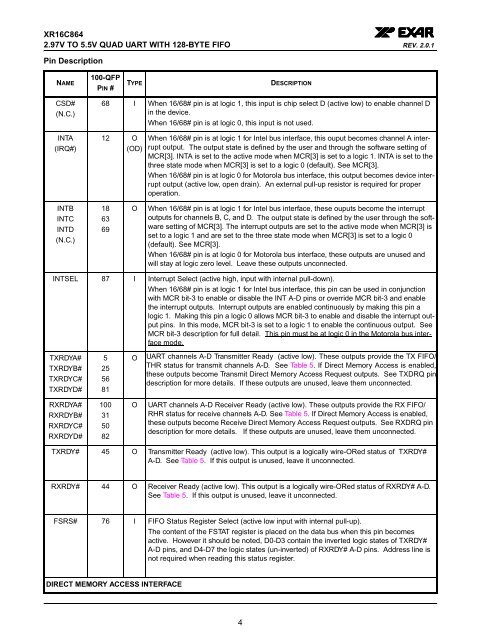
Pin Description<br />
NAME<br />
100-QFP<br />
PIN #<br />
TYPE<br />
DESCRIPTION<br />
CSD#<br />
(N.C.)<br />
INTA<br />
(IRQ#)<br />
68 I When 16/68# pin is at logic 1, this input is chip select D (active low) to enable channel D<br />
in the device.<br />
When 16/68# pin is at logic 0, this input is not used.<br />
12 O<br />
(OD)<br />
When 16/68# pin is at logic 1 for Intel bus interface, this ouput becomes channel A interrupt<br />
output. The output state is defined by the user and through the software setting of<br />
MCR[3]. INTA is set to the active mode when MCR[3] is set to a logic 1. INTA is set to the<br />
three state mode when MCR[3] is set to a logic 0 (default). See MCR[3].<br />
When 16/68# pin is at logic 0 for Motorola bus interface, this output becomes device interrupt<br />
output (active low, open drain). An external pull-up resistor is required for proper<br />
operation.<br />
INTB<br />
INTC<br />
INTD<br />
(N.C.)<br />
18<br />
63<br />
69<br />
O<br />
When 16/68# pin is at logic 1 for Intel bus interface, these ouputs become the interrupt<br />
outputs for channels B, C, and D. The output state is defined by the user through the software<br />
setting of MCR[3]. The interrupt outputs are set to the active mode when MCR[3] is<br />
set to a logic 1 and are set to the three state mode when MCR[3] is set to a logic 0<br />
(default). See MCR[3].<br />
When 16/68# pin is at logic 0 for Motorola bus interface, these outputs are unused and<br />
will stay at logic zero level. Leave these outputs unconnected.<br />
INTSEL 87 I Interrupt Select (active high, input with internal pull-down).<br />
When 16/68# pin is at logic 1 for Intel bus interface, this pin can be used in conjunction<br />
with MCR bit-3 to enable or disable the INT A-D pins or override MCR bit-3 and enable<br />
the interrupt outputs. Interrupt outputs are enabled continuously by making this pin a<br />
logic 1. Making this pin a logic 0 allows MCR bit-3 to enable and disable the interrupt output<br />
pins. In this mode, MCR bit-3 is set to a logic 1 to enable the continuous output. See<br />
MCR bit-3 description for full detail. This pin must be at logic 0 in the Motorola bus interface<br />
mode.<br />
TXRDYA#<br />
TXRDYB#<br />
TXRDYC#<br />
TXRDYD#<br />
RXRDYA#<br />
RXRDYB#<br />
RXRDYC#<br />
RXRDYD#<br />
5<br />
25<br />
56<br />
81<br />
O<br />
<strong>UART</strong> channels A-D Transmitter Ready (active low). These outputs provide the TX FIFO/<br />
THR status for transmit channels A-D. See Table 5. If Direct Memory Access is enabled,<br />
these outputs become Transmit Direct Memory Access Request outputs. See TXDRQ pin<br />
description for more details. If these outputs are unused, leave them unconnected.<br />
100<br />
31<br />
50<br />
82<br />
O<br />
<strong>UART</strong> channels A-D Receiver Ready (active low). These outputs provide the RX FIFO/<br />
RHR status for receive channels A-D. See Table 5. If Direct Memory Access is enabled,<br />
these outputs become Receive Direct Memory Access Request outputs. See RXDRQ pin<br />
description for more details. If these outputs are unused, leave them unconnected.<br />
TXRDY# 45 O Transmitter Ready (active low). This output is a logically wire-ORed status of TXRDY#<br />
A-D. See Table 5. If this output is unused, leave it unconnected.<br />
RXRDY# 44 O Receiver Ready (active low). This output is a logically wire-ORed status of RXRDY# A-D.<br />
See Table 5. If this output is unused, leave it unconnected.<br />
FSRS# 76 I FIFO Status Register Select (active low input with internal pull-up).<br />
The content of the FSTAT register is placed on the data bus when this pin becomes<br />
active. However it should be noted, D0-D3 contain the inverted logic states of TXRDY#<br />
A-D pins, and D4-D7 the logic states (un-inverted) of RXRDY# A-D pins. Address line is<br />
not required when reading this status register.<br />
DIRECT MEMORY ACCESS INTERFACE<br />
4