Vertical Vertical Circuits Circuits - Meptec
Vertical Vertical Circuits Circuits - Meptec
Vertical Vertical Circuits Circuits - Meptec

Create successful ePaper yourself
Turn your PDF publications into a flip-book with our unique Google optimized e-Paper software.
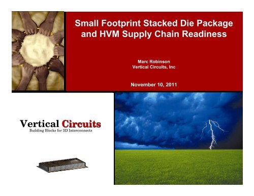
Small Footprint Stacked Die Package<br />
and HVM Supply Chain Readiness<br />
Marc Robinson<br />
<strong>Vertical</strong> <strong>Circuits</strong>, Inc<br />
November 10, 2011<br />
<strong>Vertical</strong> <strong>Circuits</strong><br />
Building Blocks for 3D Interconnects
Infrastructure Readiness<br />
Multi-Die Packaging HVM<br />
•Market<br />
• Process<br />
• Equipment<br />
• Materials<br />
• Importance of KGD for HVM<br />
2
<strong>Vertical</strong> <strong>Circuits</strong><br />
A leading developer of low cost semiconductor<br />
device stacking and interconnect technology<br />
enabling the thinnest, smallest and highest<br />
performance form factor for 3D IC components<br />
3
<strong>Vertical</strong> <strong>Circuits</strong> – A Brief “History”<br />
Confidential<br />
• A developer of low cost semiconductor device stacking and<br />
interconnect technology enabling the thinnest, smallest and<br />
highest performance form factor for 3D IC components:<br />
•1989: Memory Wafer Stacks with TSV for SSD<br />
•1996: 32 Die DRAM Stacks with redundancy for<br />
solid state recorders<br />
•1998: Low cost mixed die flip chip package<br />
•2001: 2 & 4 DRAM stacked die BGA components<br />
for servers<br />
•2007: Low cost HVM process for 8 and 16 die<br />
flash components<br />
•2010: Low cost HVM process for mixed-die<br />
stacks<br />
4
Core Technology<br />
Confidential<br />
DIELECTRIC COATINGS<br />
Protective 5-Sided Conformal Dielectric Coating<br />
VERTICAL CONDUCTORS (VIP TM )<br />
3D Conductive Polymer Interconnects<br />
8 Die NAND – Wire Bond 8-Die NAND – <strong>Vertical</strong> <strong>Circuits</strong><br />
Smaller Size<br />
Increased Perf<br />
Higher Yield<br />
Lower Cost<br />
5
VCI Value Proposition<br />
Confidential<br />
VCI Technology Enables Smaller, Denser Packaging Solutions<br />
<strong>Vertical</strong> Structure - cost effective & reliable 3D structure<br />
6
VCI Value Proposition<br />
Confidential<br />
• Performance: Significant lower inductance (0.09nH vs. 1.5nH) in a<br />
8H+ flash stack structure resulting in improve signal integrity<br />
• Application: Higher flash speed required in new flash standard such as USB3.0<br />
or SATA6.0<br />
• Cost: based on our cost analysis, VCI assembly cost is 20-30%<br />
lower.<br />
• For example: a 8H uSD card ($0.8 vs. $1.09)<br />
• Yield: Improve test yield (reduce micro cracks induces in assembly process)<br />
• Density: through VCI technology, flash vendors can place larger<br />
monolithic flash dies into a standard form factor resulting in 2X<br />
density.<br />
• Simplicity: Gang assembly process simplify high density, tight form<br />
factor design resulting in higher overall yield and reducing assembly<br />
cycle time<br />
7
<strong>Vertical</strong> <strong>Circuits</strong> Business Model<br />
Confidential<br />
• Commercialize and license IP to IDM’s, OEM’s and high volume IC<br />
assembly houses<br />
• Drive vertical interconnect IP development roadmap – create a new<br />
industry standard<br />
• Offer low volume prototyping from the US and high volume<br />
manufacturing services through out-sourced assembly partnerships<br />
8
Confidential<br />
Customer Applications<br />
9
VCI Technology Applications – “Smart” Devices<br />
Confidential<br />
VCI 3D Values:<br />
• Lower Cost<br />
• Higher Performance<br />
• Innovative features<br />
• Longer battery life<br />
• Smaller size<br />
• Lighter weight<br />
• Shorter time to market<br />
10
Mobile Product<br />
Confidential<br />
<strong>Vertical</strong> Interconnect Pillar (ViP)<br />
mDDR<br />
mDDR<br />
Processor<br />
mDDR<br />
Processor<br />
<strong>Vertical</strong> Interconnect<br />
Substrate<br />
11
VCI Enabled Solid State Drive<br />
Confidential<br />
Continued miniaturization<br />
3.5” 128GB<br />
VCI Stacked Die<br />
WLCSP Engineering SSD<br />
12<br />
1.8” Hybrid Drive, 32GB
64GB uSD (Next Generation Design)<br />
Confidential<br />
13
SSD Market Focus – mSATA<br />
Confidential<br />
• SSD Key Growth Area – mSATA (a small flash module for tablet and<br />
Ultra-Portable)<br />
Apple<br />
Asus<br />
Samsung<br />
Lenovo<br />
14
VCI Markets – Solid States Drives<br />
Confidential<br />
• Reference Gartner/iSuppli reports<br />
• SSD adoption continues to grow with projected ~ 60 to 90M SSD in 2012<br />
• SSD units CAGR is ~85%<br />
• In 2012, ~18% of global PC will have SSD installed at POS<br />
• VCI performance + density solution provide unique value to SSD OEMs<br />
15
WLCSP VIP<br />
Confidential<br />
WLCSP ViP Edge<br />
WLCSP ViP Foot<br />
16
Stackable Leadframe Package<br />
Confidential<br />
17
Broad Market Applications<br />
Confidential<br />
• Vast market potential through broad 3D application<br />
- Smallest, highest density memory – 8H vertical stack WLCSP<br />
- Low power, high speed CPU – ASIC SiP (system in package)<br />
- WiFi / Analog / Bluetooth module – package stack<br />
-<br />
- High density sensor / ASIC MEMS – fingerprint, CMOS sensor<br />
18
Confidential<br />
Technology Summary<br />
19
DAG VERTICAL STACK PROCESS FLOW<br />
Confidential<br />
WAFER<br />
DIELECTRIC<br />
COAT<br />
WAFER<br />
LASER<br />
ABLATION<br />
DAF LAMINATION,<br />
WAFER MOUNT &<br />
BG TAPE REMOVAL<br />
WAFER BACKGRIND<br />
& POLISH<br />
BG TAPE<br />
LAMINATION<br />
WAFER<br />
SCREENPRINT<br />
next page<br />
20
DAG VERTICAL STACK PROCESS FLOW<br />
Confidential<br />
WAFER<br />
DAF<br />
TAPE<br />
SINGLE-<br />
CHANNEL<br />
SCRIBE<br />
(HALF-CUT<br />
DAF)<br />
WAFER<br />
DAF<br />
TAPE<br />
2 ND COAT DICING<br />
WAFER<br />
DAF<br />
TAPE<br />
SUBSTRATE<br />
VIP & CURE<br />
SUBSTRATE<br />
DIE STACK<br />
WAFER<br />
DAF<br />
TAPE<br />
CODE LASE<br />
next page<br />
21
DAG VERTICAL STACK PROCESS FLOW<br />
Confidential<br />
MOLD & CURE<br />
MARK,<br />
SINGULATION<br />
& TEST<br />
22
VCI Material Selection:<br />
Fine Nano Ag Particle Inks<br />
Confidential<br />
Fine line dispense (
Equipment / Material Support<br />
HVM Equipment Partnership<br />
‣Creation of HVM system geared toward inkjet printing with high output.<br />
‣3 separate systems enabling parallel development efforts:<br />
a.Software<br />
b.Hardware<br />
c.Peripherals<br />
d.Printing capability.<br />
‣Validation of printer settings supplied by VCI and transfer to Q-Class print head.<br />
Confidential<br />
24<br />
Scanned_printing.MOV
Stacking Structures<br />
Confidential<br />
Staggered Edges<br />
Aligned Edges<br />
Offset Edges<br />
25
<strong>Vertical</strong> Interconnect Structures<br />
Confidential<br />
100um Conformal Conductors<br />
at 200um Pitch on 8-die Stack<br />
16-die NAND Flash<br />
Terraced Stack<br />
26<br />
30um Conductors at 200um<br />
Pitch on 4-die Stack<br />
Arrow Stack with<br />
Conformal Interconnect
VCI Reliability<br />
Confidential<br />
VCI DRAM (BGA)<br />
‐Server Level<br />
Reliability‐<br />
VCI FLASH (µSD) VCI FLASH (LGA) VCI SiP (BGA)<br />
Moisture Resist<br />
Test:<br />
JEDEC Level 3<br />
@260°C<br />
JEDEC Level 3<br />
@260°C<br />
JEDEC Level 3<br />
@260°C<br />
JEDEC Level 3<br />
@260°C<br />
Biased‐HAST:<br />
Bias 3.6V, 130°C,<br />
85% RH, 144 hours<br />
Bias 3.6V, 130°C,<br />
85% RH, 96 hours<br />
Bias 3.6V, 130°C,<br />
85% RH, 96 hours<br />
Bias 3.6V, 130°C,<br />
85% RH, 96 hours<br />
Autoclave/PCT:<br />
Unbiased, 121°C,<br />
2atm, 100%RH, 96<br />
hours<br />
NO<br />
Unbiased, 121°C,<br />
2atm, 100%RH,<br />
96 hours<br />
Unbiased, 121°C,<br />
2atm, 100%RH, 96<br />
hours<br />
High Temp Storage:<br />
150°C,<br />
1000 hours<br />
150°C,<br />
1000 hours<br />
150°C,<br />
1000 hours<br />
150°C,<br />
1000 hours<br />
Temp Cycle:<br />
‐55/+125°C,<br />
1000 cycles (B)<br />
‐55/+125°C,<br />
1000 cycles (B)<br />
‐55/+125°C,<br />
1000 cycles (B)<br />
‐55/+125°C,<br />
1000 cycles (B)<br />
Card Tests:<br />
(DBT/Insert/Salt)<br />
N/A SDI Spec. N/A N/A<br />
27<br />
• DDR-SDRAM parts tested at Server Level Reliability Specifications.<br />
• Flash products are simpler and larger, meeting the above specifications for cards and components.
Technology Roadmap<br />
Confidential<br />
2010 2011<br />
Trace<br />
1.0mm<br />
2011 key focus:<br />
•
KGD – A Key Link in The Supply Chain<br />
Confidential<br />
• KGD is an enabling building block in the HVM supply<br />
chain for multi chip packaging.<br />
• Is the supply chain getting ahead of KGD?<br />
• KGD capabilities?<br />
• KGD costs?<br />
• Equipment?<br />
• Operational?<br />
• Testing does not add value, but is driven by supply<br />
chain segmentation.<br />
• If KGD implementation is too expensive, will other solutions<br />
prevail? (eg. Self repair, redundancy)<br />
• Test cost must be less than yield cost!<br />
29
At What Level in the Heirarchy?<br />
Confidential<br />
• Interconnect<br />
• Functional Blocks<br />
• System<br />
• Testing Functionality or Construction?<br />
• Encouraging standards between die suppliers<br />
30
Confidential<br />
Summary<br />
31
Summary<br />
Confidential<br />
• The Market is Ready!<br />
• Market applications are demanding multi-die solutions for form factor,<br />
functionality, and cost. (Homogeneous & Heterogeneous)<br />
• Processes are Ready!<br />
• Multiple solutions to multi die packaging<br />
• For VCI, Simple Gang/Parallel processing approach facilitates a simple<br />
line with reduced logistics and operations, and hence lower cost.<br />
• Manufacturing Equipment is Ready Some of the Approaches<br />
• Materials Suppliers are Ready for Some of the Approaches<br />
• For VCI Conductive Polymers Allow A Near-TSV Edge-Conductor<br />
Solution Enabling Chip-Scale Form-Factor Die and Package Stacking.<br />
• Is KGD ready?<br />
• Supply chain benefits from KGD infrastructure: Yield & Cost<br />
• KGD can be an enabler, or an obstacle.<br />
• If it remains an obstacle, other solutions will prevail.<br />
32
Confidential<br />
THANK YOU<br />
marc.robinson@verticalcircuits.com<br />
33