The Miller Theorem and the Frequency Response of the Common ...
The Miller Theorem and the Frequency Response of the Common ...
The Miller Theorem and the Frequency Response of the Common ...
Create successful ePaper yourself
Turn your PDF publications into a flip-book with our unique Google optimized e-Paper software.
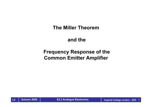
<strong>The</strong> <strong>Miller</strong> <strong>The</strong>orem<br />
<strong>and</strong> <strong>the</strong><br />
<strong>Frequency</strong> <strong>Response</strong> <strong>of</strong> <strong>the</strong><br />
<strong>Common</strong> Emitter Amplifier<br />
L2 Autumn 2009 E2.2 Analogue Electronics<br />
Imperial College London – EEE 1
A useful approximation: <strong>The</strong> <strong>Miller</strong> <strong>The</strong>orem<br />
• Consider a shunt admittance connected between <strong>the</strong> input <strong>and</strong> output <strong>of</strong> an<br />
inverting voltage amplifier <strong>of</strong> gain G.<br />
Y<br />
In Out<br />
V V In<br />
I F<br />
-I F Out<br />
-G<br />
-G<br />
I in<br />
I (1+G)Y<br />
1 I 2 I (1+1/G)Y<br />
out<br />
• Assuming that Y does not affect <strong>the</strong> gain, KCL at <strong>the</strong> input says that:<br />
( ) ⎡⎣( 1 ) ⎤⎦<br />
( ) ⎡( 1 1/ )<br />
i = i + i = i + v − v Y = i + + G Y v<br />
in 1 F 1 in out 1<br />
in<br />
i = i − i = i − v − v Y = i + ⎣ + G Y⎤⎦<br />
v<br />
out 2 F 2 in out 2<br />
out<br />
• This is <strong>the</strong> same current as we would get if we connected Y(1+G) in parallel to<br />
<strong>the</strong> input <strong>and</strong> Y(1+1/G) in parallel to <strong>the</strong> output (on <strong>the</strong> right)<br />
• Note that this is an approximation; Y always changes <strong>the</strong> gain,<br />
unless Z out<br />
// Z L<br />
= 0. None<strong>the</strong>less, very <strong>of</strong>ten it is a good approximation.<br />
L2 Autumn 2009 E2.2 Analogue Electronics<br />
Imperial College London – EEE 2
An application <strong>of</strong> <strong>the</strong> <strong>Miller</strong> <strong>the</strong>orem<br />
Input impedance <strong>of</strong> <strong>the</strong> inverting amplifier (if op-amp has zero Y in ):<br />
R1<br />
R2<br />
v in 2<br />
G V out<br />
Zin<br />
= R1<br />
+<br />
( 1+<br />
G)<br />
R<br />
We can even use <strong>the</strong> <strong>Miller</strong> <strong>the</strong>orem to calculate <strong>the</strong> gain <strong>of</strong> this circuit<br />
for finite op-amp gain G:<br />
( G )<br />
/( 1)<br />
v R / + 1)<br />
out<br />
−GR −R<br />
Av<br />
= =− G = , lim A =<br />
v R R G RG R R R<br />
in<br />
2 2 2<br />
v<br />
1+ 2<br />
+<br />
1<br />
+ G→∞<br />
1+<br />
2 1<br />
This is <strong>the</strong> correct answer for <strong>the</strong> closed loop gain as we shall later see!<br />
SF1.6p34<br />
L2 Autumn 2009 E2.2 Analogue Electronics<br />
Imperial College London – EEE 3
<strong>The</strong> small signal model <strong>the</strong> <strong>of</strong> BJT<br />
• <strong>The</strong> model below is useful to frequencies <strong>of</strong> up to 100s <strong>of</strong> MHz<br />
• <strong>The</strong> model is strictly valid for B-E voltage variations smaller than V T<br />
=25mV.<br />
• To analyse a circuit:<br />
– Each transistor in a circuit is replaced by this model<br />
– <strong>The</strong> “base spreading resistance” R BB<br />
is lumped with <strong>the</strong> <strong>the</strong>venin<br />
impedance <strong>of</strong> <strong>the</strong> signal source. It is not shown explicitly in <strong>the</strong>se<br />
notes.<br />
What does R BB<br />
do:<br />
• R BB<br />
is responsible for most <strong>of</strong> <strong>the</strong> noise <strong>of</strong> transistor amplifiers<br />
• R BB<br />
is responsible for <strong>the</strong> power gain rolling-<strong>of</strong>f at high frequencies<br />
• R BB<br />
is <strong>of</strong>ten ignored at “low” (f < MHz) frequencies<br />
L2 Autumn 2009 E2.2 Analogue Electronics<br />
Imperial College London – EEE 4
BJT model: impedances <strong>and</strong> transconductance<br />
• <strong>The</strong> large signal BJT equation gives <strong>the</strong> transconductance:<br />
Vbe ( / V<br />
⎛ V ⎞<br />
th CE Vbe )<br />
/ Vth<br />
IC<br />
= I0 e − 1 ⎜1+<br />
⎟<br />
I0e<br />
⎝ VA<br />
⎠<br />
kT<br />
B<br />
Vth<br />
= 26 mV at room temperature<br />
e<br />
∂IC<br />
IC<br />
gm<br />
= ∂ V V<br />
be<br />
th<br />
• However, since I E<br />
=(1+1/β)I C<br />
,<br />
∂VBE<br />
Rπ = = βV / I = β / g<br />
∂I<br />
T C m<br />
• Same equation gives output conductance:<br />
G<br />
CE<br />
B<br />
∂I<br />
= R = =<br />
C C<br />
1/<br />
CE<br />
∂VCE<br />
VA<br />
I<br />
L2 Autumn 2009 E2.2 Analogue Electronics<br />
Imperial College London – EEE 5
BJT model Capacitances<br />
• BC junction is reverse biased:<br />
– depletion capacitance<br />
– overlap capacitance<br />
• BE junction is forward biased:<br />
– depletion capacitance<br />
– storage (diffusion capacitance)<br />
– overlap capacitance<br />
• CE capacitance is small<br />
– overlap capacitance<br />
• Fringing/Overlap capacitances:<br />
C = C + C<br />
BC BC 0 j<br />
C = C + C + C<br />
C<br />
BE BE0<br />
j D<br />
<br />
C<br />
CE CE0<br />
C , C , C<br />
BC0 BE0 CE0<br />
• Junction capacitance:<br />
– Reverse biased diode<br />
– M=1/2-1/3, from doping<br />
– Φ approx 0.8V<br />
– M, Φ usually determined from two<br />
bias points<br />
C<br />
j<br />
0<br />
=<br />
M<br />
⎛ VBE<br />
⎞<br />
⎜1−<br />
⎝<br />
C<br />
Φ<br />
⎟<br />
⎠<br />
• Diffusion capacitance<br />
– from transit time<br />
C = g τ , τ = 1/ 2 π f<br />
D m T T T<br />
L2 Autumn 2009 E2.2 Analogue Electronics<br />
Imperial College London – EEE 6
An important figure <strong>of</strong> merit:<br />
<strong>the</strong> BJT Current gain <strong>and</strong> <strong>the</strong> transit frequency f T<br />
<strong>The</strong> transistor is connected as a current amplifier:<br />
• Driven by a current source<br />
• Driving a current meter<br />
f T<br />
is <strong>the</strong> frequency at which <strong>the</strong> current gain drops to unity.<br />
f T<br />
is usually specified by <strong>the</strong> transistor manufacturer as a figure <strong>of</strong> merit.<br />
f T<br />
is a rough estimate <strong>of</strong> <strong>the</strong> highest frequency at which <strong>the</strong> transistor<br />
can be used as an amplifier. Typically fT / 10 is this highest frequency.<br />
L2 Autumn 2009 E2.2 Analogue Electronics<br />
Imperial College London – EEE 7
An important figure <strong>of</strong> merit:<br />
<strong>the</strong> BJT Current gain <strong>and</strong> <strong>the</strong> transit frequency f T<br />
( ( ) 1/<br />
π )<br />
iB = vBE s CBE + CBC<br />
+ R ⎫⎪ ⎬ ⇒<br />
iC = gmvBE<br />
⎪⎭<br />
i g g R<br />
β<br />
= " h " = = =<br />
i s C C R sR C C s f<br />
C m m π<br />
0<br />
fe<br />
B ( BE<br />
+<br />
BC) + 1/<br />
π<br />
1+ π ( BE<br />
+<br />
BC)<br />
1 + β0<br />
/2π<br />
T<br />
β<br />
g g<br />
β<br />
where fT<br />
= = , since: R =<br />
2 πR C + C π C + C πC g<br />
<strong>the</strong> current gain is<br />
π<br />
0 m<br />
m<br />
0<br />
π<br />
BE BC<br />
2<br />
BE BC<br />
2<br />
BE m<br />
( ) ( )<br />
h<br />
fe<br />
( f )<br />
β<br />
= ⇒<br />
1+<br />
j f f<br />
lim<br />
0<br />
β f > f<br />
0 T<br />
/ T<br />
/ β<br />
0<br />
h<br />
fe<br />
fT<br />
= with fT<br />
=<br />
f<br />
1<br />
2πτ<br />
T<br />
f T<br />
allows <strong>the</strong> easy calculation <strong>of</strong> C BE<br />
+ C BC<br />
since g m<br />
only depends on <strong>the</strong><br />
collector bias current! Note that C BE<br />
>>C BC<br />
so knowing f T<br />
defines C BE<br />
L2 Autumn 2009 E2.2 Analogue Electronics<br />
Imperial College London – EEE 8
Load<br />
<strong>The</strong> <strong>Common</strong> Emitter amplifier<br />
Source<br />
Amplifier<br />
Model parameters:<br />
⎧ ∂IC<br />
IC<br />
⎪gm<br />
= =<br />
⎪ ∂VBE<br />
VT<br />
−1 −1<br />
−1<br />
⎪ ⎛ ∂I<br />
⎞ ⎛∂<br />
( IC<br />
/ β<br />
B<br />
) ⎞ ⎛ ∂I<br />
⎞<br />
C<br />
β<br />
⎨Rπ<br />
= ⎜ ⎟ = ⎜ ⎟ = β ⎜ ⎟ =<br />
⎪ ⎝∂VBE ⎠ ⎝ ∂VBE ⎠ ⎝∂VBE ⎠ gm<br />
⎪<br />
−1<br />
⎪ ⎛ ∂I<br />
⎞<br />
C<br />
VA<br />
RCE<br />
= ⎜ ⎟ <br />
⎪<br />
⎩ ⎝∂VCE<br />
⎠ IC<br />
V = kT / q = 25mV at 290K=17C<br />
T<br />
L2 Autumn 2009 E2.2 Analogue Electronics<br />
Imperial College London – EEE 9
<strong>The</strong> <strong>Common</strong> Emitter amplifier (2)<br />
Combine , , into a <strong>The</strong>venin circuit:<br />
S<br />
R<br />
= =<br />
S<br />
π<br />
S<br />
VS1<br />
VS<br />
R<br />
π<br />
+ Z<br />
S<br />
1+<br />
Z<br />
S Y<br />
in<br />
RZ<br />
π S<br />
ZS<br />
RS1<br />
= Rπ<br />
// ZS<br />
= =<br />
R + Z 1+<br />
Z Y<br />
π<br />
V<br />
S S in<br />
V Z R π<br />
2<br />
RCEZL ZL<br />
Consider RCE <strong>and</strong> ZL toge<strong>the</strong>r: R = RCE / / ZL<br />
= =<br />
R + Z 1+<br />
Z Y<br />
<strong>and</strong> note that<br />
Z = R + R<br />
S S BB<br />
CE L L out<br />
L2 Autumn 2009 E2.2 Analogue Electronics<br />
Imperial College London – EEE 10
<strong>The</strong> <strong>Common</strong> Emitter amplifier (3)<br />
Gain:<br />
A<br />
v<br />
v ∂V<br />
V 1 −g Z<br />
= ≡ =− g R =<br />
v V V RY Z Y<br />
out 2 s1<br />
m L<br />
m 2<br />
s<br />
∂<br />
s s<br />
+<br />
s in<br />
+<br />
L out<br />
If Y in<br />
= 0 <strong>and</strong> Y out<br />
= 0 this is <strong>the</strong> familiar:<br />
A<br />
v<br />
= ≡−g Z<br />
out<br />
v m L<br />
vs<br />
( 1 ) ( 1 )<br />
Note that lowercase letters represent small signal variations, i.e. differentials<br />
L2 Autumn 2009 E2.2 Analogue Electronics<br />
Imperial College London – EEE 11
<strong>The</strong> <strong>Common</strong> Emitter amplifier (4):<br />
Input <strong>and</strong> output impedance<br />
Input Impedance:<br />
Output Impedance:<br />
Z<br />
Z<br />
in<br />
out<br />
∂V<br />
∂I<br />
−1<br />
BE<br />
B<br />
= = =<br />
B<br />
∂V<br />
∂I<br />
BE<br />
−1<br />
C<br />
C<br />
= = =<br />
out<br />
⎛ ∂I<br />
⎜<br />
⎝∂V<br />
⎛ ∂I<br />
⎜<br />
⎝∂V<br />
CE<br />
⎞<br />
⎟<br />
⎠<br />
⎞<br />
⎟<br />
⎠<br />
R<br />
π<br />
R<br />
CE<br />
L2 Autumn 2009 E2.2 Analogue Electronics<br />
Imperial College London – EEE 12
<strong>Frequency</strong> response <strong>of</strong><br />
<strong>the</strong> <strong>Common</strong> Emitter amplifier<br />
If we momentarily neglect C BC this would be <strong>the</strong> same as before but with:<br />
Input Impedance:<br />
Output Impedance:<br />
We still have:<br />
A<br />
V<br />
1<br />
Rπ<br />
Zin<br />
= = Rπ<br />
// CBE<br />
=<br />
Y 1 + jωC R<br />
in<br />
1<br />
RCE<br />
Zout = = RCE // CCE<br />
=<br />
Y 1 + jωC R<br />
vout 1 −gmZL<br />
v<br />
= =<br />
<strong>and</strong> = G =<br />
v ( 1+ RY ) ( 1+<br />
Z Y ) v<br />
BE<br />
out CE CE<br />
s s in L out<br />
π<br />
−g Z<br />
out m L<br />
( 1+<br />
Z Y )<br />
B L out<br />
L2 Autumn 2009 E2.2 Analogue Electronics<br />
Imperial College London – EEE 13
Dealing with C BC<br />
I CBC<br />
In <strong>the</strong> absence <strong>of</strong> C BC<br />
we know that:<br />
<strong>the</strong> current through C BC<br />
is:<br />
v<br />
v<br />
= G =<br />
−g Z<br />
out m L<br />
( 1+<br />
Z Y )<br />
B L out<br />
( ) ( 1 ) ( 1/ 1)<br />
I = jωC V − V = jωC − G V = jωC G−<br />
V<br />
CBC BC B C BC B BC C<br />
We can account for C BC<br />
by introducing an additional input “<strong>Miller</strong>” admittance:<br />
Min ,<br />
ω<br />
BC<br />
1<br />
( )<br />
Y = j C −G<br />
<strong>and</strong> an additional output “<strong>Miller</strong>” admittance:<br />
( )<br />
YMout<br />
,<br />
= jωCBC<br />
1−1/<br />
G<br />
L2 Autumn 2009 E2.2 Analogue Electronics<br />
Imperial College London – EEE 14
<strong>Frequency</strong> response <strong>of</strong> <strong>the</strong> CE amplifier<br />
V S1<br />
<strong>and</strong> R S1<br />
is <strong>the</strong> Τhevenin equivalent <strong>of</strong> R S<br />
V S<br />
<strong>and</strong> R π<br />
Use <strong>the</strong> <strong>Miller</strong> <strong>The</strong>orem to get:<br />
( ) ( ) ( )<br />
with C = C + 1+ G C 1 + G C <strong>and</strong> C = C + 1+<br />
1/ G C C<br />
2 BE BC BC 3 CE BC BC<br />
<strong>The</strong> low requency gain from V1 to V2 is: G = −gmR2<br />
−gmZL<br />
L2 Autumn 2009 E2.2 Analogue Electronics<br />
Imperial College London – EEE 15
<strong>Frequency</strong> response <strong>of</strong> <strong>the</strong> CE amplifier (2)<br />
<strong>the</strong> gain <strong>of</strong> this amplifier is:<br />
dV2 −gm<br />
R2<br />
G<br />
= =<br />
dVS1 1+ sRS1C2 1+ sRC<br />
2 3 ( 1+ sRS1C2)( 1+<br />
sRC<br />
2 3)<br />
<br />
input pole<br />
If <strong>the</strong> gain is large <strong>the</strong> input pole can be at a much lower frequency than <strong>the</strong> output pole:<br />
τ = R C = R // R C + 1+ G C R 1 + G C since R R<br />
τ<br />
if τ<br />
in<br />
> τ<br />
out <strong>The</strong> gain-b<strong>and</strong>width product <strong>of</strong> this amplifier is:<br />
G = gmR2<br />
gmZL<br />
⎫<br />
⎪ gmR2<br />
G<br />
1<br />
1 1 ⎬ ⇒ GBW = . lim GBW <br />
.<br />
BW = <br />
2πRC G →∞<br />
S 2<br />
2 πRC S BC(1 + G) 2πRC<br />
S BC<br />
2πRS1C2 2πRSC<br />
⎪<br />
2⎭<br />
This is independent <strong>of</strong> G!<br />
<strong>The</strong> tiny C <strong>and</strong> <strong>the</strong> s ource impedance can define <strong>the</strong> gain-b<strong>and</strong>width product <strong>of</strong> <strong>the</strong> CE amp.<br />
BC<br />
( π ) ( )<br />
( ( ) )( )<br />
This suggests that feedback is at work!<br />
Note that <strong>the</strong> input pole will be at a lower frequency than <strong>the</strong> output pole if<br />
> ⇒ > ⇒ = / > 1<br />
G RS1 R2 gmRS1R2 R2<br />
gmRS β RS<br />
R π<br />
( ) ( ) ( π )<br />
IN S1 2<br />
S BE BC S BC S<br />
= RC = C 1+ 1/ G + C R // Z C Z (since C C<br />
)<br />
OUT 2 3 BC CE CE L BC L BC CE<br />
output pole<br />
L2 Autumn 2009 E2.2 Analogue Electronics<br />
Imperial College London – EEE 16
Importance <strong>of</strong> <strong>the</strong> gain-b<strong>and</strong>width product<br />
<strong>the</strong> gain <strong>of</strong> <strong>the</strong> CE amplifier is:<br />
dV2 −gm<br />
R2<br />
G<br />
= =<br />
dVS1 1+ sRS1C2 1+ sRC<br />
2 3 ( 1+ sRS1C2)( 1+<br />
sRC<br />
2 3)<br />
<br />
input pole<br />
output pole<br />
One <strong>of</strong> <strong>the</strong> two pole frequencies is usually much lower than <strong>the</strong> o<strong>the</strong>r.<br />
We <strong>the</strong>n say that we have a dominant pole amplifier whose frequency response is:<br />
A<br />
v<br />
G G<br />
1+ sτ<br />
1+<br />
jωτ<br />
0 0<br />
( s) = =<br />
for a DC gain G 0<br />
<strong>and</strong> a b<strong>and</strong>width ω = 1/<br />
We have already seen that in <strong>the</strong> limit <strong>of</strong> large G 0<br />
<strong>the</strong> Gain-B<strong>and</strong>width product:<br />
G = G = G<br />
is independent <strong>of</strong> <strong>the</strong> amplifier gain.<br />
B<br />
0ω<br />
/<br />
B 0<br />
We will see later in <strong>the</strong> course that this is a very general result which applies to<br />
all one pole feedback amplifiers regardless <strong>of</strong> how <strong>the</strong>y are constructed.<br />
τ<br />
B<br />
τ<br />
L2 Autumn 2009 E2.2 Analogue Electronics<br />
Imperial College London – EEE 17


