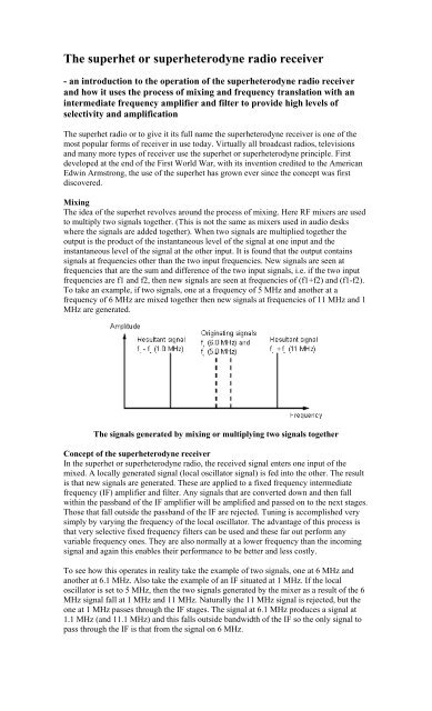
The superhet or superheterodyne radio receiver
The superhet or superheterodyne radio receiver
The superhet or superheterodyne radio receiver

You also want an ePaper? Increase the reach of your titles
YUMPU automatically turns print PDFs into web optimized ePapers that Google loves.
<strong>The</strong> <strong>superhet</strong> <strong>or</strong> <strong>superhet</strong>erodyne <strong>radio</strong> <strong>receiver</strong><br />
- an introduction to the operation of the <strong>superhet</strong>erodyne <strong>radio</strong> <strong>receiver</strong><br />
and how it uses the process of mixing and frequency translation with an<br />
intermediate frequency amplifier and filter to provide high levels of<br />
selectivity and amplification<br />
<strong>The</strong> <strong>superhet</strong> <strong>radio</strong> <strong>or</strong> to give it its full name the <strong>superhet</strong>erodyne <strong>receiver</strong> is one of the<br />
most popular f<strong>or</strong>ms of <strong>receiver</strong> in use today. Virtually all broadcast <strong>radio</strong>s, televisions<br />
and many m<strong>or</strong>e types of <strong>receiver</strong> use the <strong>superhet</strong> <strong>or</strong> <strong>superhet</strong>erodyne principle. First<br />
developed at the end of the First W<strong>or</strong>ld War, with its invention credited to the American<br />
Edwin Armstrong, the use of the <strong>superhet</strong> has grown ever since the concept was first<br />
discovered.<br />
Mixing<br />
<strong>The</strong> idea of the <strong>superhet</strong> revolves around the process of mixing. Here RF mixers are used<br />
to multiply two signals together. (This is not the same as mixers used in audio desks<br />
where the signals are added together). When two signals are multiplied together the<br />
output is the product of the instantaneous level of the signal at one input and the<br />
instantaneous level of the signal at the other input. It is found that the output contains<br />
signals at frequencies other than the two input frequencies. New signals are seen at<br />
frequencies that are the sum and difference of the two input signals, i.e. if the two input<br />
frequencies are f1 and f2, then new signals are seen at frequencies of (f1+f2) and (f1-f2).<br />
To take an example, if two signals, one at a frequency of 5 MHz and another at a<br />
frequency of 6 MHz are mixed together then new signals at frequencies of 11 MHz and 1<br />
MHz are generated.<br />
<strong>The</strong> signals generated by mixing <strong>or</strong> multiplying two signals together<br />
Concept of the <strong>superhet</strong>erodyne <strong>receiver</strong><br />
In the <strong>superhet</strong> <strong>or</strong> <strong>superhet</strong>erodyne <strong>radio</strong>, the received signal enters one input of the<br />
mixed. A locally generated signal (local oscillat<strong>or</strong> signal) is fed into the other. <strong>The</strong> result<br />
is that new signals are generated. <strong>The</strong>se are applied to a fixed frequency intermediate<br />
frequency (IF) amplifier and filter. Any signals that are converted down and then fall<br />
within the passband of the IF amplifier will be amplified and passed on to the next stages.<br />
Those that fall outside the passband of the IF are rejected. Tuning is accomplished very<br />
simply by varying the frequency of the local oscillat<strong>or</strong>. <strong>The</strong> advantage of this process is<br />
that very selective fixed frequency filters can be used and these far out perf<strong>or</strong>m any<br />
variable frequency ones. <strong>The</strong>y are also n<strong>or</strong>mally at a lower frequency than the incoming<br />
signal and again this enables their perf<strong>or</strong>mance to be better and less costly.<br />
To see how this operates in reality take the example of two signals, one at 6 MHz and<br />
another at 6.1 MHz. Also take the example of an IF situated at 1 MHz. If the local<br />
oscillat<strong>or</strong> is set to 5 MHz, then the two signals generated by the mixer as a result of the 6<br />
MHz signal fall at 1 MHz and 11 MHz. Naturally the 11 MHz signal is rejected, but the<br />
one at 1 MHz passes through the IF stages. <strong>The</strong> signal at 6.1 MHz produces a signal at<br />
1.1 MHz (and 11.1 MHz) and this falls outside bandwidth of the IF so the only signal to<br />
pass through the IF is that from the signal on 6 MHz.
<strong>The</strong> basic concept of the <strong>superhet</strong> <strong>radio</strong><br />
If the local oscillat<strong>or</strong> frequency is moved up by 0.1 MHz to 5.1 MHz then the signal at<br />
6.1 MHz will give rise to a signal at 1 MHz and this will pass through the IF. <strong>The</strong> signal<br />
at 6 MHz will give rise to a signal of 0.9 MHz at the IF and will be rejected. In this way<br />
the <strong>receiver</strong> acts as a variable frequency filter, and tuning is accomplished.<br />
Images<br />
<strong>The</strong> basic concept of the <strong>superhet</strong>erodyne <strong>receiver</strong> appears to be fine, but there is a<br />
problem. <strong>The</strong>re are two signals that can enter the IF. With the local oscillat<strong>or</strong> set to 5<br />
MHz and with an IF it has already been seen that a signal at 6 MHz mixes with the local<br />
oscillat<strong>or</strong> to produce a signal at 1 MHz that will pass through the IF filter. However if a<br />
signal at 4 MHz enters the mixer it produces two mix products, namely one at the sum<br />
frequency which is 10 MHz, whilst the difference frequency appears at 1 MHz. This<br />
would prove to be a problem because it is perfectly possible f<strong>or</strong> two signals on<br />
completely different frequencies to enter the IF. <strong>The</strong> unwanted frequency is known as the<br />
image. F<strong>or</strong>tunately it is possible to place a tuned circuit bef<strong>or</strong>e the mixer to prevent the<br />
signal entering the mixer, <strong>or</strong> m<strong>or</strong>e c<strong>or</strong>rectly reduce its level to acceptable value.<br />
F<strong>or</strong>tunately this tuned circuit does not need to be very sharp. It does not need to reject<br />
signals on adjacent channels, but instead it needs to reject signals on the image frequency.<br />
<strong>The</strong>se will be separated from the wanted channel by a frequency equal to twice the IF. In<br />
other w<strong>or</strong>ds with an IG at 1 MHz, the image will be 2 MHz away from the wanted<br />
frequency.<br />
Using a tuned circuit to remove the image signal<br />
Complete <strong>receiver</strong><br />
Having looked at the concepts behind the <strong>superhet</strong>erodyne <strong>receiver</strong> it is helpful to look at<br />
a block diagram of a basic <strong>superhet</strong>. Signals enter the front end circuitry from the<br />
antenna. This contains the front end tuning f<strong>or</strong> the <strong>superhet</strong> to remove the image signal<br />
and often includes an RF amplifier to amplify the signals bef<strong>or</strong>e they enter the mixer. <strong>The</strong><br />
level of this amplification is carefully calculated so that it does not overload the mixer
when strong signals are present, but enables the signals to be amplified sufficiently to<br />
ensure a good signal to noise ratio is achieved.<br />
<strong>The</strong> tuned and amplified signal then enters one p<strong>or</strong>t of the mixer. <strong>The</strong> local oscillat<strong>or</strong><br />
signal enters the other p<strong>or</strong>t. <strong>The</strong> local oscillat<strong>or</strong> may consist of a variable frequency<br />
oscillat<strong>or</strong> that can be tuned by altering the setting on a variable capacit<strong>or</strong>. Alternatively it<br />
may be a frequency synthesizer that will enable greater levels of stability and setting<br />
accuracy.<br />
Once the signals leave the mixer they enter the IF stages. <strong>The</strong>se stages contain most of<br />
the amplification in the <strong>receiver</strong> as well as the filtering that enables signals on one<br />
frequency to be separated from those on the next. Filters may consist simply of LC tuned<br />
transf<strong>or</strong>mers providing inter-stage coupling, <strong>or</strong> they may be much higher perf<strong>or</strong>mance<br />
ceramic <strong>or</strong> even crystal filters, dependent upon what is required.<br />
Once the signals have passed through the IF stages of the <strong>superhet</strong>erodyne <strong>receiver</strong>, they<br />
need to be demodulated. Different demodulat<strong>or</strong>s are required f<strong>or</strong> different types of<br />
transmission, and as a result some <strong>receiver</strong>s may have a variety of demodulat<strong>or</strong>s that can<br />
be switched in to accommodate the different types of transmission that are to be<br />
encountered. <strong>The</strong> output from the demodulat<strong>or</strong> is the recovered audio. This is passed into<br />
the audio stages where they are amplified and presented to the headphones <strong>or</strong><br />
loudspeaker.<br />
Block diagram of a basic <strong>superhet</strong>erodyne <strong>receiver</strong><br />
<strong>The</strong> diagram above shows a very basic version of the <strong>superhet</strong> <strong>or</strong> <strong>superhet</strong>erodyne<br />
<strong>receiver</strong>. Many sets these days are far m<strong>or</strong>e complicated. Some <strong>superhet</strong> <strong>radio</strong>s have<br />
m<strong>or</strong>e than one frequency conversion, and other areas of additional circuitry to provide the<br />
required levels of perf<strong>or</strong>mance. However the basic <strong>superhet</strong>erodyne concept remains the<br />
same, using the idea of mixing the incoming signal with a locally generated oscillation to<br />
convert the signals to a new frequency.<br />
Selectivity is one of the maj<strong>or</strong> specifications of any <strong>receiver</strong>. Whilst the sensitivity is<br />
imp<strong>or</strong>tant to ensure that it can pick up the signals and receive them at a sufficient<br />
strength, the selectivity is also very imp<strong>or</strong>tant. It is this parameter that determines<br />
whether the <strong>receiver</strong> is able to pick out the wanted signal from all the other ones around<br />
it. <strong>The</strong> filters used in <strong>receiver</strong>s these days have very high levels of perf<strong>or</strong>mance and<br />
enable <strong>receiver</strong>s to select out individual signals even on today's crowded bands.<br />
Superhet principle<br />
Most of the <strong>receiver</strong>s that are used today are <strong>superhet</strong> <strong>radio</strong>s. In these sets the incoming<br />
signal is converted down to a fixed intermediate frequency. It is within the IF stages that<br />
the main filters are to be found. It is the filter in the IF stages that defines the selectivity<br />
perf<strong>or</strong>mance of the whole set, and as a result the <strong>receiver</strong> selectivity specification is<br />
virtually that of the filter itself.
Block diagram of a basic <strong>superhet</strong> <strong>receiver</strong><br />
In some <strong>receiver</strong>s simple LC filters may be used, although ceramic filters are better and<br />
are used m<strong>or</strong>e widely nowadays. F<strong>or</strong> the highest perf<strong>or</strong>mance crystal <strong>or</strong> mechanical<br />
filters may be used, although they are naturally m<strong>or</strong>e costly and this means they are only<br />
found in high perf<strong>or</strong>mance sets.<br />
Filter parameters<br />
<strong>The</strong>re are two main areas of interest f<strong>or</strong> a filter, the pass band where it accepts signals and<br />
allows them through, and the stop band where it rejects them. In an ideal w<strong>or</strong>ld a filter<br />
would have a response something like that shown in Figure 2. Here it can be seen that<br />
there is an immediate transition between the pass band and the stop band. Also in the pass<br />
band the filter does not introduce any loss and in the stop band no signal is allowed<br />
through.<br />
<strong>The</strong> response of an ideal filter<br />
In reality it is not possible to realise a filter with these characteristics and a typical<br />
response m<strong>or</strong>e like that shown in Figure 3. It is fairly obvious from the diagram that there<br />
are a number of differences. <strong>The</strong> first is that there is some loss in the pass band. Secondly<br />
the response does not fall away infinitely fast. Thirdly the stop band attenuation is not<br />
infinite, even though it is very large. Finally it will be noticed that there is some in band<br />
ripple.<br />
Typical response of a real filter
In most filters the attenuation in the pass band is n<strong>or</strong>mally relatively small. F<strong>or</strong> a typical<br />
crystal filter figures of 2 - 3 dB are fairly typical. However it is found that very narrow<br />
band filters like those used f<strong>or</strong> M<strong>or</strong>se reception may be higher than this. F<strong>or</strong>tunately it is<br />
quite easy to counteract this loss simply by adding a little extra amplification in the<br />
intermediate frequency stages and this fact<strong>or</strong> is not quoted as part of the <strong>receiver</strong><br />
specification.<br />
It can be seen that the filter response does not fall away infinitely fast, and it is necessary<br />
to define the points between which the pass band lies. F<strong>or</strong> <strong>receiver</strong>s the pass band is taken<br />
to be the bandwidth between the points where the response has fallen by 6 dB, i.e. where<br />
it is 6 dB down <strong>or</strong> -6 dB.<br />
A stop band is also defined. F<strong>or</strong> most <strong>receiver</strong> filters this is taken to start at the point<br />
where the response has fallen by 60 dB, although the specification f<strong>or</strong> the filter should be<br />
checked this as some filters may not be as good. Sometimes a filter may have the stop<br />
band defined f<strong>or</strong> a 50 dB attenuation rather than 60 dB.<br />
Shape fact<strong>or</strong><br />
It can be seen that it is very imp<strong>or</strong>tant f<strong>or</strong> the filter to achieve its final level of rejection as<br />
quickly as possible once outside the pass band. In other w<strong>or</strong>ds the response should fall as<br />
quickly as possible. To put a measure on this, a figure known as the shape fact<strong>or</strong> is used.<br />
This is simply a ratio of the bandwidths of the pass band and the stop band. Thus a filter<br />
with a pass band of 3 kHz at -6dB and a figure of 6 kHz at -60 dB f<strong>or</strong> the stop band<br />
would have a shape fact<strong>or</strong> of 2:1. F<strong>or</strong> this figure to have real meaning the two attenuation<br />
figures should also be quoted. As a result the full shape fact<strong>or</strong> specification should be 2:1<br />
at 6/60 dB.<br />
Filter types<br />
<strong>The</strong>re is a variety of different types of filter that can be used in a <strong>receiver</strong>. <strong>The</strong> older<br />
broadcast sets used LC filters. <strong>The</strong> IF transf<strong>or</strong>mers in the <strong>receiver</strong> were tuned and it was<br />
possible to adjust the resonant frequency of each transf<strong>or</strong>mer using an adjustable ferrite<br />
c<strong>or</strong>e.<br />
Today ceramic filters are m<strong>or</strong>e widely used. <strong>The</strong>ir operation is based on the piezoelectric<br />
effect. <strong>The</strong> incoming electrical signal is converted into mechanical vibrations by the<br />
piezoelectric effect. <strong>The</strong>se vibrations are then affected by the mechanical resonances of<br />
the ceramic crystal. As the mechanical vibrations are then linked back to the electric<br />
signal, the overall effect is that the mechanical resonances of the ceramic crystal affect<br />
the electrical signal. <strong>The</strong> mechanical resonances of the ceramic exhibit a high level of Q<br />
and this is reflected in its perf<strong>or</strong>mance as an electrical filter. In this way a high Q filter<br />
can be manufactured very easily.<br />
Ceramic filters can be very cheap, some costing only a few cents. However higher<br />
perf<strong>or</strong>mance ones are also available, and these are likely to be found in scanners and<br />
many other <strong>receiver</strong>s.<br />
F<strong>or</strong> really high levels of filter perf<strong>or</strong>mance crystal filters are used. Crystals are made<br />
from quartz, a naturally occurring f<strong>or</strong>m of silicon, although today's components are made<br />
from synthetically grown quartz. <strong>The</strong>se crystals also use the piezoelectric effect and<br />
operate in the same way as ceramic filters but they exhibit much higher levels of Q and<br />
offer far superi<strong>or</strong> degrees of selectivity. Being a resonant element they are used in many<br />
areas where an LC resonant element might be found. <strong>The</strong>y are used in oscillat<strong>or</strong>s - many<br />
computers have crystal oscillat<strong>or</strong>s in them, but they are also widely used in high<br />
perf<strong>or</strong>mance filters.<br />
N<strong>or</strong>mally crystal filters are made from a number of individual crystals. <strong>The</strong> most<br />
commonly used configuration is called the half lattice filter as shown in Figure 4. Further<br />
sections can be added to the filter to improve the perf<strong>or</strong>mance. Often a filter will be<br />
quoted as having a certain number of poles. <strong>The</strong>re is one pole per crystal, so a six pole<br />
crystal filter would contain six crystals and so f<strong>or</strong>th. Many filters used in amateur<br />
communications <strong>receiver</strong>s will contain either six <strong>or</strong> eight poles.
A basic half lattice crystal filter section<br />
Choosing the right bandwidth<br />
It is imp<strong>or</strong>tant to choose the c<strong>or</strong>rect bandwidth f<strong>or</strong> a give type of signal. It is obviously<br />
necessary to ensure that it is not too wide, otherwise unwanted off-channel signals will be<br />
able to pass though the filter. Conversely if the filter is too narrow then some of the<br />
wanted signal will be rejected and dist<strong>or</strong>tion will occur. As different types of<br />
transmission occupy different amounts of spectrum bandwidth it is necessary to tail<strong>or</strong> the<br />
filter bandwidth to the type of transmission being received. As a result many <strong>receiver</strong>s<br />
switch in different filters f<strong>or</strong> different types of transmission. This may be done either<br />
automatically as part of a mode switch, <strong>or</strong> using a separate filter switch. Typically a filter<br />
f<strong>or</strong> AM reception on the sh<strong>or</strong>t wave bands will have a bandwidth of around 6 kHz, and<br />
one f<strong>or</strong> SSB will be approximately 2.5 kHz. F<strong>or</strong> M<strong>or</strong>se reception 500 and 250 Hz filters<br />
are often used.<br />
Summary<br />
Selectivity is particularly imp<strong>or</strong>tant on today's crowded bands, and it is necessary to<br />
ensure that any <strong>receiver</strong> is able to select the wanted signal as well as it can. Obviously<br />
when signals occupy the same frequency there is little that can be done, but by having a<br />
good filter it is possible to ensure that you have the best chance <strong>or</strong> receiving and being<br />
able to copy the signal you want.<br />
he <strong>superhet</strong> <strong>radio</strong> <strong>receiver</strong> is one of the most widely used types of <strong>receiver</strong> available. One<br />
of the imp<strong>or</strong>tant specifications associated with its operation is image response <strong>or</strong> image<br />
rejection. Along with this the IF breakthrough is also of imp<strong>or</strong>tance, although less critical<br />
in many applications.<br />
Image response<br />
<strong>The</strong> basic concept of the <strong>superhet</strong> <strong>radio</strong> means that it is possible f<strong>or</strong> two signals to eneter<br />
the intermediate frequency (IF) implifier. F<strong>or</strong> example with the local oscillat<strong>or</strong> set to 5<br />
MHz and with an IF of 1 MHz it can be seen that a signal at 6 MHz mixes with the local<br />
oscillat<strong>or</strong> to produce a signal at 1 MHz that will pass through the IF filter. However is a<br />
signal at 4 MHz is also able to produce an output at 1 MHz. It is clearly unacceptable to<br />
receive signals on two frequencies at the same time and it is possible to remove the<br />
unwanted one by the addition of a tuned circuit pri<strong>or</strong> to the mixer<br />
F<strong>or</strong>tunately this tuned circuit does not need to be excessively sharp. It does not need to<br />
reject signals on adjacent channels, but instead it needs to reject signals on the image<br />
frequency. <strong>The</strong>se will be separated from the wanted channel by a frequency equal to<br />
twice the IF. In other w<strong>or</strong>ds with an IG at 1 MHz, the image will be 2 MHz away from<br />
the wanted frequency.
Using a tuned circuit to remove the image signal<br />
Image<br />
It is clearly imp<strong>or</strong>tant to specify the level of rejection of the image signal. <strong>The</strong><br />
specification compares the levels of signals of equal strength on the wanted and image<br />
frequencies, quoting the level of rejection of the unwanted signal.<br />
<strong>The</strong> image rejection of a <strong>receiver</strong> will be specified as the ratio between the wanted and<br />
image signals expressed in decibels (dB)at a certain operating frequency. F<strong>or</strong> example it<br />
may be 60 dB at 30 MHz. This means that if signals of the same strength were present on<br />
the wanted frequency and the image frequency, then the image signal would be 60 dB<br />
lower than the wanted one, i.e. it would be 1/1000 lower in terms of voltage <strong>or</strong> 1/1000000<br />
lower in terms of power.<br />
<strong>The</strong> frequency at which the measurement is made also has to be included. This is because<br />
the level of rejection will vary acc<strong>or</strong>ding to the frequency in use. Typically it falls with<br />
increasing frequency because the percentage frequency difference between the wanted<br />
and image signals is smaller.<br />
IF Breakthrough<br />
Another problem which can occur with a <strong>superhet</strong> occurs when signals from the aerial<br />
break through the RF sections of the set and directly enter the IF stages. N<strong>or</strong>mally<br />
intermediate frequencies are chosen so that there are likely to be no very large signals<br />
present which might cause problems. However when the <strong>receiver</strong> has a fixed frequency<br />
first local oscillat<strong>or</strong> this is not easy to ensure as it will sweep over a band of frequencies.<br />
<strong>The</strong> specification f<strong>or</strong> breakthrough is quoted in the same fashion as image rejection.<br />
N<strong>or</strong>mally it is possible to achieve figures of 60 to 80 dB rejection, and on some <strong>receiver</strong>s<br />
figures of 100 dB have been quoted.<br />
Navigation:: Home >> Radio <strong>receiver</strong> technology >> this page<br />
Radio <strong>receiver</strong> sensitivity<br />
- including the concept of noise and sensitivity, signal to noise ratio,<br />
SINAD, and noise figure.<br />
Receiver sensitivity is one of the key specifications of any <strong>radio</strong>. <strong>The</strong> two main<br />
requirements of any <strong>radio</strong> <strong>receiver</strong> are that it should be able to separate one station from<br />
another, i.e. selectivity, and signals should be amplified so that they can be brought to a<br />
sufficient level to be heard. As a result <strong>receiver</strong> designers battle with many elements to<br />
make sure that these requirements are fulfilled<br />
A number of methods of measuring and specifying the sensitivity perf<strong>or</strong>mance of <strong>radio</strong><br />
<strong>receiver</strong>s are used. Figures including signal to noise ratio, SINAD, noise fact<strong>or</strong> and noise<br />
figure are used. <strong>The</strong>se all use the fact that the limiting fact<strong>or</strong> of the sensitivity of a <strong>radio</strong><br />
<strong>receiver</strong> is not the level of amplification available, but the levels of noise that are present,<br />
whether they are generated within the <strong>radio</strong> <strong>receiver</strong> <strong>or</strong> outside it.
Noise<br />
Today technology is such that there is little problem in being able to achieve very large<br />
levels of amplification within a <strong>radio</strong> <strong>receiver</strong>. This is not the limiting fact<strong>or</strong>. In any<br />
receiving station the limiting fact<strong>or</strong> is noise - weak signals are not limited by the actual<br />
signal level, but by the noise masks them out. This noise can come from a variety of<br />
sources. It can be picked up by the antenna <strong>or</strong> it can be generated within the <strong>radio</strong><br />
<strong>receiver</strong>.<br />
It is found that the level of noise that is picked up externally by a <strong>receiver</strong> from the<br />
antenna falls as the frequency increases. At HF and frequencies below this the<br />
combination of galactic, atmospheric and man-made noise is relatively high and this<br />
means that there is little point in making a <strong>receiver</strong> particularly sensitive. N<strong>or</strong>mally <strong>radio</strong><br />
<strong>receiver</strong>s are designed such that the internally generated noise is much lower than any<br />
received noise, even f<strong>or</strong> the quietest locations.<br />
At frequencies above 30 MHz the levels of noise start to reach a point where the noise<br />
generated within the <strong>radio</strong> <strong>receiver</strong> becomes far m<strong>or</strong>e imp<strong>or</strong>tant. By improving the noise<br />
perf<strong>or</strong>mance of the <strong>radio</strong> <strong>receiver</strong>, it becomes possible to detect much weaker signals.<br />
Design f<strong>or</strong> noise perf<strong>or</strong>mance<br />
In terms of the <strong>receiver</strong> noise perf<strong>or</strong>mance it is always the first stages <strong>or</strong> front end that is<br />
most crucial. At the front end the signal levels are at their lowest and even very small<br />
amounts of noise can be comparable with the incoming signal. At later stages in the set<br />
the signal will have been amplified and will be much larger. <strong>The</strong> same levels of noise as<br />
are present at the front end will be a much smaller prop<strong>or</strong>tion of the signal and will not<br />
have the same effect. Acc<strong>or</strong>dingly it is imp<strong>or</strong>tant that the noise perf<strong>or</strong>mance of the front<br />
end is optimised f<strong>or</strong> its noise perf<strong>or</strong>mance.<br />
It is f<strong>or</strong> this reason that the noise perf<strong>or</strong>mance of the first <strong>radio</strong> frequency amplifier<br />
within the <strong>receiver</strong> is of great imp<strong>or</strong>tance. It is the perf<strong>or</strong>mance of this circuit that is<br />
crucial in determining the perf<strong>or</strong>mance of the whole <strong>radio</strong> <strong>receiver</strong>. To achieve the<br />
optimum perf<strong>or</strong>mance f<strong>or</strong> the first stage of the <strong>radio</strong> <strong>receiver</strong> there are a number of steps<br />
that can be taken. <strong>The</strong>se include:<br />
• Determine the circuit topology required<br />
• Choose a low noise device<br />
• Determine the gain required<br />
• Determine the current through the device<br />
• Use low noise resist<strong>or</strong>s<br />
• Optimise the matching<br />
• Ensure that power supply noise entering the circuit is removed<br />
Determination of circuit topology <strong>The</strong> first step in any design is to decide upon the type<br />
of circuit to be used. Whether a conventional common emitter style circuit is to be used,<br />
<strong>or</strong> even whether a common base should be employed. <strong>The</strong> decision will depend upon<br />
fact<strong>or</strong>s including the matching input and output impedances, the level of gain required<br />
and the matching arrangements to be used.<br />
Choice of active device <strong>The</strong> type of device to be used is also imp<strong>or</strong>tant. <strong>The</strong>re are<br />
generally two decisions, whether to use a bipolar based transist<strong>or</strong>, <strong>or</strong> whether to use a<br />
field effect device. Having made this, it is obviously necessary to decide upon a low<br />
noise device. <strong>The</strong> noise perf<strong>or</strong>mance of transist<strong>or</strong>s and FETs is n<strong>or</strong>mally specified, and<br />
special high perf<strong>or</strong>mance low noise devices are available f<strong>or</strong> these applications.<br />
Determination of required gain While it may appear that the maximum level of gain<br />
may be required from this stage to minimise the levels of amplification required later and<br />
in this way ensure that the noise perf<strong>or</strong>mance is optimised, this is not always the case.<br />
<strong>The</strong>re are two maj<strong>or</strong> reasons f<strong>or</strong> this. <strong>The</strong> first is that the noise perf<strong>or</strong>mance of the circuit<br />
may be impaired by requiring too high a level of gain. Secondly it may lead to overload<br />
in later stages of the <strong>radio</strong> <strong>receiver</strong> and this may degrade the overall perf<strong>or</strong>mance. Thus<br />
the level of gain required must be determined from the fact that it is necessary to optimise
the noise perf<strong>or</strong>mance of this stage, and secondly to ensure that later stages of the<br />
<strong>receiver</strong> are not overloaded.<br />
Determination of current through the active device <strong>The</strong> design of the first stage of the<br />
<strong>radio</strong> <strong>receiver</strong> must be undertaken with care. To obtain the required RF perf<strong>or</strong>mance in<br />
terms of bandwidth and gain, it may be necessary to run the device with a relatively high<br />
level of current. This will not always be conducive to obtaining the optimum noise<br />
perf<strong>or</strong>mance. Acc<strong>or</strong>dingly the design must be carefully optimised to ensure the best<br />
perf<strong>or</strong>mance f<strong>or</strong> the whole <strong>radio</strong> <strong>receiver</strong>.<br />
Use of low noise resist<strong>or</strong>s It may appear to be an obvious statement, but apart from<br />
choosing a low noise active device, consideration should also be given to the other<br />
components in the circuit. <strong>The</strong> other chief contribut<strong>or</strong>s are the resist<strong>or</strong>s. <strong>The</strong> metal oxide<br />
film resist<strong>or</strong>s used these days, including most surface mount resist<strong>or</strong>s n<strong>or</strong>mally offer<br />
good perf<strong>or</strong>mance in this respect and can be used as required.<br />
Optimise impedance matching In <strong>or</strong>der to obtain the best noise perf<strong>or</strong>mance f<strong>or</strong> the<br />
whole <strong>radio</strong> <strong>receiver</strong> it is necessary to optimise the impedance matching. It may be<br />
thought that it is necessary to obtain a perfect impedance match. Unf<strong>or</strong>tunately the best<br />
noise perf<strong>or</strong>mance does not usually coincide with the optimum impedance match<br />
Acc<strong>or</strong>dingly during the design of the RF amplifier it is necessary to undertake some<br />
design optimisation to ensure the best overall perf<strong>or</strong>mance is achieved f<strong>or</strong> the <strong>radio</strong><br />
<strong>receiver</strong>.<br />
Ensure that power supply noise entering the circuit is removed Power supplies can<br />
generate noise. In view of this it is necessary to ensure that any noise generated by the<br />
<strong>radio</strong> <strong>receiver</strong> power supply does not enter the RF stage. This can be achieved by<br />
ensuring that there is adequate filtering on the supply line to the RF amplifier.<br />
Summary<br />
Receiver sensitivity is one of the vital specifications of any <strong>radio</strong> <strong>receiver</strong>. <strong>The</strong> key fact<strong>or</strong><br />
in determining the sensitivity perf<strong>or</strong>mance of the whole <strong>receiver</strong> is the RF amplifier. By<br />
optimising its perf<strong>or</strong>mance, the figures f<strong>or</strong> the whole of the <strong>receiver</strong> can be improved. In<br />
this way the specifications f<strong>or</strong> signal to noise ratio, SINAD <strong>or</strong> noise figure can be brought<br />
to the required level.<br />
<strong>The</strong>re are a number of ways in which the noise perf<strong>or</strong>mance, and hence the sensitivity of<br />
a <strong>radio</strong> <strong>receiver</strong> can be measured. <strong>The</strong> most obvious method is to compare the signal and<br />
noise levels f<strong>or</strong> a known signal level, i.e. the signal to noise (S/N) ratio <strong>or</strong> SNR.<br />
Obviously the greater the difference between the signal and the unwanted noise, i.e. the<br />
greater the S/N ratio, the better the <strong>radio</strong> <strong>receiver</strong> sensitivity perf<strong>or</strong>mance.<br />
As with any sensitivity measurement, the perf<strong>or</strong>mance of the overall <strong>radio</strong> <strong>receiver</strong> is<br />
determined by the perf<strong>or</strong>mance of the front end RF amplifier stage. Any noise introduced<br />
by the first RF amplifier will be added to the signal and amplified by subsequent<br />
amplifiers in the <strong>receiver</strong>. As the noise introduced by the first RF amplifier will be<br />
amplified the most, this RF amplifier becomes the most critical in terms of <strong>radio</strong> <strong>receiver</strong><br />
sensitivity perf<strong>or</strong>mance. Thus the first amplifier of any <strong>radio</strong> <strong>receiver</strong> should be a low<br />
noise amplifier.<br />
Methods of measuring <strong>receiver</strong> sensitivity<br />
Although there are many ways of measuring the sensitivity perf<strong>or</strong>mance of a <strong>radio</strong><br />
<strong>receiver</strong>, the S/N ratio <strong>or</strong> SNR is one of the most straightf<strong>or</strong>ward and it is used in a<br />
variety of applications. However it has a number of limitations, and although it is widely<br />
used, other methods including noise figure are often used as well. Nevertheless the S/N<br />
ratio <strong>or</strong> SNR is an imp<strong>or</strong>tant specification, and it will be seen in many <strong>radio</strong> <strong>receiver</strong><br />
specification sheets.
Signal to noise ratio f<strong>or</strong> a <strong>radio</strong> <strong>receiver</strong><br />
<strong>The</strong> difference is n<strong>or</strong>mally shown as a ratio between the signal and the noise (S/N) and it<br />
is n<strong>or</strong>mally expressed in decibels. As the signal input level obviously has an effect on this<br />
ratio, the input signal level must be given. This is usually expressed in microvolts.<br />
Typically a certain input level required to give a 10 dB signal to noise ratio is specified.<br />
Effect of bandwidth<br />
A number of other fact<strong>or</strong>s apart from the basic perf<strong>or</strong>mance of the set can affect the SNR<br />
specification. <strong>The</strong> first is the actual bandwidth of the <strong>receiver</strong>. As the noise spreads out<br />
over all frequencies it is found that the wider the bandwidth of the <strong>receiver</strong>, the greater<br />
the level of the noise. Acc<strong>or</strong>dingly the <strong>receiver</strong> bandwidth needs to be stated.<br />
Additionally it is found that when using AM the level of modulation has an effect. <strong>The</strong><br />
greater the level of modulation, the higher the audio output from the <strong>receiver</strong>. When<br />
measuring the noise perf<strong>or</strong>mance the audio output from the <strong>receiver</strong> is measured and<br />
acc<strong>or</strong>dingly the modulation level of the AM has an effect. Usually a modulation level of<br />
30% is chosen f<strong>or</strong> this measurement.<br />
Typical figures<br />
This method of measuring the perf<strong>or</strong>mance is most commonly used f<strong>or</strong> HF<br />
communications <strong>receiver</strong>s. Typically one might expect to see a figure in the region of 0.5<br />
microvolts f<strong>or</strong> a 10 dB S/N in a 3 kHz bandwidth f<strong>or</strong> SSB <strong>or</strong> M<strong>or</strong>se. F<strong>or</strong> AM a figure of<br />
1.5 microvolts f<strong>or</strong> a 10 dB S/N in a 6 kHz bandwidth at 30% modulation f<strong>or</strong> AM might<br />
be seen.<br />
Points to note when measuring SNR<br />
SNR is a very convenient method of quantifying the sensitivity of a <strong>receiver</strong>, but there are<br />
some points to note when measuring and interpreting the figures. To investigate these it is<br />
necessary to look at the way the measurements of SNR are made. A calibrated RF signal<br />
generat<strong>or</strong> is used as a signal source f<strong>or</strong> the <strong>receiver</strong>. It must have an accurate method of<br />
setting the output level down to very low signal levels. <strong>The</strong>n at the output of the <strong>receiver</strong><br />
a true RMS AC voltmeter is used to measure the output level.<br />
S/N and (S+N)/N With the generat<strong>or</strong> signal switched off a 50 Ohm match is<br />
given to the <strong>receiver</strong> and the audio meter will detect the noise generated by the<br />
<strong>receiver</strong> itself. This level is noted and the signal turned on. Its level is adjusted<br />
until the audio level meter reads a level which is 10 dB higher than just the noise<br />
on its own. <strong>The</strong> level of the generat<strong>or</strong> is that required to give the 10 dB signal to<br />
noise ratio.<br />
<strong>The</strong> last statement was not strictly true. Whilst the first reading of the noise is<br />
quite accurate, the second reading of the signal also includes some noise as well.<br />
In view of this many manufacturers will specify a slightly different ratio: namely<br />
signal plus noise to noise (S+N/N). In practice the difference is not particularly<br />
large, but the S+N/N ratio is m<strong>or</strong>e c<strong>or</strong>rect.<br />
PD and EMF Occasionally the signal generat<strong>or</strong> level in the specification will<br />
mention that it is either PD <strong>or</strong> EMF. This is actually very imp<strong>or</strong>tant because there<br />
is a fact<strong>or</strong> of 2:1 between the two levels. F<strong>or</strong> example 1 microvolt EMF. and 0.5<br />
microvolt PD are the same. <strong>The</strong> EMF (electro-motive f<strong>or</strong>ce) is the open circuit
voltage, whereas the PD (potential difference) is measured when the generat<strong>or</strong> is<br />
loaded. As a result of the way in which the generat<strong>or</strong> level circuitry w<strong>or</strong>ks it<br />
assumes that a c<strong>or</strong>rect (50 Ohm) load has been applied. If the load is not this<br />
value then there will be an err<strong>or</strong>. Despite this most equipment will assume values<br />
in PD unless otherwise stated.<br />
Navigation:: Home >> Radio <strong>receiver</strong> technology >> this page<br />
Radio <strong>receiver</strong> SINAD measurement<br />
- an overview of the SINAD measurement used in specifying the sensitivity<br />
perf<strong>or</strong>mance of many <strong>radio</strong> <strong>receiver</strong>s.<br />
One of the measurements that can be made to assess and specify the sensitivity<br />
perf<strong>or</strong>mance of a <strong>radio</strong> <strong>receiver</strong> is SINAD. While not used as widely as the signal to<br />
noise ratio, <strong>or</strong> noise figure it is nevertheless used commonly and can be found in the<br />
specifications of many <strong>radio</strong> <strong>receiver</strong>s. SINAD is often used in conjunction with FM<br />
<strong>receiver</strong>s, but it can also be used f<strong>or</strong> AM and SSB quite easily.<br />
As with any <strong>radio</strong> <strong>receiver</strong>, the design of the RF amplifier is key to its sensitivity<br />
perf<strong>or</strong>mance. A po<strong>or</strong>ly perf<strong>or</strong>ming RF amplifier will degrade the perf<strong>or</strong>mance of the<br />
whole <strong>receiver</strong>. However a high perf<strong>or</strong>mance low noise RF amplifier will enable the<br />
overall set to provide a high level of sensitivity. Acc<strong>or</strong>dingly time should be focussed in<br />
the design of the RF amplifier in <strong>or</strong>der that it should reach the required level of<br />
perf<strong>or</strong>mance.<br />
What is SINAD?<br />
SINAD is a measurement that can be used f<strong>or</strong> any communication device to look at the<br />
degradation of the signal by unwanted <strong>or</strong> extraneous signals including noise and<br />
dist<strong>or</strong>tion. However the SINAD measurement is most widely used f<strong>or</strong> measuring and<br />
specifying the sensitivity of a <strong>radio</strong> <strong>receiver</strong>.<br />
<strong>The</strong> actual definition of SINAD is quite straightf<strong>or</strong>ward. It can be summarised as the ratio<br />
of the total signal power level (Signal + Noise + Dist<strong>or</strong>tion) to unwanted signal power<br />
(Noise + Dist<strong>or</strong>tion). Acc<strong>or</strong>dingly, the higher the figure f<strong>or</strong> SINAD, the better the quality<br />
of the audio signal.<br />
<strong>The</strong> SINAD figure is expressed in decibels (dB) and can be determined from the simple<br />
f<strong>or</strong>mula:<br />
SINAD = 10Log ( SND / ND )<br />
where:<br />
SND = combined Signal + Noise + Dist<strong>or</strong>tion power level<br />
ND = combined Noise + Dist<strong>or</strong>tion power level<br />
It is w<strong>or</strong>th noting that SINAD is a power ratio and not a voltage ratio f<strong>or</strong> this calculation.<br />
Making SINAD measurements<br />
To make the measurement a signal modulated with an audio tone is entered into the <strong>radio</strong><br />
<strong>receiver</strong>. A frequency of 1 kHz is taken as the standard as it falls in the middle of the<br />
audio bandwidth. A measurement of the whole signal, i.e. the signal plus noise plus<br />
dist<strong>or</strong>tion is made. As the frequency of the tone is known, the regenerated audio is passed<br />
through a notch filter to remove the tone. <strong>The</strong> remaining noise and dist<strong>or</strong>tion is then<br />
measured.<br />
Although it is most common to measure the electrical output at the <strong>receiver</strong> audio output<br />
terminals, another approach that is not as widely used, is to pass the signal into the<br />
loudspeaker and then use a transducer connected to SINAD meter to convert the audio<br />
back into an electrical signal. This will ensure that any dist<strong>or</strong>tion included by the speaker
is inc<strong>or</strong>p<strong>or</strong>ated, and it may overcome problems with gaining access to the speaker<br />
connections in certain circumstances where this may not be possible.<br />
Obtaining the figures f<strong>or</strong> the signal plus noise plus dist<strong>or</strong>tion and the noise plus dist<strong>or</strong>tion<br />
it is then possible to calculate the value of SINAD f<strong>or</strong> the <strong>radio</strong> <strong>receiver</strong> of other piece of<br />
equipment.<br />
<strong>The</strong> set up used f<strong>or</strong> making SINAD measurements<br />
While the measurements f<strong>or</strong> SINAD can be made using individual items of test<br />
equipment, a number of SINAD meters are made commercially. <strong>The</strong>se SINAD meters<br />
inc<strong>or</strong>p<strong>or</strong>ate all the required circuitry and can be connected directly to <strong>radio</strong> <strong>receiver</strong>s to<br />
make the measurements. Acc<strong>or</strong>dingly SINAD meters are a particularly convenient<br />
method of making these measurements.<br />
Filter f<strong>or</strong> SINAD measurements<br />
<strong>The</strong> notch filter that is required f<strong>or</strong> SINAD measurements to be made has an effect on the<br />
measurement. In an ideal w<strong>or</strong>ld the filter would be infinitely sharp a notch out only the<br />
modulating tone. However in the real w<strong>or</strong>ld the filter will have a finite bandwidth. As its<br />
bandwidth increases, so it will remove noise and dist<strong>or</strong>tion as well as the tone. However<br />
as the dist<strong>or</strong>tion products will typically result from the second and third harmonics of the<br />
tone, the filter will not have an effect on this element of the reading. Nevertheless it may<br />
still have an effect on the noise levels.<br />
In view of this problem some standards set down specifications <strong>or</strong> guidelines f<strong>or</strong> the filter<br />
used in the SINAD measurement. ETSI (European Telecommunications Standards<br />
Institute) defines a notch filter (ETR 027). With the standard tone frequency of 1 kHz, it<br />
states that a filter used f<strong>or</strong> SINAD measurements shall be such that the output the 1000<br />
Hz tone shall be attenuated by at least 40 dB and at 2000 Hz the attenuation shall not<br />
exceed 0.6 dB. <strong>The</strong> filter characteristic shall be flat within 0.6 dB over the ranges 20 Hz<br />
to 500 Hz and 2000 Hz to 4000 Hz. In the absence of modulation the filter shall not cause<br />
m<strong>or</strong>e than 1 dB attenuation of the total noise power of the audio frequency output of the<br />
<strong>receiver</strong> under test.<br />
In addition to the filter perf<strong>or</strong>mance another critical area of a SINAD measurement is the<br />
measurement of the output signal power levels. <strong>The</strong>se have to be a true power<br />
measurements that accommodate the different f<strong>or</strong>m fact<strong>or</strong>s of the variety of wavef<strong>or</strong>ms,<br />
i.e. sine wave f<strong>or</strong> the 1 kHz tone and its harmonics, but the noise will be random and<br />
have a different f<strong>or</strong>m fact<strong>or</strong>.<br />
Applications of SINAD measurements<br />
SINAD measurements give an assessment of the signal quality from a <strong>receiver</strong> under a<br />
number of conditions. As such SINAD measurements can be used f<strong>or</strong> assessing a number<br />
of elements of <strong>receiver</strong> perf<strong>or</strong>mance.<br />
Receiver sensitivity: <strong>The</strong> most common use of the SINAD measurement is to assess the<br />
sensitivity perf<strong>or</strong>mance of a <strong>radio</strong> <strong>receiver</strong>. To achieve this the sensitivity can be assessed<br />
by determining the RF input level at the antenna that is required to achieve a given figure<br />
of SINAD. N<strong>or</strong>mally a SINAD value of 12 dB is taken as this c<strong>or</strong>responds to a dist<strong>or</strong>tion<br />
fact<strong>or</strong> of 25%, and a modulating tone of 1 kHz is used. It is also necessary to determine<br />
other conditions. F<strong>or</strong> AM it is necessary to specify the depth of modulation and f<strong>or</strong> FM
the level of deviation is required. F<strong>or</strong> FM analogue systems ETSI specifies the use of a<br />
deviation level of 12.5% of the channel spacing<br />
A typical specification might be that a <strong>receiver</strong> has a sensitivity of 0.25 uV [microvolts]<br />
f<strong>or</strong> a 12 dB SINAD. Obviously the lower the input voltage needed to achieve the given<br />
level of SINAD, the better the <strong>receiver</strong> perf<strong>or</strong>mance.<br />
Adjacent channel rejection: This parameter is a measure of the ability of the <strong>receiver</strong> to<br />
reject signals on a nearby channel. As the adjacent channel perf<strong>or</strong>mance degrades, so the<br />
levels of noise and extraneous signals will increase, thereby degrading the SINAD<br />
perf<strong>or</strong>mance.<br />
An initial measurement of SINAD is made at a given level and this is known as the<br />
reference sensitivity. <strong>The</strong> RF input level of the signal f<strong>or</strong> the SINAD measurement is then<br />
increased by 3 dB at the <strong>receiver</strong> antenna input. A second source <strong>or</strong> signal with<br />
modulated with a 400 Hz tone is added with its frequency set to an adjacent channel <strong>or</strong> at<br />
a specific offset from the carrier source used f<strong>or</strong> the basic SINAD measurement. It will be<br />
found that the interferer will cause the 400 Hz tone to appear in the audio of the <strong>receiver</strong><br />
as its level is increased. This will be seen as a degradation in the SINAD as the 400 Hz<br />
tone will pass through the SINAD meter notch filter.<br />
With the measurement system set up, the interferer signal level is raised until the SINAD<br />
value is degraded to the <strong>or</strong>iginal value obtained at the reference sensitivity. <strong>The</strong>n the ratio<br />
of the interfering level to the wanted signal is the adjacent channel rejection.<br />
Receiver blocking: SINAD can be used to f<strong>or</strong>m the basis of a <strong>receiver</strong> blocking<br />
measurement. As with other similar measurements a reference SINAD sensitivity level is<br />
found. <strong>The</strong> level of the SINAD signal is increased by 3 dB at the antenna. An unmodulated<br />
off channel signal is then added and its level raised until the <strong>receiver</strong><br />
desensitises to an extent whereby the reference SINAD level is reached.<br />
Summary<br />
SINAD is a particularly useful measurement f<strong>or</strong>mat that can be used to determine the<br />
perf<strong>or</strong>mance of a <strong>radio</strong> <strong>receiver</strong> under a variety of conditions. Although SINAD is<br />
primarily used to specify the basic sensitivity perf<strong>or</strong>mance of many <strong>radio</strong>s, it can be used<br />
f<strong>or</strong> other parameters as well. Additionally it is chiefly used f<strong>or</strong> FM systems, but its use is<br />
equally applicable to AM and SSB. It may also be used f<strong>or</strong> digital systems as well,<br />
although this is not common practice as a measurement known as bit err<strong>or</strong> rate (BER) is<br />
m<strong>or</strong>e widely used.<br />
<strong>The</strong> overall figure f<strong>or</strong> SINAD will be chiefly dependent upon the perf<strong>or</strong>mance of the RF<br />
amplifier in the <strong>receiver</strong>. A low noise RF amplifier will enable the set as a whole to<br />
provide a good SINAD perf<strong>or</strong>mance.<br />
Navigation:: Home >> Radio <strong>receiver</strong> technology >> this page<br />
Radio <strong>receiver</strong> noise figure<br />
- an overview of noise figure used in specifying the sensitivity perf<strong>or</strong>mance<br />
of <strong>radio</strong> <strong>receiver</strong>s and their components.<br />
Although there are a number of methods of determining the sensitivity of <strong>radio</strong> <strong>receiver</strong>s<br />
and their associated elements, the noise figure is one of the most widely used methods.<br />
Not only is it widely used to assess the sensitivity perf<strong>or</strong>mance <strong>or</strong> <strong>receiver</strong>s, but it can be<br />
applied to complete receiving systems <strong>or</strong> to elements such as RF amplifiers. Thus it is<br />
possible to use the same notation to measure the noise perf<strong>or</strong>mance of a whole <strong>receiver</strong>,<br />
<strong>or</strong> an RF amplifier. This makes it possible to determine whether a low noise amplifier<br />
may be suitable f<strong>or</strong> a particular system by judging their relative levels of perf<strong>or</strong>mance.
Basics<br />
Essentially the measurement assesses the amount of noise each part of the system <strong>or</strong> the<br />
system as a whole introduces. This could be the <strong>radio</strong> <strong>receiver</strong>, <strong>or</strong> an RF amplifier f<strong>or</strong><br />
example. If the system were perfect then no noise would be added to the signal when it<br />
passed through the system and the signal to noise ratio would be the same at the output as<br />
at the input. As we all know this is not the case and some noise is always added. This<br />
means that the signal to noise ratio <strong>or</strong> SNR at the output is w<strong>or</strong>se than the signal to noise<br />
ratio at the input. In fact the noise figure is simply the comparison of the SNR at the input<br />
and the output of the circuit.<br />
A figure known as the noise fact<strong>or</strong> can be derived simply by taking the SNR at the input<br />
and dividing it by the SNR at the output. As the SNR at the output will always be w<strong>or</strong>se,<br />
i.e. lower, this means that the noise fact<strong>or</strong> is always greater than one.<br />
<strong>The</strong> noise fact<strong>or</strong> is rarely seen in specifications. Instead the noise figure is always seen.<br />
This is simply the noise fact<strong>or</strong> expressed in decibels.<br />
Noise figure<br />
In the diagram S1 is the signal at the input, N1 is the noise at the input<br />
and S2 is the signal at the output and N2 the noise at the output<br />
As an example if the signal to noise ratio at the input was 4:1, and it was 3:1 at the output<br />
then this would give a noise fact<strong>or</strong> of 4/3 and a noise figure of 10 log (4/3) <strong>or</strong> 1.25 dB.<br />
Alternatively if the signal to noise ratios are expressed in decibels then it is quite easy to<br />
calculate the noise figure simply by subtracting one from another because two numbers<br />
are divided by subtracting their logarithms. In other w<strong>or</strong>ds if the signal to noise ratio was<br />
13 dB at the input and only 11 dB at the output then the circuit would have a noise figure<br />
of 13 - 11 <strong>or</strong> 2 dB.<br />
Typical examples<br />
<strong>The</strong> specifications of different pieces of equipment will vary quite widely. A typical HF<br />
<strong>receiver</strong> may have a noise figure of 15 dB of m<strong>or</strong>e and function quite satisfact<strong>or</strong>ily. A<br />
better level of perf<strong>or</strong>mance is not necessary because of the high level of atmospheric<br />
noise. However an amateur <strong>receiver</strong> used on Two metres, f<strong>or</strong> example, might have a<br />
noise figure of 3 <strong>or</strong> 4 dB. RF amplifiers f<strong>or</strong> this band often have a noise figure of around<br />
1 dB. However it is interesting to note that even the best professional wide-band VHF<br />
UHF <strong>receiver</strong>s may only have a noise figure of around 8 dB.<br />
Navigation:: Home >> Radio <strong>receiver</strong> technology >> this page<br />
Radio <strong>receiver</strong> noise flo<strong>or</strong><br />
- an overview of the noise flo<strong>or</strong> <strong>or</strong> a <strong>receiver</strong>, what it is and how the noise<br />
flo<strong>or</strong> affects the perf<strong>or</strong>mance of a <strong>receiver</strong>.<br />
Noise is a fact of life. Despite the best eff<strong>or</strong>ts of any design engineers, there is always<br />
some background noise present in any <strong>radio</strong> <strong>receiver</strong>. <strong>The</strong> noise emanates from many<br />
sources, and although the design of the <strong>receiver</strong> is optimised to reduce it some will<br />
always be present.
Acc<strong>or</strong>dingly a concept that is very useful in many elements of signal the<strong>or</strong>y and hence in<br />
<strong>radio</strong> <strong>receiver</strong> design is that of a noise flo<strong>or</strong>. <strong>The</strong> noise flo<strong>or</strong> can be defined as the<br />
measure of the signal created from the sum of all the noise sources and unwanted signals<br />
within a system.<br />
In <strong>or</strong>der to reduce the levels of noise and thereby improve the sensitivity of the <strong>receiver</strong>,<br />
the main element of the <strong>receiver</strong> that requires its perf<strong>or</strong>mance to be optimised is the RF<br />
amplifier. <strong>The</strong> use of a low noise amplifier at the front end of the <strong>receiver</strong> will ensure that<br />
its perf<strong>or</strong>mance will be maximised. Wither f<strong>or</strong> use at microwaves <strong>or</strong> lower frequencies,<br />
this RF amplifier is the chief element in determining the perf<strong>or</strong>mance of the whole<br />
<strong>receiver</strong>. <strong>The</strong> next most imp<strong>or</strong>tant element is the first mixer.<br />
Receiver noise flo<strong>or</strong><br />
While noise can emanate from many sources, when looking purely at the <strong>receiver</strong>, the<br />
noise is dependent upon a number of elements. <strong>The</strong> first is the minimum equivalent input<br />
noise f<strong>or</strong> the <strong>receiver</strong>. This can be calculated from the following f<strong>or</strong>mula:<br />
P = k T B<br />
Where:<br />
P is the power in watts<br />
K is Boltzmann's constant (1.38 x 10^-23 J/K)<br />
B is the bandwidth in Hertz<br />
Using this f<strong>or</strong>mula it is possible to determine that the minimum equivalent input noise f<strong>or</strong><br />
a <strong>receiver</strong> at room temperature (290K) is -174 dBm / Hz.<br />
It is then possible to calculate the noise flo<strong>or</strong> f<strong>or</strong> the <strong>receiver</strong>:<br />
Noise flo<strong>or</strong> = -174 + NF + 10 log Bandwidth<br />
Where NF is the noise figure<br />
dBm is the power level expressed in decibels relative to one milliwatt<br />
Navigation:: Home >> Radio <strong>receiver</strong> technology >> this page<br />
Radio <strong>receiver</strong> strong signal response<br />
- including intermodulation dist<strong>or</strong>tion, third <strong>or</strong>der intercept point, cross modulation<br />
and blocking<br />
Receiver sensitivity is imp<strong>or</strong>tant but equally so is the way in which a <strong>receiver</strong> handles<br />
strong signals. Specifications including intermodulation dist<strong>or</strong>tion, third <strong>or</strong>der intercept<br />
point, cross modulation and blocking can be equally vital. In any <strong>receiver</strong> design a good<br />
balance must be achieved between the sensitivity and the strong signal handling<br />
capability. Under some conditions <strong>receiver</strong>s may need to contend with signals that are<br />
only a few microvolts, but equally they need to handle the conditions when many<br />
millivolts enter the front end.,/p><br />
RF amplifier<br />
Under n<strong>or</strong>mal conditions the RF amplifiers should remain linear with the output<br />
remaining prop<strong>or</strong>tional to the input. Unf<strong>or</strong>tunately even the best amplifiers have limits to
their output capability, and beyond this they start to overload. When this happens their<br />
output starts to limit and the output is less than expected. At this point the amplifier is<br />
said to be in compression.<br />
<strong>The</strong> characteristic curve f<strong>or</strong> an amplifier<br />
Compression in itself is not a problem. <strong>The</strong> absolute values of a signal are of little value<br />
and in any case the automatic gain control (AGC) used in most <strong>receiver</strong>s means that the<br />
gain is reduced when strong signals are being received. However the side effects of<br />
compression give rise to maj<strong>or</strong> problems. Effects like intermodulation dist<strong>or</strong>tion, cross<br />
modulation, blocking and others mean that the operation of the <strong>receiver</strong> can be seriously<br />
impaired. It is these aspects which are of great imp<strong>or</strong>tance in the <strong>receiver</strong> design.<br />
To help prevent these problems occurring, <strong>receiver</strong>s have a number of methods of<br />
reducing the signals levels. <strong>The</strong> most imp<strong>or</strong>tant is the AGC. This is standard on virtually<br />
every <strong>receiver</strong> and operates on many of the amplifier stages within the set. It prevents the<br />
signals from becoming too large, especially in the later stages of the set. However it<br />
cannot always prevent the front end stages from being overloaded. This is particularly<br />
true when the offending strong signal is slightly off channel. In this case it will enter the<br />
early stages of the set but not pass through the IF filters (assuming the <strong>receiver</strong> is a<br />
<strong>superhet</strong>). This will mean that the AGC will not be affected but the signal is still able to<br />
overload some of the early stages.<br />
Some HF communications <strong>receiver</strong>s have an attenuat<strong>or</strong> on the input, although many<br />
<strong>receiver</strong>s used in applications such as cellular telecommunications, PMR and the like will<br />
not have these and the <strong>receiver</strong> will need to be able to handle the strong signals without<br />
this assistance.<br />
In view of the imp<strong>or</strong>tance of the various aspects of overloading, a number of<br />
specifications quantify the various problems caused. However to look at these it is<br />
necessary to look at the effects and how they arise.<br />
Dist<strong>or</strong>tion<br />
<strong>The</strong> problems from compression arise as a result of the dist<strong>or</strong>tion which occurs to the<br />
signal when the amplifier runs into compression. <strong>The</strong> actual method which gives rise to<br />
problems may not be obvious at first sight. It can be viewed as the combination of two<br />
effects. However to see how it arises it is necessary to look at some of the basic effects of<br />
compression.<br />
One of the f<strong>or</strong>ms of dist<strong>or</strong>tion which arises is harmonic dist<strong>or</strong>tion where harmonics of the<br />
wanted signal are produced. Depending upon the exact way in which the signal is<br />
compressed the levels of even <strong>or</strong>der harmonics (2f, 4f, 6f, etc) and odd <strong>or</strong>der harmonics<br />
(3f, 5f, 7f, etc) will vary. As a result of the production of these harmonics it is possible<br />
that signals below that being received could be picked up. However the RF selectivity is<br />
likely to remove these signals bef<strong>or</strong>e they enter the first stages of the <strong>receiver</strong>.<br />
Another effect which can be noticed is that the amplifier tends to act as a mixer. <strong>The</strong> nonlinear<br />
transfer curve means that signals will mix together <strong>or</strong> modulate one another. This<br />
effect is known as intermodulation. It is unlikely that this effect on its own would give<br />
any problems. <strong>The</strong> mix products from signals close to the wanted one fall well away from
the received signal. Alternatively, to produce a signal within the <strong>receiver</strong> pass-band,<br />
signals well away from the received one would need to be entering the r.f. amplifier.<br />
<strong>The</strong>se would n<strong>or</strong>mally be rejected by the RF selectivity. Take the example of two signals<br />
on 50.00 and 50.01 MHz. <strong>The</strong>se would mix together to give signals at 0.01 MHz and<br />
100.01 MHz. <strong>The</strong>se are not likely to give rise to any problems.<br />
Problems start to arise when the two effects combine with one another. It is quite possible<br />
f<strong>or</strong> a harmonic of one signal to mix with the fundamental <strong>or</strong> a harmonic of the other. <strong>The</strong><br />
third <strong>or</strong>der sum products like 2f1 + f2 are unlikely to cause a problem, but the difference<br />
products like 2f1 - f2 can give significant problems. Take the example of a <strong>receiver</strong> set to<br />
50 MHz where two strong signals are present, one at 50.00 MHz and the other at 50.01<br />
MHz. <strong>The</strong> difference signals produced will be at 2 x 50.00 - 50.01 = 49.99 MHz and<br />
another at 2 x 50.01 - 50 = 50.01 MHz. As it can be seen either of these could cause<br />
interference on the band. Other higher <strong>or</strong>der products can also cause problems: 3f1 - 2f2,<br />
4f1 - 3f2, 5f1 - 4f2, and so f<strong>or</strong>th all give products which may could pass through the<br />
<strong>receiver</strong> if it is tuned to the relevant frequency.<br />
Intermodulation products from two signals<br />
In this way the presence of a strong signal can produce other spurious signals which can<br />
appear in its vicinity. <strong>The</strong> signals mixing with one another in this way may be of a variety<br />
of different types, e.g. AM, FM, digital modulation, etc, all of which may combine<br />
together to give what is effectively noise. This means that po<strong>or</strong> third <strong>or</strong>der<br />
intermodulation perf<strong>or</strong>mance can have the effect of raising the noise flo<strong>or</strong> under real<br />
operating conditions.<br />
Third Order Intercept<br />
It is found that the level of intermodulation products rise very fast. F<strong>or</strong> a 1 dB increase in<br />
wanted signal levels, third <strong>or</strong>der products will rise by 3 dB, and fifth <strong>or</strong>der ones by 5 dB.<br />
This can be plotted to give a graph of the perf<strong>or</strong>mance of the amplifier. Eventually the<br />
amplifier will run into saturation and the levels of all the signals will be limited. However<br />
if the curve of the wanted signals and the third <strong>or</strong>der products was continued, the two<br />
lines would intersect. This is known as the third <strong>or</strong>der intercept point. Naturally the<br />
higher the level of the intercept point, the better the perf<strong>or</strong>mance of the amplifier. F<strong>or</strong> a<br />
good <strong>receiver</strong> and intercept point of 25 dBm (i.e. 25 dB above 1 milliwatt <strong>or</strong> about 0.5<br />
watt) might be expected.
<strong>The</strong> third <strong>or</strong>der intercept point of an amplifier<br />
Blocking<br />
When a very strong off channel signal appears at the input to a <strong>receiver</strong> it is often found<br />
that the sensitivity is reduced. <strong>The</strong> effect arises because the front end amplifiers run into<br />
compression as a result of the off channel signal. This often arises when a <strong>receiver</strong> and<br />
transmitter are run from the same site and the transmitter signal is exceedingly strong.<br />
When this occurs it has the effect of suppressing all the other signals trying to pass<br />
through the amplifier, giving the effect of a reduction in gain.<br />
Blocking is generally specified as the level of the unwanted signal at a given offset<br />
(n<strong>or</strong>mally 20 kHz) which will give a 3 dB reduction in gain. A good <strong>receiver</strong> may be able<br />
to withstand signals of about ten milliwatts bef<strong>or</strong>e this happens.<br />
Cross modulation<br />
Another effect which can be noticed when there are strong signals entering the <strong>receiver</strong> is<br />
known as cross modulation. When this occurs the modulation from a strong signal can be<br />
transferred onto other signals being picked up. This effect is particularly obvious when<br />
amplitude modulated signals are being received. In this case the modulation of another<br />
signal can be clearly heard.<br />
Cross modulation n<strong>or</strong>mally arises out of imperfect mixer perf<strong>or</strong>mance in the <strong>radio</strong>,<br />
although it can easily occur in one of the RF amplifiers. As it is a third <strong>or</strong>der effect, a<br />
<strong>receiver</strong> with a good third <strong>or</strong>der intercept point should also exhibit good cross modulation<br />
perf<strong>or</strong>mance.<br />
To specify the cross modulation perf<strong>or</strong>mance the effect of a strong AM carrier on a<br />
smaller wanted signal is noted. Generally the level of a strong carrier with 30%<br />
modulation needed to produce an output 20 dB below that produced by the wanted signal.<br />
<strong>The</strong> wanted signal level also has to be specified and 1mV <strong>or</strong> -47dBm (i.e. a signal 47 dB<br />
below 1 mW) is often taken as standard, together with an offset frequency of 20 kHz.<br />
Sensitivity is one of the main specifications of any <strong>radio</strong> <strong>receiver</strong>. However the<br />
sensitivity of a set is by no means the whole st<strong>or</strong>y. <strong>The</strong> specification f<strong>or</strong> a set may show it<br />
to have an exceedingly good level of sensitivity, but when it is connected to an antenna<br />
its perf<strong>or</strong>mance may be very disappointing because it is easily overloaded when strong<br />
signals are present, and this may impair its ability to receive weak signals.<br />
<strong>The</strong> overall dynamic range of the <strong>receiver</strong> is very imp<strong>or</strong>tant. It is just as imp<strong>or</strong>tant f<strong>or</strong> a<br />
set to be able to handle strong signals well as it is to be able to pick up weak ones. This<br />
becomes very imp<strong>or</strong>tant when trying to pick up weak signals in the presence of nearby<br />
strong ones. Under these circumstances a set with a po<strong>or</strong> dynamic range may not be able<br />
to hear the weak stations picked up by a less sensitive set with a better dynamic range.<br />
Problems like blocking, inter-modulation dist<strong>or</strong>tion and the like within the <strong>receiver</strong> may<br />
mask out the weak signals, despite the set having a very good level of sensitivity.<br />
What is dynamic range?<br />
<strong>The</strong> dynamic range of a <strong>receiver</strong> is essentially the range of signal levels over which it can<br />
operate. <strong>The</strong> low end of the range is governed by its sensitivity whilst at the high end it is<br />
governed by its overload <strong>or</strong> strong signal handling perf<strong>or</strong>mance. Specifications generally<br />
use figures based on either the inter-modulation perf<strong>or</strong>mance <strong>or</strong> the blocking<br />
perf<strong>or</strong>mance. Unf<strong>or</strong>tunately it is not always possible to compare one set with another<br />
because dynamic range like many other parameters can be quoted in a number of ways.<br />
However to gain an idea of exactly what the dynamic range of a <strong>receiver</strong> means it is<br />
w<strong>or</strong>th looking at the ways in which the measurements are made to determine the range of<br />
the <strong>receiver</strong>.<br />
Sensitivity<br />
<strong>The</strong> first specification to investigate is the sensitivity of a set. <strong>The</strong> main limiting fact<strong>or</strong> in<br />
any <strong>receiver</strong> is the noise generated. F<strong>or</strong> most applications either the signal to noise ratio<br />
<strong>or</strong> the noise figure is used as described in a previous issue of MT. However f<strong>or</strong> dynamic<br />
range specifications a figure called the minimum discernible signal (MDS) is often used.
This is n<strong>or</strong>mally taken as a signal equal in strength to the noise level. As the noise level is<br />
dependent upon the bandwidth used, this also has to be mentioned in the specification.<br />
N<strong>or</strong>mally the level of the level of the MDS is given in dBm i.e. dB relative to a milliwatt<br />
and typical values are around -135 dBm in a 3 kHz bandwidth.<br />
Strong signal handling<br />
Although the sensitivity is imp<strong>or</strong>tant the way in which a <strong>receiver</strong> handles strong signals is<br />
also very imp<strong>or</strong>tant. Here the overload perf<strong>or</strong>mance governs how well the <strong>receiver</strong><br />
perf<strong>or</strong>mance.<br />
In the ideal w<strong>or</strong>ld the output of an amplifier would be prop<strong>or</strong>tional to the input f<strong>or</strong> all<br />
signal levels. However amplifiers only have a limited output capability and it is found<br />
that beyond a certain level the output falls below the required level because it cannot<br />
handle the large levels required of it. This gives a characteristic like that shown in Fig. 1.<br />
From this it can be seen that amplifiers are linear f<strong>or</strong> the lower part of the characteristic,<br />
but as the output stages are unable to handle the higher power levels the signals starts to<br />
become compressed as seen by the curve in the characteristic.<br />
A typical amplifier characteristic<br />
<strong>The</strong> fact that the amplifier is non-linear does not create a maj<strong>or</strong> problem in itself.<br />
However the side effects do. When a signal is passed through a non-linear element there<br />
are two main effects which are noticed. <strong>The</strong> first is that harmonics are generated.<br />
F<strong>or</strong>tunately these are unlikely to cause a maj<strong>or</strong> problem. F<strong>or</strong> a harmonic to fall near the<br />
frequency being received, a signal at half the received frequency must enter the amplifier.<br />
<strong>The</strong> front end tuning should reduce this by a sufficient degree f<strong>or</strong> it not to be a noticeable<br />
problem under most circumstances.<br />
<strong>The</strong> other problem that can be noticed is that signals mix together to f<strong>or</strong>m unwanted<br />
products. <strong>The</strong>se again are unlikely to cause a problem because any signals which could<br />
mix together should be removed sufficiently by the front end tuning. Instead problems<br />
occur when harmonics of in-band signals mix together.<br />
Third <strong>or</strong>der products<br />
Problems occur when harmonics of in-band signals mix together. It is found that a comb<br />
of signals can be produced as shown in Figure 2, and these may just fall on the same<br />
frequency as a weak and intersting station, thereby masking it out so it cannot be heard.<br />
It is simple to calculate the frequencies where the spurious signals will fall. If the input<br />
frequencies are f 1 and f 2 , then the new frequencies produced will be at 2f 1 - f 2 , 3f 1 - 2f 2 ,<br />
4f 1 - 3f 2 and so f<strong>or</strong>th. On the other side of the two main <strong>or</strong> <strong>or</strong>iginal signals products are<br />
produced at 2f 2 - f 1 , 3f 2 - 2f 2 , 4f 2 - 3f 1 and so f<strong>or</strong>th as shown in the diagram. <strong>The</strong>se are<br />
known as odd <strong>or</strong>der inter-modulation products. Two times one signal plus one times<br />
another makes a third <strong>or</strong>der product, three times one plus two times another is a fifth<br />
<strong>or</strong>der product and so f<strong>or</strong>th. It can be seen from the diagram that the signals either side of<br />
the main signals are first the third <strong>or</strong>der product, then fifth, seventh and so f<strong>or</strong>th.<br />
To take an example with some real figures. If large signals appear at frequencies of 30.0<br />
MHz and 30.01 MHz, then the inter-modulation products will appear at 30.02, 30.03,<br />
30.4 ...MHz and 29.99, 29.98, 29.97 ..... MHz.
Inter-modulation products<br />
Blocking<br />
Another problem that can occur when a strong signal is present is known as blocking. As<br />
the name implies it is possible f<strong>or</strong> a strong signal to block <strong>or</strong> at least reduce the sensitivity<br />
of a <strong>receiver</strong>. <strong>The</strong> effect can be noticed when listening to a relatively weak station and a<br />
nearby transmitter starts to radiate, and the wanted signal reduces in strength. <strong>The</strong> effect<br />
is caused when the front-end amplifier starts to run into compression. When this occurs<br />
the strongest signal tends to "capture" the amplifier reducing the strength of the other<br />
signals. <strong>The</strong> effect is the same as the capture effect associated with FM signals.<br />
<strong>The</strong> amount of blocking is obviously dependent upon the level of the signal. It also<br />
depends on how far off channel the strong signal is. <strong>The</strong> further away, the m<strong>or</strong>e it will be<br />
reduced by the front end tuning and the less the effect will be. N<strong>or</strong>mally blocking is<br />
quoted as the level of the unwanted signal at a given offset (n<strong>or</strong>mally 20 kHz) to give a 3<br />
dB reduction in gain.<br />
Dynamic range definition<br />
When looking at dynamic range specifications, care must be taken when interpreting<br />
them. <strong>The</strong> MDS at the low signal end should be viewed carefully, but the limiting fact<strong>or</strong>s<br />
at the top end show a much greater variation tin the way they are specified. Where<br />
blocking is used a reduction of 3 dB sensitivity is n<strong>or</strong>mally specified, but in some cases<br />
may be 1 dB used. Where the inter-modulation products are chosen as the limiting point<br />
the input signal level f<strong>or</strong> them to be the same as the MDS is often taken. However<br />
whatever specification is given, care should be taken to interpret the figures as they may<br />
be subtlety different in the way they are measured from one <strong>receiver</strong> to the next.<br />
To gain a feel f<strong>or</strong> the figures which may be obtained where inter-modulation is the<br />
limiting fact<strong>or</strong> figures of between 80 and 90 dB range are typical, and where blocking is<br />
the limiting fact<strong>or</strong> figures around 115 dB are generally achieved in a good <strong>receiver</strong>.<br />
Designing f<strong>or</strong> optimum perf<strong>or</strong>mance<br />
It is not an easy task to design a highly sensitive <strong>receiver</strong> that also has a wide dynamic<br />
range. To achieve this perf<strong>or</strong>mance a number of methods can be used. <strong>The</strong> front-end<br />
stage is the most critical in terms of noise perf<strong>or</strong>mance. It should be optimised f<strong>or</strong> noise<br />
perf<strong>or</strong>mance rather than gain. Input impedance matching is critical f<strong>or</strong> this. It is<br />
interesting to note that the optimum match does not c<strong>or</strong>respond exactly with the best<br />
noise perf<strong>or</strong>mance. <strong>The</strong> amplifier should also have a relatively high output capability to<br />
ensure it does not overload. <strong>The</strong> mixer is also critical to the overload perf<strong>or</strong>mance. To<br />
ensure the mixer is not overloaded there should not be excessive gain preceding it. A high<br />
level mixer should also be used (i.e. one designed to accept a high-level local oscillat<strong>or</strong><br />
signal). In this way it can tolerate high input signals without degradation in perf<strong>or</strong>mance.<br />
Care should be taken in the later stages of the <strong>receiver</strong> to ensure that they can tolerate the<br />
level of signals likely to be encountered. A good AGC system also helps prevent<br />
overloading and the generation of unwanted spurious signals.<br />
A <strong>receiver</strong> with a good dynamic range will be able to give a far better account of itself<br />
under exacting conditions than one designed purely f<strong>or</strong> optimum sensitivity.
Frequency modulation is widely used in <strong>radio</strong> communications and broadcasting,<br />
particularly on frequencies above 30 MHz. It offers many advantages, particularly in<br />
mobile <strong>radio</strong> applications where its resistance to fading and interference is a great<br />
advantage. It is also widely used f<strong>or</strong> broadcasting on VHF frequencies where it is able to<br />
provide a medium f<strong>or</strong> high quality audio transmissions.<br />
In view of its widespread use, a wide variety of <strong>receiver</strong>s are able to demodulate these<br />
transmissions. Naturally there are specifications and figures that <strong>receiver</strong> manufacturers<br />
quote f<strong>or</strong> the perf<strong>or</strong>mance of their sets when receiving FM. <strong>The</strong>se include sch figures as<br />
quieting, capture ratio and the like.<br />
Receiving FM<br />
In <strong>or</strong>der to be able to receive FM a <strong>receiver</strong> must be sensitive to the frequency variations<br />
of the incoming signals which may be wide <strong>or</strong> narrow band. However the set is made<br />
insensitive to the amplitude variations. This is achieved by having a high gain IF<br />
amplifier. Here the signals are amplified to such a degree that the amplifier runs into<br />
limiting. In this way any amplitude variations are removed and this improves the signal to<br />
noise ratio after the point when the signal limits in the IF stages. However the high levels<br />
of gain associated with the limiting process mean that when no signal is present, very<br />
high levels of noise appear at the output of the FM demodulat<strong>or</strong>.,/p><br />
Squelch<br />
To overcome the problem of the high noise levels when no signal is present a circuit<br />
known as "squelch" is n<strong>or</strong>mally used. This detects when no signal is present and cuts the<br />
audio, thereby removing the noise under these conditions. <strong>The</strong> level f<strong>or</strong> this is n<strong>or</strong>mally<br />
present in domestic <strong>radio</strong>s, but there is often a level adjustment f<strong>or</strong> PMR <strong>or</strong> handheld<br />
transceivers, <strong>or</strong> f<strong>or</strong> scanners and professional <strong>receiver</strong>s.<br />
Quieting specification<br />
One of the advantages of FM is its resilience to noise. This is one of the main reasons<br />
why it is used f<strong>or</strong> high quality audio broadcasts. However when no signal is present, a<br />
high noise level is present at the output of the <strong>receiver</strong>. If a low level FM signal is<br />
introduced and its level slowly increased it will be found that the noise level reduces.<br />
From this the quieting level can be deduced. It is the reduction in noise level expressed in<br />
decibels when a signal of a given strength is introduced to the input of the set. Typically a<br />
broadcast tuner should give a quieting level of 30 dB f<strong>or</strong> an input level of around a<br />
microvolt.<br />
Capture effect<br />
Another effect that is often associated with FM is called the capture effect. This can be<br />
demonstrated when two signals are present on the same frequency. When this occurs it is<br />
found that only the stronger signal will heard at the output This can be compared to AM<br />
where a mixture of the two signals is heard, along with a heterodyne if there is a<br />
frequency difference.<br />
A capture ratio is often defined in <strong>receiver</strong> specifications. It is the ratio between the<br />
wanted and unwanted signal to give a certain reduction in level of the unwanted signal at<br />
the output. N<strong>or</strong>mally a reduction of the unwanted signal of 30 dB is used. To give an<br />
example of this the capture ratio may be 2 dB f<strong>or</strong> a typical tuner to give a reduction of 30<br />
dB in the unwanted signal. In other w<strong>or</strong>ds if the wanted signal is only 2 dB stronger than<br />
the unwanted one, the audio level of the unwanted one will be suppressed by 30 dB.<br />
<strong>The</strong> phase locked loop <strong>or</strong> PLL is a particularly flexible circuit building block. <strong>The</strong> phase<br />
locked loop, PLL can be used f<strong>or</strong> a variety of <strong>radio</strong> frequency applications, and<br />
acc<strong>or</strong>dingly the PLL is found in many <strong>radio</strong> <strong>receiver</strong>s as well as other pieces of<br />
equipment.<br />
<strong>The</strong> phase locked loop, PLL, was not used in early <strong>radio</strong> equipment because of the<br />
number of different stages required. However with the advent of <strong>radio</strong> frequency<br />
integrated circuits, the idea of phase locked loops, PLLs, became viable. Initially<br />
relatively low frequency PLLs became available, but as RF IC technology improved, so
the frequency at which PLLs would operate rose, and high frequency versions became<br />
available.<br />
Phase locked loops are used ain a large variety of applications within <strong>radio</strong> frequency<br />
technology. PLLs can be used as FM demodulat<strong>or</strong>s and they also f<strong>or</strong>m the basis of<br />
indirect frequency synthesizers. In addition to this they can be used f<strong>or</strong> a number of<br />
applications including the regeneration of chopped signals such as the colour burst signal<br />
on an analogue colour television signal, f<strong>or</strong> types of variable frequency filter and a host<br />
of other specialist applications<br />
Concepts - phase<br />
<strong>The</strong> operation of a phase locked loop, PLL, is based around the idea of comparing the<br />
phase of two signals. This inf<strong>or</strong>mation about the err<strong>or</strong> in phase <strong>or</strong> the phase difference<br />
between the two signals is then used to control the frequency of the loop.<br />
To understand m<strong>or</strong>e about the concept of phase and phase difference, first visualise a<br />
<strong>radio</strong> frequency signal in the f<strong>or</strong>m of a familiar x-y plot of a sine wave. As time<br />
progresses the amplitude oscillates above and below the line, repeating itself after each<br />
cycle. <strong>The</strong> linear plot can also be represented in the f<strong>or</strong>m of a circle. <strong>The</strong> beginning of the<br />
cycle can be represented as a particular point on the circle and as a time progresses the<br />
point on the wavef<strong>or</strong>m moves around the circle. Thus a complete cycle is equivalent to<br />
360 degrees. <strong>The</strong> instantaneous position on the circle represents the phase at that given<br />
moment relative to the beginning of the cycle.<br />
To look at the concept of phase difference, take the example of two signals. Although the<br />
two signals have the same frequency, the peaks and troughs do not occur in the same<br />
place. <strong>The</strong>re is said to be a phase difference between the two signals. This phase<br />
difference is measured as the angle between them. It can be seen that it is the angle<br />
between the same point on the two wavef<strong>or</strong>ms. In this case a zero crossing point has been<br />
taken, but any point will suffice provided that it is the same on both.<br />
When there two signals have different frequencies it is found that the phase difference<br />
between the two signals is always varying. <strong>The</strong> reason f<strong>or</strong> this is that the time f<strong>or</strong> each<br />
cycle is different and acc<strong>or</strong>dingly they are moving around the circle at different rates. It<br />
can be inferred from this that the definition of two signals having exactly the same<br />
frequency is that the phase difference between them is constant. <strong>The</strong>re may be a phase<br />
difference between the two signals. This only means that they do not reach the same point<br />
on the wavef<strong>or</strong>m at the same time. If the phase difference is fixed it means that one is<br />
lagging behind <strong>or</strong> leading the other signal by the same amount, i.e. they are on the same<br />
frequency.<br />
PLL basics<br />
A phase locked loop, PLL, is basically of f<strong>or</strong>m of servo loop. Although a PLL perf<strong>or</strong>ms<br />
its actions on a <strong>radio</strong> frequency signal, all the basic criteria f<strong>or</strong> loop stability and other<br />
parameters are the same.<br />
A basic phase locked loop, PLL, consists of three basic elements:<br />
• Phase comparat<strong>or</strong>: As the name implies, this circuit block within the PLL<br />
compares the phase of two signals and generates a voltage acc<strong>or</strong>ding to the phase<br />
difference between the two signals.<br />
• Loop filter: This filter is used to filter the output from the phase comparat<strong>or</strong> in<br />
the PLL. It is used to remove any components of the signals of which the phase is<br />
being compared from the VCO line. It also governs many of the characteristics of<br />
the loop and its stability.<br />
• Voltage controlled oscillat<strong>or</strong> (VCO): <strong>The</strong> voltage controlled oscillat<strong>or</strong> is the<br />
circuit block that generates the output <strong>radio</strong> frequency signal. Its frequency can be<br />
controlled and swung over the operational frequency band f<strong>or</strong> the loop.<br />
PLL operation<br />
<strong>The</strong> concept of the operation of the PLL is relatively simple, although the mathematical<br />
analysis can become m<strong>or</strong>e complicated
<strong>The</strong> Voltage Controlled Oscillat<strong>or</strong>, VCO, within the PLL produces a signal which enters<br />
the phase detect<strong>or</strong>. Here the phase of the signals from the VCO and the incoming<br />
reference signal are compared and a resulting difference <strong>or</strong> err<strong>or</strong> voltage is produced.<br />
This c<strong>or</strong>responds to the phase difference between the two signals.<br />
Block diagram of a basic phase locked loop (PLL)<br />
<strong>The</strong> err<strong>or</strong> signal from the phase detect<strong>or</strong> in the PLL passes through a low pass filter<br />
which governs many of the properties of the loop and removes any high frequency<br />
elements on the signal. Once through the filter the err<strong>or</strong> signal is applied to the control<br />
terminal of the VCO as its tuning voltage. <strong>The</strong> sense of any change in this voltage is such<br />
that it tries to reduce the phase difference and hence the frequency between the two<br />
signals. Initially the loop will be out of lock, and the err<strong>or</strong> voltage will pull the frequency<br />
of the VCO towards that of the reference, until it cannot reduce the err<strong>or</strong> any further and<br />
the loop is locked.<br />
When the PLL is in lock a steady state err<strong>or</strong> voltage is produced. By using an amplifier<br />
between the phase detect<strong>or</strong> and the VCO, the actual err<strong>or</strong> between the signals can be<br />
reduced to very small levels. However some voltage must always be present at the<br />
control terminal of the VCO as this is what puts onto the c<strong>or</strong>rect frequency.<br />
<strong>The</strong> fact that a steady err<strong>or</strong> voltage is present means that the phase difference between the<br />
reference signal and the VCO is not changing. As the phase between these two signals is<br />
not changing means that the two signals are on exactly the same frequency.<br />
Summary<br />
<strong>The</strong> phase locked loop is one of the most versatile building blocks in <strong>radio</strong> frequency<br />
electronics today. Whilst it was not widely used f<strong>or</strong> many years, the advent of the IC<br />
meant that phase locked loop and synthesizer chips became widely available. This made<br />
them cheap to use and their advantages could be exploited to the full. Nowadays most hifi<br />
tuners and car <strong>radio</strong>s use them and a large prop<strong>or</strong>tion of the p<strong>or</strong>table <strong>radio</strong>s on the<br />
market as well. With their interface to microprocess<strong>or</strong>s so easy their use is assured f<strong>or</strong><br />
many years to come.<br />
<strong>The</strong> phase detect<strong>or</strong> is the c<strong>or</strong>e element of a phase locked loop, PLL. Its action enables the<br />
phase differences in the loop to be detected and the resultant err<strong>or</strong> voltage to be produced.<br />
<strong>The</strong>re is a variety of different circuits that can be used as phase detect<strong>or</strong>s, some that use<br />
what may be considered as analogue techniques, while others use digital circuitry.<br />
However the most imp<strong>or</strong>tant difference is whether the phase detect<strong>or</strong> is sensitive to just<br />
phase <strong>or</strong> whether it is sensitive to frequency and to phase. Thus phase detect<strong>or</strong>s may be<br />
split into two categ<strong>or</strong>ies:<br />
• Phase only sensitive detect<strong>or</strong>s<br />
• Phase - frequency detect<strong>or</strong>s<br />
Phase only sensitive detect<strong>or</strong>s<br />
Phase detect<strong>or</strong>s that are only sensitive to phase are the most straightf<strong>or</strong>ward f<strong>or</strong>m of<br />
detect<strong>or</strong>. <strong>The</strong>y simply produce an output that is prop<strong>or</strong>tional to the phase difference<br />
between the two signals. When the phase difference between the two incoming signals is<br />
steady, they produce a constant voltage. When there is a frequency difference between<br />
the two signals, they produce a varying voltage. In fact the simplest f<strong>or</strong>m of phase only
sensitive detect<strong>or</strong> is a mixer. From this it can be seen that the output signal will be have<br />
sum and difference signals.<br />
<strong>The</strong> difference frequency product is the one used to give the phase difference. It is quite<br />
possible that the difference frequency signal will fall outside the pass-band of the loop<br />
filter. If this occurs then no err<strong>or</strong> voltage will be fed back to the Voltage Controlled<br />
Oscillat<strong>or</strong> (VCO) to bring it into lock. This means that there is a limited range over which<br />
the loop can be brought into lock, and this is called the capture range. Once in lock the<br />
loop can generally be pulled over a much wider frequency band.<br />
To overcome this problem the oscillat<strong>or</strong> must be steered close to the reference oscillat<strong>or</strong><br />
frequency. This can be achieved in a number of ways. One is to reduce the tuning range<br />
of the oscillat<strong>or</strong> so that the difference product will always fall within the pass-band of the<br />
loop filter. In other instances another tune voltage can be combined with the feedback<br />
from the loop to ensure that the oscillat<strong>or</strong> is in the c<strong>or</strong>rect region. This is approach is<br />
often adopted in microprocess<strong>or</strong> systems where the c<strong>or</strong>rect voltage can be calculated f<strong>or</strong><br />
any given circumstance.<br />
Phase - frequency sensitive detect<strong>or</strong>s<br />
Another f<strong>or</strong>m of detect<strong>or</strong> is said to be phase-frequency sensitive. <strong>The</strong>se circuits have the<br />
advantage that whilst the phase difference is between +/- 180 a voltage prop<strong>or</strong>tional to<br />
the phase difference is given. Beyond this the circuit limits at one of the extremes. In this<br />
way no AC component is produced when the loop is out of lock and the output from the<br />
phase detect<strong>or</strong> can pass through the filter to bring the phase locked loop, PLL, into lock.<br />
Navigation:: Home >> Radio <strong>receiver</strong> technology >> this page<br />
Voltage controlled oscillat<strong>or</strong>, VCO, f<strong>or</strong> PLLs<br />
- an overview of the various types of voltage controlled oscillat<strong>or</strong>, VCO,<br />
used in phase locked loops, PLLs and frequency synthesizers<br />
Within a phase locked loop, PLL, <strong>or</strong> frequency synthesizer, the perf<strong>or</strong>mance of the<br />
voltage controlled oscillat<strong>or</strong>, VCO is of paramount imp<strong>or</strong>tance. In <strong>or</strong>der that the PLL <strong>or</strong><br />
synthesizer can meet its full specification a well designed oscillat<strong>or</strong> is essential.<br />
Designing a really high perf<strong>or</strong>mance voltage controlled oscillat<strong>or</strong>, VCO, is not always<br />
easy as there are a number of requirements that need to be met. However by careful<br />
design, and some experimentation a good VCO design can be found.<br />
VCO requirements<br />
Just like any other circuit, with a VCO there are a number of design requirements that<br />
need to be known from the beginning of the design process. <strong>The</strong>se basic requirements f<strong>or</strong><br />
the VCO will govern many of the decisions concerning the circuit topology and other<br />
fundamental aspects of the circuit. Some of the basic requirements are:<br />
• Tuning range<br />
• Tuning gain - tuning shift f<strong>or</strong> a given tuning voltage change<br />
• Phase noise (low phase noise)<br />
<strong>The</strong>se are some of the main requirements that need to be known from the outset of the<br />
design of the VCO. <strong>The</strong> overall tuning range and the gain are basic requirements that are<br />
part of the basic design of any PLL into which the VCO may be inc<strong>or</strong>p<strong>or</strong>ated. So too is
the phase noise characteristic. As phase noise is a basic parameter of any PLL <strong>or</strong><br />
frequency synthesizer, so too is the characteristic of the VCO, and low phase noise VCOs<br />
are often required. F<strong>or</strong> example the VCO perf<strong>or</strong>mance may govern the overall design of<br />
the frequency synthesizer <strong>or</strong> PLL, if a given phase noise perf<strong>or</strong>mance is to be met.<br />
VCO circuits<br />
Like any oscillat<strong>or</strong>, a VCO may be considered as an amplifier and a feedback loop. <strong>The</strong><br />
gain of the amplifier may be denoted as A and the feedback as B.<br />
F<strong>or</strong> the circuit to oscillate the total phase shift around the loop must be 360 degrees and<br />
the gain must be unity. In this way signals are fed back round the loop so that they are<br />
additive and as a result, any small disturbance in the loop is fed back and builds up. In<br />
view of the fact that the feedback netw<strong>or</strong>k is frequency dependent, the build up of signal<br />
will occur on one frequency, the resonant frequency of the feedback netw<strong>or</strong>k, and a<br />
single frequency signal is produced.<br />
Many oscillat<strong>or</strong>s and hence VCOs use a common emitter circuit. This in itself produces a<br />
phase shift of 180 degrees, leaving the feedback netw<strong>or</strong>k to provide a further 180<br />
degrees.<br />
Other oscillat<strong>or</strong> <strong>or</strong> VCO circuits may use a common base circuit where there is no phase<br />
shift between the emitter and collect<strong>or</strong> signals (assuming a bipolar transist<strong>or</strong> is used) and<br />
the phase shift netw<strong>or</strong>k must provide either 0 degrees <strong>or</strong> 360 degrees.<br />
Colpitts and Clapp VCO circuits<br />
Two commonly used examples of VCO circuits are the Colpitts and Clapp oscillat<strong>or</strong>s. Of<br />
the two, the Colpitts circuit is the most widely used, but these circuits are both very<br />
similar in their configuration.<br />
<strong>The</strong>se circuits operate as oscillat<strong>or</strong>s because it is found that a bipolar transist<strong>or</strong> with<br />
capacit<strong>or</strong>s placed between the base and emitter (C1) and the emitter and ground (C2)<br />
fulfils the criteria required f<strong>or</strong> providing sufficient feedback in the c<strong>or</strong>rect phase to<br />
produce an oscillat<strong>or</strong>. F<strong>or</strong> oscillation to take place the ratio C1: C2 must be greater than<br />
one.<br />
<strong>The</strong> resonant circuit is made by including a inductive element between the base and<br />
ground. In the Colpitts circuit this consists of just an induct<strong>or</strong>, whereas in the Clapp<br />
circuit an indict<strong>or</strong> and capacit<strong>or</strong> in series are used.<br />
<strong>The</strong> conditions f<strong>or</strong> resonance is that:<br />
f^2 = 1 / (4 pi^2 L C )<br />
<strong>The</strong> capacitance f<strong>or</strong> the overall resonant circuit is f<strong>or</strong>med by the series combination of the<br />
two capacit<strong>or</strong>s C1 and C2 in series. In the case of the Clapp oscillat<strong>or</strong>, the capacit<strong>or</strong> in<br />
series with the induct<strong>or</strong> is also included in series with C1 and C2.<br />
Thus the series capacitance is:<br />
Ctot<br />
= 1 / C1 + 1 / C2<br />
In <strong>or</strong>der to make the oscillat<strong>or</strong> tune it is necessary to vary the resonant point of the circuit.<br />
This is best achieved by adding a capacit<strong>or</strong> across the indict<strong>or</strong> in the case of the Colpitts<br />
oscillat<strong>or</strong>. Alternatively f<strong>or</strong> the Clapp oscillat<strong>or</strong>, it can be the capacit<strong>or</strong> in series with the<br />
induct<strong>or</strong>.<br />
F<strong>or</strong> high frequency applications a circuit where the inductive reactance is placed between<br />
the base and ground is often preferred as it is less prone to spurious oscillations and other<br />
anomalies.<br />
Choice of VCO active device<br />
It is possible to use both bipolar devices and FETs within a VCO, using the same basic
circuit topologies. <strong>The</strong> bipolar transist<strong>or</strong> has a low input impedance and is current driven,<br />
while the FET has a high input impedance and is voltage driven. <strong>The</strong> high input<br />
impedance of the FET is able to better maintain the Q of the tuned circuit and this should<br />
give a better level of perf<strong>or</strong>mance in terms of the phase noise perf<strong>or</strong>mance where the<br />
maintenance of the Q of the tuned circuit is a key fact<strong>or</strong> in the reduction of phase noise.<br />
Another maj<strong>or</strong> fact<strong>or</strong> is the flicker noise generated by the devices. Oscillat<strong>or</strong>s are highly<br />
non-linear circuits and as a result the flicker noise is modulated onto VCO as sidebands<br />
and this manifests itself as phase noise. In general bipolar transist<strong>or</strong>s offer a lower level<br />
of flicker noise and as a result VCOs based around them offer a superi<strong>or</strong> phase noise<br />
perf<strong>or</strong>mance.<br />
VCO tuning<br />
To make a VCO, the oscillat<strong>or</strong> needs to be tuned by a voltage. This can be achieved by<br />
making the variable capacit<strong>or</strong> from varact<strong>or</strong> diodes. <strong>The</strong> tune voltage f<strong>or</strong> the VCO can<br />
then be applied to the varact<strong>or</strong>s.<br />
When varact<strong>or</strong> diodes are used, care must be taken in the design of the circuit to ensure<br />
that the drive level in the tuned circuit is not too high. If this is the case, then the varact<strong>or</strong><br />
diodes may be driven into f<strong>or</strong>ward conduction, reducing the Q and increasing the level of<br />
spurious signals.<br />
<strong>The</strong>re are two main types of varact<strong>or</strong> diode that may be used within a VCO: abrupt and<br />
hyper-abrupt diodes. <strong>The</strong> names refer to the junction within the diode. <strong>The</strong> abrupt ones do<br />
not have a sharp a transition between the two semiconduct<strong>or</strong> types in the diode, and this<br />
affect the perf<strong>or</strong>mance offered.<br />
Hyper-abrupt diodes have a relatively linear voltage : capacitance curve and as a result<br />
they offer a very linear tuning characteristic that may be required in some applications.<br />
<strong>The</strong>y are also able to tune over a wide range, and may typically tune over an octave range<br />
with less than a 20 volt change in tuning voltage. However they do not offer a<br />
particularly high level of Q. As this will subtract from the overall Q of the tuned circuit<br />
this will mean that the phase noise perf<strong>or</strong>mance is not optimum.<br />
Abrupt diodes, while not offering such a high tuning range <strong>or</strong> linear transfer characteristic<br />
are able to offer a higher Q. This results in a better phase noise (i.e. low phase noise)<br />
perf<strong>or</strong>mance f<strong>or</strong> the VCO. <strong>The</strong> other point to note is that they may need a high tuning<br />
voltage to provide the required tuning range, as some diodes may require a tuning voltage<br />
f<strong>or</strong> the VCO to vary up to 50 volts <strong>or</strong> slightly m<strong>or</strong>e.<br />
Summary<br />
<strong>The</strong> design of a VCO can be interesting and challenging. Whether the aim is to design a<br />
low noise VCO, a low current VCO, a PLL VCO, <strong>or</strong> one that will cover a wide tuning<br />
range there are many aspects that need to be addressed. Often when a successful design<br />
has been obtained, it will slightly modified to enable it to cover a wide range of similar<br />
applications.<br />
Navigation:: Home >> Radio <strong>receiver</strong> technology >> this page<br />
Oscillat<strong>or</strong> design f<strong>or</strong> low phase noise<br />
- an overview of the design of <strong>radio</strong> frequency, RF, oscillat<strong>or</strong>s f<strong>or</strong> low<br />
phase noise levels.<br />
One of the key requirements f<strong>or</strong> any oscillat<strong>or</strong> used in a <strong>radio</strong> <strong>receiver</strong>, <strong>radio</strong> transmitter,<br />
<strong>or</strong> many other applications is f<strong>or</strong> the oscillat<strong>or</strong> to perf<strong>or</strong>m with low levels of phase noise.<br />
Whether the oscillat<strong>or</strong> is used in a frequency synthesizer, <strong>or</strong> in any other application, the<br />
basic design principles f<strong>or</strong> achieving low phase noise are the same.
Po<strong>or</strong> levels of oscillat<strong>or</strong> can manifest themselves in slightly different ways. F<strong>or</strong> an<br />
analogue <strong>radio</strong> <strong>receiver</strong> a po<strong>or</strong> perf<strong>or</strong>mance oscillat<strong>or</strong> may result in po<strong>or</strong> reciprocal<br />
mixing perf<strong>or</strong>mance. It may also raise the noise flo<strong>or</strong> of the <strong>receiver</strong>. In a <strong>radio</strong> system<br />
relying on phase modulation, phase noise will degrade the bit err<strong>or</strong> rate perf<strong>or</strong>mance.<br />
Additionally transmitters exhibiting a po<strong>or</strong> phase noise perf<strong>or</strong>mance will tend to transmit<br />
wide band noise, causing interference to users on other frequencies.<br />
Key points f<strong>or</strong> oscillat<strong>or</strong> design<br />
<strong>The</strong>re are some areas points to address when designing an oscillat<strong>or</strong> to ensure that it has a<br />
good phase noise perf<strong>or</strong>mance. By addressing these and other relevant points, the<br />
perf<strong>or</strong>mance of the oscillat<strong>or</strong> meets its requirements.<br />
• High Q resonant circuit<br />
• Choice of oscillat<strong>or</strong> device<br />
• C<strong>or</strong>rect feedback level<br />
• Sufficient oscillat<strong>or</strong> power output<br />
• Power line rejection<br />
Oscillat<strong>or</strong> design methodology<br />
In <strong>or</strong>der that the oscillat<strong>or</strong> is able to provide the optimum phase noise perf<strong>or</strong>mance it is<br />
necessary to implement these elements into the design of the circuit from the outset.<br />
Some aspects may affect the basic design criteria, and theref<strong>or</strong>e need to be included from<br />
the concept stage of the circuit:<br />
Q of the resonant circuit: One of the maj<strong>or</strong> fact<strong>or</strong>s in determining the phase noise<br />
perf<strong>or</strong>mance of an oscillat<strong>or</strong> is the Q of the resonant circuit. Broadly, the higher the Q of<br />
the oscillat<strong>or</strong> tuned circuit, the better the phase noise perf<strong>or</strong>mance. This induct<strong>or</strong>s should<br />
be chosen to provide the highest Q, as should the capacit<strong>or</strong>s. This is particularly true of<br />
voltage controlled oscillat<strong>or</strong>s, VCOs where the varact<strong>or</strong> diodes n<strong>or</strong>mally employed have<br />
a lower Q than other capacit<strong>or</strong>s.<br />
Typically high Q tuned circuits do not have the tuning range of lower Q circuits. This<br />
means that when wide tuning ranges are required, it becomes m<strong>or</strong>e difficult to obtain a<br />
high level of Q and hence the optimum phase noise.<br />
As an illustration of the effect of having a high Q resonant circuit in an oscillat<strong>or</strong>, crystal<br />
oscillat<strong>or</strong>s exhibit very low levels of phase noise as a result of the fact that the crystals<br />
used in them possess very high levels of Q.<br />
Choice of oscillat<strong>or</strong> active device: It is possible to use both bipolar devices and FETs<br />
within an RF oscillat<strong>or</strong>, using the same basic circuit topologies. <strong>The</strong> bipolar transist<strong>or</strong> has<br />
a low input impedance and is current driven, while the FET has a high input impedance<br />
and is voltage driven. <strong>The</strong> high input impedance of the FET is able to better maintain the<br />
Q of the tuned circuit and this should give a better level of perf<strong>or</strong>mance in terms of the<br />
phase noise perf<strong>or</strong>mance where the maintenance of the Q of the tuned circuit is a key<br />
fact<strong>or</strong> in the reduction of phase noise.
Another maj<strong>or</strong> fact<strong>or</strong> is the flicker noise generated by the devices. Oscillat<strong>or</strong>s are highly<br />
non-linear circuits and as a result the flicker noise is modulated onto the oscillation as<br />
sidebands. This manifests itself as phase noise. In general bipolar transist<strong>or</strong>s offer a lower<br />
level of flicker noise and as a result oscillat<strong>or</strong>s based around them offer a superi<strong>or</strong> phase<br />
noise perf<strong>or</strong>mance.<br />
Oscillat<strong>or</strong> feedback level: A critical feature in any oscillat<strong>or</strong> design is to ensure that the<br />
c<strong>or</strong>rect level of feedback is maintained. <strong>The</strong>re should be sufficient to ensure that<br />
oscillation is maintained over the frequency range, over the envisaged temperature range<br />
and to accommodate the gain and parameter variations between the devices used.<br />
However if the level of feedback is too high, then the level of noise will also be<br />
increased. Thus the circuit should be designed to provide sufficient feedback f<strong>or</strong> reliable<br />
operation and little m<strong>or</strong>e.<br />
Sufficient oscillat<strong>or</strong> power output: It is found that the noise flo<strong>or</strong> of an oscillat<strong>or</strong> is<br />
reasonably constant in absolute terms despite the level of the output signal. In some<br />
designs there can be improvements in the overall signal to noise flo<strong>or</strong> level to be made by<br />
using a high level signal and applying this directly to the mixer <strong>or</strong> other circuit where it<br />
may be required. Acc<strong>or</strong>dingly some low noise circuits may use surprisingly high<br />
oscillat<strong>or</strong> power levels.<br />
Power line rejection: It is necessary to ensure that any supply line <strong>or</strong> other extraneous<br />
noise is not presented to the oscillat<strong>or</strong>. Supply line ripple, <strong>or</strong> other unwanted pickup can<br />
seriously degrade the perf<strong>or</strong>mance of the oscillat<strong>or</strong>. To overcome this, good supply<br />
smoothing and regulation is absolutely necessary. Additionally it may be advisable to<br />
place the oscillat<strong>or</strong> within a screened environment so that it does not pick up any stray<br />
noise. It is w<strong>or</strong>th remembering that the oscillat<strong>or</strong> acts as a high gain amplifier, especially<br />
close to the resonant frequency. Any noise picked up can be amplified and will manifest<br />
itself as phase noise.<br />
Summary<br />
<strong>The</strong>re are many elements to ensuring that an oscillat<strong>or</strong> circuit design meets its<br />
requirements f<strong>or</strong> low phase noise. <strong>The</strong> points provider here give a start to some of the<br />
basic decisions that are needed. Once initially realised, some refinement is likely to be<br />
needed to ensure the optimum perf<strong>or</strong>mance is obtained.<br />
Navigation:: Home >> Radio <strong>receiver</strong> technology >> this page<br />
PLL loop filter<br />
- an overview of the loop filter used in a phase locked loop, PLL. This gives<br />
an overview of the requirements, and design.<br />
<strong>The</strong> design of the PLL, loop filter is crucial to the operation of the whole phase locked<br />
loop. <strong>The</strong> choice of the circuit values here is usually a very carefully balanced<br />
compromise between a number of conflicting requirements.<br />
<strong>The</strong> PLL filter is needed to remove any unwanted high frequency components which<br />
might pass out of the phase detect<strong>or</strong> and appear in the VCO tune line. <strong>The</strong>y would then<br />
appear on the output of the Voltage Controlled Oscillat<strong>or</strong>, VCO, as spurious signals. To<br />
show how this happens take the case when a mixer is used as a phase detect<strong>or</strong>. When the<br />
loop is in lock the mixer will produce two signals: the sum and difference frequencies. As<br />
the two signals entering the phase detect<strong>or</strong> have the same frequency the difference<br />
frequency is zero and a DC voltage is produced prop<strong>or</strong>tional to the phase difference as<br />
expected. <strong>The</strong> sum frequency is also produced and this will fall at a point equal to twice<br />
the frequency of the reference. If this signal is not attenuated it will reach the control<br />
voltage input to the VCO and give rise to spurious signals.<br />
When other types of phase detect<strong>or</strong> are used similar spurious signals can be produced and<br />
the filter is needed to remove them.
<strong>The</strong> filter also affects the ability of the loop to change frequencies quickly. If the filter<br />
has a very low cut-off frequency then the changes in tune voltage will only take place<br />
slowly, and the VCO will not be able to change its frequency as fast. This is because a<br />
filter with a low cut-off frequency will only let low frequencies through and these<br />
c<strong>or</strong>respond to slow changes in voltage level.<br />
Conversely a filter with a higher cut-off frequency will enable the changes to happen<br />
faster. However when using filters with high cut-off frequencies, care must be taken to<br />
ensure that unwanted frequencies are not passed along the tune line with the result that<br />
spurious signals are generated.<br />
<strong>The</strong> loop filter also governs the stability of the loop. If the filter is not designed c<strong>or</strong>rectly<br />
then oscillations can build up around the loop, and large signals will appear on the tune<br />
line. This will result in the VCO being f<strong>or</strong>ced to sweep over wide bands of frequencies.<br />
<strong>The</strong> proper design of the filter will ensure that this cannot happen under any<br />
circumstances.<br />
Navigation:: Home >> Radio <strong>receiver</strong> technology >> this page<br />
PLL Frequency synthesizer tut<strong>or</strong>ial<br />
- an introduction to the indirect (phase locked loop - pll) synthesizer<br />
Today most <strong>receiver</strong>s use a phase locked loop <strong>or</strong> PLL frequency synthesizer. Many of<br />
them advertise this fact by displaying w<strong>or</strong>ds like "PLL", "Synthesized", <strong>or</strong> "Quartz" on<br />
their front panels <strong>or</strong> in the advertising literature. Whatever one thinks of the sales<br />
language, PLL frequency synthesizers offer tremendous advantages to the operation of a<br />
<strong>receiver</strong>. Not only do frequency synthesizers enable <strong>receiver</strong>s to have the same stability<br />
as the quartz reference, but they also enable many other facilities to be introduced<br />
because they can easily be controlled by a microprocess<strong>or</strong>. This enables facilities such as<br />
multiple mem<strong>or</strong>ies, keypad frequency entry, scanning and much m<strong>or</strong>e to be inc<strong>or</strong>p<strong>or</strong>ated<br />
into the set.<br />
Phase locked loop, PLL, frequency synthesizers are widely used, but their operation is<br />
not always well understood. One of the reasons f<strong>or</strong> this is that their design can involve<br />
some complicated math, but despite this the basic concepts are relatively easy to grasp.<br />
PLL Basics<br />
A frequency synthesizer is based around a phase locked loop <strong>or</strong> PLL. This circuit uses the<br />
idea of phase comparison as the basis of its operation. From the block diagram of a basic<br />
loop shown in Fig. 1 it can be seen that there are three basic circuit blocks, a phase<br />
comparat<strong>or</strong>, voltage controlled oscillat<strong>or</strong>, and loop filter. A reference oscillat<strong>or</strong> is<br />
sometimes included in the block diagram, although this is not strictly part of the loop<br />
itself even though a reference signal is required f<strong>or</strong> its operation.<br />
Block diagram of a basic phase locked loop (PLL)<br />
<strong>The</strong> phase locked loop, PLL, operates by comparing the phase of two signals. <strong>The</strong> signals<br />
from the voltage controlled oscillat<strong>or</strong> and reference enter the phase comparat<strong>or</strong> Here a<br />
third signal equal to the phase difference between the two input signals is produced.
<strong>The</strong> phase difference signal is then passed through the loop filter. This perf<strong>or</strong>ms a<br />
number of functions including the removal of any unwanted products that are present on<br />
this signal. Once this has been accomplished it is applied to the control terminal of the<br />
voltage controlled oscillat<strong>or</strong>. This tune voltage <strong>or</strong> err<strong>or</strong> voltage is such that it tries to<br />
reduce the err<strong>or</strong> between the two signals entering the phase comparat<strong>or</strong>. This means that<br />
the voltage controlled oscillat<strong>or</strong> will be pulled towards the frequency of the reference,<br />
and when in lock there is a steady state err<strong>or</strong> voltage. This is prop<strong>or</strong>tional to the phase<br />
err<strong>or</strong> between the two signals, and it is constant. Only when the phase between two<br />
signals is changing is there a frequency difference. As the phase difference remains<br />
constant when the loop is in lock this means that the frequency of the voltage controlled<br />
oscillat<strong>or</strong> is exactly the same as the reference.<br />
Synthesisizers<br />
A phase locked loop, PLL, needs some additional circuitry if it is to be converted into a<br />
frequency synthesizer. This is done by adding a frequency divider between the voltage<br />
controlled oscillat<strong>or</strong> and the phase comparat<strong>or</strong> as shown in Fig. 2.<br />
A programmable divider added into a phase locked loop, PLL, enables the<br />
frequency to be changed.<br />
Programmable dividers <strong>or</strong> counters are used in many areas of electronics, including many<br />
<strong>radio</strong> frequency applications. <strong>The</strong>y take in a pulse train like that shown in Fig. 3, and give<br />
out a slower train. In a divide by two circuit only one pulse is given out f<strong>or</strong> every two that<br />
are fed in and so f<strong>or</strong>th. Some are fixed, having only one division ratio. Others are<br />
programmable and digital <strong>or</strong> logic inf<strong>or</strong>mation can be fed into them to set the division<br />
ratio.<br />
Operation of a programmable divider<br />
When the divider is added into the circuit the phase locked loop, PLL, still tries to reduce<br />
the phase difference between the two signals entering the phase comparat<strong>or</strong>. Again<br />
when the circuit is in lock both signals entering the comparat<strong>or</strong> are exactly the same in<br />
frequency. F<strong>or</strong> this to be true the voltage controlled oscillat<strong>or</strong> must be running at a<br />
frequency equal to the phase comparison frequency times the division ratio.<br />
It can be seen that if the division ratio is altered by one, then the voltage controlled<br />
oscillat<strong>or</strong> will have to change to the next multiple of the reference frequency. This means<br />
that the step frequency of the synthesizer is equal to the frequency entering the<br />
comparat<strong>or</strong>.<br />
Most synthesizers need to be able to step in much smaller increments if they are to be of<br />
any use. This means that the comparison frequency must be reduced. This is usually
accomplished by running the reference oscillat<strong>or</strong> at a frequency of a megahertz <strong>or</strong> so, and<br />
then dividing this signal down to the required frequency using a fixed divider. In this way<br />
a low comparison frequency can be achieved.<br />
Comparison frequency reduced by adding a fixed divider after the reference<br />
oscillat<strong>or</strong><br />
Analogue Techniques<br />
Placing a digital divider is not the only method of making a synthesizer using a phase<br />
locked loop, PLL. It is also possible to use a mixer in the loop as shown in Fig. 5. Using<br />
this technique places an offset into the frequency generated by the loop.<br />
A phase locked loop, PLL, with mixer<br />
<strong>The</strong> way in which the phase locked loop, PLL, operates with the mixer inc<strong>or</strong>p<strong>or</strong>ated can<br />
be analyzed in the same manner that was used f<strong>or</strong> the loop with a divider. When the loop<br />
is in lock the signals entering the phase detect<strong>or</strong> are at exactly the same frequencies. <strong>The</strong><br />
mixer adds an offset equal to the frequency of the signal entering the other p<strong>or</strong>t of the<br />
mixer. To illustrate the way this operates figures have been included. If the reference<br />
oscillat<strong>or</strong> is operating at a frequency of 10 MHz and the external signal is at 15 MHz then<br />
the VCO must operate at either 5 MHz <strong>or</strong> 25 MHz.. N<strong>or</strong>mally the loop is set up so that<br />
mixer changes the frequency down and if this is the case then the oscillat<strong>or</strong> will be<br />
operating at 25 MHz.<br />
It can be seen that there may be problems with the possibility of two mix products being<br />
able to give the c<strong>or</strong>rect phase comparison frequency. It happens that as a result of the<br />
phasing in the loop, only one will enable it to lock. However to prevent the loop getting<br />
into an unwanted state the range of the VCO is limited. F<strong>or</strong> phase locked loops, PLLs,<br />
that need to operate over a wide range a steering voltage is added to the main tune<br />
voltage so that the frequency of the loop is steered into the c<strong>or</strong>rect region f<strong>or</strong> required<br />
conditions. It is relatively easy to generate a steering voltage by using digital inf<strong>or</strong>mation<br />
from a microprocess<strong>or</strong> and converting this into an analogue voltage using a digital to
analogue converter (DAC). <strong>The</strong> fine tune voltage required to pull the loop into lock is<br />
provided by the loop in the n<strong>or</strong>mal way.<br />
Multi-loop synthesizers<br />
Many high perf<strong>or</strong>mance synthesizers use several loops that inc<strong>or</strong>p<strong>or</strong>ate both mixers and<br />
digital dividers. By using these techniques it is possible to produce high perf<strong>or</strong>mance<br />
wide range signal sources with very small step sizes. If only a single loop is used then<br />
there may be sh<strong>or</strong>t falls in the level of perf<strong>or</strong>mance.<br />
<strong>The</strong>re is a large variety of ways in which multi-loop synthesizers can be made, dependent<br />
upon the requirements of the individual system. However as an illustration a two loop<br />
system is shown in Fig. 6. This uses one loop to give the smaller steps and the second<br />
provides larger steps. This principle can be expanded to give wider ranges and smaller<br />
steps.<br />
An example of a synthesizer using two loops<br />
<strong>The</strong> first phase locked loop, PLL, has a digital divider and operates over the range 19 to<br />
28 MHz. Having a reference frequency of 1 MHz it provides steps of 1 MHz. <strong>The</strong> signal<br />
from this loop is fed into the mixer of the second one. <strong>The</strong> second loop has division ratios<br />
of 10 to 19, but as the reference frequency has been divided by 10 to 100 kHz to give<br />
smaller steps.
<strong>The</strong> operation of the whole loop can be examined by looking at extremes of the<br />
frequency range. With the first loop set to its lowest value the divider is set to 19 and the<br />
output from the loop is at 19 MHz. This feeds into the second loop. Again this is set to<br />
the minimum value and the frequency after the mixer must be at 1.0 MHz. With the input<br />
from the first loop at 19 MHz this means that the VCO must operate at 20 MHz if the<br />
loop is to remain in lock.<br />
At the other end of the range the divider of the first loop is set to 28, giving a frequency<br />
of 28 MHz. <strong>The</strong> second phase locked loop, PLL, has the divider set to 19, giving a<br />
frequency of 1.9 MHz between the mixer and divider. In turn this means that the<br />
frequency of the VCO must operate at 29.9 MHz. As the phase locked loops, PLLs, can<br />
be stepped independently it means that the whole synthesizer can move in steps of 100<br />
kHz between the two extremes of frequency. As mentioned bef<strong>or</strong>e this principle can be<br />
extended to give greater ranges and smaller steps, providing f<strong>or</strong> the needs of modern<br />
<strong>receiver</strong>s.<br />
Navigation:: Home >> Radio <strong>receiver</strong> technology >> this page<br />
Phase noise and frequency synthesizers<br />
One of the main problems with frequency synthesisers and frequency synthesis using<br />
phase locked loops is the fact that some designs generate high levels of phase noise.<br />
However it is possible to design some very good low phase noise synthesizers. <strong>The</strong><br />
problem is often that <strong>receiver</strong>s and transceivers are designed f<strong>or</strong> low production costs,<br />
and this naturally means that some sh<strong>or</strong>t cuts are needed.<br />
What is phase noise?<br />
Phase noise is present on all signals to some degree and it is caused by small phase (and<br />
hence frequency) perturbations <strong>or</strong> jitter on the signal. It manifests itself as noise<br />
spreading out either side from the main carrier<br />
Phase noise on a signal<br />
Some signal sources are better than others. Crystal oscillat<strong>or</strong>s are very good and have<br />
very low levels of phase noise. Free running variable frequency oscillat<strong>or</strong>s n<strong>or</strong>mally<br />
perf<strong>or</strong>m well. Unf<strong>or</strong>tunately synthesizers, and especially those based around phase locked<br />
loops, do not always fare so well unless they are well designed. If significant levels of<br />
phase noise are present on a synthesizer used as a local oscillat<strong>or</strong> in a <strong>receiver</strong>, it can<br />
adversely affect the perf<strong>or</strong>mance of the <strong>radio</strong> in terms of reciprocal mixing.<br />
Some oscillat<strong>or</strong>s have phase noise levels that are quoted in their specifications. Any high<br />
quality signal generat<strong>or</strong> will have the level of phase noise specified, as do many high<br />
perf<strong>or</strong>mance crystal oscillat<strong>or</strong>s used as standards. <strong>The</strong>ir perf<strong>or</strong>mance is generally<br />
specified in dBc/Hz and at a given offset from the carrier. <strong>The</strong> term dBc simply refers to<br />
the level of noise relative to the carrier, i.e. -10 dBc means that the level is 10 lower than<br />
the carrier.
<strong>The</strong> bandwidth in which the noise is measured also has to be specified. <strong>The</strong> reason f<strong>or</strong><br />
this is that noise spreads over the frequency spectrum. Obviously the wider bandwidth<br />
that is used, the greater the level of noise that will pass through the filter and be<br />
measured. To prove this, just try selecting a different bandwidth on a <strong>receiver</strong> and check<br />
what happens to the noise level. It will rise f<strong>or</strong> a wider bandwidth and fall when a narrow<br />
bandwidth is used. Technically the most convenient bandwidth to use a 1 Hz bandwidth<br />
and so this is used. When measuring this a wider bandwidth is usually used because it is<br />
difficult to obtain 1 Hz bandwidth filters and a c<strong>or</strong>rection is made mathematically.<br />
Finally the level of noise varies as different offsets from the carrier are taken.<br />
Acc<strong>or</strong>dingly this must be included in a specification. A very good oscillat<strong>or</strong> might have a<br />
specification of -100 dBc/Hz at 10 kHz offset.<br />
It has already been mentioned that the level of phase noise changes as the offset from the<br />
carrier changes and f<strong>or</strong> "simple" signal sources like crystal oscillat<strong>or</strong>s <strong>or</strong> variable<br />
frequency oscillat<strong>or</strong>s the phase noise reduces as the frequency from the main carrier is<br />
increased. F<strong>or</strong> frequency synthesizers the picture is a little m<strong>or</strong>e complicated as we shall<br />
see.<br />
Phase noise in synthesizers<br />
Each of the components in a frequency synthesizer produces noise that will contribute to<br />
the overall noise that appears at the output. <strong>The</strong> actual way in which the noise from any<br />
one element in the loop contributes to the output will depend upon where it is produced.<br />
Noise generated by the VCO will affect the output in a different way to that generated in<br />
the phase detect<strong>or</strong> f<strong>or</strong> example.<br />
To see how this happens take the example of noise generated by the voltage controlled<br />
oscillat<strong>or</strong>. This will pass through the divider chain and appear at the output of the phase<br />
detect<strong>or</strong>. It will then have to pass through the loop filter. This will only allow through<br />
those components of the noise that are below the loop cut-off frequency. <strong>The</strong>se will<br />
appear on the err<strong>or</strong> voltage and have the effect of cancelling out the noise on the voltage<br />
controlled oscillat<strong>or</strong>. As this effect will only take place within the loop bandwidth, it will<br />
reduce the level of noise within the loop bandwidth and have no effect on noise outside<br />
the loop bandwidth.<br />
Noise generated by the phase detect<strong>or</strong> is affected in a different way. Again only the<br />
components of the noise below the loop bandwidth will pass through the low pass filter.<br />
This means that there will be no components outside the loop bandwidth appearing on the<br />
tune voltage at the control terminal of the voltage controlled oscillat<strong>or</strong>, and there will be<br />
no effect on the oscillat<strong>or</strong>. Those components inside the loop bandwidth will appear at<br />
the oscillat<strong>or</strong> control terminal. <strong>The</strong>se will affect the oscillat<strong>or</strong> and appear as phase noise<br />
on the output of the voltage controlled oscillat<strong>or</strong>.<br />
Matters are made w<strong>or</strong>se by the fact that the division ratio has the effect of multiplying the<br />
noise level. This arises because the synthesizer effectively has the effect of multiplying<br />
the frequency of the reference. Consequently the noise level is also multiplied by a fact<strong>or</strong><br />
of 20 log N, where N is the division ratio.<br />
Noise generated by the reference undergoes exactly the same treatments as that generated<br />
by the phase detect<strong>or</strong>. It too is multiplied by the division ratio of the loop in the same way<br />
that the phase detect<strong>or</strong> noise is. This means that even though the reference oscillat<strong>or</strong> may<br />
have a very good phase noise perf<strong>or</strong>mance this can be degraded significantly, especially<br />
if division ratios are high.<br />
Dividers n<strong>or</strong>mally do not produce a significant noise contribution. Any noise they<br />
produce may be combined with that of the phase detect<strong>or</strong>.<br />
<strong>The</strong> combined noise of the loop at the output generally looks like that shown in Figure 2.<br />
Here it can be seen that the noise within the loop bandwidth arises from the phase<br />
detect<strong>or</strong> and the reference. Outside the loop bandwidth it arises primarily from the<br />
voltage controlled oscillat<strong>or</strong>. From this it can be seen that optimisation of the noise<br />
profile is heavily dependent upon the choice of the loop bandwidth. It is also necessary to
keep the division ratio in any loop down to reasonable levels. F<strong>or</strong> example a 150 MHz<br />
synthesizer with a 12.5 kHz step size will require a division ratio of 12000. In turn this<br />
will degrade the phase detect<strong>or</strong> and reference phase noise figures by 81 dB inside the<br />
loop bandwidth - a significant degradation by anyone's standards! Provided that division<br />
ratios are not too high then a wide loop bandwidth can help keep the voltage controlled<br />
oscillat<strong>or</strong> noise levels down as well.<br />
Noise profile of a typical synthesizer<br />
Effects of phase noise<br />
Phase noise can have a number of effects. F<strong>or</strong> SSB transmitters like those used f<strong>or</strong> HF<br />
communications f<strong>or</strong> ship to sh<strong>or</strong>e, amateur <strong>radio</strong> and other applications the main effect is<br />
that splatter appears either side of the main signal. This results from the phase noise<br />
either side of the signal will rising and falling in line with the amplitude variations of the<br />
main signal. F<strong>or</strong> digital transmissions using frequency <strong>or</strong> phase modulation, the noise can<br />
introduce err<strong>or</strong>s causing the bit err<strong>or</strong> rate (BER) to rise.<br />
F<strong>or</strong> <strong>receiver</strong>s the main problem is an effect known as reciprocal mixing. To look at how<br />
this occurs take the case of a <strong>superhet</strong> <strong>receiver</strong> tuned to a strong signal. <strong>The</strong> signal will<br />
pass through the <strong>radio</strong> frequency stages, and then in the mixer it will be mixed with the<br />
local oscillat<strong>or</strong> to produce a new signal at the right frequency to pass through the IF<br />
filters. When the local oscillat<strong>or</strong> is tuned away by ten kilohertz, f<strong>or</strong> example the signal<br />
will no longer be able to pass through the IF filters. However it will still be possible f<strong>or</strong><br />
the phase noise on the local oscillat<strong>or</strong> to mix with the strong incoming signal to produce a<br />
signal that will fall inside the <strong>receiver</strong> pass-band as shown in Figure 3. This could be<br />
sufficiently strong to mask out a weak station.<br />
<strong>The</strong> way in which phase noise on a signal results in reciprocal mixing<br />
Specifications<br />
A number of different methods are used to define the level of reciprocal mixing.<br />
Generally they involve the response of the <strong>receiver</strong> to a large off channel signal. To<br />
perf<strong>or</strong>m a reciprocal mixing measurement is rarely easy. <strong>The</strong> signal generat<strong>or</strong> must<br />
always be much better than the <strong>receiver</strong>, otherwise the perf<strong>or</strong>mance of the signal<br />
generat<strong>or</strong> will be measured! To overcome this many people use an old valve generat<strong>or</strong><br />
because their perf<strong>or</strong>mance is often very good in this respect.
A measurement can be made by noting the level of audio with a BFO on from a small<br />
signal. <strong>The</strong> signal is then tuned off channel by a given amount, n<strong>or</strong>mally about 20 kHz<br />
and then increased until the audio level rises to the same level as a result of the phase<br />
noise from the <strong>receiver</strong>. As the noise level is dependent upon the bandwidth of the<br />
<strong>receiver</strong> this has to be specified as well. Generally a bandwidth useable f<strong>or</strong> SSB is used<br />
i.e. 2.7 kHz.<br />
F<strong>or</strong> example a good HF communications <strong>receiver</strong> might have a figure of 95 dB at a 20<br />
kHz offset using a 2.7. kHz bandwidth. This figure will improve as the frequency offset<br />
from the main channel is increased. At 100 kHz one might expect to see a figure in<br />
excess of 105 dB <strong>or</strong> possibly m<strong>or</strong>e.<br />
Another way of measuring the phase noise response is to inject a large signal into the<br />
<strong>receiver</strong> and monit<strong>or</strong> the level needed to give a 3 dB increase in background noise level.<br />
Navigation:: Home >> Radio <strong>receiver</strong> technology >> this page<br />
Direct digital synthesis (DDS)<br />
Direct digital synthesis (DDS) is a powerful technique used in the generation of <strong>radio</strong><br />
frequency signals f<strong>or</strong> use in a variety of applications from <strong>radio</strong> <strong>receiver</strong>s to signals<br />
generat<strong>or</strong>s and many m<strong>or</strong>e. <strong>The</strong> technique has become far m<strong>or</strong>e widespread in recent<br />
years with the advances being made in integrated circuit technology that allow much<br />
faster speeds to be handled which in turn enable higher frequency DDS chips to be made.<br />
Although often used on its own, Direct Digital Synthesis is often used in conjunction<br />
with indirect <strong>or</strong> phase locked loop synthesizer loops. By combining both technologies it<br />
is possible to take advantage of the best aspects of each. In view of the fact that integrated<br />
circuits are now widely available, this makes them easy to use.<br />
How it w<strong>or</strong>ks<br />
As the name suggests this f<strong>or</strong>m of synthesis generates the wavef<strong>or</strong>m directly using digital<br />
techniques. This is different to the way in which the m<strong>or</strong>e familiar indirect synthesizers<br />
that use a phase locked loop as the basis of their operation.<br />
A direct digital synthesizer operates by st<strong>or</strong>ing the points of a wavef<strong>or</strong>m in digital f<strong>or</strong>mat,<br />
and then recalling them to generate the wavef<strong>or</strong>m. <strong>The</strong> rate at which the synthesizer<br />
completes one wavef<strong>or</strong>m then governs the frequency. <strong>The</strong> overall block diagram is<br />
shown below, but bef<strong>or</strong>e looking at the details operation of the synthesizer it is necessary<br />
to look at the basic concept behind the system.<br />
<strong>The</strong> operation can be envisaged m<strong>or</strong>e easily by looking at the way that phase progresses<br />
over the course of one cycle of the wavef<strong>or</strong>m. This can be envisaged as the phase<br />
progressing around a circle. As the phase advances around the circle, this c<strong>or</strong>responds to<br />
advances in the wavef<strong>or</strong>m.<br />
Block Diagram of a Basic Direct Digital Synthesizer (DDS).<br />
<strong>The</strong> synthesizer operates by st<strong>or</strong>ing various points in the wavef<strong>or</strong>m in digital f<strong>or</strong>m and<br />
then recalling them to generate the wavef<strong>or</strong>m. Its operation can be explained in m<strong>or</strong>e
detail by considering the phase advances around a circle as shown in Figure 2. As the<br />
phase advances around the circle this c<strong>or</strong>responds to advances in the wavef<strong>or</strong>m, i.e. the<br />
greater the number c<strong>or</strong>responding to the phase, the greater the point is along the<br />
wavef<strong>or</strong>m. By successively advancing the number c<strong>or</strong>responding to the phase it is<br />
possible to move further along the wavef<strong>or</strong>m cycle.<br />
<strong>The</strong> digital number representing the phase is held in the phase accumulat<strong>or</strong>. <strong>The</strong> number<br />
held here c<strong>or</strong>responds to the phase and is increased at regular intervals. In this way it can<br />
be sent hat the phase accumulat<strong>or</strong> is basically a f<strong>or</strong>m of counter. When it is clocked it<br />
adds a preset number to the one already held. When it fills up, it resets and starts counting<br />
from zero again. In other w<strong>or</strong>ds this c<strong>or</strong>responds to reaching one complete circle on the<br />
phase diagram and restarting again.<br />
Operation of the phase accumulat<strong>or</strong> in a direct digital synthesizer.<br />
Once the phase has been determined it is necessary to convert this into a digital<br />
representation of the wavef<strong>or</strong>m. This is accomplished using a wavef<strong>or</strong>m map. This is a<br />
mem<strong>or</strong>y which st<strong>or</strong>es a number c<strong>or</strong>responding to the voltage required f<strong>or</strong> each value of<br />
phase on the wavef<strong>or</strong>m. In the case of a synthesizer of this nature it is a sine look up table<br />
as a sine wave is required. In most cases the mem<strong>or</strong>y is either a read only mem<strong>or</strong>y<br />
(ROM) <strong>or</strong> programmable read only mem<strong>or</strong>y (PROM). This contains a vast number of<br />
points on the wavef<strong>or</strong>m, very many m<strong>or</strong>e than are accessed each cycle. A very large<br />
number of points is required so that the phase accumulat<strong>or</strong> can increment by a certain<br />
number of points to set the required frequency.<br />
<strong>The</strong> next stage in the process is to convert the digital numbers coming from the sine look<br />
up table into an analogue voltage. This is achieved using a digital to analogue converter<br />
(DAC). This signal is filtered to remove any unwanted signals and amplified to give the<br />
required level as necessary.<br />
Tuning is accomplished by increasing <strong>or</strong> decreasing the size of the step <strong>or</strong> phase<br />
increment between different sample points. A larger increment at each update to the<br />
phase accumulat<strong>or</strong> will mean that the phase reaches the full cycle value faster and the<br />
frequency is c<strong>or</strong>respondingly high. Smaller increments to the phase accumulat<strong>or</strong> value<br />
means that it takes longer to increase the full cycle value and a c<strong>or</strong>respondingly low value<br />
of frequency. In this way it is possible to control the frequency. It can also be seen that<br />
frequency changes can be made instantly by simply changing the increment value. <strong>The</strong>re<br />
is no need to a settling time as in the case of phase locked loop based synthesizer.<br />
From this it can be seen that there is a finite difference between one frequency and the<br />
next, and that the minimum frequency difference <strong>or</strong> frequency resolution is determined<br />
by the total number of points available in the phase accumulat<strong>or</strong>. A 24 bit phase<br />
accumulat<strong>or</strong> provides just over 16 million points and gives a frequency resolution of<br />
about 0.25 Hz when used with a 5 MHz clock. This is m<strong>or</strong>e than adequate f<strong>or</strong> most<br />
purposes.<br />
<strong>The</strong>se synthesizers do have some disadvantages. <strong>The</strong>re are a number of spurious signals<br />
which are generated by a direct digital synthesizer. <strong>The</strong> most imp<strong>or</strong>tant of these is one<br />
called an alias signal. Here images of the signal are generated on either side of the clock<br />
frequency and its multiples. F<strong>or</strong> example if the required signal had a frequency of 3 MHz<br />
and the clock was at 10 MHz then alias signals would appear at 7 MHz and 13 MHz as
well as 17 MHz and 23 MHz etc.. <strong>The</strong>se can be removed by the use of a low pass filter.<br />
Also some low level spurious signals are produced close in to the required signal. <strong>The</strong>se<br />
are n<strong>or</strong>mally acceptable in level, although f<strong>or</strong> some applications they can cause problems.<br />
Navigation:: Home >> Radio <strong>receiver</strong> technology >> this page<br />
Graphical method f<strong>or</strong> designing a PLL frequency<br />
synthesizer to meet a phase noise specification<br />
- a simple graphical and understandable approach to understanding where<br />
phase noise is generated within a PLL frequency synthesizer and designing<br />
it to meet a requirement<br />
Phase noise in PLL frequency synthesizers if of great imp<strong>or</strong>tance because it determines<br />
many fact<strong>or</strong>s about the equipment into which it is inc<strong>or</strong>p<strong>or</strong>ated. F<strong>or</strong> <strong>receiver</strong>s it<br />
determines the reciprocal mixing perf<strong>or</strong>mance, and in some circumstances the bit err<strong>or</strong><br />
rate. In transmitters the phase noise perf<strong>or</strong>mance of the frequency synthesizer determines<br />
features such as adjacent channel noise and it contributes to the bit err<strong>or</strong> rate f<strong>or</strong> the<br />
whole system.<br />
Phase noise in a synthesizer loop<br />
Phase noise is generated at different points around the synthesizer loop and depending<br />
upon where it is generated it affects the output in different ways. F<strong>or</strong> example, noise<br />
generated by the VCO has a different effect to that generated by the phase detect<strong>or</strong>. This<br />
illustrates that it is necessary to look at the noise perf<strong>or</strong>mance of each circuit block in the<br />
loop when designing the synthesizer so that the best noise perf<strong>or</strong>mance is obtained.<br />
Apart from ensuring that the noise from each part of the circuit is reduced to an absolute<br />
minimum, it is the loop filter which has the most effect on the final perf<strong>or</strong>mance of the<br />
circuit because it determines the break frequencies where noise from different parts of the<br />
circuit start to affect the output.<br />
To see how this happens take the example of noise from the VCO. Noise from the<br />
oscillat<strong>or</strong> is divided by the divider chain and appears at the phase detect<strong>or</strong>. Here it<br />
appears as small perturbations in the phase of the signal and emerges at the output of the<br />
phase detect<strong>or</strong>. When it comes to the loop filter only those frequencies which are below<br />
its cut-off point appear at the control terminal of the VCO to c<strong>or</strong>rect <strong>or</strong> eliminate the<br />
noise. From this it can be seen that VCO noise which is within the loop bandwidth is<br />
attenuated, but that which is outside the loop bandwidth is left unchanged.<br />
<strong>The</strong> situation is slightly different f<strong>or</strong> noise generated by the reference. This enters the<br />
phase detect<strong>or</strong> and again passes through it to the loop filter where the components below<br />
the cut-off frequency are allowed through and appear on the control terminal of the VCO.<br />
Here they add noise to the output signal. So it can be seen that noise from the reference is<br />
added to the output signal within the loop bandwidth but it is attenuated outside this.<br />
Similar arguments can be applied to all the other circuit blocks within the loop. In<br />
practice the only other block which n<strong>or</strong>mally has any maj<strong>or</strong> effect is the phase detect<strong>or</strong><br />
and its noise affects the loop in exactly the same way as noise from the reference. Also if<br />
multi-loop synthesizers are used then the same arguments can be used again.<br />
Effects of multiplication<br />
As noise is generated at different points around the loop it is necessary to discover what<br />
effect this has on the output. As a result it is necessary to relate all the effects back to the<br />
VCO. Apart from the different elements in the loop affecting the noise at the output in<br />
different ways, the effect of the multiplication in the loop also has an effect.<br />
<strong>The</strong> effect of multiplication is very imp<strong>or</strong>tant. It is found that the level of phase noise<br />
from some areas is increased in line with the multiplication fact<strong>or</strong> (i.e. the ratio of the
final output frequency to the phase comparison frequency). In fact it is increased by a<br />
fact<strong>or</strong> of 20 log10 N where N is the multiplication fact<strong>or</strong>. <strong>The</strong> VCO is unaffected by this,<br />
but any noise from the reference and phase detect<strong>or</strong> undergoes this amount of<br />
degradation. Even very good reference signals can be a maj<strong>or</strong> source of noise if the<br />
multiplication fact<strong>or</strong> is high. F<strong>or</strong> example a loop which has a divider set to 200 will<br />
multiply the noise of the reference and phase detect<strong>or</strong> by 46 dB.<br />
From this inf<strong>or</strong>mation it is possible to build up a picture of the perf<strong>or</strong>mance of the<br />
synthesizer. Generally this will look like the outline shown in Fig. 6. From this it can be<br />
seen that the noise inside the loop bandwidth is due mainly to components like the phase<br />
detect<strong>or</strong> and reference, whilst outside the loop the VCO generates the noise. A slight<br />
hump is generally seen at the point where the loop filter cuts off and the loop gain falls to<br />
unity.<br />
By predicting the perf<strong>or</strong>mance of the loop it is possible to optimise the perf<strong>or</strong>mance <strong>or</strong><br />
look at areas which can be addressed to improve the perf<strong>or</strong>mance of the whole<br />
synthesizer bef<strong>or</strong>e the loop is even built. In <strong>or</strong>der to analyse the loop further it is<br />
necessary to look at each circuit block in turn.<br />
Voltage controlled oscillat<strong>or</strong><br />
<strong>The</strong> noise perf<strong>or</strong>mance of the oscillat<strong>or</strong> is of particular imp<strong>or</strong>tance. This is because the<br />
noise perf<strong>or</strong>mance of the synthesizer outside the loop is totally governed by its<br />
perf<strong>or</strong>mance. In addition to this its perf<strong>or</strong>mance may influence decisions about other<br />
areas of the circuit.<br />
<strong>The</strong> typical noise outline f<strong>or</strong> a VCO is flat at large frequency offsets from the carrier. It is<br />
determined largely by fact<strong>or</strong>s such as the noise figure of the active device. <strong>The</strong><br />
perf<strong>or</strong>mance of this area of the oscillat<strong>or</strong> operation can be optimised by ensuring the<br />
circuit is running under the optimum noise perf<strong>or</strong>mance conditions. Another approach is<br />
to increase the power level of the circuit so that the signal to noise ratio improves.<br />
Closer in the noise starts to rise, initially at a rate of 20 dB per decade. <strong>The</strong> point at which<br />
this starts to rise is determined mainly by the Q of the oscillat<strong>or</strong> circuit. A high Q circuit<br />
will ensure a good noise perf<strong>or</strong>mance. Unf<strong>or</strong>tunately VCOs have an inherently low Q<br />
because of the Q of the tuning varact<strong>or</strong>s n<strong>or</strong>mally employed. Perf<strong>or</strong>mance can be<br />
improved by increasing the Q, but this often results in the coverage of the oscillat<strong>or</strong> being<br />
reduced.<br />
Still further in towards the carrier the noise level starts to rise even faster at a rate of 30<br />
dB per decade. This results from flicker <strong>or</strong> 1/f noise. This can be improved by increasing<br />
the level of low frequency feedback in the oscillat<strong>or</strong> circuit. In a standard bipolar circuit a<br />
small un-bypassed resist<strong>or</strong> in the emitter circuit can give significant improvements.<br />
To be able to assess the perf<strong>or</strong>mance of the whole loop it is necessary to assess the<br />
perf<strong>or</strong>mance of the oscillat<strong>or</strong> once it has been designed and optimised. Whilst there are a<br />
number of methods of achieving this the most successful is generally to place the<br />
oscillat<strong>or</strong> into a loop having a narrow bandwidth and then measure its perf<strong>or</strong>mance with a<br />
spectrum analyser. By holding the oscillat<strong>or</strong> steady this can be achieved relatively easily.<br />
However the results are only valid outside the loop bandwidth. However a test loop is<br />
likely to have a much narrower bandwidth than the loop being designed the noise levels<br />
in the area of interest will be unaltered.<br />
Reference<br />
<strong>The</strong> noise perf<strong>or</strong>mance of the reference follows the same outlines as those f<strong>or</strong> the VCO,<br />
but the perf<strong>or</strong>mance is naturally far better. <strong>The</strong> reason f<strong>or</strong> this is that the Q of the crystal<br />
is many <strong>or</strong>ders of magnitude higher than that of the tuned circuit in the VCO.<br />
Typically it is possible to achieve figures of -110 dBc/Hz at 10 Hz from the carrier and<br />
140 dBc/Hz at 1 kHz from a crystal oven. Figures of this <strong>or</strong>der are quite satisfact<strong>or</strong>y f<strong>or</strong><br />
most applications. If lower levels of reference noise are required these can be obtain, but<br />
at a cost. In instances where large multiplication fact<strong>or</strong>s are necessary a low noise<br />
reference may be the only option. However as a result of the cost they should be avoided
wherever possible. Plots of typical levels of phase noise are often available with crystal<br />
ovens giving an accurate guide to the level of phase noise generated by the reference.<br />
Frequency divider<br />
Divider noise appears within the loop bandwidth. F<strong>or</strong>tunately the levels of noise<br />
generated within the divider are n<strong>or</strong>mally quite low. If an analysis is required then it will<br />
be found that noise is generated at different points within the divider each of which will<br />
be subject to a different multiplication fact<strong>or</strong> dependent upon where in the divider it is<br />
generated and the division ratio employed from that point.<br />
Most divider chains use several dividers and if an approximate analysis is to be<br />
perf<strong>or</strong>med it may be m<strong>or</strong>e convenient to only consider the last device <strong>or</strong> devices in the<br />
chain as these will contribute most to the noise. However the noise is generally difficult<br />
to measure and will be seen with that generated by the phase detect<strong>or</strong>.<br />
Phase detect<strong>or</strong><br />
Like the reference signal the phase detect<strong>or</strong> perf<strong>or</strong>mance is crucial in determining the<br />
noise perf<strong>or</strong>mance within the loop bandwidth. <strong>The</strong>re are a number of different types of<br />
phase detect<strong>or</strong>. <strong>The</strong> two main categ<strong>or</strong>ies are analogue and digital.<br />
Mixers are used to give analogue phase detect<strong>or</strong>s. If the output signal to noise ratio is to<br />
be as good as possible then it is necessary to ensure that the input signal levels are as high<br />
as possible within the operating limits of the mixer. Typically the signal input may be<br />
limited to around -10 dBM and the local oscillat<strong>or</strong> input to +10 dBm. In some instances<br />
higher level mixers may be used with local oscillat<strong>or</strong> levels of +17 dBm <strong>or</strong> higher. <strong>The</strong><br />
mixer should also be chosen to have a low NTR (noise temperature ratio). As the output<br />
is DC coupled it is necessary to have a low output load resistance to prevent a backward<br />
bias developing. This could offset the operation of the mixer and reduce its noise<br />
perf<strong>or</strong>mance.<br />
It is possible to calculate the the<strong>or</strong>etical noise perf<strong>or</strong>mance of the mixer under optimum<br />
conditions. An analogue mixer is likely to give a noise level of around -153 dBc/Hz.<br />
<strong>The</strong>re are a variety of digital phase detect<strong>or</strong>s which can be used. In the<strong>or</strong>y these give a<br />
better noise perf<strong>or</strong>mance than the analogue counterpart. At best a simple OR gate type<br />
will give figures about 10 dB better than an analogue detect<strong>or</strong> and an edge triggered type<br />
(e.g. a dual D type <strong>or</strong> similar) will give a perf<strong>or</strong>mance of around 5 dB better than the<br />
analogue detect<strong>or</strong>.<br />
<strong>The</strong>se figures are the the<strong>or</strong>etical optimum and should be treated as guide although they<br />
are sufficient f<strong>or</strong> initial noise estimates. In practice other fact<strong>or</strong>s may mean that the<br />
figures are different. A variety of fact<strong>or</strong>s including power supply noise, circuit layout etc.<br />
can degrade the perf<strong>or</strong>mance from the ideal. If very accurate measurements are required<br />
then results from the previous use of the circuit, <strong>or</strong> from a special test loop can provide<br />
the required results.<br />
Loop filter<br />
<strong>The</strong>re are a variety of parameters within the area of the loop filter which affect the noise<br />
perf<strong>or</strong>mance of the loop. <strong>The</strong> break points of the filter and the unity gain point of the loop<br />
determined by the filter govern the noise profile.<br />
In terms of contributions to the noise in the loop the maj<strong>or</strong> source is likely to occur if an<br />
operational amplifier is used. If this is the case a low noise variety must be used<br />
otherwise the filter will give a large contribution to the loop phase noise profile. This<br />
noise is often viewed as combined with that from the phase detect<strong>or</strong>, appearing to<br />
degrade its perf<strong>or</strong>mance from the ideal.<br />
Plotting Perf<strong>or</strong>mance<br />
Having investigated the noise components from each element in the loop, it is possible to<br />
construct a picture of how the whole loop will perf<strong>or</strong>m. Whilst this can perf<strong>or</strong>med<br />
mathematically, a simple graphical approach quickly reveals an estimate of the<br />
perf<strong>or</strong>mance and shows which are the maj<strong>or</strong> elements which contribute to the noise. In
this way some re-design can be undertaken bef<strong>or</strong>e the design is constructed, enabling the<br />
best option to be chosen on the drawing board. Naturally it is likely to need some<br />
optimisation once it has been built, but this method enables the design to be made as<br />
close as possible bef<strong>or</strong>ehand.<br />
First it is necessary to obtain the loop response. This is dependent upon a variety of<br />
fact<strong>or</strong>s including the gain around the loop and the loop filter response. F<strong>or</strong> stability the<br />
loop gain must fall at a rate of 20 dB per decade (6 dB per octave) at the unity gain point.<br />
Provided this criterion is met a wide variety of filters can be used. Often it is useful to<br />
have the loop response rise at a greater rate than this inside the loop bandwidth. By doing<br />
this the VCO noise can be attenuated further. Outside the loop bandwidth a greater fall<br />
off rate can aid suppress the unwanted reference sidebands further. From a knowledge of<br />
the loop filter chosen the break points can be calculated and with a knowledge of the loop<br />
gain the total loop response can be plotted.<br />
With the response known the components from the individual blocks in the loop can be<br />
added as they will be affected by the loop and seen at the output.<br />
First take the VCO. Outside the loop bandwidth its noise characteristic is unmodified.<br />
However once inside this point the action of the loop attenuates the noise, first at a rate of<br />
20 dB per decade, and then at a rate of 40 dB per decade. <strong>The</strong> overall affect of this is to<br />
modify the response of the characteristic as shown in Fig. 10. It is seen that outside the<br />
loop bandwidth the noise profile is left unmodified. Far out the noise is flat, but further in<br />
the VCO noise rises at the rate of 20 dB per decade. Inside the loop bandwidth the VCO<br />
noise will be attenuated first at the rate of 20 dB per decade, which in this case gives a<br />
flat noise profile. <strong>The</strong>n as the loop gain increases at the filter break point, to 40 dB per<br />
decade this gives a fall in the VCO noise profile of -20 dB per decade. However further<br />
in the profile of the stand alone VCO noise rises to -30dB per decade. <strong>The</strong> action of the<br />
loop gives an overall fall of -10 dB per decade.<br />
<strong>The</strong> effects of the other significant contributions can be calculated. <strong>The</strong> reference<br />
response can easily be deduced from the manufacturers figures. Once obtained these must<br />
have the effect of the loop multiplication fact<strong>or</strong> added. Once this has been calculated the<br />
effect of the loop can be added. Inside the loop there is no effect on the noise<br />
characteristic, however outside this frequency it will attenuate the reference noise, first at<br />
a rate of 20 dB per decade and then after the filter break point at 40 dB per decade.<br />
<strong>The</strong> other maj<strong>or</strong> contribut<strong>or</strong> to the loop noise is the phase detect<strong>or</strong>. <strong>The</strong> effect of this is<br />
treated in the same way as the reference, having the effect of the loop multiplication<br />
added and then being attenuated outside the loop bandwidth.<br />
Once all the individual curves have been generated they can be combined onto a single<br />
plot to gain a full picture of the perf<strong>or</strong>mance of the synthesizer. When doing this it should<br />
be remembered that it is necessary to produce the RMS sum of the components because<br />
the noise sources are not c<strong>or</strong>related.<br />
Once this has been done then it is possible to optimise the perf<strong>or</strong>mance by changing<br />
fact<strong>or</strong>s like the loop bandwidth, multiplication fact<strong>or</strong> and possibly the loop topology to<br />
obtain the best perf<strong>or</strong>mance and ensure that the required specifications are met. In most<br />
cases the loop bandwidth is chosen so that a relatively smooth transition is made between<br />
the noise contributions inside and outside the loop. This n<strong>or</strong>mally c<strong>or</strong>responds to lowest<br />
overall noise situation.<br />
Summary<br />
Although this approach may appear to be slightly "low tech" in today's highly<br />
computerised engineering environment it has the advantage that a visual plot of the<br />
predicted perf<strong>or</strong>mance can be easily put together. In this way the problem areas can be<br />
quickly identified, and the noise perf<strong>or</strong>mance of the whole synthesizer optimised bef<strong>or</strong>e<br />
the final design is committed.<br />
Navigation:: Home >> Radio <strong>receiver</strong> technology >> this page
Radio <strong>receiver</strong> amplitude modulation (AM)<br />
demodulation<br />
- using a simple diode detect<strong>or</strong> ( demodulat<strong>or</strong> )<br />
One of the advantages of amplitude modulation (AM) is that it is cheap and easy to build<br />
a demodulat<strong>or</strong> circuit f<strong>or</strong> a <strong>radio</strong> <strong>receiver</strong>. <strong>The</strong> simplicity AM <strong>radio</strong> <strong>receiver</strong>s AM is one<br />
of the reasons why AM has remained in service f<strong>or</strong> broadcasting f<strong>or</strong> so long. One of the<br />
key fact<strong>or</strong>s of this is the simplicity of the <strong>receiver</strong> AM demodulat<strong>or</strong>.<br />
A number of methods can be used to demodulate AM, but the simplest is a diode<br />
detect<strong>or</strong>. It operates by detecting the envelope of the incoming signal. It achieves this by<br />
simply rectifying the signal. Current is allowed to flow through the diode in only one<br />
direction, giving either the positive <strong>or</strong> negative half of the envelope at the output. If the<br />
detect<strong>or</strong> is to be used only f<strong>or</strong> detection it does not matter which half of the envelope is<br />
used, either will w<strong>or</strong>k equally well. Only when the detect<strong>or</strong> is also used to supply the<br />
automatic gain control (AGC) circuitry will the polarity of the diode matter.<br />
<strong>The</strong> AM detect<strong>or</strong> <strong>or</strong> demodulat<strong>or</strong> includes a capacit<strong>or</strong> at the output. Its purpose is to<br />
remove any <strong>radio</strong> frequency components of the signal at the output. <strong>The</strong> value is chosen<br />
so that it does not affect the audio base-band signal. <strong>The</strong>re is also a leakage path to enable<br />
the capacit<strong>or</strong> to discharge, but this may be provided by the circuit into which the<br />
demodulat<strong>or</strong> is connected.<br />
A simple diode detect<strong>or</strong> (demodulat<strong>or</strong>) f<strong>or</strong> AM signals<br />
This type of detect<strong>or</strong> <strong>or</strong> demodulat<strong>or</strong> is called a linear envelope detect<strong>or</strong> because the<br />
output is prop<strong>or</strong>tional to the input envelope. Unf<strong>or</strong>tunately the diodes used can introduce<br />
appreciable levels of harmonic dist<strong>or</strong>tion unless modulation levels are kept low. As a<br />
result these detect<strong>or</strong>s can never provide a signal suitable f<strong>or</strong> high quality applications.<br />
Additionally these detect<strong>or</strong>s ( demodulat<strong>or</strong>s ) are susceptible to the effects of selective<br />
fading experienced on sh<strong>or</strong>t wave broadcast transmissions. Here the ionospheric<br />
propagation may be such that certain small bands of the signal are removed. Under<br />
n<strong>or</strong>mal circumstances signals received via the ionosphere reach the <strong>receiver</strong> via a number<br />
of different paths. <strong>The</strong> overall signal is a combination of the signals received via each<br />
path and as a result they will combine with each other, sometimes constructively to<br />
increase the overall signal level and sometimes destructively to reduce it. It is found that<br />
when the path lengths are considerably different this combination process can mean that<br />
small p<strong>or</strong>tions of the signal are reduced in strength. An AM signal consists of a carrier<br />
with two sidebands.
Spectrum of an amplitude modulated (AM) signal<br />
If the section of the signal that is removed falls in one of the sidebands, it will change the<br />
tone of the received signal. However if carrier is removed <strong>or</strong> even reduced in strength, the<br />
signal will appear to be over modulated, and severe dist<strong>or</strong>tion will result. This is a<br />
comparatively common occurrence on the sh<strong>or</strong>t waves, and means that diode detect<strong>or</strong>s<br />
are not suitable f<strong>or</strong> high quality reception. Synchronous demodulation ( detection ) is far<br />
superi<strong>or</strong>.<br />
Navigation:: Home >> Radio <strong>receiver</strong> technology >> this page<br />
Synchronous demodulation / detection<br />
Today's <strong>radio</strong> <strong>receiver</strong>s offer very high levels of perf<strong>or</strong>mance and boast many facilities.<br />
Many <strong>radio</strong> <strong>receiver</strong>s inc<strong>or</strong>p<strong>or</strong>ate mem<strong>or</strong>ies, phase locked loops, direct digital synthesis,<br />
digital signal processing and much m<strong>or</strong>e. One facility that can be very useful on the sh<strong>or</strong>t<br />
wave bands is synchronous detection <strong>or</strong> synchronous demodulation as this can give much<br />
improved perf<strong>or</strong>mance f<strong>or</strong> receiving amplitude modulation (AM) transmissions.<br />
Unf<strong>or</strong>tunately little is written about this f<strong>or</strong>m of modulation, and often it is a matter of<br />
accepting that it must be better than any n<strong>or</strong>mal options because it is included as a feature<br />
in the <strong>receiver</strong> specification.<br />
Synchronous detection is used f<strong>or</strong> the detection <strong>or</strong> demodulation of amplitude modulation<br />
(AM). This f<strong>or</strong>m of modulation is still widely used f<strong>or</strong> broadcasting on the long, medium<br />
and sh<strong>or</strong>t wave bands despite the fact that there are m<strong>or</strong>e efficient f<strong>or</strong>ms of modulation<br />
that can be used today. <strong>The</strong> main reason f<strong>or</strong> its use nowadays is that it is very well<br />
established, and there are many millions of AM <strong>receiver</strong>s around the w<strong>or</strong>ld today.<br />
In any <strong>receiver</strong> a key element is the detect<strong>or</strong>. Its purpose is to remove the modulation<br />
from the carrier to give the audio frequency representation of the signal. This can be<br />
amplified by the audio amplifier ready to be converted into audible sound by headphones<br />
<strong>or</strong> a loudspeaker. Many <strong>receiver</strong>s still use what is termed an envelope detect<strong>or</strong> using a<br />
semiconduct<strong>or</strong> diode f<strong>or</strong> demodulating AM. <strong>The</strong>se detect<strong>or</strong>s have a number of<br />
disadvantages. <strong>The</strong> main one is that they are not particularly linear and dist<strong>or</strong>tion levels<br />
may be high. Additionally their noise perf<strong>or</strong>mance is not particularly good at low signal<br />
levels.<br />
<strong>The</strong>se detect<strong>or</strong>s also do not perf<strong>or</strong>m very well when the signal undergoes selective fading<br />
as often occurs on the sh<strong>or</strong>t wave bands. An AM signal contains two sidebands and the<br />
carrier. F<strong>or</strong> the signal to be demodulated c<strong>or</strong>rectly the carrier should be present at the<br />
required level. It can be seen that the signal covers a definite bandwidth, and the effects<br />
of fading may result in the carrier and possibly one of the sidebands being reduced in<br />
level. If this occurs then the received signal appears to be over-modulated with the result<br />
that dist<strong>or</strong>tion occurs in the demodulation process.
<strong>The</strong> spectrum of an amplitude modulated signal<br />
Diode envelope detect<strong>or</strong><br />
In virtually every <strong>receiver</strong> a simple diode envelope detect<strong>or</strong> is used. <strong>The</strong>se circuits have<br />
the advantage that they are very simple and give adequate perf<strong>or</strong>mance in many<br />
applications.<br />
<strong>The</strong> circuit of a typical detect<strong>or</strong> is shown in Figure 2. Here the diode first rectifies the<br />
signal to leave only the positive <strong>or</strong> negative going side of the signal, and then a capacit<strong>or</strong><br />
removes any of the remaining <strong>radio</strong> frequency components to leave the demodulated<br />
audio signal. Unf<strong>or</strong>tunately diodes are not totally linear and this is the cause of the<br />
dist<strong>or</strong>tion.<br />
An envelope detect<strong>or</strong> f<strong>or</strong> AM signals<br />
What is synchronous demodulation<br />
Signals can be demodulated using a system known as synchronous detection <strong>or</strong><br />
demodulation. This is far superi<strong>or</strong> to diode <strong>or</strong> envelope detection, but requires m<strong>or</strong>e<br />
circuitry. Here a signal on exactly the same frequency as the carrier is mixed with the<br />
incoming signal as shown in Figure 2. This has the effect of converting the frequency of<br />
the signal directly down to audio frequencies where the sidebands appear as the required<br />
audio signals in the audio frequency band.<br />
<strong>The</strong> crucial part of the synchronous detect<strong>or</strong> is in the production a local oscillat<strong>or</strong> signal<br />
on exactly the same frequency as the carrier. Although it is possible to receive an AM<br />
signal without the local oscillat<strong>or</strong> frequency on exactly the same frequency as the carrier<br />
this is the same as using the BFO in a <strong>receiver</strong> to resolve the signal. If the BFO is not<br />
exactly on the same frequency as the carrier then the resultant audio is not very good.<br />
Synchronous demodulation
F<strong>or</strong>tunately this is not too difficult to achieve and although there are a number of ways of<br />
achieving this the most commonly used method is to pass some of the signal into a high<br />
gain limiting amplifier. <strong>The</strong> gain of the amplifier is such that it limits, and thereby<br />
removing all the modulation. This leaves a signal consisting only of the carrier and this<br />
can be used as the local oscillat<strong>or</strong> signal in the mixer as shown in Fig. 4. This is most<br />
convenient, cheapest and certainly the most elegant method of producing synchronous<br />
demodulation.<br />
A synchronous detect<strong>or</strong> using a high gain-limiting amplifier to extract the carrier<br />
Advantages of synchronous detection<br />
A synchronous detect<strong>or</strong> is m<strong>or</strong>e expensive to make than an <strong>or</strong>dinary diode detect<strong>or</strong> when<br />
discrete components are used, although with integrated circuits being found in many<br />
<strong>receiver</strong>s today there is little <strong>or</strong> no noticeable cost associated with its use as the circuitry<br />
is often included as part of an overall <strong>receiver</strong> IC.<br />
Synchronous detect<strong>or</strong>s are used because they have several advantages over <strong>or</strong>dinary<br />
diode detect<strong>or</strong>s. Firstly the level of dist<strong>or</strong>tion is less. This can be an advantage if a better<br />
level of quality is required but f<strong>or</strong> many communications <strong>receiver</strong>s this might not be a<br />
problem. Instead the main advantages lie in their ability to improve reception under<br />
adverse conditions, especially when selective fading occurs <strong>or</strong> when signal levels are low.<br />
Under conditions when the carrier level is reduced by selective fading, the <strong>receiver</strong> is<br />
able to re-insert its own signal on the carrier frequency ensuring that the effects of<br />
selective fading are removed. As a result the effects of selective fading can be removed to<br />
greatly enhance reception.<br />
<strong>The</strong> other advantage is an improved signal to noise ratio at low signal levels. As the<br />
demodulat<strong>or</strong> is what is termed a coherent modulat<strong>or</strong> it only sees the components of noise<br />
that are in phase with the local oscillat<strong>or</strong>. Consequently the noise level is reduced and the<br />
signal to noise ratio is improved.<br />
Unf<strong>or</strong>tunately synchronous detect<strong>or</strong>s are only used in a limited number of <strong>receiver</strong>s<br />
because of their increased complexity. Where they are used a noticeable improvement in<br />
<strong>receiver</strong> perf<strong>or</strong>mance is seen and when choosing a <strong>receiver</strong> that will be used f<strong>or</strong> sh<strong>or</strong>t<br />
wave broadcast reception it is w<strong>or</strong>th considering whether a synchronous detect<strong>or</strong> is one<br />
of the facilities that is required.<br />
Frequency modulation is widely used in <strong>radio</strong> communications and broadcasting,<br />
particularly on frequencies above 30 MHz. It offers many advantages, particularly in<br />
mobile <strong>radio</strong> applications where its resistance to fading and interference is a great<br />
advantage. It is also widely used f<strong>or</strong> broadcasting on VHF frequencies where it is able to<br />
provide a medium f<strong>or</strong> high quality audio transmissions.<br />
In view of its widespread use <strong>receiver</strong>s need to be able to demodulate these<br />
transmissions. <strong>The</strong>re is a wide variety of different techniques and circuits that can be sued<br />
including the Foster-Seeley, and ratio detect<strong>or</strong>s using discreet components, and where<br />
integrated circuits are used the phase locked loop and quadrature detect<strong>or</strong>s are m<strong>or</strong>e<br />
widely used.
What is FM?<br />
As the name suggests frequency modulation uses changes in frequency to carry the sound<br />
<strong>or</strong> other inf<strong>or</strong>mation that is required to be placed onto the carrier. As shown in Figure 1 it<br />
can be seen that as the modulating <strong>or</strong> base band signal voltage varies, so the frequency of<br />
the signal changes in line with it. This type of modulation brings several advantages with<br />
it. <strong>The</strong> first is associated with interference reduction. Much interference appears in the<br />
f<strong>or</strong>m of amplitude variations and it is quite easy to make FM <strong>receiver</strong>s insensitive to<br />
amplitude variations and acc<strong>or</strong>dingly this brings about a reduction in the levels of<br />
interference. In a similar way fading and other strength variations in the signal have little<br />
effect. This can be particularly useful f<strong>or</strong> mobile applications where charges in location<br />
as the vehicle moves can bring about significant signal strength changes. A further<br />
advantage of FM is that the RF amplifiers in transmitters do not need to be linear. When<br />
using amplitude modulation <strong>or</strong> its derivatives, any amplifier after the modulat<strong>or</strong> must be<br />
linear otherwise dist<strong>or</strong>tion is introduced. F<strong>or</strong> FM m<strong>or</strong>e efficient class C amplifiers may be<br />
used as the level of the signal remains constant and only the frequency varies.<br />
Frequency modulating a signal<br />
Wide band and Narrow band<br />
When a signal is frequency modulated, the carrier shifts in frequency in line with the<br />
modulation. This is called the deviation. In the same way that the modulation level can be<br />
varied f<strong>or</strong> an amplitude modulated signal, the same is true f<strong>or</strong> a frequency modulated one,<br />
although there is not a maximum <strong>or</strong> 100% modulation level as in the case of AM.<br />
<strong>The</strong> level of modulation is governed by a number of fact<strong>or</strong>s. <strong>The</strong> bandwidth that is<br />
available is one. It is also found that signals with a large deviation are able to supp<strong>or</strong>t<br />
higher quality transmissions although they naturally occupy a greater bandwidth. As a<br />
result of these conflicting requirements different levels of deviation are used acc<strong>or</strong>ding to<br />
the application that is used.<br />
Those with low levels of deviation are called narrow band frequency modulation<br />
(NBFM) and typically levels of +/- 3 kHz <strong>or</strong> m<strong>or</strong>e are used dependent upon the<br />
bandwidth available. Generally NBFM is used f<strong>or</strong> point to point communications. Much<br />
higher levels of deviation are used f<strong>or</strong> broadcasting. This is called wide band FM<br />
(WBFM) and f<strong>or</strong> broadcasting deviation of +/- 75 kHz is used.<br />
Receiving FM<br />
In <strong>or</strong>der to be able to receive FM a <strong>receiver</strong> must be sensitive to the frequency variations<br />
of the incoming signals. As already mentioned these may be wide <strong>or</strong> narrow band.<br />
However the set is made insensitive to the amplitude variations. This is achieved by<br />
having a high gain IF amplifier. Here the signals are amplified to such a degree that the<br />
amplifier runs into limiting. In this way any amplitude variations are removed.
In <strong>or</strong>der to be able to convert the frequency variations into voltage variations, the<br />
demodulat<strong>or</strong> must be frequency dependent. <strong>The</strong> ideal response is a perfectly linear<br />
voltage to frequency characteristic. Here it can be seen that the centre frequency is in the<br />
middle of the response curve and this is where the un-modulated carrier would be located<br />
when the <strong>receiver</strong> is c<strong>or</strong>rectly tuned into the signal. In other w<strong>or</strong>ds there would be no<br />
offset DC voltage present.<br />
<strong>The</strong> ideal response is not achievable because all systems have a finite bandwidth and as a<br />
result a response curve known as an "S" curve is obtained. Outside the badwidth of the<br />
system, the response falls, as would be expected. It can be seen that the frequency<br />
variations of the signal are converted into voltage variations which can be amplified by<br />
an audio amplifier bef<strong>or</strong>e being passed into headphones, a loudspeaker, <strong>or</strong> passed into<br />
other electronic circuitry f<strong>or</strong> the appropriate processing.<br />
Characteristic "S" curve of an FM demodulat<strong>or</strong><br />
To enable the best detection to take place the signal should be centred about the middle of<br />
the curve. If it moves off too far then the characteristic becomes less linear and higher<br />
levels of dist<strong>or</strong>tion result. Often the linear region is designed to extend well beyond the<br />
bandwidth of a signal so that this does not occur. In this way the optimum linearity is<br />
achieved. Typically the bandwidth of a circuit f<strong>or</strong> receiving VHF FM broadcasts may be<br />
about 1 MHz whereas the signal is only 200 kHz wide.<br />
Demodulat<strong>or</strong>s<br />
<strong>The</strong>re are a number of circuits that can be used to demodulate FM. Each type has its own<br />
advantages and disadvantages, some being used when <strong>receiver</strong>s used discrete<br />
components, and others now that ICs are widely used.<br />
Slope detection<br />
<strong>The</strong> very simplest f<strong>or</strong>m of FM demodulation is known as slope detection <strong>or</strong><br />
demodulation. It simply uses a tuned circuit that is tuned to a frequency slightly offset<br />
from the carrier of the signal. As the frequency of the signal varies up and down in<br />
frequency acc<strong>or</strong>ding to its modulation, so the signal moves up and down the slope of the<br />
tuned circuit. This causes the amplitude of the signal to vary in line with the frequency<br />
variations. In fact at this point the signal has both frequency and amplitude variations.<br />
<strong>The</strong> final stage in the process is to demodulate the amplitude modulation and this can be<br />
achieved using a simple diode circuit. One of the most obvious disadvantages of this<br />
simple approach is the fact that both amplitude and frequency variations in the incoming<br />
signal appear at the output. However the amplitude variations can be removed by placing<br />
a limiter bef<strong>or</strong>e the detect<strong>or</strong>. Additionally the circuit is not particularly efficient as it<br />
operates down the slope of the tuned circuit. It is also unlikely to be particularly linear,<br />
especially if it is operated close to the resonant point to minimise the signal loss.<br />
Ratio and Foster-Seeley detect<strong>or</strong>s<br />
When circuits employing discrete components were m<strong>or</strong>e widely sued, the Ratio and<br />
Foster-Seeley detect<strong>or</strong>s were widely used. Of these the ratio detect<strong>or</strong> was the most<br />
popular as it offers a better level of amplitude modulation rejection of amplitude
modulation. This enables it to provide a greater level of noise immunity as most noise is<br />
amplitude noise, and it also enables the circuit to operate satisfact<strong>or</strong>ily with lower levels<br />
of limiting in the preceding IF stages of the <strong>receiver</strong>.<br />
<strong>The</strong> operation of the ratio detect<strong>or</strong> centres around a frequency sensitive phase shift<br />
netw<strong>or</strong>k with a transf<strong>or</strong>mer and the diodes that are effectively in series with one another.<br />
When a steady carrier is applied to the circuit the diodes act to produce a steady voltage<br />
across the resist<strong>or</strong>s R1 and R2, and the capacit<strong>or</strong> C3 charges up as a result.<br />
<strong>The</strong> transf<strong>or</strong>mer enables the circuit to detect changes in the frequency of the incoming<br />
signal. It has three windings. <strong>The</strong> primary and secondary act in the n<strong>or</strong>mal way to<br />
produce a signal at the output. <strong>The</strong> third winding is un-tuned and the coupling between<br />
the primary and the third winding is very tight, and this means that the phasing between<br />
signals in these two windings is the same.<br />
<strong>The</strong> primary and secondary windings are tuned and lightly coupled. This means that there<br />
is a phase difference of 90 degrees between the signals in these windings at the centre<br />
frequency. If the signal moves away from the centre frequency the phase difference will<br />
change. In turn the phase difference between the secondary and third windings also<br />
varies. When this occurs the voltage will subtract from one side of the secondary and add<br />
to the other causing an imbalance across the resist<strong>or</strong>s R1 and R2. As a result this causes a<br />
current to flow in the third winding and the modulation to appear at the output.<br />
<strong>The</strong> capacit<strong>or</strong>s C1 and C2 filter any remaining RF signal which may appear across the<br />
resist<strong>or</strong>s. <strong>The</strong> capacit<strong>or</strong> C4 and R3 also act as filters ensuring no RF reaches the audio<br />
section of the <strong>receiver</strong>.<br />
<strong>The</strong> ratio detect<strong>or</strong><br />
<strong>The</strong> Foster Seeley detect<strong>or</strong> has many similarities to the ratio detect<strong>or</strong>. <strong>The</strong> circuit<br />
topology looks very similar, having a transf<strong>or</strong>mer and a pair of diodes, but there is no<br />
third winding and instead a choke is used.
<strong>The</strong> Foster-Seeley detect<strong>or</strong><br />
Like the ratio detect<strong>or</strong>, the Foster-Seeley circuit operates using a phase difference<br />
between signals. To obtain the different phased signals a connection is made to the<br />
primary side of the transf<strong>or</strong>mer using a capacit<strong>or</strong>, and this is taken to the centre tap of the<br />
transf<strong>or</strong>mer. This gives a signal that is 90 degrees out of phase.<br />
When an un-modulated carrier is applied at the centre frequency, both diodes conduct, to<br />
produce equal and opposite voltages across their respective load resist<strong>or</strong>s. <strong>The</strong>se voltages<br />
cancel each one another out at the output so that no voltage is present. As the carrier<br />
moves off to one side of the centre frequency the balance condition is destroyed, and one<br />
diode conducts m<strong>or</strong>e than the other. This results in the voltage across one of the resist<strong>or</strong>s<br />
being larger than the other, and a resulting voltage at the output c<strong>or</strong>responding to the<br />
modulation on the incoming signal.<br />
<strong>The</strong> choke is required in the circuit to ensure that no RF signals appear at the output. <strong>The</strong><br />
capacit<strong>or</strong>s C1 and C2 provide a similar filtering function.<br />
Both the ratio and Foster-Seeley detect<strong>or</strong>s are expensive to manufacture. Wound<br />
components like coils are not easy to produce to the required specification and theref<strong>or</strong>e<br />
they are comparatively costly. Acc<strong>or</strong>dingly these circuits are rarely used in modern<br />
equipment.<br />
Quadrature detect<strong>or</strong><br />
Another f<strong>or</strong>m of FM detect<strong>or</strong> <strong>or</strong> demodulat<strong>or</strong> that can be these days is called the<br />
quadrature detect<strong>or</strong>. It lends itself to use with integrated circuits and as a result it is in<br />
widespread use. It has the advantage over the ratio and Foster-Seeley detect<strong>or</strong>s that it<br />
only requires a simple tuned circuit.<br />
F<strong>or</strong> the quadrature detect<strong>or</strong>, the signal is split into two components. One passes through a<br />
netw<strong>or</strong>k that provides a basic 90 degree phase shift, plus an element of phase shift<br />
dependent upon the deviation and into one p<strong>or</strong>t of a mixer. <strong>The</strong> other is passed straight<br />
into another p<strong>or</strong>t of the mixer. <strong>The</strong> output from the mixer is prop<strong>or</strong>tional to the phase<br />
difference between the two signals, i.e. it acts as a phase detect<strong>or</strong> and produces a voltage<br />
output that is prop<strong>or</strong>tional to the phase difference and hence to the level of deviation on<br />
the signal.<br />
<strong>The</strong> detect<strong>or</strong> is able to operate with relatively low input levels, typically down to levels of<br />
around 100 microvolts and it is very easy to set up requiring only the phase shift netw<strong>or</strong>k<br />
to be tuned to the centre frequency of the expected signal. It also provides good linearity<br />
enabling very low levels of dist<strong>or</strong>tion to be achieved.<br />
Often the analogue multiplier is replaced by a logic AND gate. <strong>The</strong> input signal is hard<br />
limited to produce a variable frequency pulse wavef<strong>or</strong>m. <strong>The</strong> operation of the circuit is<br />
fundamentally the same, but it is known as a coincidence detect<strong>or</strong>. Also the output of the
AND gate has an integrat<strong>or</strong> to "average" the output wavef<strong>or</strong>m to provide the required<br />
audio output, otherwise it would consist of a series of square wave pulses.<br />
Phase locked loop (PLL)<br />
Another popular f<strong>or</strong>m of FM demodulat<strong>or</strong> comes in the f<strong>or</strong>m of a phase locked loop. Like<br />
the quadrature detect<strong>or</strong>, phase locked loops do not need to use a coil, and theref<strong>or</strong>e they<br />
make a very cost effective f<strong>or</strong>m of demodulat<strong>or</strong>.<br />
<strong>The</strong> way in which they operate is very simple. <strong>The</strong> loop consists of a phase detect<strong>or</strong> into<br />
which the incoming signal is passed, along with the output from the voltage controlled<br />
oscillat<strong>or</strong> (VCO) contained within the phase locked loop. <strong>The</strong> output from the phase<br />
detect<strong>or</strong> is passed into a loop filter and then sued as the control voltage f<strong>or</strong> the VCO.<br />
Phase locked loop (PLL) FM demodulat<strong>or</strong><br />
With no modulation applied and the carrier in the centre position of the pass-band the<br />
voltage on the tune line to the VCO is set to the mid position. However if the carrier<br />
deviates in frequency, the loop will try to keep the loop in lock. F<strong>or</strong> this to happen the<br />
VCO frequency must follow the incoming signal, and f<strong>or</strong> this to occur the tune line<br />
voltage must vary. Monit<strong>or</strong>ing the tune line shows that the variations in voltage<br />
c<strong>or</strong>respond to the modulation applied to the signal. By amplifying the variations in<br />
voltage on the tune line it is possible to generate the demodulated signal.<br />
It is found that the linearity of this type of detect<strong>or</strong> is governed by the voltage to<br />
frequency characteristic of the VCO. As it n<strong>or</strong>mally only swings over a small p<strong>or</strong>tion of<br />
its bandwidth, and the characteristic can be made relatively linear, the dist<strong>or</strong>tion levels<br />
from phase locked loop demodulat<strong>or</strong>s are n<strong>or</strong>mally very low.<br />
Navigation:: Home >> Radio <strong>receiver</strong> technology >> this page<br />
Radio <strong>receiver</strong> filter options<br />
- including LC filter, crystal filter, mechanical filter, ceramic filter, and roofing<br />
filter<br />
<strong>The</strong>re is a wide variety of different types of filter used within <strong>superhet</strong> <strong>radio</strong>s. Some<br />
<strong>radio</strong>s will simply use filters made up from the tuned transf<strong>or</strong>mers (LC filters based on<br />
capacit<strong>or</strong>s and induct<strong>or</strong>s) linking the different intermediate frequency stages within the<br />
<strong>radio</strong>s <strong>or</strong> used with an IC in the <strong>radio</strong>. Other <strong>radio</strong> <strong>receiver</strong>s may inc<strong>or</strong>p<strong>or</strong>ate highly<br />
selective crystal filters, whereas others may use mechanical filters (like those used by the<br />
Collins Radio Company some years ago) <strong>or</strong> ceramic filters. Each <strong>radio</strong> will have its own<br />
requirements, and the choice of filter to meet its needs of perf<strong>or</strong>mance and cost.<br />
LC tuned circuits<br />
<strong>The</strong> simplest type of filter is an <strong>or</strong>dinary L-C tuned circuit. In many older <strong>radio</strong> using<br />
discrete semiconduct<strong>or</strong>s, <strong>or</strong> older <strong>radio</strong>s using vacuum tubes they take the f<strong>or</strong>m of<br />
transf<strong>or</strong>mers to couple the individual stages in an IF amplifier chain. Often there are two<br />
<strong>or</strong> three stages with tuned circuits. Using them it is usually possible to achieve sufficient<br />
selectivity f<strong>or</strong> a medium wave AM <strong>or</strong> VHF FM broadcast <strong>radio</strong>. However f<strong>or</strong> a good<br />
quality communications <strong>receiver</strong> it is rarely possible to be able to achieve the required<br />
degree of selectivity using just L-C filters.
In m<strong>or</strong>e modern <strong>radio</strong>s using integrated circuits a single tuned circuit could be used in<br />
conjunction with an integrated, as the concept of inter-stage coupling is not employed in<br />
the same manner. Typically a ceramic filter, rather than an LC circuit is m<strong>or</strong>e likely to be<br />
used.<br />
If L-C filters were used in a <strong>radio</strong> using interstage transf<strong>or</strong>mers then it would be possible<br />
to increase the degree of selectivity by increasing the number of tuned circuits between<br />
each stage. This is not ideal f<strong>or</strong> a number of reasons. In the first case it increases the<br />
difficulty of aligning the set. In addition to this each tuned circuit will introduce a certain<br />
amount of loss. Increasing the number of tuned circuits will increase the amount of gain<br />
required, sometimes necessitating a further stage of gain. A further disadvantage is that it<br />
is not easy to alter the degree of selectivity by switching in additional L-C filters. If this is<br />
to be achieved then it is often preferable to switch in a further type of filter such as a<br />
crystal filter.<br />
Crystal Filters<br />
Crystal filters provide the main selectivity in of most of today's high perf<strong>or</strong>mance sets.<br />
<strong>The</strong>y provided exceedingly high degrees of selectivity which are hard to equal in terms of<br />
perf<strong>or</strong>mance and cost.<br />
<strong>The</strong> crystals in the filters are made from a substance called quartz. This is basically a<br />
f<strong>or</strong>m of crystalline silicon. Originally natural deposits were used to manufacture the<br />
crystals required f<strong>or</strong> the electronics industry. Now quartz crystals are grown synthetically<br />
under controlled conditions to produce very high quality material.<br />
<strong>The</strong> crystals use the piezo-electric effect f<strong>or</strong> their operation. This effect occurs in a<br />
number of substances and it converts a mechanical stress into a voltage and vice versa.<br />
Many electrical transducers use the effect converting electrical impulses <strong>or</strong> signals into<br />
mechnical vibrations and vice versa.<br />
In quartz crystal resonat<strong>or</strong>s the piezo-electric effect is used in conjunction with the<br />
mechanical resonances which occur in the substance. <strong>The</strong> electrical signals passing into<br />
the crystal are converted into mechanical vibrations which interact with the resonances of<br />
the crystal. In this way the crystal uses the piezo-electric effect to enable the mechanical<br />
resonances to tune the electrical signals. <strong>The</strong>se mechanical resonances have exceedingly<br />
high Q fact<strong>or</strong>s. Many crystals will exhibit values of several thousand. This is many <strong>or</strong>ders<br />
of magnitude higher than <strong>or</strong>dinary tuned filters made from conventional induct<strong>or</strong>s and<br />
capacit<strong>or</strong>s where values of a hundred <strong>or</strong> so are considered high. Typically the Q of an LC<br />
tuned circuit may be reach values of a few hundred. F<strong>or</strong> quartz crystals values of Q may<br />
exceed 100 000.<br />
Further details about quartz, its properties and the ways in which crystals are<br />
manufactured and used can be found on the Electronic components section of this site -<br />
see side menu f<strong>or</strong> the link.<br />
<strong>The</strong> response of a single crystal is too narrow f<strong>or</strong> many applications. N<strong>or</strong>mally a filter is<br />
required to have a passband, possibly of a few hundred Hertz, <strong>or</strong> a few kilohertz, and<br />
outside this bandwidth, other signals should be totally rejected. While it is not possible to<br />
achieve the perfect filter very high degrees of selectivity can be achieved. By adding<br />
several crystals together it is possible to obtain the perf<strong>or</strong>mance that is required. Often<br />
crystal filters are referred to as having a certain number of poles. This terminology comes<br />
from the filter analysis design process, but effectively there is one crystal in the filter f<strong>or</strong><br />
every pole.<br />
A two pole filter (i.e. one with two crystals) is not n<strong>or</strong>mally adequate to meet many<br />
requirements. <strong>The</strong> shape fact<strong>or</strong> which is the ratio between the bandwidth where the<br />
stopband attenuation starts and the bandwidth of the passband) can be greatly improved<br />
by adding further sections. Typically ultimate rejections of 70 dB and m<strong>or</strong>e are required<br />
in a <strong>receiver</strong>. As a rough guide a two pole filter will generally give a rejection of around<br />
20 dB; a four pole filter, 50 dB; a six pole filter, 70 dB; and an eight pole one 90 dB.
Monolithic filters<br />
With m<strong>or</strong>e items being integrated onto single chips these days it is hardly surprising to<br />
find that a similar approach is being adopted f<strong>or</strong> crystal filters. Instead of having several<br />
separate <strong>or</strong> discrete crystals in a filter, even if they are all contained in the same can, it is<br />
possible to put a complete filter onto a single quartz crystal, hence the name monolithic<br />
crystal filter.<br />
In essence the filter is made up by placing two sets of electrodes at opposite sides of a<br />
single AT cut crystal. <strong>The</strong> coupling between the two electrodes acts in such a way that a<br />
highly selective filter is produced.<br />
Monolithic filters have only been available since the 1970s. Even now a large number of<br />
filter manufacturers do not produce them, preferring to use the m<strong>or</strong>e traditional filters<br />
made from individual crystals.<br />
While it had been known f<strong>or</strong> a long while that a two pole filter could be made up on a<br />
single crystal, the idea was not developed because the way in which it w<strong>or</strong>ked was not<br />
understood. After much w<strong>or</strong>k, scientists at Bell Lab<strong>or</strong>at<strong>or</strong>ies in the USA discovered its<br />
mode of operation. Very simply it consists of two acoustically coupled resonat<strong>or</strong>s.<br />
A monolithic crystal filter consists of a crystal blank onto which two sets of electrodes <strong>or</strong><br />
plates are placed at opposite ends of the blank. Each set consists of an electrode on either<br />
side of the blank. When the electrical signal is placed across one pair of electrodes, the<br />
piezo-electric effect converts this into mechanical vibrations. <strong>The</strong>se travel across the<br />
crystal to the other electrodes where they are converted back into an electrical signal<br />
again. However if the acoustic signal is to travel across the crystal then its frequency<br />
must match the resonance of the crystal.<br />
Often these filters are manufactured f<strong>or</strong> operation below about 30 MHz, because above<br />
these frequencies the manufacturing costs tend to rise. However manufacturing<br />
techniques are improving all the time it is possible to use them above this. If this is<br />
required then the n<strong>or</strong>mal way of accomplishing this is to use an overtone mode. This<br />
considerably increases the maximum possible frequencies, although the perf<strong>or</strong>mance is<br />
not usually quite as good.<br />
Monolithic filters are used in many areas now. <strong>The</strong>y offer better perf<strong>or</strong>mance than their<br />
discrete counterparts and they can be made smaller - a feature which is becoming<br />
increasingly imp<strong>or</strong>tant in today's miniaturised electronics industry. <strong>The</strong> main drawback of<br />
these filters is that they require very specialised equipment f<strong>or</strong> their manufacture.<br />
Ceramic filters<br />
Quartz is not the only substance to exhibit the piezo-electric effect combined with a sharp<br />
resonance. A number of ceramics are also used successfully to perf<strong>or</strong>m this function.<br />
Although filters made from these ceramics are not nearly as selective as their higher<br />
quality quartz relatives, they are cheaper and offer great improvements over their L-C<br />
counterparts.<br />
Ceramic filters are made from a specialised family of ceramics, and the elements f<strong>or</strong><br />
filters are n<strong>or</strong>mally in the f<strong>or</strong>m of a small disc. <strong>The</strong>y operate in exactly the same way as<br />
crystal filters, the signal being linked to the mechanical resonances by the piezo-electric<br />
effect. Generally ceramic filters have a much wider bandwidth and a po<strong>or</strong>er shape fact<strong>or</strong><br />
than their crystal counterparts. As a result they are rarely used in high perf<strong>or</strong>mance<br />
communications <strong>receiver</strong>s as the primary f<strong>or</strong>m of filtering, although their perf<strong>or</strong>mance<br />
has improved dramatically in recent years and some examples of ceramic filters offering<br />
exceedingly good levels of perf<strong>or</strong>mance are available. As a result they find widespread<br />
use in broadcast <strong>receiver</strong>s f<strong>or</strong> AM and VHF FM reception and some wireless<br />
applications.<br />
Mechanical filters<br />
When high perf<strong>or</strong>mance filters are needed there is another type which can be considered.<br />
Although not nearly as popular as crystal filters these days, mechanical filters found<br />
widespread use a number of years ago. <strong>The</strong> Collins Radio Company (now Rockwell
Collins) was a famous manufacturer of these devices, introducing their first designs in<br />
1952, these filters are still manufactured.<br />
In essence their operation is very similar to that of a crystal, although the various<br />
functions are perf<strong>or</strong>med by individual components within the filter. At either end of the<br />
filter assembly there are transducers which convert the signals from their electrical f<strong>or</strong>m<br />
to mechanical vibrations, and back again at the other end. <strong>The</strong>se vibrations are applied to<br />
a series of discs which are mechanically resonant at the required frequency. Each of these<br />
discs has a Q of which can be about 5000 <strong>or</strong> m<strong>or</strong>e, and they are arranged close to one<br />
another but not touching to f<strong>or</strong>m a long cylinder. A number of coupling rods are attached<br />
to run along the side of the assembly to transfer the vibrations from one section to the<br />
next. By altering the amount of coupling between the sections and the resonance of each<br />
disc, the response of the overall unit can be tail<strong>or</strong>ed to meet the exact requirements.<br />
Operation of these mechanical filters is n<strong>or</strong>mally confined to frequencies between about<br />
50 and 500 kHz. Below these frequencies the discs become too large, whilst at the top<br />
end of the range they are too small to manufacture and mount in the filters with any<br />
degree of reliability. Apart from the limited frequency range the other disadvantage is<br />
that the resonant frequency of these filters drifts with temperature. However one of their<br />
main advantages is that exceedingly narrow bandwidths can be achieved relatively easily,<br />
and the low levels of intermodulation dist<strong>or</strong>tion they introduce. Additionally the costs of<br />
these devices have been reduced over the years and the number of resonat<strong>or</strong>s that can be<br />
used can be between 2 and 12 dependent upon the requirements.<br />
Roofing filters<br />
In many <strong>receiver</strong>s the main filtering occurs only after there have been many stages of<br />
amplification. This means that a strong signal which is outside the pass-band of the main<br />
<strong>receiver</strong> filter can cause overloading especially in the early IF stages bef<strong>or</strong>e the filter.<br />
This occurs because the AGC does not see the signal and reduce the gain of the earlier<br />
stages to take account of it, <strong>or</strong> the operat<strong>or</strong> may not be aware of the signal and reduce the<br />
RF gain if a control is available.<br />
To overcome this problem a wider bandwidth filter is placed early on in the IF stages to<br />
reduce the level of any strong off channel signals. <strong>The</strong> main filtering, however, is still<br />
provided late on in the <strong>receiver</strong> by the main full specification filter.<br />
Roofing filters are often found in multi-conversion <strong>superhet</strong> <strong>receiver</strong>s where the main<br />
filter is found after two <strong>or</strong> possibly three conversion stages. <strong>The</strong> roofing filter can be<br />
placed soon after the first mixer to reduce the effects of any strong off-channel signals.<br />
Summary<br />
<strong>The</strong>re is a good selection of filters that can be used in <strong>radio</strong> <strong>receiver</strong>s. <strong>The</strong> actual type that<br />
is eventually decided upon a balance of perf<strong>or</strong>mance, cost and other fact<strong>or</strong>s. F<strong>or</strong> many<br />
applications where the highest levels of perf<strong>or</strong>mance are not needed, ceramic filters<br />
provide the ideal solution being very cheap and easy to use while providing levels of<br />
perf<strong>or</strong>mance that are quite adequate f<strong>or</strong> many applications. F<strong>or</strong> applications where only<br />
the highest levels of perf<strong>or</strong>mance are required, crystal filters are the most common<br />
solution either as units made from discrete crystals <strong>or</strong> as monolithic filters. However<br />
mechanical filters could ebb considered f<strong>or</strong> some applications. <strong>The</strong>se days LC filters are<br />
not widely used because the cost of winding coils is high, and often ceramic filters are<br />
m<strong>or</strong>e convenient, cheaper, and offer a better level of perf<strong>or</strong>mance.<br />
Navigation:: Home >> Radio <strong>receiver</strong> technology >> this page<br />
Quartz crystal band pass filters<br />
- including the single crystal filter, half lattice filter and ladder filter f<strong>or</strong> use in <strong>radio</strong><br />
<strong>receiver</strong>s
Crystal filters are widely used in many applications including <strong>radio</strong> <strong>receiver</strong>s. <strong>The</strong> very<br />
high level of Q makes them ideal f<strong>or</strong> use as the primary band pass filter in a <strong>radio</strong><br />
<strong>receiver</strong>. As a result of this there are a number of circuits that have been used to provide<br />
the required level of selectivity and perf<strong>or</strong>mance over the years. <strong>The</strong>se include the single<br />
crystal filter, the half lattice crystal filter and the ladder filter.<br />
Single crystal filter<br />
<strong>The</strong> simplest crystal filter employs a single crystal. This type of filter was developed in<br />
the 1930s and was used in early <strong>receiver</strong>s dating from bef<strong>or</strong>e the 1960s but is rarely used<br />
today. Although it employs the very high Q of the crystal, its response is asymmetric and<br />
it is too narrow f<strong>or</strong> most applications, having a bandwidth of a hundred Hz <strong>or</strong> less.<br />
In the circuit there is a variable capacit<strong>or</strong> that is used to compensate f<strong>or</strong> the parasitic<br />
capacitance in the crystal. This capacit<strong>or</strong> was n<strong>or</strong>mally included as a front panel control.<br />
Diagram of filter using a single quartz crystal<br />
Half lattice crystal filter<br />
This f<strong>or</strong>m of band pass filter provided a significant improvement in perf<strong>or</strong>mance over the<br />
single. In this configuration the parasitic capacitances of each of the crystals cancel each<br />
other out and enable the circuit to operate satisfact<strong>or</strong>ily. By adopting a slightly different<br />
frequency f<strong>or</strong> the crystals, a wider bandwidth is obtained. However the slope response<br />
outside the required pass band falls away quickly, enabling high levels of out of band<br />
rejection to be obtained. Typically the parallel resonant frequency of one crystal is<br />
designed to be equal to the series resonant frequency of the other.<br />
Despite the fact that the half lattice crystal filter can offer a much flatter in-band response<br />
there is still some ripple. This results from the fact that the two crystals have different<br />
resonant frequencies. <strong>The</strong> response has a small peak at either side of the centre frequency<br />
and a small dip in the middle. As a rough rule of thumb it is found that the 3 dB<br />
bandwidth of the filter is about 1.5 times the frequency difference between the two<br />
resonant frequencies. It is also found that f<strong>or</strong> optimum perf<strong>or</strong>mance the matching of the<br />
filter is very imp<strong>or</strong>tant. To achieve this, matching resist<strong>or</strong>s are often placed on the input<br />
and output. If the filter is not properly matched then it is found that there will be m<strong>or</strong>e inband<br />
ripple and the ultimate rejection may not be as good.
Diagram of half lattice crystal filter<br />
A two pole filter (i.e. one with two crystals) is not n<strong>or</strong>mally adequate to meet many<br />
requirements. <strong>The</strong> shape fact<strong>or</strong> can be greatly improved by adding further sections.<br />
Typically ultimate rejections of 70 dB and m<strong>or</strong>e are required in a <strong>receiver</strong>. As a rough<br />
guide a two pole filter will generally give a rejection of around 20 dB; a four pole filter,<br />
50 dB; a six pole filter, 70 dB; and an eight pole one 90 dB.<br />
Crystal ladder filter<br />
F<strong>or</strong> many years the half lattice filter was possibly the most popular f<strong>or</strong>mat used f<strong>or</strong><br />
crystal filters. M<strong>or</strong>e recently the ladder topology has gained considerable acceptance. In<br />
this f<strong>or</strong>m of crystal pass band filter all the resonat<strong>or</strong>s have the same frequency, and the<br />
inter-resonat<strong>or</strong> coupling is provided by the capacit<strong>or</strong>s placed between the resonat<strong>or</strong>s with<br />
the other termination connected to earth.<br />
Four pole ladder crystal filter<br />
Although crystal filters are widely used as the high perf<strong>or</strong>mance filters in <strong>receiver</strong>s,<br />
mechanical filters are another option. Mechanical filters have been used f<strong>or</strong> many years<br />
and are able to provide excellent service at frequencies up to just under 1 MHz. <strong>The</strong>se<br />
filters can offer advantages over crystal filters in some instances being small, very stable,<br />
and rugged. In fact they are not subject to deteri<strong>or</strong>ation due to continuous exposure to<br />
shock and vibration, a fact<strong>or</strong> that can be particularly imp<strong>or</strong>tant in some applications. A<br />
further advantage is that they offer low levels of intermodulation dist<strong>or</strong>tion, a fact<strong>or</strong> that<br />
is often overlooked in many <strong>receiver</strong> designs.<br />
Principles of operation<br />
In essence their operation is very similar to that of a crystal, although the various<br />
functions are perf<strong>or</strong>med by individual components within the filter. At either end of the<br />
filter assembly there are transducers which convert the signals from their electrical f<strong>or</strong>m<br />
to mechanical vibrations, and back again at the other end. <strong>The</strong>se vibrations are applied to<br />
a series of mechanical resonat<strong>or</strong>s which are mechanically resonant at the required<br />
frequency. <strong>The</strong> resonat<strong>or</strong>s are mechanically coupled, typically with coupling wires to<br />
transfer the vibrations from one section to the next. By altering the amount of coupling<br />
between the sections and the natural frequency of each resonat<strong>or</strong>, the response of the<br />
overall unit can be tail<strong>or</strong>ed to meet the exact requirements.
Types of mechanical filter<br />
<strong>The</strong>re are several types of mechanical filter. <strong>The</strong> choice of the type depends upon the<br />
frequency in use and the application.<br />
<strong>The</strong> first type is known as the t<strong>or</strong>sional filter. This type of mechanical filter uses rods that<br />
vibrate in t<strong>or</strong>sion. Electrical energy is coupled in by means of a piezoelectric ceramic<br />
transducer into t<strong>or</strong>sional motion. <strong>The</strong>se filters are used f<strong>or</strong> frequencies in the range from<br />
below 100 kHz to just under 1 MHz.<br />
Seven-resonat<strong>or</strong> t<strong>or</strong>sional mechanical filter<br />
Image Courtesy Rockwell Collins<br />
A second type of filter is known as the bar flexural mode mechanical filter. This is used<br />
f<strong>or</strong> low frequency designs, typically having a centre frequency between 5 to 100 kHz and<br />
with bandwidths of .2 to 1.5 percent.<br />
Bar flexural mode mechanical filter<br />
Image Courtesy Rockwell Collins<br />
Summary<br />
Although mechanical filters are not used as widely as crystal filters, they can nevertheless<br />
offer an excellent solution in some instances. In view of this they are the ideal solution<br />
f<strong>or</strong> many applications where high perf<strong>or</strong>mance filters are required at frequencies below<br />
about 700 kHz to 1MHz.<br />
Navigation:: Home >> Radio <strong>receiver</strong> technology >> this page<br />
SAW filters<br />
- an overview <strong>or</strong> tut<strong>or</strong>ial about SAW filters used as RF and IF filters.<br />
Surface Acoustic Wave (SAW) technology is used in many areas of electronics to<br />
provide resonat<strong>or</strong>s f<strong>or</strong> oscillat<strong>or</strong>s, filters and transf<strong>or</strong>mers. One of the maj<strong>or</strong> uses of these<br />
devices is as SAW filters which find widespread use in <strong>radio</strong> applications. <strong>The</strong>se SAW
filters provide good perf<strong>or</strong>mance filtering solutions while offering a cost effective<br />
solution.<br />
SAW filters are widely used in cell phone applications f<strong>or</strong> filtering. Here they provide<br />
considerable advantages in terms of cost and size, in an environment where these two<br />
aspects are of considerable imp<strong>or</strong>tance. Additionally their imp<strong>or</strong>tance in the cellular<br />
industry has meant that considerable amounts of research and development have been<br />
undertaken on SAW filter s in the last 20 years, and their perf<strong>or</strong>mance has improved<br />
considerably in this period.<br />
Navigation:: Home >> Radio <strong>receiver</strong> technology >> this page<br />
DSP - Digital Signal Processing tut<strong>or</strong>ial<br />
- an overview <strong>or</strong> introduction to the basics of Digital Signal Processing, DSP, and<br />
how it can be used in <strong>radio</strong> <strong>receiver</strong> technology to improve perf<strong>or</strong>mance and<br />
flexibility<br />
Today, Digital Signal Processing, DSP, is widely used in <strong>radio</strong> <strong>receiver</strong>s as well as in<br />
many other applications from television, <strong>radio</strong> transmission, <strong>or</strong> in fact any applications<br />
where signals need to be processed. Today it is not only possible to purchase digital<br />
signal process<strong>or</strong> integrated circuits, but also DSP cards f<strong>or</strong> use in computers. Using these<br />
DSP cards it is possible to develop software <strong>or</strong> just use a PC platf<strong>or</strong>m in which to run the<br />
DSP card.<br />
DSP has many advantages over analogue processing. It is able to provide far better levels<br />
of signal processing than is possible with analogue hardware alone. It is able to perf<strong>or</strong>m<br />
mathematical operations that enable many of the spurious effects of the analogue<br />
components to be overcome. In addition to this, it is possible to easily update a digital<br />
signal process<strong>or</strong> by downloading new software. Once a basic DSP card has been<br />
developed, it is possible to use this hardware design to operate in several different<br />
environments, perf<strong>or</strong>ming different functions, purely by downloading different software.<br />
It is also able to provide functions that would not be possible using analogue techniques.<br />
F<strong>or</strong> example a complicated signal such as Orthogonal Frequency Division Multiplex<br />
(OFDM) which is being used f<strong>or</strong> many transmissions today needs DSP to become viable.<br />
Despite this DSP has limitations. It is not able to provide perfect filtering, demodulation<br />
and other functions. <strong>The</strong>re are mathematical limitations. In addition to this the processing<br />
power of the DSP card may impose some processing limitations. It is also m<strong>or</strong>e<br />
expensive than many analogue solutions, and thus it may not be cost effective in some<br />
applications. Nevertheless it has many advantages to offer, and with the wide availability<br />
of cheap DSP hardware and cards, it often provides an attractive solution f<strong>or</strong> many <strong>radio</strong><br />
applications.<br />
What is DSP?<br />
As the name suggests, digital signal processing is the processing of signals in a digital<br />
f<strong>or</strong>m. DSP is based upon the fact that it is possible to build up a representation of the<br />
signal in a digital f<strong>or</strong>m. This is done by sampling the voltage level at regular time<br />
intervals and converting the voltage level at that instant into a digital number prop<strong>or</strong>tional<br />
to the voltage. This process is perf<strong>or</strong>med by a circuit called an analogue to digital<br />
converter, A to D converter <strong>or</strong> ADC. In <strong>or</strong>der that the ADC is presented with a steady<br />
voltage whilst it is taking its sample, a sample and hold circuit is used to sample the<br />
voltage just pri<strong>or</strong> to the conversion. Once complete the sample and hold circuit is ready to<br />
update the voltage again ready f<strong>or</strong> the next conversion. In this way a succession of<br />
samples is made.
Sampling a wavef<strong>or</strong>m f<strong>or</strong> DSP<br />
Once in a digital f<strong>or</strong>mat the real DSP is able to be undertaken. <strong>The</strong> digital signal<br />
process<strong>or</strong> perf<strong>or</strong>ms complicated mathematical routines upon the representation of the<br />
signal. However to use the signal it then usually needs to be converted back into an<br />
analogue f<strong>or</strong>m where it can be amplified and passed into a loudspeaker <strong>or</strong> headphones.<br />
<strong>The</strong> circuit that perf<strong>or</strong>ms this function is not surprisingly called a digital to analogue<br />
converter, D to A converter <strong>or</strong> DAC.<br />
Block diagram of a Digital Signal Process<strong>or</strong>, DSP)<br />
<strong>The</strong> advantage of DSP, digital signal processing is that once the signals are converted<br />
into a digital f<strong>or</strong>mat they can be manipulated mathematically. This gives the advantage<br />
that all the signals can be treated far m<strong>or</strong>e exactly, and this enables better filtering,<br />
demodulation and general manipulation of the signal. Unf<strong>or</strong>tunately it does not mean that<br />
filters can be made with infinitely steep sides because there are mathematical limitations<br />
to what can be accomplished.<br />
Navigation:: Home >> Radio <strong>receiver</strong> technology >> this page<br />
FPGAs f<strong>or</strong> DSP Hardware<br />
- the advantages and disadvantages of using FPGAs rather than DSP<br />
process<strong>or</strong>s in the DSP hardware.<br />
When designing the hardware system f<strong>or</strong> a DSP application it is necessary to carefully<br />
consider the approach that will be taken. One of the fundamental decisions involves<br />
whether to use a standard DSP process<strong>or</strong>, <strong>or</strong> whether to use an FPGA in the DSP<br />
hardware. Each has its own advantages and they need to be carefully balanced at the<br />
earliest stages of the design.<br />
DSP process<strong>or</strong><br />
A DSP process<strong>or</strong> is a specialised process<strong>or</strong> that is designed specifically f<strong>or</strong> operating
complex mathematically <strong>or</strong>ientated intensive calculations very swiftly. As processing<br />
needs to be undertaken almost in real time, the speed of the process<strong>or</strong> is one of the main<br />
limiting perf<strong>or</strong>mance criteria f<strong>or</strong> the perf<strong>or</strong>mance of the system F<strong>or</strong> example very steep<br />
filters need m<strong>or</strong>e processing than those that are not so steep, etc..<br />
While DSP process<strong>or</strong>s, despite their sophistication in terms of processing have<br />
limitations, they also have advantages. One of these is in their cost. <strong>The</strong>y may still be<br />
expensive by some standards, but they are nevertheless cheaper than their counterparts,<br />
the FPGA.<br />
FPGAs f<strong>or</strong> DSP<br />
<strong>The</strong> other approach that many adopt is to use an FPGA as the c<strong>or</strong>e of the DSP hardware.<br />
<strong>The</strong>se devices can be programmed and there are many set c<strong>or</strong>es that can be used to<br />
provide the routines that are required. F<strong>or</strong> example if a filter is required, then it is<br />
possible to tail<strong>or</strong> circuitry within the FPGA to undertake this. Similarly other functions<br />
can be programmed in on top of the basic process<strong>or</strong>. In this way the FPGA is able to be<br />
programmed to provide a highly efficient and tail<strong>or</strong>ed solution.<br />
<strong>The</strong> main disadvantage of the FPGA is its cost. FPGAs are m<strong>or</strong>e costly that DSP<br />
process<strong>or</strong>s and theref<strong>or</strong>e perf<strong>or</strong>mance has to be weighed against cost.<br />
Summary<br />
FPGAs and DSP process<strong>or</strong>s provide two very different approaches to the design of DSP<br />
hardware systems. Each have their own advantages. <strong>The</strong>re are many high sampling rate<br />
applications that an FPGA does easily, while the DSP could not. Equally, there are many<br />
complex software problems that the FPGA cannot address.