2- Bit Comparator Using Different Logic Style of Full Adder
2- Bit Comparator Using Different Logic Style of Full Adder
2- Bit Comparator Using Different Logic Style of Full Adder

You also want an ePaper? Increase the reach of your titles
YUMPU automatically turns print PDFs into web optimized ePapers that Google loves.
International Journal <strong>of</strong> S<strong>of</strong>t Computing and Engineering (IJSCE)<br />
ISSN: 2231-2307, Volume-3, Issue-2, May 2013<br />
2- <strong>Bit</strong> <strong>Comparator</strong> <strong>Using</strong> <strong>Different</strong> <strong>Logic</strong> <strong>Style</strong> <strong>of</strong><br />
<strong>Full</strong> <strong>Adder</strong><br />
Vandana Choudhary Rajesh Mehra<br />
Abstract- In this paper a new design <strong>of</strong> comparator is<br />
described with the help <strong>of</strong> <strong>Full</strong> adder which are the basic<br />
building block <strong>of</strong> ALU and ALU is a basic functioning unit<br />
<strong>of</strong> the microprocessors and DSP. In the world <strong>of</strong><br />
technology it has become essential to develop various new<br />
design methodologies to reduce the power and area<br />
consumption. In this paper comparator are developed<br />
using various design <strong>of</strong> full adder. This will reduce the<br />
power <strong>of</strong> the comparator design. The proposed comparator<br />
has been designed using DSCH 3.1 and Microwind 3.1 at<br />
120 nm technologies. The developed comparator with show<br />
an improvement <strong>of</strong> 25.14% in power.<br />
Keywords: <strong>Full</strong> adder, nmos, pmos, cmos, speed, low<br />
power, less transistor count, efficiency.<br />
I. INTRODUCTION<br />
The <strong>Comparator</strong> is a very basic and useful arithmetic<br />
component <strong>of</strong> digital systems. There are several approaches<br />
to designing CMOS comparators, each with different<br />
operating speed, power consumption, and circuit<br />
complexity. One can implement the comparator by<br />
flattening the logic function directly [1-6]. <strong>Full</strong> adder is one<br />
<strong>of</strong> the basic building blocks <strong>of</strong> many <strong>of</strong> the digital VLSI<br />
circuits. Several refinements have been made regarding its<br />
structure since its invention. The main aim <strong>of</strong> those<br />
modifications is to reduce the number <strong>of</strong> transistors to be<br />
used to perform the required logic, reduce the power<br />
consumption and increase the speed <strong>of</strong> operation. One <strong>of</strong> the<br />
major advantages in reducing the number <strong>of</strong> transistors is to<br />
put more devices on a single silicon chip there by reducing<br />
the total area. One <strong>of</strong> the ways to reduce power is to explore<br />
new types <strong>of</strong> circuits in order to find better circuit<br />
techniques for energy savings. In this paper, we propose<br />
several design techniques for high performance and powerefficient<br />
CMOS comparators.<br />
Here we use Microwind to draw the layout <strong>of</strong> the CMOS<br />
circuit. In digital system, comparison <strong>of</strong> two numbers is an<br />
arithmetic operation that determines if one number is greater<br />
than, equal to, or less than the other number [7-12].So<br />
comparator is used for this purpose. Magnitude comparator<br />
is a combinational circuit that compares two numbers, A and<br />
B, and determines their relative magnitude. The outcome<br />
<strong>of</strong>comparisonThe outcome <strong>of</strong> comparison is specified by<br />
three binary variables that indicate whether B>A, A=B.<br />
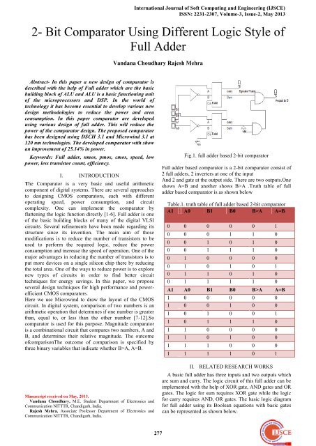
Fig.1. full adder based 2-bit comparator<br />
<strong>Full</strong> adder based comparator is a 2-bit comparator consist <strong>of</strong><br />
2 full adders, 2 inverters at one <strong>of</strong> the input<br />
And 2 and gate at the output side. There are two outputs.One<br />
shows A=B and another shows B>A .Truth table <strong>of</strong> full<br />
adder based comparator is as shown below<br />
Table.1. truth table <strong>of</strong> full adder based 2-bit comparator<br />
A1 A0 B1 B0 B>A A=B<br />
0 0 0 0 0 1<br />
0 0 0 1 1 0<br />
0 0 1 0 1 0<br />
0 0 1 1 1 0<br />
0 1 0 0 0 0<br />
0 1 0 1 0 1<br />
0 1 1 0 1 0<br />
0 1 1 1 1 0<br />
A1 A0 B1 B0 B>A A=B<br />
1 0 0 0 0 0<br />
1 0 0 1 0 0<br />
1 0 1 0 0 1<br />
1 0 1 1 1 0<br />
1 1 0 0 0 0<br />
1 1 0 1 0 0<br />
1 1 1 0 0 0<br />
1 1 1 1 0 1<br />
Manuscript received on May, 2013.<br />
Vandana Choudhary, M.E. Student Department <strong>of</strong> Electronics and<br />
Communication NITTTR, Chandigarh, India.<br />
Rajesh Mehra, Associate Pr<strong>of</strong>essor Department <strong>of</strong> Electronics and<br />
Communication NITTTR, Chandigarh, India.<br />
II. RELATED RESEARCH WORKS<br />
A basic full adder has three inputs and two outputs which<br />
are sum and carry. The logic circuit <strong>of</strong> this full adder can be<br />
implemented with the help <strong>of</strong> XOR gate, AND gates and OR<br />
gates. The logic for sum requires XOR gate while the logic<br />
for carry requires AND, OR gates. The basic logic diagram<br />
for full adder using its Boolean equations with basic gates<br />
can be represented as shown below.<br />
277
2- <strong>Bit</strong> <strong>Comparator</strong> <strong>Using</strong> <strong>Different</strong> <strong>Logic</strong> <strong>Style</strong> <strong>of</strong> <strong>Full</strong> <strong>Adder</strong><br />
The logic diagram <strong>of</strong> hybrid comparator is as shown<br />
below .this logic style consist <strong>of</strong> two xor gate and one<br />
multiplexer.<br />
Fig.2.<strong>Logic</strong> diagram <strong>of</strong> basic full adder<br />
The XOR gate is the basic building block <strong>of</strong> the full adder<br />
circuit. The performance <strong>of</strong> the full adder can be improved<br />
by enhancing the performance <strong>of</strong> the XOR gate. Several<br />
refinements have been made in its structure in terms <strong>of</strong><br />
transistors to increase the performance <strong>of</strong> full adder. The<br />
early designs <strong>of</strong> XOR gates were based on eight transistors<br />
or six transistors that are conventionally used in most<br />
designs. The main intention <strong>of</strong> reducing this transistor count<br />
is to reduce the size <strong>of</strong> XOR gate so that large number <strong>of</strong><br />
devices can be configured on a single silicon chip. There by<br />
reducing the area and delay. There by educing the area and<br />
delay. reducing the area and delay.<br />
Fig.5.logic diagram <strong>of</strong> hybrid comparator<br />
The comparator using hybrid full adder is shown in<br />
fig.6.the comparator consumes more power and area as<br />
compared to the basic full adder based comparator. It<br />
consists <strong>of</strong> four xor gate, two multiplexer, two not gate and<br />
two AND gate. <strong>Comparator</strong> has four input (A1, A0, B1, B0)<br />
and two output (A=B, B>A).<br />
Fig.6.logic diagram <strong>of</strong> hybrid full adder based comparator<br />
The layout design <strong>of</strong> hybrid full adder based <strong>Comparator</strong> is<br />
shown in fig.7.<br />
Fig.3.<strong>Logic</strong> diagram <strong>of</strong> basic full adder comparator<br />
The layout design <strong>of</strong> the basic full adder based<br />
comparator is shown in fig.4... layout is the general concept<br />
that describes the geometrical representation <strong>of</strong> the circuits<br />
by the means <strong>of</strong> layers.<strong>Different</strong> logical layers is used by<br />
designers to generate the layout.<br />
Fig.7.layout design <strong>of</strong> hybrid full adder based comparator<br />
Fig.4.layout design <strong>of</strong> basic full adder based comparator<br />
III. PROPOSED WORK<br />
Proposed work <strong>of</strong> comparator is based on another logic<br />
style <strong>of</strong> full adder.thislogic style <strong>of</strong> comparator provides less<br />
power consumption than other logic styles described in this<br />
paper. The implementation <strong>of</strong> new logic full adder based<br />
comparator is shown in fig.9.It consists <strong>of</strong> two full adders,<br />
two not gates at one <strong>of</strong> the input and two AND gates at the<br />
output <strong>of</strong> the comparator. It has four input (A1, B1, A0, B0)<br />
and two output (A=B, B>A).<br />
278
International Journal <strong>of</strong> S<strong>of</strong>t Computing and Engineering (IJSCE)<br />
ISSN: 2231-2307, Volume-3, Issue-2, May 2013<br />
in table.2. Simulations are obtained in Microwind Tool. First<br />
step in obtaining the simulations is to compile the Verilog<br />
file in Microwind 3.1. Verilog file is created from the circuit<br />
diagram, which is designed in the schematic. The Verilog<br />
file is now compiled in Microwind 3.1. After the<br />
compilation <strong>of</strong> Verilog file, the layout for the circuit<br />
diagram drawn in schematic will be generated in<br />
Microwind. After that simulations are performed on the<br />
layout generated using Verilog files. The results are<br />
simulated at room temperature.<br />
Table.2.Simulation results <strong>of</strong> various full adder based<br />
comparator<br />
Fig.8.logic diagram <strong>of</strong> full adder using logic<br />
Basic<br />
comparator<br />
Hybrid<br />
comparator<br />
Proposed<br />
comparator<br />
Routed 25 36 30<br />
wires<br />
Width 33.7 64.4 77.9<br />
Height 9.8 9.4 10.3<br />
Area 331.8 603.2 803.7<br />
Power 27.725 42.480 26.286<br />
V. CONCLUSION<br />
This paper describes different logic styles <strong>of</strong> full adder for<br />
designing a comparator for low Power Consumption. Basic<br />
full adder based comparator <strong>Logic</strong> <strong>Style</strong> provides low power<br />
and area design as compared to other <strong>Logic</strong> <strong>Style</strong>. Hybrid<br />
comparator logic style provides high power consumption &<br />
area. The proposed comparator consumes less power as<br />
compared to other logic styles. But the area consumption is<br />
greater than basic full adder based comparator. By using the<br />
proposed architecture the power is reduced up to 0.439 mw<br />
and area is increased up to 602.6 μm² than the other logic<br />
styles. Future scope for this paper is area reduction.<br />
Fig.9.logic diagram <strong>of</strong> proposed full adder based comparator<br />
The layout design <strong>of</strong> comparator using another logic <strong>of</strong> full<br />
adder is shown in fig.10.layout is the general concept that<br />
describes the geometrical representation <strong>of</strong> the circuits by<br />
the means <strong>of</strong> layers and polygons. <strong>Different</strong> logical layers<br />
are used by designers to generate the layout. <strong>Different</strong><br />
logical layers are used by the designers to generate the<br />
layout.<br />
Fig.10.layout design <strong>of</strong> proposed full adder based<br />
comparator<br />
IV. ANALYSIS AND COMPARISON<br />
Analysis and comparison <strong>of</strong> different logic styles <strong>of</strong><br />
comparator using various logic styles <strong>of</strong> full adder is shown<br />
REFERENCES<br />
[1] H. Traff, “Noval approach to high speed CMOS current<br />
<strong>Comparator</strong>,” Electron. Letter, vol. 28, no. 3, pp. 310- 312,<br />
Jan.1992.<br />
[2] A.T K. Tang and C. Toumazou, “High performance CMOS current<br />
comparator,” Electron. Letter, vol. 30, pp. 5-6, 1994.<br />
[3] L. Ravezzi, D. Stoppa and G. F. Dalla Betta, “Simple High speed<br />
CMOS current comparator,” Electron. Letter, vol.33, pp.1829-1830,<br />
1997.<br />
[4] C. B. Kushwah, D. Soni and R. S. Gamad, “New design <strong>of</strong> CMOS<br />
Current comparator,” Second International Conference on Emerging<br />
Trends in Engineering and Technology, ICETET, pp.125-129, June,<br />
2009.<br />
[5]. Current <strong>Comparator</strong> Design,” Electron. Letter, vol. 44, no.3,pp.171-<br />
172, Jan. 2008.<br />
[6] Lu Chen, Bingxue Shi and Chun Lu, “A Robust High-Speed and<br />
Low-power CMOS Current <strong>Comparator</strong> Circuit,” IEEE Asia-Pacific<br />
Conf. On Circuits and Systems, pp. 174-177, 2000.<br />
[7] S. Rahul, F. L. Richard and M. Carver, “A Low Power Wide<br />
Dynamic-Range Analog VLSI Cochlea,” Analog Integral Circuits<br />
Signal Process, vol. 16, pp. 245– 274, 1998.<br />
[8] P. F. Ruedi, P. Heim, F. Kaese, E. Grenet, F. Heitger, P. Y. Burgi,S.<br />
Gyger and P. Nussbaum, “A 128X128 pixel 120 dB dynamic range<br />
vision-sensor chip for image contrast and orientation extraction, ”<br />
IEEE Journal Solid-State Circuits, vol. 38,pp. 2325-2333, 2003.<br />
[9] Niels van Bakel, Jo van den Brand, “Design <strong>of</strong> a comparator in a<br />
0.25μm CMOS technology”.<br />
[10] Sung-Mo Kang and Yusuf Leblebici, “CMOS Digital Integrated<br />
Circuits Analysis and Design”, Tata McGraw-Hill third edition.<br />
[11 Jan M. Rabaey, Anantha Chandrakasan and Borivoje Nikolic,<br />
“Digital Integrated Circuit”, Pearson Education Electronics and<br />
VLSI series, second edition.]<br />
279