Atmel ATMEGA128A-AU datasheet - Octopart
Atmel ATMEGA128A-AU datasheet - Octopart
Atmel ATMEGA128A-AU datasheet - Octopart

You also want an ePaper? Increase the reach of your titles
YUMPU automatically turns print PDFs into web optimized ePapers that Google loves.
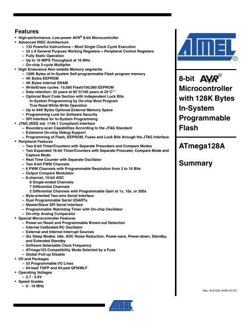
Features<br />
• High-performance, Low-power AVR ® 8-bit Microcontroller<br />
• Advanced RISC Architecture<br />
– 133 Powerful Instructions – Most Single Clock Cycle Execution<br />
– 32 x 8 General Purpose Working Registers + Peripheral Control Registers<br />
– Fully Static Operation<br />
– Up to 16 MIPS Throughput at 16 MHz<br />
– On-chip 2-cycle Multiplier<br />
• High Endurance Non-volatile Memory segments<br />
– 128K Bytes of In-System Self-programmable Flash program memory<br />
– 4K Bytes EEPROM<br />
– 4K Bytes Internal SRAM<br />
– Write/Erase cycles: 10,000 Flash/100,000 EEPROM<br />
– Data retention: 20 years at 85°C/100 years at 25°C (1)<br />
– Optional Boot Code Section with Independent Lock Bits<br />
In-System Programming by On-chip Boot Program<br />
True Read-While-Write Operation<br />
– Up to 64K Bytes Optional External Memory Space<br />
– Programming Lock for Software Security<br />
– SPI Interface for In-System Programming<br />
• JTAG (IEEE std. 1149.1 Compliant) Interface<br />
– Boundary-scan Capabilities According to the JTAG Standard<br />
– Extensive On-chip Debug Support<br />
– Programming of Flash, EEPROM, Fuses and Lock Bits through the JTAG Interface<br />
• Peripheral Features<br />
– Two 8-bit Timer/Counters with Separate Prescalers and Compare Modes<br />
– Two Expanded 16-bit Timer/Counters with Separate Prescaler, Compare Mode and<br />
Capture Mode<br />
– Real Time Counter with Separate Oscillator<br />
– Two 8-bit PWM Channels<br />
– 6 PWM Channels with Programmable Resolution from 2 to 16 Bits<br />
– Output Compare Modulator<br />
– 8-channel, 10-bit ADC<br />
8 Single-ended Channels<br />
7 Differential Channels<br />
2 Differential Channels with Programmable Gain at 1x, 10x, or 200x<br />
– Byte-oriented Two-wire Serial Interface<br />
– Dual Programmable Serial USARTs<br />
– Master/Slave SPI Serial Interface<br />
– Programmable Watchdog Timer with On-chip Oscillator<br />
– On-chip Analog Comparator<br />
• Special Microcontroller Features<br />
– Power-on Reset and Programmable Brown-out Detection<br />
– Internal Calibrated RC Oscillator<br />
– External and Internal Interrupt Sources<br />
– Six Sleep Modes: Idle, ADC Noise Reduction, Power-save, Power-down, Standby,<br />
and Extended Standby<br />
– Software Selectable Clock Frequency<br />
– ATmega103 Compatibility Mode Selected by a Fuse<br />
– Global Pull-up Disable<br />
• I/O and Packages<br />
– 53 Programmable I/O Lines<br />
– 64-lead TQFP and 64-pad QFN/MLF<br />
• Operating Voltages<br />
– 2.7 - 5.5V<br />
• Speed Grades<br />
– 0 - 16 MHz<br />
8-bit<br />
Microcontroller<br />
with 128K Bytes<br />
In-System<br />
Programmable<br />
Flash<br />
ATmega128A<br />
Summary<br />
Rev. 8151GS–AVR–07/10
ATmega128A<br />
1. Pin Configurations<br />
Figure 1-1.<br />
Pinout ATmega128A<br />
PEN<br />
RXD0/(PDI) PE0<br />
(TXD0/PDO) PE1<br />
(XCK0/AIN0) PE2<br />
(OC3A/AIN1) PE3<br />
(OC3B/INT4) PE4<br />
(OC3C/INT5) PE5<br />
(T3/INT6) PE6<br />
(ICP3/INT7) PE7<br />
(SS) PB0<br />
(SCK) PB1<br />
(MOSI) PB2<br />
(MISO) PB3<br />
(OC0) PB4<br />
(OC1A) PB5<br />
(OC1B) PB6<br />
1<br />
2<br />
3<br />
4<br />
5<br />
6<br />
7<br />
8<br />
9<br />
10<br />
11<br />
12<br />
13<br />
14<br />
15<br />
16<br />
64<br />
63<br />
62<br />
61<br />
60<br />
59<br />
58<br />
57<br />
56<br />
55<br />
54<br />
53<br />
52<br />
51<br />
50<br />
49<br />
17<br />
18<br />
19<br />
20<br />
21<br />
22<br />
23<br />
24<br />
25<br />
26<br />
27<br />
28<br />
29<br />
30<br />
31<br />
32<br />
48<br />
47<br />
46<br />
45<br />
44<br />
43<br />
42<br />
41<br />
40<br />
39<br />
38<br />
37<br />
36<br />
35<br />
34<br />
33<br />
PA3 (AD3)<br />
PA4 (AD4)<br />
PA5 (AD5)<br />
PA6 (AD6)<br />
PA7 (AD7)<br />
PG2(ALE)<br />
PC7 (A15)<br />
PC6 (A14)<br />
PC5 (A13)<br />
PC4 (A12)<br />
PC3 (A11)<br />
PC2 (A10)<br />
PC1 (A9)<br />
PC0 (A8)<br />
PG1(RD)<br />
PG0(WR)<br />
(OC2/OC1C) PB7<br />
TOSC2/PG3<br />
TOSC1/PG4<br />
RESET<br />
VCC<br />
GND<br />
XTAL2<br />
XTAL1<br />
(SCL/INT0) PD0<br />
(SDA/INT1) PD1<br />
(RXD1/INT2) PD2<br />
(TXD1/INT3) PD3<br />
(ICP1) PD4<br />
(XCK1) PD5<br />
(T1) PD6<br />
(T2) PD7<br />
AVCC<br />
GND<br />
AREF<br />
PF0 (ADC0)<br />
PF1 (ADC1)<br />
PF2 (ADC2)<br />
PF3 (ADC3)<br />
PF4 (ADC4/TCK)<br />
PF5 (ADC5/TMS)<br />
PF6 (ADC6/TDO)<br />
PF7 (ADC7/TDI)<br />
GND<br />
VCC<br />
PA0 (AD0)<br />
PA1 (AD1)<br />
PA2 (AD2)<br />
Note:<br />
The Pinout figure applies to both TQFP and MLF packages. The bottom pad under the QFN/MLF<br />
package should be soldered to ground.<br />
2. Overview<br />
The ATmega128A is a low-power CMOS 8-bit microcontroller based on the AVR enhanced<br />
RISC architecture. By executing powerful instructions in a single clock cycle, the ATmega128A<br />
achieves throughputs approaching 1 MIPS per MHz allowing the system designer to optimize<br />
power consumption versus processing speed.<br />
19<br />
8151GS–AVR–07/10
-<br />
ATmega128A<br />
2.1 Block Diagram<br />
Figure 2-1.<br />
Block Diagram<br />
PF0 - PF7<br />
PA0 - PA7<br />
PC0 - PC7<br />
XTAL1<br />
XTAL2<br />
RESET<br />
VCC<br />
GND<br />
PORTF DRIVERS<br />
PORTA DRIVERS<br />
PORTC DRIVERS<br />
DATA REGISTER<br />
PORTF<br />
DATA DIR.<br />
REG. PORTF<br />
DATA REGISTER<br />
PORTA<br />
DATA DIR.<br />
REG. PORTA<br />
DATA REGISTER<br />
PORTC<br />
DATA DIR.<br />
REG. PORTC<br />
8-BIT DATA BUS<br />
AVCC<br />
AGND<br />
AREF<br />
ADC<br />
INTERNAL<br />
OSCILLATOR<br />
CALIB. OSC<br />
OSCILLATOR<br />
JTAG TAP<br />
PROGRAM<br />
COUNTER<br />
STACK<br />
POINTER<br />
WATCHDOG<br />
TIMER<br />
OSCILLATOR<br />
ON-CHIP DEBUG<br />
PROGRAM<br />
FLASH<br />
SRAM<br />
MCU CONTROL<br />
REGISTER<br />
TIMING AND<br />
CONTROL<br />
BOUNDARY-<br />
SCAN<br />
INSTRUCTION<br />
REGISTER<br />
GENERAL<br />
PURPOSE<br />
REGISTERS<br />
TIMER/<br />
COUNTERS<br />
PEN<br />
PROGRAMMING<br />
LOGIC<br />
INSTRUCTION<br />
DECODER<br />
X<br />
Y<br />
Z<br />
INTERRUPT<br />
UNIT<br />
CONTROL<br />
LINES<br />
ALU<br />
EEPROM<br />
STATUS<br />
REGISTER<br />
USART0<br />
SPI<br />
USART1<br />
TWO-WIRE SERIAL<br />
INTERFACE<br />
ANALOG<br />
COMPARATOR<br />
+<br />
DATA REGISTER<br />
PORTE<br />
DATA DIR.<br />
REG. PORTE<br />
DATA REGISTER<br />
PORTB<br />
DATA DIR.<br />
REG. PORTB<br />
DATA REGISTER<br />
PORTD<br />
DATA DIR.<br />
REG. PORTD<br />
DATA REG.<br />
PORTG<br />
DATA DIR.<br />
REG. PORTG<br />
PORTE DRIVERS<br />
PORTB DRIVERS<br />
PORTD DRIVERS<br />
PORTG DRIVERS<br />
PE0 - PE7<br />
PB0 - PB7<br />
PD0 - PD7<br />
PG0 - PG4<br />
8151GS–AVR–07/10<br />
19
ATmega128A<br />
The AVR core combines a rich instruction set with 32 general purpose working registers. All the<br />
32 registers are directly connected to the Arithmetic Logic Unit (ALU), allowing two independent<br />
registers to be accessed in one single instruction executed in one clock cycle. The resulting<br />
architecture is more code efficient while achieving throughputs up to ten times faster than conventional<br />
CISC microcontrollers.<br />
The ATmega128A provides the following features: 128K bytes of In-System Programmable<br />
Flash with Read-While-Write capabilities, 4K bytes EEPROM, 4K bytes SRAM, 53 general purpose<br />
I/O lines, 32 general purpose working registers, Real Time Counter (RTC), four flexible<br />
Timer/Counters with compare modes and PWM, 2 USARTs, a byte oriented Two-wire Serial<br />
Interface, an 8-channel, 10-bit ADC with optional differential input stage with programmable<br />
gain, programmable Watchdog Timer with Internal Oscillator, an SPI serial port, IEEE std.<br />
1149.1 compliant JTAG test interface, also used for accessing the On-chip Debug system and<br />
programming and six software selectable power saving modes. The Idle mode stops the CPU<br />
while allowing the SRAM, Timer/Counters, SPI port, and interrupt system to continue functioning.<br />
The Power-down mode saves the register contents but freezes the Oscillator, disabling all<br />
other chip functions until the next interrupt or Hardware Reset. In Power-save mode, the asynchronous<br />
timer continues to run, allowing the user to maintain a timer base while the rest of the<br />
device is sleeping. The ADC Noise Reduction mode stops the CPU and all I/O modules except<br />
Asynchronous Timer and ADC, to minimize switching noise during ADC conversions. In Standby<br />
mode, the Crystal/Resonator Oscillator is running while the rest of the device is sleeping. This<br />
allows very fast start-up combined with low power consumption. In Extended Standby mode,<br />
both the main Oscillator and the Asynchronous Timer continue to run.<br />
The device is manufactured using <strong>Atmel</strong>’s high-density nonvolatile memory technology. The Onchip<br />
ISP Flash allows the program memory to be reprogrammed in-system through an SPI serial<br />
interface, by a conventional nonvolatile memory programmer, or by an On-chip Boot program<br />
running on the AVR core. The boot program can use any interface to download the application<br />
program in the application Flash memory. Software in the Boot Flash section will continue to run<br />
while the Application Flash section is updated, providing true Read-While-Write operation. By<br />
combining an 8-bit RISC CPU with In-System Self-Programmable Flash on a monolithic chip,<br />
the <strong>Atmel</strong> ATmega128A is a powerful microcontroller that provides a highly flexible and cost<br />
effective solution to many embedded control applications.<br />
The ATmega128A AVR is supported with a full suite of program and system development tools<br />
including: C compilers, macro assemblers, program debugger/simulators, in-circuit emulators,<br />
and evaluation kits.<br />
2.2 ATmega103 and ATmega128A Compatibility<br />
The ATmega128A is a highly complex microcontroller where the number of I/O locations supersedes<br />
the 64 I/O locations reserved in the AVR instruction set. To ensure backward compatibility<br />
with the ATmega103, all I/O locations present in ATmega103 have the same location in<br />
ATmega128A. Most additional I/O locations are added in an Extended I/O space starting from<br />
$60 to $FF, (i.e., in the ATmega103 internal RAM space). These locations can be reached by<br />
using LD/LDS/LDD and ST/STS/STD instructions only, not by using IN and OUT instructions.<br />
The relocation of the internal RAM space may still be a problem for ATmega103 users. Also, the<br />
increased number of interrupt vectors might be a problem if the code uses absolute addresses.<br />
To solve these problems, an ATmega103 compatibility mode can be selected by programming<br />
the fuse M103C. In this mode, none of the functions in the Extended I/O space are in use, so the<br />
internal RAM is located as in ATmega103. Also, the Extended Interrupt vectors are removed.<br />
8151GS–AVR–07/10<br />
19
ATmega128A<br />
The ATmega128A is 100% pin compatible with ATmega103, and can replace the ATmega103<br />
on current Printed Circuit Boards. The application note “Replacing ATmega103 by<br />
ATmega128A” describes what the user should be aware of replacing the ATmega103 by an<br />
ATmega128A.<br />
2.2.1 ATmega103 Compatibility Mode<br />
By programming the M103C fuse, the ATmega128 will be compatible with the ATmega103<br />
regards to RAM, I/O pins and interrupt vectors as described above. However, some new features<br />
in ATmega128 are not available in this compatibility mode, these features are listed below:<br />
2.3 Pin Descriptions<br />
• One USART instead of two, Asynchronous mode only. Only the eight least significant bits of<br />
the Baud Rate Register is available.<br />
• One 16 bits Timer/Counter with two compare registers instead of two 16-bit Timer/Counters<br />
with three compare registers.<br />
• Two-wire serial interface is not supported.<br />
• Port C is output only.<br />
• Port G serves alternate functions only (not a general I/O port).<br />
• Port F serves as digital input only in addition to analog input to the ADC.<br />
• Boot Loader capabilities is not supported.<br />
• It is not possible to adjust the frequency of the internal calibrated RC Oscillator.<br />
• The External Memory Interface can not release any Address pins for general I/O, neither<br />
configure different wait-states to different External Memory Address sections.<br />
• In addition, there are some other minor differences to make it more compatible to<br />
ATmega103:<br />
• Only EXTRF and PORF exists in MCUCSR.<br />
• Timed sequence not required for Watchdog Time-out change.<br />
• External Interrupt pins 3 - 0 serve as level interrupt only.<br />
• USART has no FIFO buffer, so data overrun comes earlier.<br />
Unused I/O bits in ATmega103 should be written to 0 to ensure same operation in ATmega128.<br />
2.3.1 VCC<br />
2.3.2 GND<br />
Digital supply voltage.<br />
Ground.<br />
2.3.3 Port A (PA7:PA0)<br />
Port A is an 8-bit bi-directional I/O port with internal pull-up resistors (selected for each bit). The<br />
Port A output buffers have symmetrical drive characteristics with both high sink and source<br />
capability. As inputs, Port A pins that are externally pulled low will source current if the pull-up<br />
resistors are activated. The Port A pins are tri-stated when a reset condition becomes active,<br />
even if the clock is not running.<br />
Port A also serves the functions of various special features of the ATmega128A as listed on<br />
page 73.<br />
8151GS–AVR–07/10<br />
19
ATmega128A<br />
2.3.4 Port B (PB7:PB0)<br />
Port B is an 8-bit bi-directional I/O port with internal pull-up resistors (selected for each bit). The<br />
Port B output buffers have symmetrical drive characteristics with both high sink and source<br />
capability. As inputs, Port B pins that are externally pulled low will source current if the pull-up<br />
resistors are activated. The Port B pins are tri-stated when a reset condition becomes active,<br />
even if the clock is not running.<br />
Port B also serves the functions of various special features of the ATmega128A as listed on<br />
page 74.<br />
2.3.5 Port C (PC7:PC0)<br />
Port C is an 8-bit bi-directional I/O port with internal pull-up resistors (selected for each bit). The<br />
Port C output buffers have symmetrical drive characteristics with both high sink and source<br />
capability. As inputs, Port C pins that are externally pulled low will source current if the pull-up<br />
resistors are activated. The Port C pins are tri-stated when a reset condition becomes active,<br />
even if the clock is not running.<br />
Port C also serves the functions of special features of the ATmega128A as listed on page 76. In<br />
ATmega103 compatibility mode, Port C is output only, and the port C pins are not tri-stated<br />
when a reset condition becomes active.<br />
Note:<br />
The ATmega128A is by default shipped in ATmega103 compatibility mode. Thus, if the parts are<br />
not programmed before they are put on the PCB, PORTC will be output during first power up, and<br />
until the ATmega103 compatibility mode is disabled.<br />
2.3.6 Port D (PD7:PD0)<br />
Port D is an 8-bit bi-directional I/O port with internal pull-up resistors (selected for each bit). The<br />
Port D output buffers have symmetrical drive characteristics with both high sink and source<br />
capability. As inputs, Port D pins that are externally pulled low will source current if the pull-up<br />
resistors are activated. The Port D pins are tri-stated when a reset condition becomes active,<br />
even if the clock is not running.<br />
Port D also serves the functions of various special features of the ATmega128A as listed on<br />
page 78.<br />
2.3.7 Port E (PE7:PE0)<br />
Port E is an 8-bit bi-directional I/O port with internal pull-up resistors (selected for each bit). The<br />
Port E output buffers have symmetrical drive characteristics with both high sink and source<br />
capability. As inputs, Port E pins that are externally pulled low will source current if the pull-up<br />
resistors are activated. The Port E pins are tri-stated when a reset condition becomes active,<br />
even if the clock is not running.<br />
Port E also serves the functions of various special features of the ATmega128A as listed on<br />
page 81.<br />
2.3.8 Port F (PF7:PF0)<br />
Port F serves as the analog inputs to the A/D Converter.<br />
Port F also serves as an 8-bit bi-directional I/O port, if the A/D Converter is not used. Port pins<br />
can provide internal pull-up resistors (selected for each bit). The Port F output buffers have symmetrical<br />
drive characteristics with both high sink and source capability. As inputs, Port F pins<br />
that are externally pulled low will source current if the pull-up resistors are activated. The Port F<br />
pins are tri-stated when a reset condition becomes active, even if the clock is not running. If the<br />
8151GS–AVR–07/10<br />
19
ATmega128A<br />
JTAG interface is enabled, the pull-up resistors on pins PF7(TDI), PF5(TMS), and PF4(TCK) will<br />
be activated even if a Reset occurs.<br />
The TDO pin is tri-stated unless TAP states that shift out data are entered.<br />
Port F also serves the functions of the JTAG interface.<br />
In ATmega103 compatibility mode, Port F is an input Port only.<br />
2.3.9 Port G (PG4:PG0)<br />
Port G is a 5-bit bi-directional I/O port with internal pull-up resistors (selected for each bit). The<br />
Port G output buffers have symmetrical drive characteristics with both high sink and source<br />
capability. As inputs, Port G pins that are externally pulled low will source current if the pull-up<br />
resistors are activated. The Port G pins are tri-stated when a reset condition becomes active,<br />
even if the clock is not running.<br />
Port G also serves the functions of various special features.<br />
The port G pins are tri-stated when a reset condition becomes active, even if the clock is not<br />
running.<br />
In ATmega103 compatibility mode, these pins only serves as strobes signals to the external<br />
memory as well as input to the 32 kHz Oscillator, and the pins are initialized to PG0 = 1,<br />
PG1 = 1, and PG2 = 0 asynchronously when a reset condition becomes active, even if the clock<br />
is not running. PG3 and PG4 are oscillator pins.<br />
2.3.10 RESET<br />
2.3.11 XTAL1<br />
2.3.12 XTAL2<br />
2.3.13 AVCC<br />
2.3.14 AREF<br />
2.3.15 PEN<br />
Reset input. A low level on this pin for longer than the minimum pulse length will generate a<br />
reset, even if the clock is not running. The minimum pulse length is given in “System and Reset<br />
Characteristics” on page 324. Shorter pulses are not guaranteed to generate a reset.<br />
Input to the inverting Oscillator amplifier and input to the internal clock operating circuit.<br />
Output from the inverting Oscillator amplifier.<br />
AVCC is the supply voltage pin for Port F and the A/D Converter. It should be externally connected<br />
to V CC , even if the ADC is not used. If the ADC is used, it should be connected to V CC<br />
through a low-pass filter.<br />
AREF is the analog reference pin for the A/D Converter.<br />
PEN is a programming enable pin for the SPI Serial Programming mode, and is internally pulled<br />
high . By holding this pin low during a Power-on Reset, the device will enter the SPI Serial Programming<br />
mode. PEN has no function during normal operation.<br />
8151GS–AVR–07/10<br />
19
ATmega128A<br />
3. Resources<br />
A comprehensive set of development tools, application notes, and <strong>datasheet</strong>s are available for<br />
download on http://www.atmel.com/avr.<br />
ATmega128A/L rev. A - M characterization is found in the ATmega128A Appendix B.<br />
Note: 1.<br />
4. Data Retention<br />
Reliability Qualification results show that the projected data retention failure rate is much less<br />
than 1 PPM over 20 years at 85°C or 100 years at 25°C.<br />
8151GS–AVR–07/10<br />
19
ATmega128A<br />
5. Register Summary (Continued)<br />
Address Name Bit 7 Bit 6 Bit 5 Bit 4 Bit 3 Bit 2 Bit 1 Bit 0 Page<br />
($FF) Reserved – – – – – – – –<br />
: Reserved – – – – – – – –<br />
($9E) Reserved – – – – – – – –<br />
($9D) UCSR1C – UMSEL1 UPM11 UPM10 USBS1 UCSZ11 UCSZ10 UCPOL1 195<br />
($9C) UDR1 USART1 I/O Data Register 192<br />
($9B) UCSR1A RXC1 TXC1 UDRE1 FE1 DOR1 UPE1 U2X1 MPCM1 193<br />
($9A) UCSR1B RXCIE1 TXCIE1 UDRIE1 RXEN1 TXEN1 UCSZ12 RXB81 TXB81 194<br />
($99) UBRR1L USART1 Baud Rate Register Low 197<br />
($98) UBRR1H – – – – USART1 Baud Rate Register High 197<br />
($97) Reserved – – – – – – – –<br />
($96) Reserved – – – – – – – –<br />
($95) UCSR0C – UMSEL0 UPM01 UPM00 USBS0 UCSZ01 UCSZ00 UCPOL0 195<br />
($94) Reserved – – – – – – – –<br />
($93) Reserved – – – – – – – –<br />
($92) Reserved – – – – – – – –<br />
($91) Reserved – – – – – – – –<br />
($90) UBRR0H – – – – USART0 Baud Rate Register High 197<br />
($8F) Reserved – – – – – – – –<br />
($8E) Reserved – – – – – – – –<br />
($8D) Reserved – – – – – – – –<br />
($8C) TCCR3C FOC3A FOC3B FOC3C – – – – – 138<br />
($8B) TCCR3A COM3A1 COM3A0 COM3B1 COM3B0 COM3C1 COM3C0 WGM31 WGM30 134<br />
($8A) TCCR3B ICNC3 ICES3 – WGM33 WGM32 CS32 CS31 CS30 137<br />
($89) TCNT3H Timer/Counter3 – Counter Register High Byte 139<br />
($88) TCNT3L Timer/Counter3 – Counter Register Low Byte 139<br />
($87) OCR3AH Timer/Counter3 – Output Compare Register A High Byte 140<br />
($86) OCR3AL Timer/Counter3 – Output Compare Register A Low Byte 140<br />
($85) OCR3BH Timer/Counter3 – Output Compare Register B High Byte 140<br />
($84) OCR3BL Timer/Counter3 – Output Compare Register B Low Byte 140<br />
($83) OCR3CH Timer/Counter3 – Output Compare Register C High Byte 140<br />
($82) OCR3CL Timer/Counter3 – Output Compare Register C Low Byte 140<br />
($81) ICR3H Timer/Counter3 – Input Capture Register High Byte 141<br />
($80) ICR3L Timer/Counter3 – Input Capture Register Low Byte 141<br />
($7F) Reserved – – – – – – – –<br />
($7E) Reserved – – – – – – – –<br />
($7D) ETIMSK – – TICIE3 OCIE3A OCIE3B TOIE3 OCIE3C OCIE1C 142<br />
($7C) ETIFR – – ICF3 OCF3A OCF3B TOV3 OCF3C OCF1C 143<br />
($7B) Reserved – – – – – – – –<br />
($7A) TCCR1C FOC1A FOC1B FOC1C – – – – – 138<br />
($79) OCR1CH Timer/Counter1 – Output Compare Register C High Byte 140<br />
($78) OCR1CL Timer/Counter1 – Output Compare Register C Low Byte 140<br />
($77) Reserved – – – – – – – –<br />
($76) Reserved – – – – – – – –<br />
($75) Reserved – – – – – – – –<br />
($74) TWCR TWINT TWEA TWSTA TWSTO TWWC TWEN – TWIE 226<br />
($73) TWDR Two-wire Serial Interface Data Register 228<br />
($72) TWAR TWA6 TWA5 TWA4 TWA3 TWA2 TWA1 TWA0 TWGCE 229<br />
($71) TWSR TWS7 TWS6 TWS5 TWS4 TWS3 – TWPS1 TWPS0 228<br />
($70) TWBR Two-wire Serial Interface Bit Rate Register 226<br />
($6F) OSCCAL Oscillator Calibration Register 44<br />
($6E) Reserved – – – – – – – –<br />
($6D) XMCRA – SRL2 SRL1 SRL0 SRW01 SRW00 SRW11 34<br />
($6C) XMCRB XMBK – – – – XMM2 XMM1 XMM0 35<br />
($6B) Reserved – – – – – – – –<br />
($6A) EICRA ISC31 ISC30 ISC21 ISC20 ISC11 ISC10 ISC01 ISC00 90<br />
($69) Reserved – – – – – – – –<br />
($68) SPMCSR SPMIE RWWSB – RWWSRE BLBSET PGWRT PGERS SPMEN 289<br />
($67) Reserved – – – – – – – –<br />
($66) Reserved – – – – – – – –<br />
($65) PORTG – – – PORTG4 PORTG3 PORTG2 PORTG1 PORTG0 89<br />
($64) DDRG – – – DDG4 DDG3 DDG2 DDG1 DDG0 89<br />
($63) PING – – – PING4 PING3 PING2 PING1 PING0 89<br />
8151GS–AVR–07/10<br />
19
ATmega128A<br />
5. Register Summary (Continued)<br />
Address Name Bit 7 Bit 6 Bit 5 Bit 4 Bit 3 Bit 2 Bit 1 Bit 0 Page<br />
($62) PORTF PORTF7 PORTF6 PORTF5 PORTF4 PORTF3 PORTF2 PORTF1 PORTF0 89<br />
($61) DDRF DDF7 DDF6 DDF5 DDF4 DDF3 DDF2 DDF1 DDF0 89<br />
($60) Reserved – – – – – – – –<br />
$3F ($5F) SREG I T H S V N Z C 10<br />
$3E ($5E) SPH SP15 SP14 SP13 SP12 SP11 SP10 SP9 SP8 13<br />
$3D ($5D) SPL SP7 SP6 SP5 SP4 SP3 SP2 SP1 SP0 13<br />
$3C ($5C) XDIV XDIVEN XDIV6 XDIV5 XDIV4 XDIV3 XDIV2 XDIV1 XDIV0 38<br />
$3B ($5B) RAMPZ – – – – – – – RAMPZ0 14<br />
$3A ($5A) EICRB ISC71 ISC70 ISC61 ISC60 ISC51 ISC50 ISC41 ISC40 91<br />
$39 ($59) EIMSK INT7 INT6 INT5 INT4 INT3 INT2 INT1 INT0 92<br />
$38 ($58) EIFR INTF7 INTF6 INTF5 INTF4 INTF3 INTF INTF1 INTF0 92<br />
$37 ($57) TIMSK OCIE2 TOIE2 TICIE1 OCIE1A OCIE1B TOIE1 OCIE0 TOIE0 110, 141, 162<br />
$36 ($56) TIFR OCF2 TOV2 ICF1 OCF1A OCF1B TOV1 OCF0 TOV0 110, 143, 162<br />
$35 ($55) MCUCR SRE SRW10 SE SM1 SM0 SM2 IVSEL IVCE 33, 50, 63<br />
$34 ($54) MCUCSR JTD – – JTRF WDRF BORF EXTRF PORF 56, 257<br />
$33 ($53) TCCR0 FOC0 WGM00 COM01 COM00 WGM01 CS02 CS01 CS00 106<br />
$32 ($52) TCNT0 Timer/Counter0 (8 Bit) 109<br />
$31 ($51) OCR0 Timer/Counter0 Output Compare Register 109<br />
$30 ($50) ASSR – – – – AS0 TCN0UB OCR0UB TCR0UB 109<br />
$2F ($4F) TCCR1A COM1A1 COM1A0 COM1B1 COM1B0 COM1C1 COM1C0 WGM11 WGM10 134<br />
$2E ($4E) TCCR1B ICNC1 ICES1 – WGM13 WGM12 CS12 CS11 CS10 137<br />
$2D ($4D) TCNT1H Timer/Counter1 – Counter Register High Byte 139<br />
$2C ($4C) TCNT1L Timer/Counter1 – Counter Register Low Byte 139<br />
$2B ($4B) OCR1AH Timer/Counter1 – Output Compare Register A High Byte 139<br />
$2A ($4A) OCR1AL Timer/Counter1 – Output Compare Register A Low Byte 139<br />
$29 ($49) OCR1BH Timer/Counter1 – Output Compare Register B High Byte 139<br />
$28 ($48) OCR1BL Timer/Counter1 – Output Compare Register B Low Byte 139<br />
$27 ($47) ICR1H Timer/Counter1 – Input Capture Register High Byte 140<br />
$26 ($46) ICR1L Timer/Counter1 – Input Capture Register Low Byte 140<br />
$25 ($45) TCCR2 FOC2 WGM20 COM21 COM20 WGM21 CS22 CS21 CS20 159<br />
$24 ($44) TCNT2 Timer/Counter2 (8 Bit) 161<br />
$23 ($43) OCR2 Timer/Counter2 Output Compare Register 162<br />
$22 ($42) OCDR IDRD/OCDR7 OCDR6 OCDR5 OCDR4 OCDR3 OCDR2 OCDR1 OCDR0 276<br />
$21 ($41) WDTCR – – – WDCE WDE WDP2 WDP1 WDP0 57<br />
$20 ($40) SFIOR TSM – – – ACME PUD PSR0 PSR321 86, 111, 146, 231<br />
$1F ($3F) EEARH – – – – EEPROM Address Register High 30<br />
$1E ($3E) EEARL EEPROM Address Register Low Byte 30<br />
$1D ($3D) EEDR EEPROM Data Register 30<br />
$1C ($3C) EECR – – – – EERIE EEMWE EEWE EERE 30<br />
$1B ($3B) PORTA PORTA7 PORTA6 PORTA5 PORTA4 PORTA3 PORTA2 PORTA1 PORTA0 87<br />
$1A ($3A) DDRA DDA7 DDA6 DDA5 DDA4 DDA3 DDA2 DDA1 DDA0 87<br />
$19 ($39) PINA PINA7 PINA6 PINA5 PINA4 PINA3 PINA2 PINA1 PINA0 87<br />
$18 ($38) PORTB PORTB7 PORTB6 PORTB5 PORTB4 PORTB3 PORTB2 PORTB1 PORTB0 87<br />
$17 ($37) DDRB DDB7 DDB6 DDB5 DDB4 DDB3 DDB2 DDB1 DDB0 87<br />
$16 ($36) PINB PINB7 PINB6 PINB5 PINB4 PINB3 PINB2 PINB1 PINB0 87<br />
$15 ($35) PORTC PORTC7 PORTC6 PORTC5 PORTC4 PORTC3 PORTC2 PORTC1 PORTC0 87<br />
$14 ($34) DDRC DDC7 DDC6 DDC5 DDC4 DDC3 DDC2 DDC1 DDC0 87<br />
$13 ($33) PINC PINC7 PINC6 PINC5 PINC4 PINC3 PINC2 PINC1 PINC0 88<br />
$12 ($32) PORTD PORTD7 PORTD6 PORTD5 PORTD4 PORTD3 PORTD2 PORTD1 PORTD0 88<br />
$11 ($31) DDRD DDD7 DDD6 DDD5 DDD4 DDD3 DDD2 DDD1 DDD0 88<br />
$10 ($30) PIND PIND7 PIND6 PIND5 PIND4 PIND3 PIND2 PIND1 PIND0 88<br />
$0F ($2F) SPDR SPI Data Register 173<br />
$0E ($2E) SPSR SPIF WCOL – – – – – SPI2X 173<br />
$0D ($2D) SPCR SPIE SPE DORD MSTR CPOL CPHA SPR1 SPR0 171<br />
$0C ($2C) UDR0 USART0 I/O Data Register 192<br />
$0B ($2B) UCSR0A RXC0 TXC0 UDRE0 FE0 DOR0 UPE0 U2X0 MPCM0 193<br />
$0A ($2A) UCSR0B RXCIE0 TXCIE0 UDRIE0 RXEN0 TXEN0 UCSZ02 RXB80 TXB80 194<br />
$09 ($29) UBRR0L USART0 Baud Rate Register Low 197<br />
$08 ($28) ACSR ACD ACBG ACO ACI ACIE ACIC ACIS1 ACIS0 231<br />
$07 ($27) ADMUX REFS1 REFS0 ADLAR MUX4 MUX3 MUX2 MUX1 MUX0 245<br />
$06 ($26) ADCSRA ADEN ADSC ADFR ADIF ADIE ADPS2 ADPS1 ADPS0 247<br />
$05 ($25) ADCH ADC Data Register High Byte 248<br />
$04 ($24) ADCL ADC Data Register Low byte 248<br />
$03 ($23) PORTE PORTE7 PORTE6 PORTE5 PORTE4 PORTE3 PORTE2 PORTE1 PORTE0 88<br />
8151GS–AVR–07/10<br />
19
ATmega128A<br />
5. Register Summary (Continued)<br />
Address Name Bit 7 Bit 6 Bit 5 Bit 4 Bit 3 Bit 2 Bit 1 Bit 0 Page<br />
$02 ($22) DDRE DDE7 DDE6 DDE5 DDE4 DDE3 DDE2 DDE1 DDE0 88<br />
$01 ($21) PINE PINE7 PINE6 PINE5 PINE4 PINE3 PINE2 PINE1 PINE0 88<br />
$00 ($20) PINF PINF7 PINF6 PINF5 PINF4 PINF3 PINF2 PINF1 PINF0 89<br />
Notes: 1. For compatibility with future devices, reserved bits should be written to zero if accessed. Reserved I/O memory addresses<br />
should never be written.<br />
2. Some of the status flags are cleared by writing a logical one to them. Note that the CBI and SBI instructions will operate on<br />
all bits in the I/O register, writing a one back into any flag read as set, thus clearing the flag. The CBI and SBI instructions<br />
work with registers $00 to $1F only.<br />
8151GS–AVR–07/10<br />
19
ATmega128A<br />
6. Instruction Set Summary (Continued)<br />
Mnemonics Operands Description Operation Flags #Clocks<br />
ARITHMETIC AND LOGIC INSTRUCTIONS<br />
ADD Rd, Rr Add two Registers Rd ← Rd + Rr Z,C,N,V,H 1<br />
ADC Rd, Rr Add with Carry two Registers Rd ← Rd + Rr + C Z,C,N,V,H 1<br />
ADIW Rdl,K Add Immediate to Word Rdh:Rdl ← Rdh:Rdl + K Z,C,N,V,S 2<br />
SUB Rd, Rr Subtract two Registers Rd ← Rd - Rr Z,C,N,V,H 1<br />
SUBI Rd, K Subtract Constant from Register Rd ← Rd - K Z,C,N,V,H 1<br />
SBC Rd, Rr Subtract with Carry two Registers Rd ← Rd - Rr - C Z,C,N,V,H 1<br />
SBCI Rd, K Subtract with Carry Constant from Reg. Rd ← Rd - K - C Z,C,N,V,H 1<br />
SBIW Rdl,K Subtract Immediate from Word Rdh:Rdl ← Rdh:Rdl - K Z,C,N,V,S 2<br />
AND Rd, Rr Logical AND Registers Rd ← Rd • Rr Z,N,V 1<br />
ANDI Rd, K Logical AND Register and Constant Rd ← Rd • K Z,N,V 1<br />
OR Rd, Rr Logical OR Registers Rd ← Rd v Rr Z,N,V 1<br />
ORI Rd, K Logical OR Register and Constant Rd ← Rd v K Z,N,V 1<br />
EOR Rd, Rr Exclusive OR Registers Rd ← Rd ⊕ Rr Z,N,V 1<br />
COM Rd One’s Complement Rd ← $FF − Rd Z,C,N,V 1<br />
NEG Rd Two’s Complement Rd ← $00 − Rd Z,C,N,V,H 1<br />
SBR Rd,K Set Bit(s) in Register Rd ← Rd v K Z,N,V 1<br />
CBR Rd,K Clear Bit(s) in Register Rd ← Rd • ($FF - K) Z,N,V 1<br />
INC Rd Increment Rd ← Rd + 1 Z,N,V 1<br />
DEC Rd Decrement Rd ← Rd − 1 Z,N,V 1<br />
TST Rd Test for Zero or Minus Rd ← Rd • Rd Z,N,V 1<br />
CLR Rd Clear Register Rd ← Rd ⊕ Rd Z,N,V 1<br />
SER Rd Set Register Rd ← $FF None 1<br />
MUL Rd, Rr Multiply Unsigned R1:R0 ← Rd x Rr Z,C 2<br />
MULS Rd, Rr Multiply Signed R1:R0 ← Rd x Rr Z,C 2<br />
MULSU Rd, Rr Multiply Signed with Unsigned R1:R0 ← Rd x Rr Z,C 2<br />
FMUL Rd, Rr Fractional Multiply Unsigned R1:R0 ← (Rd x Rr)
ATmega128A<br />
6. Instruction Set Summary (Continued)<br />
BRVS k Branch if Overflow Flag is Set if (V = 1) then PC ← PC + k + 1 None 1 / 2<br />
BRVC k Branch if Overflow Flag is Cleared if (V = 0) then PC ← PC + k + 1 None 1 / 2<br />
Mnemonics Operands Description Operation Flags #Clocks<br />
BRIE k Branch if Interrupt Enabled if ( I = 1) then PC ← PC + k + 1 None 1 / 2<br />
BRID k Branch if Interrupt Disabled if ( I = 0) then PC ← PC + k + 1 None 1 / 2<br />
DATA TRANSFER INSTRUCTIONS<br />
MOV Rd, Rr Move Between Registers Rd ← Rr None 1<br />
MOVW Rd, Rr Copy Register Word Rd+1:Rd ← Rr+1:Rr None 1<br />
LDI Rd, K Load Immediate Rd ← K None 1<br />
LD Rd, X Load Indirect Rd ← (X) None 2<br />
LD Rd, X+ Load Indirect and Post-Inc. Rd ← (X), X ← X + 1 None 2<br />
LD Rd, - X Load Indirect and Pre-Dec. X ← X - 1, Rd ← (X) None 2<br />
LD Rd, Y Load Indirect Rd ← (Y) None 2<br />
LD Rd, Y+ Load Indirect and Post-Inc. Rd ← (Y), Y ← Y + 1 None 2<br />
LD Rd, - Y Load Indirect and Pre-Dec. Y ← Y - 1, Rd ← (Y) None 2<br />
LDD Rd,Y+q Load Indirect with Displacement Rd ← (Y + q) None 2<br />
LD Rd, Z Load Indirect Rd ← (Z) None 2<br />
LD Rd, Z+ Load Indirect and Post-Inc. Rd ← (Z), Z ← Z+1 None 2<br />
LD Rd, -Z Load Indirect and Pre-Dec. Z ← Z - 1, Rd ← (Z) None 2<br />
LDD Rd, Z+q Load Indirect with Displacement Rd ← (Z + q) None 2<br />
LDS Rd, k Load Direct from SRAM Rd ← (k) None 2<br />
ST X, Rr Store Indirect (X) ← Rr None 2<br />
ST X+, Rr Store Indirect and Post-Inc. (X) ← Rr, X ← X + 1 None 2<br />
ST - X, Rr Store Indirect and Pre-Dec. X ← X - 1, (X) ← Rr None 2<br />
ST Y, Rr Store Indirect (Y) ← Rr None 2<br />
ST Y+, Rr Store Indirect and Post-Inc. (Y) ← Rr, Y ← Y + 1 None 2<br />
ST - Y, Rr Store Indirect and Pre-Dec. Y ← Y - 1, (Y) ← Rr None 2<br />
STD Y+q,Rr Store Indirect with Displacement (Y + q) ← Rr None 2<br />
ST Z, Rr Store Indirect (Z) ← Rr None 2<br />
ST Z+, Rr Store Indirect and Post-Inc. (Z) ← Rr, Z ← Z + 1 None 2<br />
ST -Z, Rr Store Indirect and Pre-Dec. Z ← Z - 1, (Z) ← Rr None 2<br />
STD Z+q,Rr Store Indirect with Displacement (Z + q) ← Rr None 2<br />
STS k, Rr Store Direct to SRAM (k) ← Rr None 2<br />
LPM Load Program Memory R0 ← (Z) None 3<br />
LPM Rd, Z Load Program Memory Rd ← (Z) None 3<br />
LPM Rd, Z+ Load Program Memory and Post-Inc Rd ← (Z), Z ← Z+1 None 3<br />
ELPM Extended Load Program Memory R0 ← (RAMPZ:Z) None 3<br />
ELPM Rd, Z Extended Load Program Memory Rd ← (RAMPZ:Z) None 3<br />
ELPM Rd, Z+ Extended Load Program Memory and Post-Inc Rd ← (RAMPZ:Z), RAMPZ:Z ← RAMPZ:Z+1 None 3<br />
SPM Store Program Memory (Z) ← R1:R0 None -<br />
IN Rd, P In Port Rd ← P None 1<br />
OUT P, Rr Out Port P ← Rr None 1<br />
PUSH Rr Push Register on Stack STACK ← Rr None 2<br />
POP Rd Pop Register from Stack Rd ← STACK None 2<br />
BIT AND BIT-TEST INSTRUCTIONS<br />
SBI P,b Set Bit in I/O Register I/O(P,b) ← 1 None 2<br />
CBI P,b Clear Bit in I/O Register I/O(P,b) ← 0 None 2<br />
LSL Rd Logical Shift Left Rd(n+1) ← Rd(n), Rd(0) ← 0 Z,C,N,V 1<br />
LSR Rd Logical Shift Right Rd(n) ← Rd(n+1), Rd(7) ← 0 Z,C,N,V 1<br />
ROL Rd Rotate Left Through Carry Rd(0)←C,Rd(n+1)← Rd(n),C←Rd(7) Z,C,N,V 1<br />
ROR Rd Rotate Right Through Carry Rd(7)←C,Rd(n)← Rd(n+1),C←Rd(0) Z,C,N,V 1<br />
ASR Rd Arithmetic Shift Right Rd(n) ← Rd(n+1), n=0:6 Z,C,N,V 1<br />
SWAP Rd Swap Nibbles Rd(3:0)←Rd(7:4),Rd(7:4)←Rd(3:0) None 1<br />
BSET s Flag Set SREG(s) ← 1 SREG(s) 1<br />
BCLR s Flag Clear SREG(s) ← 0 SREG(s) 1<br />
BST Rr, b Bit Store from Register to T T ← Rr(b) T 1<br />
BLD Rd, b Bit load from T to Register Rd(b) ← T None 1<br />
SEC Set Carry C ← 1 C 1<br />
CLC Clear Carry C ← 0 C 1<br />
SEN Set Negative Flag N ← 1 N 1<br />
CLN Clear Negative Flag N ← 0 N 1<br />
SEZ Set Zero Flag Z ← 1 Z 1<br />
CLZ Clear Zero Flag Z ← 0 Z 1<br />
SEI Global Interrupt Enable I ← 1 I 1<br />
CLI Global Interrupt Disable I ← 0 I 1<br />
8151GS–AVR–07/10<br />
19
ATmega128A<br />
6. Instruction Set Summary (Continued)<br />
SES Set Signed Test Flag S ← 1 S 1<br />
CLS Clear Signed Test Flag S ← 0 S 1<br />
Mnemonics Operands Description Operation Flags #Clocks<br />
SEV Set Twos Complement Overflow. V ← 1 V 1<br />
CLV Clear Twos Complement Overflow V ← 0 V 1<br />
SET Set T in SREG T ← 1 T 1<br />
CLT Clear T in SREG T ← 0 T 1<br />
SEH Set Half Carry Flag in SREG H ← 1 H 1<br />
CLH Clear Half Carry Flag in SREG H ← 0 H 1<br />
MCU CONTROL INSTRUCTIONS<br />
NOP No Operation None 1<br />
SLEEP Sleep (see specific descr. for Sleep function) None 1<br />
WDR Watchdog Reset (see specific descr. for WDR/timer) None 1<br />
BREAK Break For On-chip Debug Only None N/A<br />
8151GS–AVR–07/10<br />
19
ATmega128A<br />
7. Ordering Information<br />
7.1 ATmega128A<br />
Speed (MHz) Power Supply Ordering Code (2) Package (1) Operation Range<br />
16 2.7 - 5.5V<br />
ATmega128A-<strong>AU</strong><br />
ATmega128A-<strong>AU</strong>R (3)<br />
ATmega128A-MU<br />
ATmega128A-MUR (3)<br />
Notes: 1. The device can also be supplied in wafer form. Please contact your local <strong>Atmel</strong> sales office for detailed ordering information<br />
and minimum quantities.<br />
2. Pb-free packaging complies to the European Directive for Restriction of Hazardous Substances (RoHS directive). Also<br />
Halide free and fully Green.<br />
3. Tape & Reel<br />
64A<br />
64A<br />
64M1<br />
64M1<br />
Industrial<br />
(-40 o C to 85 o C)<br />
Package Type<br />
64A<br />
64M1<br />
64-lead, 14 x 14 x 1.0 mm, Thin Profile Plastic Quad Flat Package (TQFP)<br />
64-pad, 9 x 9 x 1.0 mm, Quad Flat No-Lead/Micro Lead Frame Package (QFN/MLF)<br />
8151GS–AVR–07/10<br />
19
ATmega128A<br />
8. Packaging Information<br />
8.1 64A<br />
PIN 1<br />
PIN 1 IDENTIFIER<br />
B<br />
e E1 E<br />
D1<br />
D<br />
C<br />
0°~7°<br />
L<br />
A1 A2 A<br />
COMMON DIMENSIONS<br />
(Unit of Measure = mm)<br />
Notes:<br />
1.This package conforms to JEDEC reference MS-026, Variation AEB.<br />
2. Dimensions D1 and E1 do not include mold protrusion. Allowable<br />
protrusion is 0.25 mm per side. Dimensions D1 and E1 are maximum<br />
plastic body size dimensions including mold mismatch.<br />
3. Lead coplanarity is 0.10 mm maximum.<br />
SYMBOL MIN NOM MAX NOTE<br />
A – – 1.20<br />
A1 0.05 – 0.15<br />
A2 0.95 1.00 1.05<br />
D 15.75 16.00 16.25<br />
D1 13.90 14.00 14.10 Note 2<br />
E 15.75 16.00 16.25<br />
E1 13.90 14.00 14.10 Note 2<br />
B 0.30 – 0.45<br />
C 0.09 – 0.20<br />
L 0.45 – 0.75<br />
e<br />
0.80 TYP<br />
10/5/2001<br />
R<br />
2325 Orchard Parkway<br />
San Jose, CA 95131<br />
TITLE<br />
64A, 64-lead, 14 x 14 mm Body Size, 1.0 mm Body Thickness,<br />
0.8 mm Lead Pitch, Thin Profile Plastic Quad Flat Package (TQFP)<br />
DRAWING NO.<br />
64A<br />
REV.<br />
B<br />
8151GS–AVR–07/10<br />
19
ATmega128A<br />
8.2 64M1<br />
D<br />
Marked Pin# 1 ID<br />
E<br />
C<br />
SEATING PLANE<br />
TOP VIEW<br />
A1<br />
A<br />
L<br />
K<br />
D2<br />
Pin #1 Corner<br />
0.08<br />
SIDE VIEW<br />
C<br />
1<br />
2<br />
3<br />
Option A<br />
Pin #1<br />
Triangle<br />
COMMON DIMENSIONS<br />
(Unit of Measure = mm)<br />
K<br />
E2<br />
b<br />
e<br />
BOTTOM VIEW<br />
Option B<br />
Option C<br />
Note: 1. JEDEC Standard MO-220, (SAW Singulation) Fig. 1, VMMD.<br />
2. Dimension and tolerance conform to ASMEY14.5M-1994.<br />
Pin #1<br />
Chamfer<br />
(C 0.30)<br />
Pin #1<br />
Notch<br />
(0.20 R)<br />
SYMBOL MIN NOM MAX NOTE<br />
A 0.80 0.90 1.00<br />
A1 – 0.02 0.05<br />
b 0.18 0.25 0.30<br />
D 8.90 9.00 9.10<br />
D2 5.20 5.40 5.60<br />
E 8.90 9.00 9.10<br />
E2 5.20 5.40 5.60<br />
e<br />
0.50 BSC<br />
L 0.35 0.40 0.45<br />
K 1.25 1.40 1.55<br />
5/25/06<br />
R<br />
2325 Orchard Parkway<br />
San Jose, CA 95131<br />
TITLE<br />
64M1, 64-pad, 9 x 9 x 1.0 mm Body, Lead Pitch 0.50 mm,<br />
5.40 mm Exposed Pad, Micro Lead Frame Package (MLF)<br />
DRAWING NO.<br />
64M1<br />
REV.<br />
G<br />
8151GS–AVR–07/10<br />
19
ATmega128A<br />
9. Errata<br />
The revision letter in this section refers to the revision of the ATmega128A device.<br />
9.1 ATmega128A Rev. U<br />
• Wrong value for Version in the JTAG Device Identification Register<br />
• First Analog Comparator conversion may be delayed<br />
• Interrupts may be lost when writing the timer registers in the asynchronous timer<br />
• Stabilizing time needed when changing XDIV Register<br />
• Stabilizing time needed when changing OSCCAL Register<br />
• IDCODE masks data from TDI input<br />
• Reading EEPROM by using ST or STS to set EERE bit triggers unexpected interrupt request<br />
1. First Analog Comparator conversion may be delayed<br />
If the device is powered by a slow rising V CC , the first Analog Comparator conversion will<br />
take longer than expected on some devices.<br />
Problem Fix/Workaround<br />
When the device has been powered or reset, disable then enable the Analog Comparator<br />
before the first conversion.<br />
2. Interrupts may be lost when writing the timer registers in the asynchronous timer<br />
The interrupt will be lost if a timer register that is synchronous timer clock is written when the<br />
asynchronous Timer/Counter register (TCNTx) is 0x00.<br />
Problem Fix/Workaround<br />
Always check that the asynchronous Timer/Counter register neither have the value 0xFF nor<br />
0x00 before writing to the asynchronous Timer Control Register (TCCRx), asynchronous<br />
Timer Counter Register (TCNTx), or asynchronous Output Compare Register (OCRx).<br />
3. Stabilizing time needed when changing XDIV Register<br />
After increasing the source clock frequency more than 2% with settings in the XDIV register,<br />
the device may execute some of the subsequent instructions incorrectly.<br />
Problem Fix / Workaround<br />
The NOP instruction will always be executed correctly also right after a frequency change.<br />
Thus, the next 8 instructions after the change should be NOP instructions. To ensure this,<br />
follow this procedure:<br />
1.Clear the I bit in the SREG Register.<br />
2.Set the new pre-scaling factor in XDIV register.<br />
3.Execute 8 NOP instructions<br />
4.Set the I bit in SREG<br />
This will ensure that all subsequent instructions will execute correctly.<br />
Assembly Code Example:<br />
CLI<br />
OUT XDIV, temp<br />
NOP<br />
NOP<br />
NOP<br />
; clear global interrupt enable<br />
; set new prescale value<br />
; no operation<br />
; no operation<br />
; no operation<br />
8151GS–AVR–07/10<br />
19
ATmega128A<br />
NOP<br />
NOP<br />
NOP<br />
NOP<br />
NOP<br />
SEI<br />
; no operation<br />
; no operation<br />
; no operation<br />
; no operation<br />
; no operation<br />
; set global interrupt enable<br />
4. Stabilizing time needed when changing OSCCAL Register<br />
After increasing the source clock frequency more than 2% with settings in the OSCCAL register,<br />
the device may execute some of the subsequent instructions incorrectly.<br />
Problem Fix / Workaround<br />
The behavior follows errata number 3., and the same Fix / Workaround is applicable on this<br />
errata.<br />
5. IDCODE masks data from TDI input<br />
The JTAG instruction IDCODE is not working correctly. Data to succeeding devices are<br />
replaced by all-ones during Update-DR.<br />
Problem Fix / Workaround<br />
– If ATmega128A is the only device in the scan chain, the problem is not visible.<br />
– Select the Device ID Register of the ATmega128A by issuing the IDCODE<br />
instruction or by entering the Test-Logic-Reset state of the TAP controller to read out<br />
the contents of its Device ID Register and possibly data from succeeding devices of<br />
the scan chain. Issue the BYPASS instruction to the ATmega128A while reading the<br />
Device ID Registers of preceding devices of the boundary scan chain.<br />
– If the Device IDs of all devices in the boundary scan chain must be captured<br />
simultaneously, the ATmega128A must be the fist device in the chain.<br />
6. Reading EEPROM by using ST or STS to set EERE bit triggers unexpected interrupt<br />
request.<br />
Reading EEPROM by using the ST or STS command to set the EERE bit in the EECR register<br />
triggers an unexpected EEPROM interrupt request.<br />
Problem Fix / Workaround<br />
Always use OUT or SBI to set EERE in EECR.<br />
8151GS–AVR–07/10<br />
19
ATmega128A<br />
10. Datasheet Revision History<br />
10.1 Rev. 8151G – 07/10<br />
Please note that the referring page numbers in this section are referred to this document. The<br />
referring revision in this section are referring to the document revision.<br />
1.<br />
Updated the table note of Table 27-3 on page 324. The test is performed using BODLEVEL=0<br />
and BODLEVEL=1<br />
10.2 Rev. 8151F – 06/10<br />
1. Inserted cross reference in “Minimizing Power Consumption” on page 48<br />
2. Updated Technical Terminology according to <strong>Atmel</strong> standard<br />
3. Note 6 and Note 7 below “Two-wire Serial Bus Requirements” on page 325 have been removed<br />
4.<br />
The text in “Bit 6 – TXCIEn: TX Complete Interrupt Enable” on page 194 has been corrected by<br />
adding an “n”<br />
10.3 Rev. 8151E – 02/10<br />
1. Updated “Receiving Frames with 9 Data Bits” on page 185. The C code updated.<br />
2. Updated “Packaging Information” on page 373.<br />
3. Updated “Performing Page Erase by SPM” on page 283.<br />
10.4 Rev. 8151D – 07/09<br />
1. Updated “Errata” on page 376.<br />
2. Updated the last page with <strong>Atmel</strong>’s new addresses.<br />
10.5 Rev. 8151C – 05/09<br />
1. Updated “Errata” on page 375. ATmega128A Rev. U.<br />
10.6 Rev. 8151B – 03/09<br />
1. Updated view of “Typical Characteristics” on page 337 view.<br />
2. Editorial updates.<br />
8151GS–AVR–07/10<br />
19
10.7 Rev. 8151A– 08/08<br />
1. Initial revision. (Based on the ATmega128/L <strong>datasheet</strong> 2467R-AVR-06/08)<br />
Changes done compared to the ATmega128/L <strong>datasheet</strong> 2467R-AVR-06/08:<br />
- Updated “Stack Pointer” on page 13 description.<br />
- “Power Management and Sleep Modes” on page 46 is reorganized.<br />
- All Electrical characteristics is moved to “Electrical Characteristics” on page 321.<br />
- Output Low Voltage (V OL ) and Reset Pull-up Resistor (R RST ) limits updated in “DC<br />
Characteristics” on page 321.<br />
- Register descriptions are moved to sub sections at the end of each chapter.<br />
- New graphs in “Typical Characteristics” on page 338.<br />
- New “Ordering Information” on page 373.
Headquarters<br />
International<br />
<strong>Atmel</strong> Corporation<br />
2325 Orchard Parkway<br />
San Jose, CA 95131<br />
USA<br />
Tel: 1(408) 441-0311<br />
Fax: 1(408) 487-2600<br />
<strong>Atmel</strong> Asia<br />
Unit 1-5 & 16, 19/F<br />
BEA Tower, Millennium City 5<br />
418 Kwun Tong Road<br />
Kwun Tong, Kowloon<br />
Hong Kong<br />
Tel: (852) 2245-6100<br />
Fax: (852) 2722-1369<br />
<strong>Atmel</strong> Europe<br />
Le Krebs<br />
8, Rue Jean-Pierre Timbaud<br />
BP 309<br />
78054 Saint-Quentin-en-<br />
Yvelines Cedex<br />
France<br />
Tel: (33) 1-30-60-70-00<br />
Fax: (33) 1-30-60-71-11<br />
<strong>Atmel</strong> Japan<br />
9F, Tonetsu Shinkawa Bldg.<br />
1-24-8 Shinkawa<br />
Chuo-ku, Tokyo 104-0033<br />
Japan<br />
Tel: (81) 3-3523-3551<br />
Fax: (81) 3-3523-7581<br />
Product Contact<br />
Web Site<br />
www.atmel.com<br />
Technical Support<br />
avr@atmel.com<br />
Sales Contact<br />
www.atmel.com/contacts<br />
Literature Requests<br />
www.atmel.com/literature<br />
Disclaimer: The information in this document is provided in connection with <strong>Atmel</strong> products. No license, express or implied, by estoppel or otherwise, to any<br />
intellectual property right is granted by this document or in connection with the sale of <strong>Atmel</strong> products. EXCEPT AS SET FORTH IN ATMEL’S TERMS AND CONDI-<br />
TIONS OF SALE LOCATED ON ATMEL’S WEB SITE, ATMEL ASSUMES NO LIABILITY WHATSOEVER AND DISCLAIMS ANY EXPRESS, IMPLIED OR STATUTORY<br />
WARRANTY RELATING TO ITS PRODUCTS INCLUDING, BUT NOT LIMITED TO, THE IMPLIED WARRANTY OF MERCHANTABILITY, FITNESS FOR A PARTICULAR<br />
PURPOSE, OR NON-INFRINGEMENT. IN NO EVENT SHALL ATMEL BE LIABLE FOR ANY DIRECT, INDIRECT, CONSEQUENTIAL, PUNITIVE, SPECIAL OR INCIDEN-<br />
TAL DAMAGES (INCLUDING, WITHOUT LIMITATION, DAMAGES FOR LOSS OF PROFITS, BUSINESS INTERRUPTION, OR LOSS OF INFORMATION) ARISING OUT OF<br />
THE USE OR INABILITY TO USE THIS DOCUMENT, EVEN IF ATMEL HAS BEEN ADVISED OF THE POSSIBILITY OF SUCH DAMAGES. <strong>Atmel</strong> makes no<br />
representations or warranties with respect to the accuracy or completeness of the contents of this document and reserves the right to make changes to specifications<br />
and product descriptions at any time without notice. <strong>Atmel</strong> does not make any commitment to update the information contained herein. Unless specifically provided<br />
otherwise, <strong>Atmel</strong> products are not suitable for, and shall not be used in, automotive applications. <strong>Atmel</strong>’s products are not intended, authorized, or warranted for use<br />
as components in applications intended to support or sustain life.<br />
© 2010 <strong>Atmel</strong> Corporation. All rights reserved. <strong>Atmel</strong> ® , <strong>Atmel</strong> logo and combinations thereof, AVR ® , AVR ® logo and others are registered trademarks<br />
or trademarks of <strong>Atmel</strong> Corporation or its subsidiaries. Other terms and product names may be trademarks of others.<br />
8151GS–AVR–07/10