Brochure - Oerlikon
Brochure - Oerlikon
Brochure - Oerlikon

You also want an ePaper? Increase the reach of your titles
YUMPU automatically turns print PDFs into web optimized ePapers that Google loves.
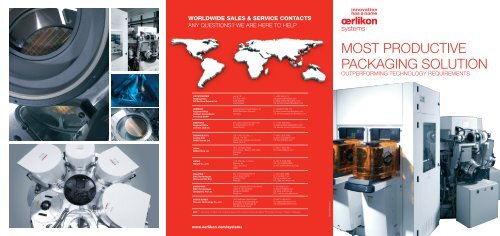
worldwide sales & service contacts<br />
Any Questions? We are here to help<br />
Most Productive<br />
Packaging Solution<br />
Outperforming Technology Requirements<br />
LIECHTENSTEIN<br />
Headquarters<br />
OC <strong>Oerlikon</strong> Balzers Ltd.<br />
Iramali 18<br />
P.O. Box 1000<br />
9496 Balzers<br />
Liechtenstein<br />
T: +423 388 4770<br />
info.systems@oerlikon.com<br />
S: sales.systems@oerlikon.com<br />
CS: service.systems@oerlikon.com<br />
Germany<br />
Regional Office<br />
<strong>Oerlikon</strong> Deutschland<br />
Vertriebs GmbH<br />
Karl-Hammerschmidt-Strasse 34<br />
85609 Aschheim-Dornach<br />
Germany<br />
T: +49 89 75 505 100<br />
S: sales.systems.mn@oerlikon.com<br />
CS: service.systems.mn@oerlikon.com<br />
AMERICAS<br />
Regional Office<br />
<strong>Oerlikon</strong> USA Inc<br />
970 Lake Carillion Dr, Suite 300<br />
St. Petersburg FL 33716<br />
United States<br />
T: +1 887 948 0260<br />
S: sales.systems.sp@oerlikon.com<br />
CS: service.systems.sp@oerlikon.com<br />
Taiwan (R.O.C.)<br />
Central Hub<br />
DKSH Taiwan Ltd.<br />
China<br />
DKSH China Ltd.<br />
13F-1, No.100, Sec. 1,<br />
Jiafong 11th Rd.<br />
Jhubei City, Hsinchu County 302<br />
Taiwan (R.O.C.)<br />
1801 Hongmei Road<br />
Innov Tower / Block A Unit 2208<br />
Shanghai<br />
China<br />
T: +886 3 657 8788<br />
S: jason.chen@dksh.com<br />
CS: ben.lin@dksh.com<br />
T: +86 21 5383 8811<br />
S: christy.liu@dksh.com<br />
Japan<br />
Hakuto Co., Ltd.<br />
1-13. Shinjuku 1-Chome<br />
Shinjuku-ku<br />
Tokyo 160-8910<br />
Japan<br />
S: +81-3-3225-8992<br />
CS: +81-3-3225-8992<br />
S: HKT-oerlikon@hakuto.co.jp<br />
Malaysia *<br />
ZMC Technologies<br />
(Malaysia) Sdn Bhd<br />
No. 1-3-23 Krystal Point 2<br />
Lebuh Bukit Kecil 6<br />
Penang 11900<br />
Malaysia<br />
T: +60 4 646 4586<br />
S: yf_lau@zmc.net<br />
CS: pf_lau@zmc.net<br />
STL: julie_khoo@zmc.net<br />
Singapore *<br />
ZMC Technologies<br />
(Singapore) Pte Ltd<br />
10 Ubi Crescent #05-92/93/94/95<br />
Lobby E, Ubi Techpark<br />
Singapore 408564<br />
Singapore<br />
T: +65 6285 1161<br />
S: steven_ho@zmc.net<br />
CS: jiang_ez@zmc.net<br />
STL: carmen_leong@zmc.net<br />
South Korea<br />
Woowon Technology Co., Ltd<br />
1903 Parkview Office Tower<br />
6 Jeongja-dong, Bundang-gu<br />
Seongnam-si, Kyeonggi-do<br />
463-863 South Korea<br />
T: +82 31 783 4770<br />
S: hongson@wwtech.co.kr<br />
CS: harrylee@wwtech.co.kr<br />
KEY: T: Telephone, S: Sales, CS: Customer service, STL: Support, training & logistics. *Including Indonesia / Thailand / Philippines<br />
HEX/6P/EN/06_2012<br />
www.oerlikon.com/systems
HEXAGON<br />
Advanced packaging sputtering solution for high volume production<br />
HEXAGON<br />
Applications<br />
HEXAGON<br />
Technical Information<br />
Innovation has a name –<br />
Cost of ownership does too<br />
At <strong>Oerlikon</strong>, we understand the pressure you<br />
have to lower your cost per wafer. That’s why our<br />
newest tool for advanced packaging more than<br />
doubles wafer throughput, has a 50% smaller<br />
footprint than its competitors, and runs up to<br />
5’000 wafers before requiring maintenance.<br />
The revolving<br />
carousel on HEXAGON<br />
Productivity<br />
Features<br />
Under Bump & Re-distribution Metallization<br />
Throughput<br />
Footprint & Layout<br />
Cost per Wafer<br />
J J<br />
Highest throughput<br />
JJ<br />
Smallest footprint<br />
JJ<br />
Lowest energy consumption<br />
Reliability<br />
J J<br />
Proven process components<br />
J J<br />
Proven material handling systems<br />
J J<br />
Proven control backbone<br />
Availability<br />
J J<br />
Designed for processing organic passivated wafers<br />
300mm or 200/300mm Bridge Capability<br />
Process Capabilities<br />
JJ<br />
Thermal pre-treatment (Degas)<br />
JJ<br />
Low temperature ICP etching<br />
JJ<br />
DC/DC-pulsed sputtering<br />
JJ<br />
Fast wafer transfer to minimize contamination<br />
Process Chambers<br />
JJ<br />
Integrated stainless steel process chambers<br />
JJ<br />
Full process isolation<br />
JJ<br />
UHV pumping and vacuum capability<br />
JJ<br />
JJ<br />
JJ<br />
JJ<br />
System integration and packaging are responsible for the functionality,<br />
quality and economy of microelectronic products.<br />
UBM and RDL films like Ti-Cu, WTi-Cu, Ti- NiV- Cu etc. are commonly used<br />
in todays advanced packaging industry. The HEXAGON provides:<br />
JJ<br />
Low contact resistance<br />
JJ<br />
No damage ICP etching<br />
JJ<br />
Good adhesion to the chip surface<br />
JJ<br />
Low stress metal stack<br />
HEXAGON is the ideal solution for the latest generation ICs,<br />
organic passivated- or reconstituted (mold) wafers<br />
<strong>Oerlikon</strong> is the market leader in UBM and RDL metallization<br />
JJ<br />
JJ<br />
70 wafers-per-hour (Wph) handling limit<br />
UBM processing with BKM (20nm Etch): 60 Wph<br />
Productivity<br />
JJ<br />
JJ<br />
JJ<br />
Over 85% typical availability<br />
Up to 5’000 wafers maintenance intervals<br />
Less than 6 hours total equipment maintenance time<br />
JJ<br />
Breakage rate less than 1:20’000<br />
JJ<br />
Meantime between failure over 500 hours<br />
JJ<br />
JJ<br />
JJ<br />
12m 2 equipment mainframe<br />
5m 2 support and control systems<br />
17m 2 total installation area<br />
Less than half of any other<br />
commercially available system<br />
J J<br />
Highest wafer output per maintenance interval<br />
J J<br />
Temperature controlled process chambers<br />
Maintainability<br />
J J<br />
Drop-in shield kits<br />
J J<br />
Powered source handling<br />
J J<br />
Automated maintenance services<br />
Chucks<br />
JJ<br />
Temperature controlled (heated or cooled)<br />
JJ<br />
Full face, clamped, ESC, floating<br />
JJ<br />
RF or DC biased<br />
Transfer System<br />
JJ<br />
Up to four FOUP atmospheric front end stations<br />
JJ<br />
High throughput synchronous motion indexer<br />
JJ<br />
Wafer position monitoring<br />
JJ<br />
Mechanically confined wafer transfers<br />
J J<br />
Cryogenic gates and toroidal chamber design<br />
Thin Wafer & Backside Metallization<br />
JJ<br />
JJ<br />
JJ<br />
Backside metallization with up to 4 metals on thin wafers is typically used for power<br />
devices, micro-processors, graphic chips, TSV wafers etc. Very thin wafers are<br />
typically bonded to a glass carrier, alternatively the TAIKO ® grinding process provides<br />
enhanced stability for very thin wafers.<br />
Handling reliability for thin wafers is one of the key advantages of the HEXAGON<br />
<strong>Oerlikon</strong> is the market leader in backside metallization<br />
Below: At just 12m 2 the HEXAGON mainframe<br />
for open source isolation<br />
Operability<br />
JJ<br />
Fully pre-integrated systems for fast installation<br />
JJ<br />
High spare part overlap with previous generation<br />
J J<br />
> 90% process matching with previous generation<br />
J J<br />
> 90% control and operation compatibility<br />
with previous generation<br />
HEXAGON<br />
HEXAGON