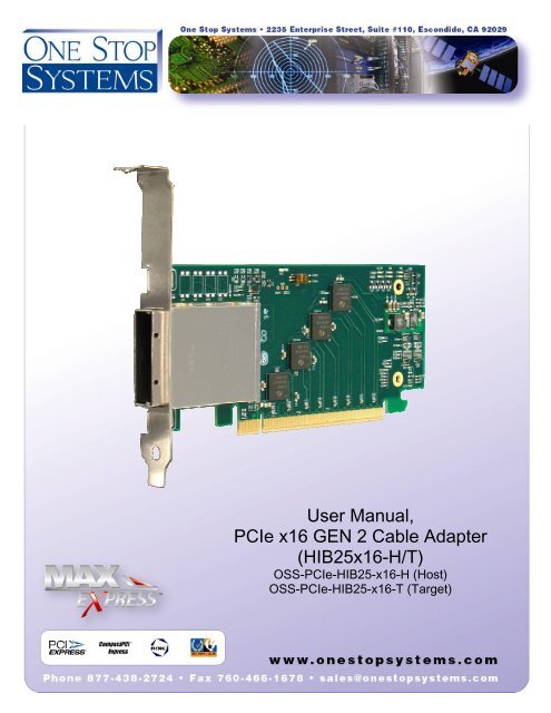
User Manual, PCIe x16 GEN 2 Cable Adapter - One Stop Systems, Inc.
User Manual, PCIe x16 GEN 2 Cable Adapter - One Stop Systems, Inc.
User Manual, PCIe x16 GEN 2 Cable Adapter - One Stop Systems, Inc.
- No tags were found...

You also want an ePaper? Increase the reach of your titles
YUMPU automatically turns print PDFs into web optimized ePapers that Google loves.
<strong>User</strong> <strong>Manual</strong>,<br />
<strong>PCIe</strong> <strong>x16</strong> <strong>GEN</strong> 2 <strong>Cable</strong> <strong>Adapter</strong><br />
(HIB25<strong>x16</strong>-H/T)<br />
OSS-<strong>PCIe</strong>-HIB25-<strong>x16</strong>-H (Host)<br />
OSS-<strong>PCIe</strong>-HIB25-<strong>x16</strong>-T (Target)
Table of Contents<br />
1 Overview<br />
1.a. Host cable adapter ................................................................................................................................3<br />
1.b. Target cable adapter .............................................................................................................................3<br />
1.c. Specifications ........................................................................................................................................4<br />
1.d. Block diagram........................................................................................................................................4<br />
2. Initial set-up<br />
2.a. Unpacking instructions ..........................................................................................................................5<br />
2.b. Installing the host cable adapter............................................................................................................5<br />
2.c. Removing the host cable adapter ..........................................................................................................6<br />
2.d. When using with any third party I/O device ...........................................................................................6<br />
3. Signal adjustment<br />
3.a. Signal adjustment..................................................................................................................................7<br />
5. Ordering Information<br />
6. Appendix<br />
<strong>One</strong> <strong>Stop</strong> <strong>Systems</strong><br />
OSS-<strong>PCIe</strong>-HIB25-<strong>x16</strong>-H/T<br />
Rev. A Page 2
1. Overview<br />
2.a. Host cable adapter<br />
The host adapter is installed into the host computer’s <strong>PCIe</strong> <strong>x16</strong> slot. The host cable adapter (Part # OSS-<strong>PCIe</strong>-HIB25-<strong>x16</strong>-H)<br />
allows communication between a processor and an I/O point.<br />
Slot Cover<br />
(Also<br />
available in<br />
low profile<br />
height)<br />
<strong>PCIe</strong><br />
<strong>x16</strong>Connector<br />
2.b. Target cable adapter<br />
The target cable adapter (Part# OSS-<strong>PCIe</strong>-HIB25-<strong>x16</strong>-T) fits into an OSS custom 2-slot backplane and extends the <strong>PCIe</strong><br />
bus to a single add-in board via a <strong>PCIe</strong> <strong>x16</strong> cable.<br />
Note: This area is populated on target<br />
board<br />
<strong>One</strong> <strong>Stop</strong> <strong>Systems</strong><br />
OSS-<strong>PCIe</strong>-HIB25-<strong>x16</strong>-H/T<br />
Rev. A Page 3
1.a. Specifications<br />
Dimensions (H x L): 2.2 x 4.5 inches (55 x 114mm)<br />
Front Panel Connectors: <strong>One</strong> <strong>PCIe</strong> <strong>x16</strong> cable connector<br />
Front Panel Indicators: Power On / <strong>Cable</strong> Present LEDs<br />
Power Consumption (designed to meet the following conditions) 3.75W typical, 3.3V@1.3A<br />
Operating Environment (designed to meet the following conditions)<br />
Temperature Range: 0° to 50°C (32° to 122°F)<br />
Relative Humidity: 10 to 90% non-condensing<br />
Shock: 30g acceleration peak (11ms pulse)<br />
Vibration: 5-17 Hz 0.5” double amplitude displacement; 7-2000Hz, 1.5g acceleration.<br />
Redriver: Pericom PI2EQX5804<br />
Agency Compliance: UL60950.FCC Class B, CE safety and emissions<br />
1.b. Block Diagram<br />
Clock*<br />
X16 <strong>PCIe</strong><br />
Tx<br />
LVPECL<br />
Clock Buffer<br />
<strong>PCIe</strong> Signal<br />
Redriver<br />
Clock*<br />
X16 <strong>PCIe</strong><br />
Tx<br />
X16 <strong>PCIe</strong> Rx<br />
<strong>PCIe</strong> Signal<br />
Redriver<br />
X16 <strong>PCIe</strong> Rx<br />
CPRSNT#<br />
+3.3v<br />
Downstream<br />
X16 PCI Express<br />
<strong>Cable</strong> Connector<br />
LEDs<br />
<strong>Cable</strong> Present/ Pwr<br />
LEDs<br />
<strong>PCIe</strong> lane status<br />
*Clock direction shown in Host configuration<br />
Upstream<br />
X16 PCI Express<br />
Card Edge Connector<br />
<strong>One</strong> <strong>Stop</strong> <strong>Systems</strong><br />
OSS-<strong>PCIe</strong>-HIB25-<strong>x16</strong>-H/T<br />
Rev. A Page 4
2. Initial Set-Up<br />
2.a. Unpacking Instructions<br />
1) If the carton is damaged when you receive it, request that the carrier’s agent be present when you unpack and inspect<br />
the equipment.<br />
2) After unpacking, verify that all items listed in the packing list are present.<br />
3) Inspect the equipment for shipping damage.<br />
4) Save all packing material for storage or return shipment of the equipment.<br />
Installation and Removal<br />
1) Power down the host system.<br />
2) Open the chassis according to your system documentation.<br />
3) Remove the Host <strong>Cable</strong> <strong>Adapter</strong> from the protective bag, observing proper ESD safety procedures.<br />
2.b. Installing the Host <strong>Cable</strong> <strong>Adapter</strong>:<br />
1) Insert the Host <strong>Cable</strong> <strong>Adapter</strong> into a <strong>PCIe</strong> <strong>x16</strong> add-in card slot. Make sure that the card is well seated and tighten the<br />
screw.<br />
2) Attach the cable by first pulling back on the retractor ring. With the keyed slot aligned with the connector key ridge on<br />
the slot cover, insert the cable connector into the cable shell on the board until the connector teeth snap<br />
securely into the holes in the cable shell.<br />
3) The connectors on either end of the <strong>PCIe</strong> <strong>x16</strong> cable are identical. Each connector is equipped with a retractor to allow<br />
the connector to be locked into place.<br />
<strong>One</strong> <strong>Stop</strong> <strong>Systems</strong><br />
OSS-<strong>PCIe</strong>-HIB25-<strong>x16</strong>-H/T<br />
Rev. A Page 5
2.c. Removing the Host <strong>Cable</strong> <strong>Adapter</strong><br />
1) To remove cable pull back on green thumb tab to release metal pins and gently separate.<br />
2) Loosen and remove the screw before removing the Host <strong>Cable</strong> <strong>Adapter</strong> from the card slot.<br />
2.d. When using with any third party I/O device:<br />
1) Install the downstream board into the appropriate <strong>PCIe</strong> slot.<br />
2) Connect the external power source (separate from the host system power supply) to the downstream device if<br />
necessary.<br />
3) Connect the <strong>PCIe</strong> cable to both the upstream host adapter and the downstream device.<br />
<strong>One</strong> <strong>Stop</strong> <strong>Systems</strong><br />
OSS-<strong>PCIe</strong>-HIB25-<strong>x16</strong>-H/T<br />
Rev. A Page 6
3. Signal Adjustment<br />
3.a. Signal Adjustment<br />
The following chart indicates the default settings for the signal equalization.<br />
SEL_2[A:D] SEL_1[A:D] SEL_0[A:D] @1.25GHZ @2.5GHZ<br />
0 0 0 0.5dB 1.2dB<br />
0 0 1 0.6dB 1.5dB<br />
0 1 0 1.0dB 2.6dB<br />
0 1 1 1.9dB 4.3dB<br />
1 0 0 2.8dB 5.8dB<br />
1 0 1 3.6dB 7.1dB<br />
1 1 0 5.0dB 9.0dB<br />
1 1 1 7.7dB 12.3dB<br />
Edge<br />
Default<br />
<strong>Cable</strong><br />
Default<br />
Table 1: Equalizer Selection (refer to call-out on photo)<br />
The following chart indicates the default settings of the 2-position dip switches for output swing control.<br />
S_1[A:D] S_0[A:D] Swing (Diff. VPP)<br />
0 0 1V<br />
0 1 05V<br />
1 0 0.7V<br />
1 1 0.9V<br />
<strong>Cable</strong><br />
Default<br />
Edge<br />
Default<br />
Table 2: Output Swing Control (refer to call-out on photo)<br />
The following chart indicates the default setting for de-emphasis adjustment<br />
D2_[A:D] D1_[A:D] D0_[A;D] De-emphasis<br />
0 0 0 0dB<br />
0 0 1 -2.5dB<br />
0 1 0 -3.5dB<br />
0 1 1 -4.5dB<br />
1 0 0 -5.5dB<br />
1 0 1 -6.5dB<br />
1 1 0 -7.5dB<br />
1 1 1 -8.5dB<br />
SW=ON<br />
Default<br />
SW=OFF<br />
Default<br />
Table 3: De-emphasis Adjustment (refer to call-out on photo)<br />
<strong>One</strong> <strong>Stop</strong> <strong>Systems</strong><br />
OSS-<strong>PCIe</strong>-HIB25-<strong>x16</strong>-H/T<br />
Rev. A Page 7
4. Ordering Information<br />
OSS - <strong>PCIe</strong>-HIB25-<strong>x16</strong> - H - <strong>One</strong> <strong>Stop</strong> <strong>Systems</strong> HIB25<strong>x16</strong> host cable adapter.<br />
OSS - <strong>PCIe</strong>-HIB25-<strong>x16</strong> - T - <strong>One</strong> <strong>Stop</strong> <strong>Systems</strong> HIB25<strong>x16</strong> host cable adapter.<br />
<strong>One</strong> <strong>Stop</strong> <strong>Systems</strong><br />
OSS-<strong>PCIe</strong>-HIB25-<strong>x16</strong>-H/T<br />
Rev. A Page 8
Appendix<br />
4.c. Pin Assignments<br />
Connectors <strong>PCIe</strong> <strong>x16</strong> Card Edge Connector<br />
• The pins are numbered as shown with side A on the top of the centerline on the solder side of the board and side B on the<br />
bottom of the centerline on the component side of the board.<br />
• The <strong>PCIe</strong> interface pins PETpx, PETnx, PERpx, and PERnx are named with the following convention: “PE” stands for <strong>PCIe</strong><br />
high speed, “T” for Transmitter, “R” for Receiver, “p” for positive (+), and “n” for negative (-).<br />
• Note that adjacent differential pairs are separated by two ground pins to manage the connector crosstalk.<br />
Table 1: Pin-out for the <strong>PCIe</strong> <strong>x16</strong> Card Edge Connector on the Host <strong>Cable</strong> <strong>Adapter</strong><br />
Side B<br />
Side A<br />
Pin #<br />
Name Description Name Description<br />
1 N/C N/C PRSNT1# Hot-Plug presence detect<br />
2 N/C N/C N/C N/C<br />
3 N/C N/C N/C N/C<br />
4 GND Ground GND Ground<br />
5 NC N/C N/C Not connected<br />
6 N/C N/C JTAG3 TDI (Test Data Input)<br />
7 GND Ground JTAG4 TDO (Test Data Output)<br />
8 +3.3V 3.3 V power N/C Not connected<br />
9 N/C Not connected N/C Not connected<br />
10 3.3Vaux 3.3 V auxiliary power +3.3V 3.3 V power<br />
11 N/C N/C PERST# Fundamental reset<br />
Mechanical key<br />
12 RSVD Reserved GND Ground<br />
13 GND Ground REFCLK+<br />
Reference clock (differential<br />
14 PETp0 REFCLK pair)<br />
Transmitter differential pair,<br />
15 PETn0 Lane 0 GND Ground<br />
16 GND Ground PERp0<br />
17 PRSNT2# Hot-Plug presence detect PERn0<br />
Receiver differential pair, Lane 0<br />
18 GND Ground GND Ground<br />
19 PETp1 RSVD Reserved<br />
Transmitter differential pair,<br />
20 PETn1 Lane 1 GND Ground<br />
21 GND Ground PERp1<br />
22 GND Ground PERn1<br />
Receiver differential pair, Lane 1<br />
23 PETp2 GND Ground<br />
Transmitter differential pair,<br />
24 PETn2 Lane 2 GND Ground<br />
25 GND Ground PERp2<br />
26 GND Ground PERn2<br />
Receiver differential pair, Lane 2<br />
<strong>One</strong> <strong>Stop</strong> <strong>Systems</strong><br />
OSS-<strong>PCIe</strong>-HIB25-<strong>x16</strong>-H/T<br />
Rev. A Page 9
27 PETp3 GND Ground<br />
Transmitter differential pair,<br />
28 PETn3 Lane 3 GND Ground<br />
29 GND Ground PERp3<br />
30 RSVD Reserved PERn3<br />
31 PRSNT2# Hot-Plug presence detect GND Ground<br />
32 GND Ground RSVD Reserved<br />
Receiver differential pair, Lane 3<br />
Notes:<br />
1 Optional signals that are not implemented are to be left as no connects on the board side connector.<br />
2 Reserved signals must be left as no connects on the board side connector.<br />
3 Although support of CWAKE# is optional from the board side connector perspective, an allocated wire is mandated for the cable<br />
assembly.<br />
4 Board side pin-out on both sides of the Link is identical. The cable assembly incorporates a null modem for the <strong>PCIe</strong> transmit and<br />
receive pairs.<br />
PCI Express <strong>x16</strong> Connector Pin Assignment<br />
Row B, Pin 19<br />
Row A, Pin 1<br />
PIN- out for the <strong>PCIe</strong> <strong>x16</strong> <strong>Cable</strong><br />
Pin # <strong>Cable</strong> Side 1 <strong>Cable</strong> Side 2 Pin #<br />
A1 A4 A7 A10 A13<br />
A16 B1 B4 B7 B10<br />
B13<br />
GND Drain Wires GND A1 A4 A7 A10 A13<br />
A16 B1 B4 B7 B10<br />
B13<br />
A2 PETp0 Differential Pair PERp0 B2<br />
A3 PETn0 PERn0 B3<br />
A5 PETp1 Differential Pair PERp1 B5<br />
A6 PETn1<br />
PERn1<br />
B6<br />
Pin # <strong>Cable</strong> Side 1 <strong>Cable</strong> Side 2 Pin #<br />
A8 PETp2 Differential Pair PERp2 B8<br />
A9 PETn2 PERn2 B9<br />
A11 PETp3 Differential Pair PERp3 B11<br />
A12 PETn3 PERn3 B12<br />
A14 CREFCLK+ Differential Pair CREFCLK+ A14<br />
A15 CREFCLK CREFCLK- A15<br />
A17 SB_RTN Hook-up Wire SB_RTN A17<br />
<strong>One</strong> <strong>Stop</strong> <strong>Systems</strong><br />
OSS-<strong>PCIe</strong>-HIB25-<strong>x16</strong>-H/T<br />
Rev. A Page 10
A18 CPRSNT# Hook-up Wire CPRSNT# A18<br />
A19 CPWRON Hook-up Wire CPWRON A19<br />
B2 PERp0 Differential Pair PETp0 A2<br />
B3 PERn0 PETn0 A3<br />
B5 PERp1 Differential Pair PETp1 A5<br />
B6 PERn1 PETn1 A6<br />
B8 PERp2 Differential Pair PETp2 A8<br />
B9 PERn2 PETn2 A9<br />
B11 PERp3 Differential Pair PETp3 A11<br />
B12 PERn3 PETn3 A12<br />
B14 PWR NC PWR B14<br />
B15 PWR NC PWR B15<br />
B16 PWR_RTN NC PWR_RTN B16<br />
B17 PWR_RTN NC PWR_RTN B17<br />
B18 CWAKE# Hook-up Wire CWAKE# B18<br />
B19 CPERST# Hook-up Wire CPERST# B19<br />
Back shell Chassis Ground<br />
Overall <strong>Cable</strong><br />
Braid<br />
Chassis Ground Back shell<br />
Signal Descriptions<br />
PETp(x)<br />
PETn(x)<br />
PERp(x)<br />
PERn(x)<br />
CREFCLK+/-<br />
SB_RTN<br />
CPRSNT#<br />
PWR<br />
PWR_RTN<br />
CWAKE#<br />
CPERST#<br />
PCI Express Transmit Positive signal of (x) pair.<br />
PCI Express Transmit Negative signal of (x) pair.<br />
PCI Express Receive Positive signal of (x) pair.<br />
PCI Express Receive Negative signal of (x) pair.<br />
<strong>Cable</strong> REFerence CLocK: Provides a reference clock from the host system to the<br />
remote system.<br />
Side Band ReTurN: return path for single ended signals from remote systems.<br />
<strong>Cable</strong> PReSeNT: Indicates the presence of a device beyond the cable.<br />
PoWeR: Provides local power for in-cable redriver circuits. Only needed on long<br />
cables. Power does not go across the cable.)<br />
PoWeR ReTurN: Provides local power return path for PWR pins.<br />
<strong>Cable</strong> WAKE<br />
<strong>Cable</strong> PCI Express Reset<br />
<strong>One</strong> <strong>Stop</strong> <strong>Systems</strong><br />
OSS-<strong>PCIe</strong>-HIB25-<strong>x16</strong>-H/T<br />
Rev. A Page 11