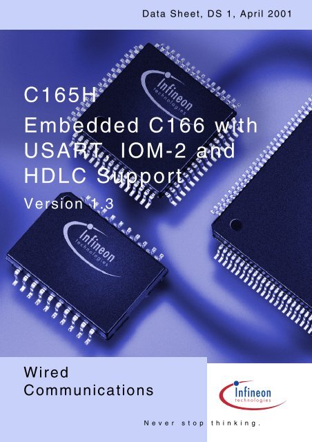
C165H Embedded C166 with USART, IOM-2 and HDLC Support
C165H Embedded C166 with USART, IOM-2 and HDLC Support
C165H Embedded C166 with USART, IOM-2 and HDLC Support

You also want an ePaper? Increase the reach of your titles
YUMPU automatically turns print PDFs into web optimized ePapers that Google loves.
Data Sheet, DS 1, April 2001<br />
<strong>C165H</strong><br />
<strong>Embedded</strong> <strong>C166</strong> <strong>with</strong><br />
<strong>USART</strong>, <strong>IOM</strong>-2 <strong>and</strong><br />
<strong>HDLC</strong> <strong>Support</strong><br />
Version 1.3<br />
Wired<br />
Communications<br />
Never stop thinking.
Edition 2001-04-01<br />
Published by Infineon Technologies AG,<br />
St.-Martin-Strasse 53,<br />
D-81541 München, Germany<br />
© Infineon Technologies AG 2001.<br />
All Rights Reserved.<br />
Attention please!<br />
The information herein is given to describe certain components <strong>and</strong> shall not be considered as warranted<br />
characteristics.<br />
Terms of delivery <strong>and</strong> rights to technical change reserved.<br />
We hereby disclaim any <strong>and</strong> all warranties, including but not limited to warranties of non-infringement, regarding<br />
circuits, descriptions <strong>and</strong> charts stated herein.<br />
Infineon Technologies is an approved CECC manufacturer.<br />
Information<br />
For further information on technology, delivery terms <strong>and</strong> conditions <strong>and</strong> prices please contact your nearest<br />
Infineon Technologies Office in Germany or our Infineon Technologies Representatives worldwide (see address<br />
list).<br />
Warnings<br />
Due to technical requirements components may contain dangerous substances. For information on the types in<br />
question please contact your nearest Infineon Technologies Office.<br />
Infineon Technologies Components may only be used in life-support devices or systems <strong>with</strong> the express written<br />
approval of Infineon Technologies, if a failure of such components can reasonably be expected to cause the failure<br />
of that life-support device or system, or to affect the safety or effectiveness of that device or system. Life support<br />
devices or systems are intended to be implanted in the human body, or to support <strong>and</strong>/or maintain <strong>and</strong> sustain<br />
<strong>and</strong>/or protect human life. If they fail, it is reasonable to assume that the health of the user or other persons may<br />
be endangered.
Data Sheet, DS 1, April 2001<br />
<strong>C165H</strong><br />
<strong>Embedded</strong> <strong>C166</strong> <strong>with</strong><br />
<strong>USART</strong>, <strong>IOM</strong>-2 <strong>and</strong><br />
<strong>HDLC</strong> <strong>Support</strong><br />
Version 1.3<br />
Wired<br />
Communications<br />
Never stop thinking.
<strong>C165H</strong><br />
Revision History: 2001-04-01 DS 1<br />
Previous Version: This is the first non-preliminary version. 1)<br />
Page Subjects (major changes since last revision)<br />
1) All previous distributed versions are preliminary. They have been replaced by this version.<br />
For questions on technology, delivery <strong>and</strong> prices please contact the Infineon<br />
Technologies Offices in Germany or the Infineon Technologies Companies <strong>and</strong><br />
Representatives worldwide: see our webpage at http://www.infineon.com
<strong>C165H</strong><br />
Table of Contents<br />
Page<br />
1 Overview . . . . . . . . . . . . . . . . . . . . . . . . . . . . . . . . . . . . . . . . . . . . . . . . . . 11<br />
1.1 Key Features . . . . . . . . . . . . . . . . . . . . . . . . . . . . . . . . . . . . . . . . . . . . . . . 12<br />
1.2 Logic Symbol . . . . . . . . . . . . . . . . . . . . . . . . . . . . . . . . . . . . . . . . . . . . . . . 15<br />
1.3 Pinning Diagram . . . . . . . . . . . . . . . . . . . . . . . . . . . . . . . . . . . . . . . . . . . . 16<br />
1.4 Typical Applications . . . . . . . . . . . . . . . . . . . . . . . . . . . . . . . . . . . . . . . . . . 17<br />
1.4.1 ISDN NT <strong>and</strong> PBX Applications . . . . . . . . . . . . . . . . . . . . . . . . . . . . . . . 17<br />
2 Pin Descriptions . . . . . . . . . . . . . . . . . . . . . . . . . . . . . . . . . . . . . . . . . . . 18<br />
2.1 <strong>C165H</strong> Pin Diagram . . . . . . . . . . . . . . . . . . . . . . . . . . . . . . . . . . . . . . . . . . 18<br />
2.2 <strong>C165H</strong> Pin Definitions <strong>and</strong> Functions . . . . . . . . . . . . . . . . . . . . . . . . . . . . 19<br />
3 Architectural Overview . . . . . . . . . . . . . . . . . . . . . . . . . . . . . . . . . . . . . . 28<br />
3.1 Basic CPU Concepts <strong>and</strong> Optimizations . . . . . . . . . . . . . . . . . . . . . . . . . . 29<br />
3.2 On-Chip System Resources . . . . . . . . . . . . . . . . . . . . . . . . . . . . . . . . . . . 34<br />
3.3 Clock Generation Concept . . . . . . . . . . . . . . . . . . . . . . . . . . . . . . . . . . . . . 36<br />
3.4 On-Chip Peripheral Blocks . . . . . . . . . . . . . . . . . . . . . . . . . . . . . . . . . . . . 40<br />
3.5 Protected Bits . . . . . . . . . . . . . . . . . . . . . . . . . . . . . . . . . . . . . . . . . . . . . . 44<br />
4 Memory Organization . . . . . . . . . . . . . . . . . . . . . . . . . . . . . . . . . . . . . . . 46<br />
4.1 Internal RAM <strong>and</strong> SFR Area . . . . . . . . . . . . . . . . . . . . . . . . . . . . . . . . . . 48<br />
4.2 External Memory Space . . . . . . . . . . . . . . . . . . . . . . . . . . . . . . . . . . . . . 53<br />
4.3 Crossing Memory Boundaries . . . . . . . . . . . . . . . . . . . . . . . . . . . . . . . . . 54<br />
5 Central Processor Unit . . . . . . . . . . . . . . . . . . . . . . . . . . . . . . . . . . . . . . 55<br />
5.1 Instruction Pipelining . . . . . . . . . . . . . . . . . . . . . . . . . . . . . . . . . . . . . . . . . 57<br />
5.2 Bit-H<strong>and</strong>ling <strong>and</strong> Bit-Protection . . . . . . . . . . . . . . . . . . . . . . . . . . . . . . . . . 63<br />
5.3 Instruction State Times . . . . . . . . . . . . . . . . . . . . . . . . . . . . . . . . . . . . . . . 64<br />
5.4 CPU Special Function Registers . . . . . . . . . . . . . . . . . . . . . . . . . . . . . . . . 65<br />
5.5 PEC - Extension of Functionality . . . . . . . . . . . . . . . . . . . . . . . . . . . . . . . . 84<br />
6 Interrupt <strong>and</strong> Trap Functions . . . . . . . . . . . . . . . . . . . . . . . . . . . . . . . . . 92<br />
6.1 Interrupt System Structure . . . . . . . . . . . . . . . . . . . . . . . . . . . . . . . . . . . . . 93<br />
6.2 Interrupt Control Registers . . . . . . . . . . . . . . . . . . . . . . . . . . . . . . . . . . . . . 98<br />
6.3 Operation of the PEC Channels . . . . . . . . . . . . . . . . . . . . . . . . . . . . . . . 103<br />
6.4 Prioritization of Interrupt <strong>and</strong> PEC Service Requests . . . . . . . . . . . . . . . 105<br />
6.5 Saving the Status during Interrupt Service . . . . . . . . . . . . . . . . . . . . . . . 108<br />
6.6 Interrupt Response Times . . . . . . . . . . . . . . . . . . . . . . . . . . . . . . . . . . . . 109<br />
6.7 PEC Response Times . . . . . . . . . . . . . . . . . . . . . . . . . . . . . . . . . . . . . . 112<br />
6.8 External Interrupts . . . . . . . . . . . . . . . . . . . . . . . . . . . . . . . . . . . . . . . . . . 113<br />
6.8.1 Fast External Interrupts . . . . . . . . . . . . . . . . . . . . . . . . . . . . . . . . . . . . 115<br />
6.8.2 External Interrupt Source Control . . . . . . . . . . . . . . . . . . . . . . . . . . . . 115<br />
6.8.3 Interrupt Subnode Control . . . . . . . . . . . . . . . . . . . . . . . . . . . . . . . . . . 117<br />
6.8.4 The Interrupt Control Register . . . . . . . . . . . . . . . . . . . . . . . . . . . . . . . 118<br />
6.9 Trap Functions . . . . . . . . . . . . . . . . . . . . . . . . . . . . . . . . . . . . . . . . . . . . . 119<br />
Data Sheet 2001-04-19
<strong>C165H</strong><br />
Table of Contents<br />
Page<br />
7 Parallel Ports . . . . . . . . . . . . . . . . . . . . . . . . . . . . . . . . . . . . . . . . . . . . . 124<br />
7.1 PORT0 . . . . . . . . . . . . . . . . . . . . . . . . . . . . . . . . . . . . . . . . . . . . . . . . . . . 127<br />
7.1.1 Alternate Functions of PORT0 . . . . . . . . . . . . . . . . . . . . . . . . . . . . . . . 132<br />
7.2 PORT1 . . . . . . . . . . . . . . . . . . . . . . . . . . . . . . . . . . . . . . . . . . . . . . . . . . . 134<br />
7.2.1 Alternate Functions of PORT1 . . . . . . . . . . . . . . . . . . . . . . . . . . . . . . . 138<br />
7.3 PORT2 . . . . . . . . . . . . . . . . . . . . . . . . . . . . . . . . . . . . . . . . . . . . . . . . . . . 139<br />
7.3.1 Alternate Functions of PORT2 . . . . . . . . . . . . . . . . . . . . . . . . . . . . . . . 142<br />
7.4 PORT3 . . . . . . . . . . . . . . . . . . . . . . . . . . . . . . . . . . . . . . . . . . . . . . . . . . . 144<br />
7.4.1 Alternate Functions of PORT3 . . . . . . . . . . . . . . . . . . . . . . . . . . . . . . . 147<br />
7.5 PORT4 . . . . . . . . . . . . . . . . . . . . . . . . . . . . . . . . . . . . . . . . . . . . . . . . . . . 150<br />
7.5.1 Alternate Functions of PORT4 . . . . . . . . . . . . . . . . . . . . . . . . . . . . . . . 153<br />
7.6 PORT6 . . . . . . . . . . . . . . . . . . . . . . . . . . . . . . . . . . . . . . . . . . . . . . . . . . . 154<br />
7.6.1 Alternate Functions of PORT6 . . . . . . . . . . . . . . . . . . . . . . . . . . . . . . . 157<br />
7.7 PORT7 . . . . . . . . . . . . . . . . . . . . . . . . . . . . . . . . . . . . . . . . . . . . . . . . . . . 160<br />
8 Dedicated Pins . . . . . . . . . . . . . . . . . . . . . . . . . . . . . . . . . . . . . . . . . . . . 163<br />
9 External Bus Interface . . . . . . . . . . . . . . . . . . . . . . . . . . . . . . . . . . . . . . 166<br />
9.1 External Bus Modes . . . . . . . . . . . . . . . . . . . . . . . . . . . . . . . . . . . . . . . . . 167<br />
9.2 Programmable Bus Characteristics . . . . . . . . . . . . . . . . . . . . . . . . . . . . . 175<br />
9.3 READY Controlled Bus Cycles . . . . . . . . . . . . . . . . . . . . . . . . . . . . . . . . 181<br />
9.4 Controlling the External Bus Controller . . . . . . . . . . . . . . . . . . . . . . . . . . 183<br />
9.5 EBC Idle State . . . . . . . . . . . . . . . . . . . . . . . . . . . . . . . . . . . . . . . . . . . . . 194<br />
9.6 External Bus Arbitration . . . . . . . . . . . . . . . . . . . . . . . . . . . . . . . . . . . . . . 194<br />
9.7 XBUS Interface . . . . . . . . . . . . . . . . . . . . . . . . . . . . . . . . . . . . . . . . . . . . 198<br />
9.8 Initialization of the <strong>C165H</strong>’s X-peripherals . . . . . . . . . . . . . . . . . . . . . . . . 199<br />
10 General Purpose Timer Unit . . . . . . . . . . . . . . . . . . . . . . . . . . . . . . . . . 200<br />
10.1 Kernel Description . . . . . . . . . . . . . . . . . . . . . . . . . . . . . . . . . . . . . . . . . . 201<br />
10.1.1 Functional Description of Timer Block 1 . . . . . . . . . . . . . . . . . . . . . . . 201<br />
10.1.1.1 Core Timer T3 . . . . . . . . . . . . . . . . . . . . . . . . . . . . . . . . . . . . . . . . . 202<br />
10.1.1.2 Auxiliary Timers T2 <strong>and</strong> T4 . . . . . . . . . . . . . . . . . . . . . . . . . . . . . . . 211<br />
10.1.1.3 Timer Concatenation . . . . . . . . . . . . . . . . . . . . . . . . . . . . . . . . . . . 213<br />
10.1.2 Functional Description of Timer Block 2 . . . . . . . . . . . . . . . . . . . . . . . 218<br />
10.1.2.1 Core Timer T6 . . . . . . . . . . . . . . . . . . . . . . . . . . . . . . . . . . . . . . . . . 219<br />
10.1.2.2 Auxiliary Timer T5 . . . . . . . . . . . . . . . . . . . . . . . . . . . . . . . . . . . . . . 221<br />
10.1.2.3 Timer Concatenation . . . . . . . . . . . . . . . . . . . . . . . . . . . . . . . . . . . 223<br />
10.1.3 GPT Register Set . . . . . . . . . . . . . . . . . . . . . . . . . . . . . . . . . . . . . . . . . 224<br />
11 Asynchronous/Synchr. Serial Interface . . . . . . . . . . . . . . . . . . . . . . . . 238<br />
11.1 Functional Description . . . . . . . . . . . . . . . . . . . . . . . . . . . . . . . . . . . . . . . 238<br />
11.1.1 Features . . . . . . . . . . . . . . . . . . . . . . . . . . . . . . . . . . . . . . . . . . . . . . . . 238<br />
11.1.2 Overview . . . . . . . . . . . . . . . . . . . . . . . . . . . . . . . . . . . . . . . . . . . . . . . 240<br />
11.1.3 Register Description . . . . . . . . . . . . . . . . . . . . . . . . . . . . . . . . . . . . . . 241<br />
11.1.4 General Operation . . . . . . . . . . . . . . . . . . . . . . . . . . . . . . . . . . . . . . . . 252<br />
Data Sheet 2001-04-19
<strong>C165H</strong><br />
Table of Contents<br />
Page<br />
11.1.5 Asynchronous Operation . . . . . . . . . . . . . . . . . . . . . . . . . . . . . . . . . . 253<br />
11.1.5.1 Asynchronous Data Frames . . . . . . . . . . . . . . . . . . . . . . . . . . . . . . 255<br />
11.1.5.2 Asynchronous Transmission . . . . . . . . . . . . . . . . . . . . . . . . . . . . . . 257<br />
11.1.5.3 Asynchronous Reception . . . . . . . . . . . . . . . . . . . . . . . . . . . . . . . . . 257<br />
11.1.5.4 IrDA Mode . . . . . . . . . . . . . . . . . . . . . . . . . . . . . . . . . . . . . . . . . . . . 258<br />
11.1.5.5 RXD/TXD Data Path Selection in Asynchronous Modes . . . . . . . . . 259<br />
11.1.6 Synchronous Operation . . . . . . . . . . . . . . . . . . . . . . . . . . . . . . . . . . . 260<br />
11.1.6.1 Synchronous Transmission . . . . . . . . . . . . . . . . . . . . . . . . . . . . . . . 261<br />
11.1.6.2 Synchronous Reception . . . . . . . . . . . . . . . . . . . . . . . . . . . . . . . . . . 262<br />
11.1.6.3 Synchronous Timing . . . . . . . . . . . . . . . . . . . . . . . . . . . . . . . . . . . . 262<br />
11.1.7 Baudrate Generation . . . . . . . . . . . . . . . . . . . . . . . . . . . . . . . . . . . . . 263<br />
11.1.7.1 Baudrates in Asynchronous Mode . . . . . . . . . . . . . . . . . . . . . . . . . . 264<br />
11.1.7.2 Baudrates in Synchronous Mode . . . . . . . . . . . . . . . . . . . . . . . . . . . 267<br />
11.1.8 Autobaud Detection . . . . . . . . . . . . . . . . . . . . . . . . . . . . . . . . . . . . . . . 269<br />
11.1.8.1 General Operation . . . . . . . . . . . . . . . . . . . . . . . . . . . . . . . . . . . . . . 269<br />
11.1.8.2 Serial Frames for Autobaud Detection . . . . . . . . . . . . . . . . . . . . . . . 270<br />
11.1.8.3 Baudrate Selection <strong>and</strong> Calculation . . . . . . . . . . . . . . . . . . . . . . . . . 272<br />
11.1.8.4 Overwriting Registers on Successful Autobaud Detection . . . . . . . 274<br />
11.1.9 Hardware Error Detection Capabilities . . . . . . . . . . . . . . . . . . . . . . . . 275<br />
11.1.10 Interrupts . . . . . . . . . . . . . . . . . . . . . . . . . . . . . . . . . . . . . . . . . . . . . . . 276<br />
12 Real Time Clock (RTC) . . . . . . . . . . . . . . . . . . . . . . . . . . . . . . . . . . . . . 278<br />
12.1 Introduction . . . . . . . . . . . . . . . . . . . . . . . . . . . . . . . . . . . . . . . . . . . . . . . 278<br />
12.1.1 Features . . . . . . . . . . . . . . . . . . . . . . . . . . . . . . . . . . . . . . . . . . . . . . . . 278<br />
12.1.2 Overview . . . . . . . . . . . . . . . . . . . . . . . . . . . . . . . . . . . . . . . . . . . . . . . 278<br />
12.2 Function Description . . . . . . . . . . . . . . . . . . . . . . . . . . . . . . . . . . . . . . . . 278<br />
12.2.1 RTC Block Diagram . . . . . . . . . . . . . . . . . . . . . . . . . . . . . . . . . . . . . . . 279<br />
12.2.2 RTC Control . . . . . . . . . . . . . . . . . . . . . . . . . . . . . . . . . . . . . . . . . . . . . 280<br />
12.2.3 System Clock Operation . . . . . . . . . . . . . . . . . . . . . . . . . . . . . . . . . . . 280<br />
12.2.4 Cyclic Interrupt Generation . . . . . . . . . . . . . . . . . . . . . . . . . . . . . . . . . 280<br />
12.2.5 Alarm Interrupt Generation . . . . . . . . . . . . . . . . . . . . . . . . . . . . . . . . . 280<br />
12.2.6 48-bit Timer Operation . . . . . . . . . . . . . . . . . . . . . . . . . . . . . . . . . . . . . 281<br />
12.2.7 Defining the RTC Time Base . . . . . . . . . . . . . . . . . . . . . . . . . . . . . . . . 281<br />
12.2.8 Increased RTC Accuracy through Software Correction . . . . . . . . . . . . 283<br />
12.2.9 Hardware dependend RTC Accuracy . . . . . . . . . . . . . . . . . . . . . . . . . 283<br />
12.2.10 Interrupt Sub Node RTCISNC . . . . . . . . . . . . . . . . . . . . . . . . . . . . . . . 283<br />
12.2.11 RTC Disable Functionality . . . . . . . . . . . . . . . . . . . . . . . . . . . . . . . . . . 284<br />
12.2.12 Register Definition of RTC module . . . . . . . . . . . . . . . . . . . . . . . . . . . 285<br />
13 High-Speed Synchronous Serial Interface . . . . . . . . . . . . . . . . . . . . . 290<br />
13.1 Full-Duplex Operation . . . . . . . . . . . . . . . . . . . . . . . . . . . . . . . . . . . . . . 295<br />
13.2 Half Duplex Operation . . . . . . . . . . . . . . . . . . . . . . . . . . . . . . . . . . . . . . 298<br />
13.3 Baud Rate Generation . . . . . . . . . . . . . . . . . . . . . . . . . . . . . . . . . . . . . . 300<br />
13.4 Error Detection Mechanisms . . . . . . . . . . . . . . . . . . . . . . . . . . . . . . . . . 301<br />
Data Sheet 2001-04-19
<strong>C165H</strong><br />
Table of Contents<br />
Page<br />
13.5 SSC Interrupt Control . . . . . . . . . . . . . . . . . . . . . . . . . . . . . . . . . . . . . . . 303<br />
14 <strong>IOM</strong>-2 Interface Controller . . . . . . . . . . . . . . . . . . . . . . . . . . . . . . . . . . . 306<br />
14.1 <strong>IOM</strong>-2 <strong>and</strong> PCM Frame Structure . . . . . . . . . . . . . . . . . . . . . . . . . . . . . . 306<br />
14.1.1 Definitions . . . . . . . . . . . . . . . . . . . . . . . . . . . . . . . . . . . . . . . . . . . . . . 306<br />
14.1.1.1 Frame Structure . . . . . . . . . . . . . . . . . . . . . . . . . . . . . . . . . . . . . . . . 306<br />
14.1.1.2 <strong>HDLC</strong> Channels on the <strong>IOM</strong>-2: B1, B2, D1, D2 . . . . . . . . . . . . . . . . 307<br />
14.1.2 PCM Mode . . . . . . . . . . . . . . . . . . . . . . . . . . . . . . . . . . . . . . . . . . . . . . 307<br />
14.1.3 Terminal Mode . . . . . . . . . . . . . . . . . . . . . . . . . . . . . . . . . . . . . . . . . . . 307<br />
14.1.4 Linecard Mode . . . . . . . . . . . . . . . . . . . . . . . . . . . . . . . . . . . . . . . . . . . 309<br />
14.2 <strong>IOM</strong>-2 H<strong>and</strong>ler . . . . . . . . . . . . . . . . . . . . . . . . . . . . . . . . . . . . . . . . . . . . . 309<br />
14.3 <strong>IOM</strong>-2 Monitor H<strong>and</strong>ler . . . . . . . . . . . . . . . . . . . . . . . . . . . . . . . . . . . . . . 311<br />
14.3.1 H<strong>and</strong>shake Procedure . . . . . . . . . . . . . . . . . . . . . . . . . . . . . . . . . . . . . 311<br />
14.3.2 Abort Procedure . . . . . . . . . . . . . . . . . . . . . . . . . . . . . . . . . . . . . . . . . . 315<br />
14.3.3 MONITOR Interrupt Logic . . . . . . . . . . . . . . . . . . . . . . . . . . . . . . . . . . 317<br />
14.4 C/I Channel H<strong>and</strong>ler . . . . . . . . . . . . . . . . . . . . . . . . . . . . . . . . . . . . . . . . 318<br />
14.4.1 C/I0 - Comm<strong>and</strong>/Indication 0 . . . . . . . . . . . . . . . . . . . . . . . . . . . . . . . . 318<br />
14.4.2 C/I1 - Comm<strong>and</strong>/Indication 1 . . . . . . . . . . . . . . . . . . . . . . . . . . . . . . . . 318<br />
14.4.3 CIC Interrupt Logic . . . . . . . . . . . . . . . . . . . . . . . . . . . . . . . . . . . . . . . . 319<br />
14.4.4 D-Channel Access Control . . . . . . . . . . . . . . . . . . . . . . . . . . . . . . . . . 319<br />
14.4.4.1 TIC Bus D-Channel Access Control for <strong>HDLC</strong>-2 Controller . . . . . . . 320<br />
14.5 Controller Data Access H<strong>and</strong>ler . . . . . . . . . . . . . . . . . . . . . . . . . . . . . . . 321<br />
14.5.1 Description . . . . . . . . . . . . . . . . . . . . . . . . . . . . . . . . . . . . . . . . . . . . . . 322<br />
14.5.2 Looping <strong>and</strong> Shifting Data . . . . . . . . . . . . . . . . . . . . . . . . . . . . . . . . . . 323<br />
14.5.3 Monitoring Data . . . . . . . . . . . . . . . . . . . . . . . . . . . . . . . . . . . . . . . . . . 325<br />
14.5.4 Synchronous Transfer . . . . . . . . . . . . . . . . . . . . . . . . . . . . . . . . . . . . . 326<br />
14.6 Bus Activation / Deactivation (Power Down) . . . . . . . . . . . . . . . . . . . . . . 329<br />
14.6.1 Deactivation Request, Downstream (<strong>C165H</strong>) to Upstream . . . . . . . . . 330<br />
14.6.2 Deactivation, Upstream to Downstream (<strong>C165H</strong>) . . . . . . . . . . . . . . . . 331<br />
14.6.3 Activation Request, Downstream (<strong>C165H</strong>) to Upstream . . . . . . . . . . . 331<br />
14.6.4 Activation, Upstream to Downstream (<strong>C165H</strong>) . . . . . . . . . . . . . . . . . . 331<br />
14.7 <strong>HDLC</strong> Controller . . . . . . . . . . . . . . . . . . . . . . . . . . . . . . . . . . . . . . . . . . . 332<br />
14.7.1 Message Transfer Modes . . . . . . . . . . . . . . . . . . . . . . . . . . . . . . . . . . 333<br />
14.7.1.1 Non-Auto Mode (MDS2-0 = ’01x’) . . . . . . . . . . . . . . . . . . . . . . . . . . 333<br />
14.7.1.2 Transparent Mode 0 (MDS2-0 = ’110’). . . . . . . . . . . . . . . . . . . . . . . 333<br />
14.7.1.3 Transparent Mode 1 (MDS2-0 = ’111’). . . . . . . . . . . . . . . . . . . . . . . 333<br />
14.7.1.4 Transparent Mode 2 (MDS2-0 = ’101’). . . . . . . . . . . . . . . . . . . . . . . 334<br />
14.7.1.5 Extended Transparent Mode (MDS2-0 = ’100’). . . . . . . . . . . . . . . . 334<br />
14.7.2 Data Reception . . . . . . . . . . . . . . . . . . . . . . . . . . . . . . . . . . . . . . . . . . 334<br />
14.7.2.1 General Description . . . . . . . . . . . . . . . . . . . . . . . . . . . . . . . . . . . . . 334<br />
14.7.2.2 Possible Error Conditions during Reception of Frames . . . . . . . . . . 335<br />
14.7.2.3 Receive Frame Structure . . . . . . . . . . . . . . . . . . . . . . . . . . . . . . . . . 335<br />
14.7.3 Data Transmission . . . . . . . . . . . . . . . . . . . . . . . . . . . . . . . . . . . . . . . . 337<br />
Data Sheet 2001-04-19
<strong>C165H</strong><br />
Table of Contents<br />
Page<br />
14.7.3.1 General Description . . . . . . . . . . . . . . . . . . . . . . . . . . . . . . . . . . . . . 337<br />
14.7.3.2 Possible Error Conditions during Transmission of Frames . . . . . . . 339<br />
14.7.3.3 Transmit Frame Structure . . . . . . . . . . . . . . . . . . . . . . . . . . . . . . . . 339<br />
14.7.4 General Access to <strong>IOM</strong>-2 Channels . . . . . . . . . . . . . . . . . . . . . . . . . . 340<br />
14.7.5 Extended Transparent Mode . . . . . . . . . . . . . . . . . . . . . . . . . . . . . . . . 340<br />
14.7.5.1 Transmitter . . . . . . . . . . . . . . . . . . . . . . . . . . . . . . . . . . . . . . . . . . . . 341<br />
14.7.5.2 Receiver . . . . . . . . . . . . . . . . . . . . . . . . . . . . . . . . . . . . . . . . . . . . . . 341<br />
14.7.6 <strong>HDLC</strong> Controller Interrupts . . . . . . . . . . . . . . . . . . . . . . . . . . . . . . . . . 341<br />
14.7.6.1 General <strong>HDLC</strong> Interrupt . . . . . . . . . . . . . . . . . . . . . . . . . . . . . . . . . . 341<br />
14.7.6.2 <strong>HDLC</strong> Transmit/Receive FIFO Interrupt . . . . . . . . . . . . . . . . . . . . . 342<br />
14.7.6.3 Interrupt Generation . . . . . . . . . . . . . . . . . . . . . . . . . . . . . . . . . . . . . 343<br />
14.8 <strong>IOM</strong>-2/<strong>HDLC</strong> Controller Register Set . . . . . . . . . . . . . . . . . . . . . . . . . . . . 343<br />
14.8.1 Register Description Format . . . . . . . . . . . . . . . . . . . . . . . . . . . . . . . . 343<br />
14.8.2 Register Table ordered by Address . . . . . . . . . . . . . . . . . . . . . . . . . . . 344<br />
14.8.3 Detailed Register Description ordered by Address . . . . . . . . . . . . . . . 349<br />
14.8.4 <strong>HDLC</strong>-Channel Registers . . . . . . . . . . . . . . . . . . . . . . . . . . . . . . . . . . 372<br />
15 Watchdog Timer (WDT) . . . . . . . . . . . . . . . . . . . . . . . . . . . . . . . . . . . . 389<br />
15.1 Operation of the Watchdog Timer . . . . . . . . . . . . . . . . . . . . . . . . . . . . . . 390<br />
16 Bootstrap Loader . . . . . . . . . . . . . . . . . . . . . . . . . . . . . . . . . . . . . . . . . . 393<br />
17 System Reset . . . . . . . . . . . . . . . . . . . . . . . . . . . . . . . . . . . . . . . . . . . . . 398<br />
17.1 System Startup Configuration . . . . . . . . . . . . . . . . . . . . . . . . . . . . . . . . . 405<br />
18 Power Reduction Modes . . . . . . . . . . . . . . . . . . . . . . . . . . . . . . . . . . . . 410<br />
18.1 Idle Mode . . . . . . . . . . . . . . . . . . . . . . . . . . . . . . . . . . . . . . . . . . . . . . . . 410<br />
18.2 Power Down Mode . . . . . . . . . . . . . . . . . . . . . . . . . . . . . . . . . . . . . . . . 412<br />
18.3 Status of Output Pins during Idle <strong>and</strong> Power Down Mode . . . . . . . . . . . . 412<br />
18.4 Extended Power Management . . . . . . . . . . . . . . . . . . . . . . . . . . . . . . . . 414<br />
18.4.1 Sleep Mode . . . . . . . . . . . . . . . . . . . . . . . . . . . . . . . . . . . . . . . . . . . . . 415<br />
19 System Control Unit (CSCU) . . . . . . . . . . . . . . . . . . . . . . . . . . . . . . . . . 418<br />
19.1 Introduction . . . . . . . . . . . . . . . . . . . . . . . . . . . . . . . . . . . . . . . . . . . . . . . 418<br />
19.2 Operational Overview . . . . . . . . . . . . . . . . . . . . . . . . . . . . . . . . . . . . . . . 418<br />
19.2.1 Overview of CSCU submodules . . . . . . . . . . . . . . . . . . . . . . . . . . . . . 418<br />
19.3 XBUS Peripheral Configuration Block . . . . . . . . . . . . . . . . . . . . . . . . . . . 420<br />
19.4 System Control Block . . . . . . . . . . . . . . . . . . . . . . . . . . . . . . . . . . . . . . . 421<br />
19.4.1 Register Write Protection . . . . . . . . . . . . . . . . . . . . . . . . . . . . . . . . . . . 421<br />
19.4.2 Clock Output Frequency Control . . . . . . . . . . . . . . . . . . . . . . . . . . . . . 425<br />
19.5 Peripheral Management Module . . . . . . . . . . . . . . . . . . . . . . . . . . . . . . . 429<br />
19.6 Identification Registers . . . . . . . . . . . . . . . . . . . . . . . . . . . . . . . . . . . . . . 430<br />
19.6.1 Introduction . . . . . . . . . . . . . . . . . . . . . . . . . . . . . . . . . . . . . . . . . . . . . 430<br />
19.6.2 ID Register Description . . . . . . . . . . . . . . . . . . . . . . . . . . . . . . . . . . . . 430<br />
Data Sheet 2001-04-19
<strong>C165H</strong><br />
Table of Contents<br />
Page<br />
20 System Programming . . . . . . . . . . . . . . . . . . . . . . . . . . . . . . . . . . . . . . 433<br />
20.1 Stack Operations . . . . . . . . . . . . . . . . . . . . . . . . . . . . . . . . . . . . . . . . . . 435<br />
20.2 Register Banking . . . . . . . . . . . . . . . . . . . . . . . . . . . . . . . . . . . . . . . . . . . 440<br />
20.3 Procedure Call Entry <strong>and</strong> Exit . . . . . . . . . . . . . . . . . . . . . . . . . . . . . . . . . 441<br />
20.4 Table Searching . . . . . . . . . . . . . . . . . . . . . . . . . . . . . . . . . . . . . . . . . . . . 443<br />
20.5 Peripheral Control <strong>and</strong> Interface . . . . . . . . . . . . . . . . . . . . . . . . . . . . . . . 444<br />
20.6 Floating Point <strong>Support</strong> . . . . . . . . . . . . . . . . . . . . . . . . . . . . . . . . . . . . . . . 444<br />
20.7 Trap/Interrupt Entry <strong>and</strong> Exit . . . . . . . . . . . . . . . . . . . . . . . . . . . . . . . . . . 444<br />
20.8 Unseparable Instruction Sequences . . . . . . . . . . . . . . . . . . . . . . . . . . . 445<br />
20.9 Overriding the DPP Addressing Mechanism . . . . . . . . . . . . . . . . . . . . . 445<br />
20.10 Pits, Traps <strong>and</strong> Mines . . . . . . . . . . . . . . . . . . . . . . . . . . . . . . . . . . . . . . . 447<br />
21 Register Set . . . . . . . . . . . . . . . . . . . . . . . . . . . . . . . . . . . . . . . . . . . . . . 448<br />
21.1 Register Description Format . . . . . . . . . . . . . . . . . . . . . . . . . . . . . . . . . . 448<br />
21.2 CPU General Purpose Registers (GPRs) . . . . . . . . . . . . . . . . . . . . . . . . 449<br />
21.3 Special Function Registers ordered by Address . . . . . . . . . . . . . . . . . . . 450<br />
21.4 Special Function Registers ordered by Name . . . . . . . . . . . . . . . . . . . . . 458<br />
21.5 Special Notes . . . . . . . . . . . . . . . . . . . . . . . . . . . . . . . . . . . . . . . . . . . . . . 466<br />
22 Instruction Set Summary . . . . . . . . . . . . . . . . . . . . . . . . . . . . . . . . . . . 467<br />
23 AC/DC Characteristics . . . . . . . . . . . . . . . . . . . . . . . . . . . . . . . . . . . . . 471<br />
23.1 Absolute Maximum Ratings . . . . . . . . . . . . . . . . . . . . . . . . . . . . . . . . . . . 471<br />
23.2 Recommended Operating Conditions . . . . . . . . . . . . . . . . . . . . . . . . . . . 471<br />
23.3 DC Characteristics . . . . . . . . . . . . . . . . . . . . . . . . . . . . . . . . . . . . . . . . . . 471<br />
23.4 Failsafe operation . . . . . . . . . . . . . . . . . . . . . . . . . . . . . . . . . . . . . . . . . . 473<br />
23.5 Testing Waveforms . . . . . . . . . . . . . . . . . . . . . . . . . . . . . . . . . . . . . . . . . 474<br />
23.6 AC Characteristics . . . . . . . . . . . . . . . . . . . . . . . . . . . . . . . . . . . . . . . . . . 474<br />
23.6.1 Definition of Internal Timing . . . . . . . . . . . . . . . . . . . . . . . . . . . . . . . . . 475<br />
23.6.2 System Reset . . . . . . . . . . . . . . . . . . . . . . . . . . . . . . . . . . . . . . . . . . . 476<br />
23.6.3 External Clock Drive XTAL1 . . . . . . . . . . . . . . . . . . . . . . . . . . . . . . . . 477<br />
23.6.4 <strong>IOM</strong>-2 Interface Timing . . . . . . . . . . . . . . . . . . . . . . . . . . . . . . . . . . . . 478<br />
23.6.5 JTAG Interface Timing . . . . . . . . . . . . . . . . . . . . . . . . . . . . . . . . . . . . . 480<br />
23.7 Asynchronous Bus Timing . . . . . . . . . . . . . . . . . . . . . . . . . . . . . . . . . . . . 481<br />
23.7.1 Memory Cycle Variables . . . . . . . . . . . . . . . . . . . . . . . . . . . . . . . . . . . 481<br />
23.7.1.1 AC Characteristics, Multiplexed Bus . . . . . . . . . . . . . . . . . . . . . . . . 481<br />
23.7.1.2 AC Characteristics, Demultiplexed Bus . . . . . . . . . . . . . . . . . . . . . . 488<br />
23.7.1.3 AC Characteristics, CLKOUT <strong>and</strong> READY . . . . . . . . . . . . . . . . . . . 495<br />
24 Package Outline . . . . . . . . . . . . . . . . . . . . . . . . . . . . . . . . . . . . . . . . . . . 497<br />
Data Sheet 2001-04-19
<strong>Embedded</strong> <strong>C166</strong> <strong>with</strong> <strong>USART</strong>, <strong>IOM</strong>-2 <strong>and</strong> <strong>HDLC</strong><br />
<strong>Support</strong><br />
<strong>C165H</strong><br />
<strong>C165H</strong><br />
Device Version 1.3<br />
1 Overview<br />
<strong>C165H</strong> is a new low cost member of the Infineon<br />
Communication Controller family using low power<br />
CMOS technology. The device combines the<br />
successful Infineon <strong>C166</strong> 16-bit full-static core <strong>with</strong><br />
four independent <strong>HDLC</strong> controllers, <strong>IOM</strong>-2 interface<br />
<strong>and</strong> 3-kbyte of Dual-Port on-chip RAM to a Intelligent<br />
Terminal Adapter <strong>with</strong> <strong>HDLC</strong> support.<br />
P-TQFP-144<br />
CMOS<br />
<strong>C165H</strong> adresses all high feature ISDN TA, Intelligent NT or SOHO PBX designs, offering<br />
up to 18 MIPS along <strong>with</strong> legacy peripherals such as <strong>USART</strong>, SCI <strong>and</strong> Timers.<br />
<strong>C165H</strong> provides:<br />
• On-Chip full-static <strong>C166</strong> Core supporting a 16- or 8-bit C16x Family System running<br />
up to 36 MHz<br />
• ISDN BRI supporting data rates of 56 kbit/s, 64 kbit/s, 128 kbit/s <strong>and</strong> 144 kbit/s<br />
• <strong>IOM</strong>-2/PCM Interface<br />
– Terminal Mode Type Interface to CODEC <strong>and</strong> S/U Transceiver<br />
– Linecard Mode Type Interface up to 8 <strong>IOM</strong>-2 channels or 32 PCM channels<br />
– 1536/786 kHz <strong>and</strong> 1536 kHz...4096 kHz in 512 kHz steps<br />
– Access to two Intercommunication channels (IC1, IC2)<br />
– Access to two MON channels (MON0, MON1)<br />
– Access to two C/I channels (CI0, CI1)<br />
– S/G access support<br />
• Four On-Chip Independent Full-Duplex <strong>HDLC</strong> Formatters<br />
– 8 independent 8-byte FIFOs for each transmit <strong>and</strong> receive channel<br />
• <strong>USART</strong> Interface <strong>with</strong> AutoBaud <strong>Support</strong> (1,200 bit/s - 230,400 bit/s)<br />
– AT-Comm<strong>and</strong> sensitive AutoBaud Detection<br />
Type<br />
<strong>C165H</strong><br />
Package<br />
P-TQFP-144<br />
Data Sheet 11 2001-04-19
<strong>C165H</strong><br />
Overview<br />
1.1 Key Features<br />
<strong>C165H</strong> is a new low-cost member of the Infineon Communication Controller family. The<br />
device has the following features:<br />
• <strong>C166</strong> Static Core <strong>with</strong> Peripherals including:<br />
– Full-static core up to 18 MIPS (@36 MHz)<br />
– Peripheral Event Controller (PEC) for 8 independent DMA channels<br />
– 16 Dynamically Programmable Priority-Level Interrupt System<br />
– Eight External Interrupts<br />
– Up to 72 SW-configurative Input/Output (I/O) Ports, some <strong>with</strong> Interrupt Capabilities<br />
– 8-bit or 16-bit External Data Bus<br />
– Multiplexed or Demultiplexed Address/Data Bus<br />
– Up to 8-Mbyte Linear Address Space for Code <strong>and</strong> Data<br />
– Five Programmable Chip-Select Lines <strong>with</strong> Wait-State Generator Logic<br />
– On-Chip 3,072-Byte Dual-Port SRAM for user applications<br />
– On-Chip 1,024-Byte Special Function Register Area<br />
– On-Chip PLL <strong>with</strong> Output Clock Signal<br />
– Five Multimode General Purpose Timers<br />
– On-Chip Programmable Watchdog Timer<br />
– Glueless Interface to EPROM, Flash EPROM <strong>and</strong> SRAM<br />
– Low-Power Management <strong>Support</strong>ing Idle-, Power-Down- <strong>and</strong> Sleep-Mode <strong>and</strong><br />
additional CPU clock slow-down mode <strong>with</strong> mode control for each peripheral<br />
– <strong>USART</strong> interface <strong>with</strong> Auto Baud Rate detection up to 230.4 kbit/s<br />
– <strong>USART</strong> Baud Rate generation in asynchronous mode up to 2.25 MBaud @ 36 MHz<br />
– <strong>USART</strong> Baud Rate generation in synchronous mode up to 4.5 MBaud @ 36 MHz<br />
– <strong>USART</strong> st<strong>and</strong>ard Baud Rates generation <strong>with</strong> very small deviation (230.4 kBaud<br />
< 0.01%, 460.8 kBaud < 0.15 %, 691.2 kBaud < 0.04 %, 921.6 kBaud < 0.15 % ) @<br />
36 MHz<br />
– High speed Serial Synchronous Channel Interface (SSC) <strong>with</strong> ALIS-3.0 <strong>and</strong> AC97<br />
compatibility up to 18 MBaud in SSC Master Mode <strong>and</strong> up to 9 MBaud in SSC Slave<br />
Mode @ 36 MHz<br />
PRELIMINARY<br />
• ISDN Terminal Adapter Features including:<br />
– Four Independent Full-Duplex <strong>HDLC</strong> Controllers<br />
– <strong>IOM</strong>-2/PCM interface supporting TE, LT <strong>and</strong> PCM mode<br />
– MON <strong>and</strong> CI1/CI2-H<strong>and</strong>ler<br />
– Two D-Channels<br />
– Two B-Channels <strong>Support</strong>ed<br />
– Concatenated 2B+D channel <strong>Support</strong><br />
– Two Intercommunication Channels IC1, IC2<br />
– D-Channel Access Control to first <strong>IOM</strong> channel-0 by S/G bit<br />
– CDA Channel Access to individual <strong>IOM</strong>-2/PCM channels by SW<br />
- EXCERPT -<br />
Data Sheet 12 2001-04-19
<strong>C165H</strong><br />
Overview<br />
• On-Chip PLL for CPU clock generation<br />
• External crystal <strong>and</strong> direct driven input clock frequency can vary between 4 <strong>and</strong> 20<br />
MHz dependent on the CPU target clock frequency.<br />
• Single <strong>and</strong> variable crystal clock input frequency<br />
• Bootstrap Loader support via <strong>USART</strong> interface<br />
• On-Chip Debug <strong>Support</strong> (OCDS)<br />
• JTAG Boundary Scan Test support according to IEEE 1149.1<br />
• 3.3 V single supply voltage<br />
• 5 V (TTL-) tolerant I/Os<br />
• <strong>C165H</strong> is available in 144-Pin P-TQFP package<br />
• Operating temperature range: -40°C to + 85°C.<br />
PRELIMINARY<br />
- EXCERPT -<br />
Data Sheet 13 2001-04-19
<strong>C165H</strong><br />
Overview<br />
Power Management<br />
Besides the basic power-save (power-reduction) modes Idle mode <strong>and</strong> Power down<br />
mode, the <strong>C165H</strong> offers a number of additional power management features, which can<br />
be selectively used for effective power reduction. Refer to Table 1.<br />
Table 1 Overview of Power Management Modes<br />
Mode Description CPU Wake-up<br />
Running<br />
mode<br />
The system is fully operational. All clocks <strong>and</strong><br />
peripherals are set <strong>and</strong> enabled, as determined<br />
by software. Full power consumption.<br />
----<br />
Slow<br />
down<br />
mode<br />
Idle<br />
mode<br />
Sleep<br />
mode<br />
Power<br />
down<br />
mode<br />
The CPU runs slower. The oscillator runs at a<br />
lower frequency; the clock is divided by a<br />
programmable factor (1...32). Peripherals<br />
management is possible; incl. PLL On/Off.<br />
Refer to register SYSCON 2.<br />
When the processor has no active tasks to<br />
perform, it enters Idle mode by the IDLE<br />
comm<strong>and</strong>. All peripherals remain powered <strong>and</strong><br />
clocked, however, peripherals management is<br />
possible. For detailed description see<br />
Chapter 18.1, "Idle Mode".<br />
The program stops execution <strong>and</strong> turns off the<br />
clocks for:<br />
• almost the entire chip, but RTC, or<br />
• the entire chip.<br />
The whole clock system is stopped.<br />
Refer to register SYSCON 1.<br />
Controlled by software.<br />
• Any interrupt<br />
• Reset<br />
• All enabled external<br />
interrupts<br />
• NMI<br />
• RTC timer<br />
(in asynchronous mode)<br />
• PEC requests<br />
• ASC interface<br />
• SSC interface<br />
PRELIMINARY<br />
The program stops execution (instruction<br />
PWRDN) <strong>and</strong> turns off the clocks for the CPU<br />
<strong>and</strong> for all peripherals; ports optionally.<br />
• Reset<br />
- EXCERPT -<br />
Note: Peripherals Management enables the user to control (via software) the clock of<br />
selected peripherals. Refer to register SYSCON 3.<br />
• <strong>C165H</strong> power requirement in individual modes is described in DC Characteristics,<br />
Table 77<br />
Data Sheet 14 2001-04-19
<strong>C165H</strong><br />
Overview<br />
1.2 Logic Symbol<br />
The <strong>C165H</strong> logic symbol is shown in Figure 1 below.<br />
Figure 1<br />
<strong>IOM</strong>-2/PCM<br />
SSC/SCI<br />
<strong>C165H</strong> Logic Symbol<br />
P-TQFP-144<br />
<strong>C165H</strong><br />
Clock<br />
Address/Data<br />
Bus<br />
General Purpose<br />
I/O<br />
<strong>USART</strong><br />
PRELIMINARY<br />
- EXCERPT -<br />
Data Sheet 15 2001-04-19
<strong>C165H</strong><br />
Overview<br />
1.3 Pinning Diagram<br />
Figure 2 shows the pinning diagram of the <strong>C165H</strong>.<br />
P1H.5<br />
P1H.6<br />
P1H.7<br />
VSS<br />
VDD<br />
RSTIN<br />
RSTOUT<br />
NMI<br />
P6.0<br />
P6.1<br />
P6.2<br />
P6.3<br />
P6.4<br />
VSS<br />
VDD<br />
P6.5<br />
P6.6<br />
P6.7<br />
VSS<br />
unconnected<br />
unconnected<br />
VDD<br />
P2.0<br />
P2.1<br />
P2.2<br />
P2.3<br />
VSS<br />
VDD<br />
P2.4<br />
P2.5<br />
P2.6<br />
P2.7<br />
VSS<br />
VDD<br />
TEST<br />
TRST<br />
unconnected<br />
unconnected<br />
unconnected<br />
VDD<br />
VSS<br />
P1H.4<br />
P1H.3<br />
P1H.2<br />
P1H.1<br />
P1H.0<br />
VDD<br />
VSS<br />
P1L.7<br />
P1L.6<br />
P1L.5<br />
P1L.4<br />
VDD<br />
VSS<br />
P1L.3<br />
P1L.2<br />
P1L.1<br />
P1L.0<br />
VDD<br />
VSS<br />
P0H.7<br />
P0H.6<br />
P0H.5<br />
P0H.4<br />
VDD<br />
VSS<br />
P0H.3<br />
P0H.2<br />
VDD<br />
VSS<br />
unconnected<br />
unconnected<br />
108 104 100 96 92 88 84 80 76 73<br />
109<br />
72<br />
112<br />
116<br />
120<br />
124<br />
128<br />
132<br />
136<br />
<strong>C165H</strong><br />
SAF <strong>C165H</strong> - LF<br />
P-TQFP-144<br />
PRELIMINARY<br />
140<br />
- EXCERPT -<br />
144<br />
37<br />
1 4 8 12 16 20 24 28 32 36<br />
unconnected<br />
unconnected<br />
TCK<br />
TDI<br />
TDO<br />
TMS<br />
VSS<br />
VDD<br />
DU<br />
DD<br />
DCL<br />
FSC<br />
CLKMODE<br />
VSSA<br />
XTAL1<br />
XTAL2<br />
VDDA<br />
P3.3<br />
P3.5<br />
P3.6<br />
P3.7<br />
VSS<br />
VDD<br />
P3.8<br />
P3.9<br />
P3.10<br />
P3.11<br />
P3.12<br />
P3.13<br />
P3.15<br />
P4.0<br />
VSS<br />
VDD<br />
BRKIN<br />
BRKOUT<br />
unconnected<br />
68<br />
64<br />
60<br />
56<br />
52<br />
48<br />
44<br />
40<br />
144-T_<strong>C165H</strong><br />
unconnected<br />
P0H.1<br />
P0H.0<br />
P0L.7<br />
P0L.6<br />
P0L.5<br />
P0L.4<br />
VDD<br />
VSS<br />
POL.3<br />
POL.2<br />
POL.1<br />
P0L.0<br />
VDD<br />
VSS<br />
EA<br />
ALE<br />
READY<br />
WR / WRL<br />
RD<br />
VDD<br />
VSS<br />
P7.5<br />
P7.4<br />
P7.3<br />
P7.2<br />
P7.1<br />
P7.0<br />
VDD<br />
VSS<br />
P4.6<br />
P4.5<br />
P4.4<br />
P4.3<br />
P4.2<br />
P4.1<br />
Figure 2<br />
Pinning Diagram of the <strong>C165H</strong><br />
Data Sheet 16 2001-04-19
<strong>C165H</strong><br />
Overview<br />
1.4 Typical Applications<br />
1.4.1 ISDN NT <strong>and</strong> PBX Applications<br />
<strong>C165H</strong> is designed to manage control message <strong>and</strong> data flow between the ISDN S/U<br />
transceiver <strong>and</strong> a Personal Computer. Data <strong>and</strong> message transfer is possible between<br />
either two of the following physical interfaces: <strong>IOM</strong>-2 interface or local memory via 16-bit<br />
µP-interface. Since the <strong>IOM</strong>-2 is transparently accessible, additional <strong>IOM</strong>-2 devices such<br />
as CODEC, Voice-Encrypter or Voice-Codec devices can be accessed e.g. via the<br />
second <strong>IOM</strong>-2 channel (IC1/IC2).<br />
Figure 3 gives a general overview of the ISDN NT/PBX application for <strong>C165H</strong>.<br />
Figure 3<br />
S/T-Interface<br />
POTS-Interface<br />
V.24-Interface<br />
HV-SLIC<br />
HV-SLIC<br />
S<br />
INTC-Q2 NH<br />
PEF81912 NH<br />
SLICOFI-2<br />
SRAM<br />
Flash<br />
U-Interface<br />
PRELIMINARY<br />
- EXCERPT -<br />
<strong>C165H</strong> in High Feature Intelligent Network Terminations<br />
external BUS<br />
U<br />
<strong>IOM</strong>-2<br />
EBC<br />
V.24<br />
<strong>HDLC</strong><br />
XBUS<br />
<strong>C165H</strong><br />
C165<br />
Core<br />
RAM<br />
PEC<br />
Note: In <strong>IOM</strong>-2 LT mode for PBX systems, when additional external D-channel<br />
controllers are used, the DRDY signal to control the access has to be connected<br />
to an external fast interrupt. Within the terminal mode, this arbitration can be done<br />
<strong>with</strong> the Stop/Go bit on <strong>IOM</strong>-2.<br />
Data Sheet 17 2001-04-19
<strong>C165H</strong><br />
Pin Descriptions<br />
2 Pin Descriptions<br />
2.1 <strong>C165H</strong> Pin Diagram<br />
GPIO<br />
Port<br />
Fast<br />
External<br />
Interrupts<br />
GPT1/2<br />
Port<br />
SSC/SCI<br />
Serial<br />
Port<br />
<strong>USART</strong>/ASC<br />
Port<br />
OCDS<br />
EXnINT(7:0)<br />
or I/O<br />
P2(7:0)<br />
P-TQFP-144<br />
<strong>C165H</strong><br />
RSTIN<br />
NMI<br />
CLKMODE<br />
XTAL1<br />
XTAL2<br />
RSTOUT<br />
P0L(7:0)<br />
P0H(7:0)<br />
P1L(7:0)<br />
P1H(7:0)<br />
P4(6:0)<br />
ALE<br />
RD<br />
WR/WRL<br />
READY<br />
P3(12)<br />
I/O or CLKOUT<br />
I/O or AD(7:0)<br />
I/O or AD(15:8)<br />
I/O or A(7:0)<br />
I/O or A(15:8)<br />
I/O or A(22:16)<br />
PRELIMINARY<br />
<strong>IOM</strong>-2/PCM<br />
Port<br />
I/O or MRST<br />
I/O or MTSR<br />
I/O or SCLK<br />
I/O or TxD<br />
I/O or RxD<br />
P7(5:0)<br />
P3(7:5,3)<br />
P3(8)<br />
P3(9)<br />
P3(13)<br />
P3(10)<br />
P3(11)<br />
BRKOUT<br />
BRKIN<br />
FSC<br />
DCL<br />
EA<br />
P6(4:0)<br />
P6(5)<br />
P6(6)<br />
P6(7)<br />
I/O or CS(4:0)<br />
I/O or HOLD<br />
I/O or HLDA<br />
I/O or BREQ<br />
- EXCERPT -<br />
DU<br />
DD<br />
P3(15)<br />
TRST<br />
TDI<br />
TMS<br />
TCK<br />
TDO<br />
MicroController<br />
Bus<br />
I/O or BHE or WRH<br />
JTAG<br />
Port<br />
TEST<br />
Figure 4<br />
<strong>C165H</strong> Pin Configuration<br />
Data Sheet 18 2001-04-19
<strong>C165H</strong><br />
Pin Descriptions<br />
2.2 <strong>C165H</strong> Pin Definitions <strong>and</strong> Functions<br />
Table 2 Microprocessor Bus <strong>and</strong> Control Signals<br />
Pin No. Symbol Input (I)<br />
Output (O)<br />
Function<br />
60-63, 66-<br />
69, 70-71,<br />
77-78, 81-84<br />
PORT0:<br />
P0L0-<br />
P0L7,<br />
P0H0-<br />
P0H7<br />
87-90, 93-<br />
96, 99-103,<br />
109-111<br />
PORT1:<br />
P1L0-<br />
P1L7,<br />
P1H0-<br />
P1H7<br />
I/O<br />
I/O<br />
PORT0 consists of the two 8-bit bidirectional<br />
I/O ports P0L <strong>and</strong> P0H. It is bitwise<br />
programmable for input or output via direction<br />
bits. For a pin configured as input, the output<br />
driver is put into high-impedance.<br />
In case of an external bus configuration,<br />
PORT0 serves as the address (A) <strong>and</strong><br />
address/data (AD) bus in demultiplexed bus<br />
modes.<br />
Demultiplexed bus modes:<br />
Data Path Width: 8-bit 16-bit<br />
P0L0-P0L7: D0-D7 D0-D7<br />
P0H0-P0H7: I/O D8-D15<br />
Multiplexed bus modes:<br />
Data Path Width: 8-bit 16-bit<br />
P0L0-P0L7: AD0-AD7 AD0-AD7<br />
P0H0-P0H7: A8-A15 AD8-AD15<br />
PORT1 consists of the two 8-bit bidirectional<br />
I/O ports P1L <strong>and</strong> P1H. It is bitwise<br />
programmable for input or output via direction<br />
bits. For a pin configured as input, the output<br />
driver is put into high-impedance.<br />
PORT1 is used as the 16-bit address bus (A)<br />
in demultiplexed bus modes <strong>and</strong> also after<br />
switching from a demultiplexed bus mode to a<br />
multiplexed bus mode (see Chapter 7.3).<br />
PRELIMINARY<br />
- EXCERPT -<br />
Data Sheet 19 2001-04-19
<strong>C165H</strong><br />
Pin Descriptions<br />
Table 2 Microprocessor Bus <strong>and</strong> Control Signals (cont’d)<br />
Pin No. Symbol Input (I)<br />
Output (O)<br />
Function<br />
31, 37-42 P4.0 -<br />
P4.6<br />
I/O<br />
O<br />
O<br />
PORT4 is an 7-bit bidirectional I/O port. It is<br />
bit-wise programmable for input or output via<br />
direction bits. For a pin configured as input, the<br />
output driver is put into high-impedance state.<br />
In case of an external bus configuration, Port4<br />
can be used to output the segment address<br />
lines:<br />
P40 A16 Least Significant Segment<br />
Address Line<br />
... ... ...<br />
P4.6 A22 Most Significant Segment<br />
Address Line<br />
114 RSTIN I Reset Input <strong>with</strong> Schmitt-Trigger<br />
characteristics. A low level at this pin for a<br />
specified duration while the oscillator is<br />
running resets the device. An internal pull-up<br />
resistor permits power-on reset using only a<br />
capacitor connected to V SS .<br />
115 RSTOUT O Internal Reset Indication Output. This pin is set<br />
to a low level when the <strong>C165H</strong> is executing<br />
either a hardware-, software- or a watchdog<br />
timer reset. RSTOUT remains low until the<br />
<strong>C165H</strong> has initialized itself.<br />
116 NMI I Non-Maskable Interrupt Input. A high to low<br />
transition at this pin causes the CPU to vector<br />
to the NMI trap routine. When the PWRDN<br />
(power down) instruction is executed, the NMI<br />
pin must be low in order to force the CPU to go<br />
into power down mode. If NMI is high, when<br />
PWRDN is executed, the device will continue<br />
to run in normal mode. If not used, pin NMI<br />
should be pulled high externally.<br />
PRELIMINARY<br />
- EXCERPT -<br />
Data Sheet 20 2001-04-19
<strong>C165H</strong><br />
Pin Descriptions<br />
Table 2 Microprocessor Bus <strong>and</strong> Control Signals (cont’d)<br />
Pin No. Symbol Input (I)<br />
Output (O)<br />
Function<br />
117-121,<br />
124-126<br />
131-134,<br />
137-140<br />
P6.0-<br />
P6.7<br />
P2.0-<br />
P2.7<br />
O<br />
I/O<br />
O<br />
...<br />
O<br />
I<br />
O<br />
O<br />
I/O<br />
I<br />
I<br />
Port6 is an 8-bit bidirectional I/O port. It is bitwise<br />
programmable for input or output via<br />
direction bits. For a pin configured as input, the<br />
output driver is put into high-impedance state.<br />
Port6 outputs can be configured as push/pull<br />
or open-drain drivers.<br />
P6.0 CS0 Chip Select 0 Output<br />
... ... ...<br />
P6.4 CS4 Chip Select 4 Output<br />
P6.5 HOLD External Master Hold<br />
Request Input<br />
P6.6 HLDA Hold Acknowledge Output<br />
P6.7 BREQ Bus Request Output<br />
PORT2 is an 8-bit bidirectional I/O port. It is<br />
bit-wise programmable for input or output via<br />
direction bits. For a pin configured as input, the<br />
output driver is put into high-impedance state.<br />
Port2 outputs can be configured as push/pull<br />
or open-drain drivers.<br />
P2.0 EX0IN Fast External Interrupt 0<br />
Input<br />
P2.7 EX7IN Fast External Interrupt 7<br />
Input<br />
53 RD O External Memory Read Strobe. RD is<br />
activated for every external instruction or data<br />
read access.<br />
54 WR/WRL O External Memory Write Strobe. In WR mode<br />
this pin is activated for every external data<br />
write access. In WRL mode this pin is<br />
activated for low byte data write accesses on a<br />
16-bit bus, <strong>and</strong> for every data write access on<br />
an 8-bit bus. See WRCFG in register<br />
SYSCON for mode selection.<br />
56 ALE O Address Latch Enable Output. Can be used for<br />
latching the address into external memory or<br />
an address latch in the multiplexed bus<br />
modes.<br />
PRELIMINARY<br />
- EXCERPT -<br />
Data Sheet 21 2001-04-19
<strong>C165H</strong><br />
Pin Descriptions<br />
Table 2 Microprocessor Bus <strong>and</strong> Control Signals (cont’d)<br />
Pin No. Symbol Input (I)<br />
Output (O)<br />
Function<br />
55 READY I Ready Input. When the ready function is<br />
enabled, a high level at this pin during an<br />
external memory access will force the<br />
insertion of memory cycle time waitstates until<br />
the pin returns to an low level.<br />
57 EA I External Access Enable pin. A low level at this<br />
pin during <strong>and</strong> after Reset forces the CPU to<br />
begin instruction execution out of external<br />
memory.<br />
Note: This pin must always be set to ’0’.<br />
45-50 P7.0-<br />
P7.5<br />
I/O<br />
PORT7 is an 6-bit bidirectional I/O port. It is<br />
bit-wise programmable for input or output via<br />
direction bits. For a pin configured as input, the<br />
output driver is put into high-impedance state.<br />
Port7 outputs are push/pull drivers.<br />
P7.0 GPIO0<br />
...<br />
P7.5 GPIO5<br />
PRELIMINARY<br />
- EXCERPT -<br />
Data Sheet 22 2001-04-19
<strong>C165H</strong><br />
Pin Descriptions<br />
Table 3 General Purpose I/O <strong>and</strong> Control Signals<br />
Pin No. Symbol Input (I)<br />
Output (O)<br />
Function<br />
18-21, 24-30 P3.3,<br />
P3.5-<br />
P3.13,<br />
P3.15<br />
I/O<br />
I/O<br />
I/O<br />
O<br />
I<br />
I<br />
I<br />
I/O<br />
I/O<br />
O<br />
I/O<br />
O<br />
PRELIMINARY<br />
O<br />
- EXCERPT -<br />
I/O<br />
O<br />
PORT3 is a 11-bit bidirectional I/O port. It is<br />
bit-wise programmable for input or output via<br />
direction bits. For a pin configured as input, the<br />
output driver is put into high-impedance state.<br />
Port3 outputs can be configured as push/pull<br />
or open-drain drivers.<br />
The following PORT3 pins also serve for<br />
alternate functions:<br />
P3.3 T3OUT GPT1 Timer T3 Toggle Latch<br />
Output<br />
P3.5 T4IN GPT1 Timer T4 Input for<br />
Count/Gate/Reload/Capture<br />
Input for Timer 3 T3EUD<br />
Input for Timer 2 T2EUD<br />
P3.6 T3IN GPT1 Timer T3 Count/Gate/<br />
Input<br />
P3.7 T2IN GPT1 Timer T2 Input for<br />
Count/Gate/Reload/Capture<br />
P3.8 MRST SSC Master-Rec./Slave-<br />
Transmit I/O<br />
P3.9 MTSR SSC Master-Transmit/Slave-<br />
Rec. O/I<br />
P3.10 TxD0 ASC Clock/Data Output<br />
(Async./Sync.)<br />
P3.11 RxD0 ASC Data Input (Async.) or<br />
I/O (Sync.)<br />
P3.12 BHE External Memory High Byte<br />
Enable Signal<br />
WRH<br />
External Memory High Byte<br />
Write Strobe<br />
P3.13 SCLK SSC Master Clock Output/<br />
Slave Clock Input (CPU<br />
Clock)<br />
P3.15 CLKOUT System Clock Output<br />
(CPU Clock)<br />
Data Sheet 23 2001-04-19
<strong>C165H</strong><br />
Pin Descriptions<br />
Table 4 <strong>IOM</strong>-2 Interface Signals<br />
Pin No. Symbol Input (I) Function<br />
Output (O)<br />
9 DU I/O, OD <strong>IOM</strong>-2 Data Upstream Signal pin. (From<br />
subscriber to network). For the pin configured<br />
as input, the output driver is put into highimpedance<br />
state. Open-drain.<br />
10 DD I/O, OD <strong>IOM</strong>-2 Data Downstream Signal pin. (From<br />
network to subscriber). For the pin configured<br />
as input, the output driver is put into highimpedance<br />
state. Open-drain.<br />
11 DCL I <strong>IOM</strong>-2 Data Clock Signal Input pin<br />
12 FSC I <strong>IOM</strong>-2 Frame Sync. Clock Signal Input pin<br />
Table 5 Clock Interface Signals<br />
Pin No. Symbol Input (I) Function<br />
Output (O)<br />
15 XTAL1 I External crystal input to the on-chip<br />
oscillator. Clock input for direct driven clock<br />
<strong>with</strong>out using an external crystal. Function is<br />
determined by the CLKMODE pin.<br />
16 XTAL2 O Output from the oscillator amplifier circuit. To<br />
clock the <strong>C165H</strong> from an external source,<br />
drive XTAL1, while XTAL2 leaving<br />
unconnected. Minimum <strong>and</strong> maximum high/<br />
low <strong>and</strong> rise/fall times specified in the AC<br />
characteristics must be observed.<br />
13 CLKMODE I Clock Mode Select pin. CLKMODE must be<br />
set to LOW if an external crystal is used. Set<br />
to HIGH signal enables the direct clock input<br />
path <strong>and</strong> switches the internal oscillator in<br />
power down mode.<br />
PRELIMINARY<br />
- EXCERPT -<br />
Data Sheet 24 2001-04-19
<strong>C165H</strong><br />
Pin Descriptions<br />
Table 6 Boundary Scan / JTAG / Test Interface Signals/OCDS<br />
Pin No. Symbol Input (I) Function<br />
Output (O)<br />
3 TCK I Boundary Scan Test Clock Input. There is no<br />
internal pull device implemented. During<br />
normal operation, it is recommended to<br />
connect TCK to VSS.<br />
4 TDI I Boundary Scan Test Data Input. An internal<br />
pull-up device is connected to TDI. During<br />
normal operation, TDI can be left open.<br />
5 TDO O Boundary Scan Test Data Output. During<br />
normal operation, the output TDO can be left<br />
open.<br />
6 TMS I Boundary Scan Test Mode Select Input,<br />
internal pull-up.<br />
144 TRST I Boundary Scan Test Reset. There is an<br />
internal pull-up device implemented. TRST is<br />
low active, which means the boundary scan<br />
tap controller resets while TRST = ’0’.<br />
For normal operation,<br />
• TRST can be connected to LOW signal<br />
(using ’0’ signal or external pull-down<br />
device) to keep the tap controller in reset<br />
mode, or<br />
• TRST can be left open. In this case, the<br />
reset is performed using the TMS/TCK<br />
signals according to IEEE 1149.1<br />
In boundary scan test mode, TRST can be left<br />
open, since the internal pull-up device provides<br />
the necessary HIGH signal.<br />
143 TEST I Test Mode Enable Pin.<br />
HIGH signal enables the chip internal test<br />
mode.<br />
Note: In normal operation, TEST must be<br />
connected to VSS (LOW signal) since<br />
no internal Pull-Down resistor is<br />
provided.<br />
PRELIMINARY<br />
- EXCERPT -<br />
Data Sheet 25 2001-04-19
<strong>C165H</strong><br />
Pin Descriptions<br />
Table 6 Boundary Scan / JTAG / Test Interface Signals/OCDS<br />
Pin No. Symbol Input (I)<br />
Output (O)<br />
Function<br />
34 BRKIN I In OCDS mode, a falling edge from HIGH to<br />
LOW signal on BRKIN forces the system to<br />
stop. An internal pull-up resistor is provided.<br />
35 BRKOUT O In OCDS mode, a falling edge on BRKOUT<br />
indicates the trigger of a pre-selected OCDS<br />
event.<br />
Table 7 Power/Ground Signals<br />
Pin No. Symbol Input (I) Function<br />
Output (O)<br />
8, 23, 33, 44,<br />
52, 59, 65,<br />
76, 80, 86,<br />
92, 98, 105,<br />
113,<br />
123,130,<br />
136, 142<br />
VDD - Digital Supply Voltage<br />
Note: All pins must be connected to VDD.<br />
7, 22, 32, 43,<br />
51, 58, 64,<br />
75, 79, 85,<br />
91, 97, 104,<br />
112, 122,<br />
127, 135,141<br />
VSS - Digital Ground<br />
Note: All pins must be connected to VSS.<br />
PRELIMINARY<br />
- EXCERPT -<br />
Data Sheet 26 2001-04-19
<strong>C165H</strong><br />
Pin Descriptions<br />
Table 7 Power/Ground Signals (cont’d)<br />
Pin No. Symbol Input (I)<br />
Output (O)<br />
Function<br />
17 VDDAX - Analog Supply Voltage:<br />
VDDAX supplies the oscillator circuitry only,<br />
<strong>and</strong> is internal not connected to VDD in order<br />
to separate possible noise influence from the<br />
noise sensitive part. External, on board level,<br />
the VDDAX can be connected to the same<br />
power supply as the VDD.<br />
14 VSSAX - Analog Ground<br />
VSSAX is connected to the oscillator circuitry<br />
Gound only, in order to separate possible<br />
noise influence. External, on board level, the<br />
VSSA can be connected to the same Ground<br />
as the VSS.<br />
Table 8 Unconnected Pins<br />
Pin No. Symbol Input (I) Function<br />
Output (O)<br />
1, 2, 36, 72,<br />
73, 74, 106,<br />
107, 108<br />
unconnected - These pins are unconnected - no<br />
function. Reserved for future use.<br />
PRELIMINARY<br />
- EXCERPT -<br />
Data Sheet 27 2001-04-19
<strong>C165H</strong><br />
Architectural Overview<br />
3 Architectural Overview<br />
The architecture of the <strong>C165H</strong> combines the advantages of both RISC <strong>and</strong> CISC<br />
processors in a very well-balanced way. The sum of the features which are combined<br />
result in a high performance microcontroller, which is the right choice not only for today's<br />
applications, but also for future engineering challenges. The <strong>C165H</strong> not only integrates<br />
a powerful CPU core <strong>and</strong> a set of peripheral units into one chip, but also connects the<br />
units in a very efficient way. One of the four buses used concurrently on the <strong>C165H</strong> is<br />
the XBUS, an internal representation of the external bus interface. This bus provides a<br />
st<strong>and</strong>ardized method of integrating application-specific peripherals to produce derivates<br />
of the st<strong>and</strong>ard <strong>C165H</strong>.<br />
<strong>C165H</strong><br />
ROM<br />
PLL<br />
CPU<br />
CORE<br />
PRELIMINARY<br />
P0<br />
OSC<br />
SSC<br />
JTAG<br />
WDT<br />
- EXCERPT -<br />
ASC<br />
XBUS Module<br />
Interrupt Controller<br />
BUS<br />
CTL<br />
<strong>IOM</strong>-2<br />
GPT1<br />
PEC<br />
OCDS<br />
GPT2<br />
Internal<br />
RAM<br />
P7<br />
P1 P2 P3 P4 P6<br />
Figure 5<br />
<strong>C165H</strong> Functional Block Diagram<br />
Data Sheet 28 2001-04-19
<strong>C165H</strong><br />
3.1 Basic CPU Concepts <strong>and</strong> Optimizations<br />
Architectural Overview<br />
The main core of the CPU consists of a 4-stage instruction pipeline, a 16-bit arithmetic<br />
<strong>and</strong> logic unit (ALU) <strong>and</strong> dedicated SFRs. Additional hardware is provided for a separate<br />
multiply <strong>and</strong> divide unit, a bit-mask generator <strong>and</strong> a barrel shifter.<br />
ROM<br />
Figure 6<br />
32<br />
SP<br />
STKOV<br />
STKUN<br />
Exec. Unit<br />
Instr. Ptr.<br />
Instr. Reg.<br />
4-Stage<br />
Pipeline<br />
PSW<br />
SYSCON<br />
Data Page Ptr.<br />
CPU Block Diagram<br />
CPU<br />
MDH<br />
MDL<br />
Mul/Div-HW<br />
Bit-Mask Gen<br />
ALU<br />
(16-bit)<br />
Barrel - Shifter<br />
Context Ptr.<br />
BUSCON 0<br />
BUSCON 1 ADDRSEL 1<br />
BUSCON 2 ADDRSEL 2<br />
BUSCON 3 ADDRSEL 3<br />
BUSCON 4 ADDRSEL 4<br />
Code Seg. Ptr.<br />
PRELIMINARY<br />
To meet the dem<strong>and</strong> for greater performance <strong>and</strong> flexibility, a number of areas has been<br />
optimized in the processor core. Functional blocks in the CPU core are controlled by<br />
signals from the instruction decode logic. These are summarized below, <strong>and</strong> described<br />
in detail in the following sections:<br />
1. High Instruction B<strong>and</strong>width / Fast Execution<br />
2. High Function 8-bit <strong>and</strong> 16-bit Arithmetic <strong>and</strong> Logic Unit<br />
3. Extended bit Processing <strong>and</strong> Peripheral Control<br />
4. High Performance Branch-, Call-, <strong>and</strong> Loop Processing<br />
5. Consistent <strong>and</strong> Optimized Instruction Formats<br />
6. Programmable Multiple Priority Interrupt Structure<br />
- EXCERPT -<br />
R15<br />
General<br />
Purpose<br />
Registers<br />
R0<br />
16<br />
16<br />
Internal<br />
RAM<br />
R15<br />
R0<br />
MCB02147<br />
Data Sheet 29 2001-04-19
<strong>C165H</strong><br />
Architectural Overview<br />
High Instruction B<strong>and</strong>width / Fast Execution<br />
Based on the hardware provisions, most of the <strong>C165H</strong>'s instructions can be executed in<br />
just one machine cycle, which requires 55.6 ns at 36 MHz CPU clock. For example, shift<br />
<strong>and</strong> rotate instructions are always processed <strong>with</strong>in one machine cycle, independent of<br />
the number of bits to be shifted.<br />
Branch-, multiply- <strong>and</strong> divide instructions normally take more than one machine cycle.<br />
These instructions, however, have also been optimized. For example, branch<br />
instructions only require an additional machine cycle, when a branch is taken, <strong>and</strong> most<br />
branches taken in loops require no additional machine cycles at all, due to the so-called<br />
‘Jump Cache’.<br />
A 32-bit / 16-bit division takes 1µs, a 16-bit * 16-bit multiplication takes 0.5 µs.<br />
The instruction cycle time has been dramatically reduced through the use of instruction<br />
pipelining. This technique allows the core CPU to process portions of multiple sequential<br />
instruction stages in parallel. The following four stage pipeline provides the optimum<br />
balancing for the CPU core:<br />
FETCH: In this stage, an instruction is fetched from the RAM or from the external<br />
memory, based on the current IP value.<br />
DECODE: In this stage, the previously fetched instruction is decoded <strong>and</strong> the required<br />
oper<strong>and</strong>s are fetched.<br />
EXECUTE: In this stage, the specified operation is performed on the previously fetched<br />
oper<strong>and</strong>s.<br />
WRITE BACK: In this stage, the result is written to the specified location.<br />
If this technique were not used, each instruction would require four machine cycles. This<br />
increased performance allows a greater number of tasks <strong>and</strong> interrupts to be processed.<br />
Instruction Decoder<br />
Instruction decoding is primarily generated from PLA outputs based on the selected<br />
opcode. No microcode is used <strong>and</strong> each pipeline stage receives control signals staged<br />
in control registers from the decode stage PLAs. Pipeline holds are primarily caused by<br />
wait states for external memory accesses <strong>and</strong> cause the holding of signals in the control<br />
registers. Multiple-cycle instructions are performed through instruction injection <strong>and</strong><br />
simple internal state machines which modify required control signals.<br />
PRELIMINARY<br />
- EXCERPT -<br />
High Function 8-bit <strong>and</strong> 16-bit Arithmetic <strong>and</strong> Logic Unit<br />
All st<strong>and</strong>ard arithmetic <strong>and</strong> logical operations are performed in a 16-bit ALU. In addition,<br />
for byte operations, signals are provided from bits six <strong>and</strong> seven of the ALU result to<br />
correctly set the condition flags. Multiple precision arithmetic is provided through a<br />
'CARRY-IN' signal to the ALU from previously calculated portions of the desired<br />
operation. Most internal execution blocks have been optimized to perform operations on<br />
either 8-bit or 16-bit quantities. Once the pipeline has been filled, one instruction is<br />
Data Sheet 30 2001-04-19
<strong>C165H</strong><br />
Architectural Overview<br />
completed per machine cycle, except for multiply <strong>and</strong> divide. An advanced Booth<br />
algorithm has been incorporated to allow four bits to be multiplied <strong>and</strong> two bits to be<br />
divided per machine cycle. Thus, these operations use two coupled 16-bit registers, MDL<br />
<strong>and</strong> MDH, <strong>and</strong> require four <strong>and</strong> nine machine cycles, respectively, to perform a 16-bit by<br />
16-bit (or 32-bit by 16-bit) calculation plus one machine cycle to setup <strong>and</strong> adjust the<br />
oper<strong>and</strong>s <strong>and</strong> the result. Even these longer multiply <strong>and</strong> divide instructions can be<br />
interrupted during their execution to allow for very fast interrupt response. Instructions<br />
have also been provided to allow byte packing in memory while providing sign extension<br />
of bytes for word wide arithmetic operations. The internal bus structure also allows<br />
transfers of bytes or words to or from peripherals based on the peripheral requirements.<br />
A set of consistent flags is automatically updated in the PSW after each arithmetic,<br />
logical, shift, or movement operation. These flags allow branching on specific conditions.<br />
<strong>Support</strong> for both signed <strong>and</strong> unsigned arithmetic is provided through user-specifiable<br />
branch tests. These flags are also preserved automatically by the CPU upon entry into<br />
an interrupt or trap routine.<br />
All targets for branch calculations are also computed in the central ALU.<br />
A 16-bit barrel shifter provides multiple bit shifts in a single cycle. Rotates <strong>and</strong> arithmetic<br />
shifts are also supported.<br />
Extended Bit Processing <strong>and</strong> Peripheral Control<br />
A large number of instructions has been dedicated to bit processing. These instructions<br />
provide efficient control <strong>and</strong> testing of peripherals while enhancing data manipulation.<br />
Unlike other microcontrollers, these instructions provide direct access to two oper<strong>and</strong>s<br />
in the bit-addressable space <strong>with</strong>out requiring to move them into temporary flags.<br />
The same logical instructions available for words <strong>and</strong> bytes are also supported for bits.<br />
This allows the user to compare <strong>and</strong> modify a control bit for a peripheral in one<br />
instruction. Multiple bit shift instructions have been included to avoid long instruction<br />
streams of single bit shift operations. These are also performed in a single machine<br />
cycle.<br />
In addition, bit field instructions have been provided, which allow the modification of<br />
multiple bits from one oper<strong>and</strong> in a single instruction.<br />
PRELIMINARY<br />
- EXCERPT -<br />
High Performance Branch-, Call-, <strong>and</strong> Loop Processing<br />
Due to the high percentage of branching in controller applications, branch instructions<br />
have been optimized to require one extra machine cycle only when a branch is taken.<br />
This is implemented by precalculating the target address while decoding the instruction.<br />
To decrease loop execution overhead, three enhancements have been provided:<br />
• The first solution provides single cycle branch execution after the first iteration of a<br />
loop. Thus, only one machine cycle is lost during the execution of the entire loop. In<br />
loops which fall through upon completion, no machine cycles are lost when exiting the<br />
Data Sheet 31 2001-04-19
<strong>C165H</strong><br />
Architectural Overview<br />
loop. No special instructions are required to perform loops, <strong>and</strong> loops are<br />
automatically detected during execution of branch instructions.<br />
• The second loop enhancement allows the detection of the end of a table <strong>and</strong> avoids<br />
the use of two compare instructions embedded in loops. One simply places the lowest<br />
negative number at the end of the specific table, <strong>and</strong> specifies branching if neither this<br />
value nor the compared value have been found. Otherwise the loop is terminated if<br />
either condition has been met. The terminating condition can then be tested.<br />
• The third loop enhancement provides a more flexible solution than the Decrement <strong>and</strong><br />
Skip on Zero instruction which is found in other microcontrollers. Through the use of<br />
Compare <strong>and</strong> Increment or Decrement instructions, the user can make comparisons<br />
to any value. This allows loop counters to cover any range. This is particularly<br />
advantageous in table searching.<br />
Saving of system state is automatically performed on the internal system stack avoiding<br />
the use of instructions to preserve state upon entry <strong>and</strong> exit of interrupt or trap routines.<br />
Call instructions push the value of the IP on the system stack, <strong>and</strong> require the same<br />
execution time as branch instructions.<br />
Instructions have also been provided to support indirect branch <strong>and</strong> call instructions.<br />
This supports implementation of multiple CASE statement branching in assembler<br />
macros <strong>and</strong> high level languages.<br />
Consistent <strong>and</strong> Optimized Instruction Formats<br />
To obtain optimum performance in a pipelined design, an instruction set has been<br />
designed which incorporates concepts from Reduced Instruction Set Computing (RISC).<br />
These concepts primarily allow fast decoding of the instructions <strong>and</strong> oper<strong>and</strong>s while<br />
reducing pipeline holds. These concepts, however, do not preclude the use of complex<br />
instructions, which are required by microcontroller users. The following goals were used<br />
to design the instruction set:<br />
1. Provide powerful instructions to perform operations which currently require<br />
sequences of instructions <strong>and</strong> are frequently used. Avoid transfer into <strong>and</strong> out of<br />
temporary registers such as accumulators <strong>and</strong> carry bits. Perform tasks in parallel<br />
such as saving state upon entry into interrupt routines or subroutines.<br />
2. Avoid complex encoding schemes by placing oper<strong>and</strong>s in consistent fields for each<br />
instruction. Also avoid complex addressing modes which are not frequently used. This<br />
decreases the instruction decode time while also simplifying the development of<br />
compilers <strong>and</strong> assemblers.<br />
3. Provide most frequently used instructions <strong>with</strong> one-word instruction formats. All other<br />
instructions are placed into two-word formats. This allows all instructions to be placed<br />
on word boundaries, which alleviates the need for complex alignment hardware. It<br />
also has the benefit of increasing the range for relative branching instructions.<br />
PRELIMINARY<br />
- EXCERPT -<br />
Data Sheet 32 2001-04-19
<strong>C165H</strong><br />
Architectural Overview<br />
The high performance offered by the hardware implementation of the CPU can efficiently<br />
be utilized by a programmer via the highly functional <strong>C165H</strong> instruction set which<br />
includes the following instruction classes:<br />
• Arithmetic Instructions<br />
• Logical Instructions<br />
• Boolean Bit Manipulation Instructions<br />
• Compare <strong>and</strong> Loop Control Instructions<br />
• Shift <strong>and</strong> Rotate Instructions<br />
• Prioritize Instruction<br />
• Data Movement Instructions<br />
• System Stack Instructions<br />
• Jump <strong>and</strong> Call Instructions<br />
• Return Instructions<br />
• System Control Instructions<br />
• Miscellaneous Instructions<br />
Possible oper<strong>and</strong> types are bits, bytes <strong>and</strong> words. Specific instruction support the<br />
conversion (extension) of bytes to words. A variety of direct, indirect or immediate<br />
addressing modes are provided to specify the required oper<strong>and</strong>s.<br />
Programmable Multiple Priority Interrupt System<br />
The following enhancements have been included to allow processing of a large number<br />
of interrupt sources:<br />
1. Peripheral Event Controller (PEC): This processor is used to off-load many interrupt<br />
requests from the CPU. It avoids the overhead of entering <strong>and</strong> exiting interrupt or trap<br />
routines by performing single-cycle interrupt-driven byte or word data transfers <strong>with</strong><br />
an optional increment of either the PEC source or the destination pointer. Just one<br />
cycle is 'stolen' from the current CPU activity to perform a PEC service.<br />
2. Multiple Priority Interrupt Controller: This controller allows all interrupts to be placed at<br />
any specified priority. Interrupts may also be grouped, which provides the user <strong>with</strong><br />
the ability to prevent similar priority tasks from interrupting each other. For each of the<br />
possible interrupt sources there is a separate control register, which contains an<br />
interrupt request flag, an interrupt enable flag <strong>and</strong> an interrupt priority bitfield. Once<br />
having been accepted by the CPU, an interrupt service can only be interrupted by a<br />
higher prioritized service request. For st<strong>and</strong>ard interrupt processing, each of the<br />
possible interrupt sources has a dedicated vector location.<br />
3. Multiple Register Banks: This feature allows the user to specify up to sixteen general<br />
purpose registers located anywhere in the internal RAM. A single one-machine-cycle<br />
instruction allows to switch register banks from one task to another.<br />
4. Interruptable Multiple Cycle Instructions: Reduced interrupt latency is provided by<br />
allowing multiple-cycle instructions (multiply, divide) to be interruptable.<br />
PRELIMINARY<br />
- EXCERPT -<br />
Data Sheet 33 2001-04-19
<strong>C165H</strong><br />
Architectural Overview<br />
With an interrupt response time <strong>with</strong>in a range from just 140 ns to 280 ns (in case of<br />
internal program execution), the <strong>C165H</strong> is capable of reacting very fast on nondeterministic<br />
events.<br />
Its fast external interrupt inputs are sampled every 28 ns <strong>and</strong> allow to recognize even<br />
very short external signals.<br />
The <strong>C165H</strong> also provides an excellent mechanism to identify <strong>and</strong> to process exceptions<br />
or error conditions that arise during run-time, so called 'Hardware Traps'. Hardware traps<br />
cause an immediate non-maskable system reaction which is similiar to a st<strong>and</strong>ard<br />
interrupt service (branching to a dedicated vector table location). The occurrence of a<br />
hardware trap is additionally signified by an individual bit in the trap flag register (TFR).<br />
Except for another higher prioritized trap service being in progress, a hardware trap will<br />
interrupt any current program execution. In turn, hardware trap services can normally not<br />
be interrupted by st<strong>and</strong>ard or PEC interrupts.<br />
Software interrupts are supported by means of the 'TRAP' instruction in combination <strong>with</strong><br />
an individual trap (interrupt) number.<br />
3.2 On-Chip System Resources<br />
<strong>C165H</strong> controllers provide a number of powerful system resources designed around the<br />
CPU. The combination of CPU <strong>and</strong> these resources results in the high performance of<br />
the members of this controller family.<br />
Peripheral Event Controller (PEC) <strong>and</strong> Interrupt Control<br />
The Peripheral Event Controller allows to respond to an interrupt request <strong>with</strong> a single<br />
data transfer (word or byte) which only consumes one instruction cycle <strong>and</strong> does not<br />
require to save <strong>and</strong> restore the machine status. Each interrupt source is prioritized every<br />
machine cycle in the interrupt control block. If PEC service is selected, a PEC transfer is<br />
started. If CPU interrupt service is requested, the current CPU priority level stored in the<br />
PSW register is tested to determine whether a higher priority interrupt is currently being<br />
serviced. When an interrupt is acknowledged, the current state of the machine is saved<br />
on the internal system stack <strong>and</strong> the CPU branches to the system specific vector for the<br />
peripheral.<br />
The PEC contains a set of SFRs which store the count value <strong>and</strong> control bits for eight<br />
data transfer channels. In addition, the PEC uses a dedicated area of RAM which<br />
contains the source <strong>and</strong> destination addresses. The PEC is controlled similar to any<br />
other peripheral through SFRs containing the desired configuration of each channel.<br />
An individual PEC transfer counter is implicitly decremented for each PEC service<br />
except forming in the continuous transfer mode. When this counter reaches zero, a<br />
st<strong>and</strong>ard interrupt is performed to the vector location related to the corresponding<br />
source. PEC services are very well suited, for example, to move register contents to/from<br />
PRELIMINARY<br />
- EXCERPT -<br />
Data Sheet 34 2001-04-19
<strong>C165H</strong><br />
Architectural Overview<br />
a memory table. <strong>C165H</strong> has 8 PEC channels each of which offers such fast interruptdriven<br />
data transfer capabilities.<br />
Memory Areas<br />
The memory space of the <strong>C165H</strong> is configured in a Von Neumann architecture which<br />
means that code memory, data memory, registers <strong>and</strong> I/O ports are organized <strong>with</strong>in the<br />
same linear address space which covers up to 8 MBytes. The entire memory space can<br />
be accessed bytewise or wordwise. Particular portions of the on-chip memory have<br />
additionally been made directly bit addressable.<br />
A 16-bit wide internal RAM (IRAM) provides fast access to General Purpose Registers<br />
(GPRs), user data (variables) <strong>and</strong> system stack. The internal RAM may also be used for<br />
code. A unique decoding scheme provides flexible user register banks in the internal<br />
memory while optimizing the remaining RAM for user data. The size of the internal RAM<br />
is 3 KByte.<br />
The CPU disposes of an actual register context consisting of up to 16 wordwide <strong>and</strong>/or<br />
bytewide GPRs, which are physically located <strong>with</strong>in the on-chip RAM area. A Context<br />
Pointer (CP) register determines the base address of the active register bank to be<br />
accessed by the CPU at a time. The number of register banks is only restricted by the<br />
available internal RAM space. For easy parameter passing, a register bank may overlap<br />
others.<br />
A system stack of up to 1024 words is provided as a storage for temporary data. The<br />
system stack is also located <strong>with</strong>in the on-chip RAM area, <strong>and</strong> it is accessed by the CPU<br />
via the stack pointer (SP) register. Two separate SFRs, STKOV <strong>and</strong> STKUN, are<br />
implicitly compared against the stack pointer value upon each stack access for the<br />
detection of a stack overflow or underflow.<br />
Hardware detection of the selected memory space is placed at the internal memory<br />
decoders <strong>and</strong> allows the user to specify any address directly or indirectly <strong>and</strong> obtain the<br />
desired data <strong>with</strong>out using temporary registers or special instructions.<br />
For Special Function Registers 1024 Bytes of the address space are reserved. The<br />
st<strong>and</strong>ard Special Function Register area (SFR) uses 512 bytes, while the Extended<br />
Special Function Register area (ESFR) uses the other 512 bytes. (E)SFRs are wordwide<br />
registers which are used for controlling <strong>and</strong> monitoring functions of the different on-chip<br />
units. Unused (E)SFR addresses are reserved for future members of the <strong>C165H</strong> family<br />
<strong>with</strong> enhanced functionality.<br />
PRELIMINARY<br />
- EXCERPT -<br />
External Bus Interface<br />
In order to meet the needs of designs where more memory is required than is provided<br />
on chip, up to 8 MBytes of external RAM <strong>and</strong>/or ROM can be connected to the<br />
microcontroller via its external bus interface. The integrated External Bus Controller<br />
(EBC) allows to access external memory <strong>and</strong>/or peripheral resources in a very flexible<br />
Data Sheet 35 2001-04-19
<strong>C165H</strong><br />
Architectural Overview<br />
way. For up to five address areas the bus mode (multiplexed / demultiplexed), the data<br />
bus width (8-bit / 16-bit) <strong>and</strong> even the length of a bus cycle (waitstates, signal delays)<br />
can be selected independently. This allows to access a variety of memory <strong>and</strong> peripheral<br />
components directly <strong>and</strong> <strong>with</strong> maximum efficiency. If the device does not run in Single<br />
Chip Mode, where no external memory is required, the EBC can control external<br />
accesses in one of the following four different external access modes:<br />
16-/18-/20-/24-bit Addresses, 16-bit Data, Demultiplexed<br />
16-/18-/20-/24-bit Addresses, 8-bit Data, Demultiplexed<br />
16-/18-/20-/24-bit Addresses, 16-bit Data, Multiplexed<br />
16-/18-/20-/24-bit Addresses, 8-bit Data, Multiplexed<br />
The demultiplexed bus modes use PORT1 for addresses <strong>and</strong> PORT0 for data input/<br />
output. The multiplexed bus modes use PORT0 for both addresses <strong>and</strong> data input/<br />
output. All modes use Port 4 for the upper address lines (A16...) if selected.<br />
Important timing characteristics of the external bus interface (waitstates, ALE length <strong>and</strong><br />
Read/Write Delay) have been made programmable to allow the user the adaption of a<br />
wide range of different types of memories <strong>and</strong>/or peripherals. Access to very slow<br />
memories or peripherals is supported via a particular 'Ready' function.<br />
For applications which require less than 64 KBytes of address space, a non-segmented<br />
memory model can be selected, where all locations can be addressed by 16 bits, <strong>and</strong><br />
thus Port 4 is not needed as an output for the upper address bits (A22/A19/A17...A16),<br />
as is the case when using the segmented memory model.<br />
On-chip XBUS is an internal representation of the external bus <strong>and</strong> allows to access<br />
integrated application-specific peripherals/modules in the same way as external<br />
components. It provides a defined interface for these customized peripherals.<br />
3.3 Clock Generation Concept<br />
PRELIMINARY<br />
The on-chip clock generator provides the <strong>C165H</strong> <strong>with</strong> its basic clock signal that controls<br />
all activities of the controller hardware. Its oscillator can either run <strong>with</strong> an external crystal<br />
<strong>and</strong> appropriate oscillator circuitry (see also recommendations in chapter „Dedicated<br />
Pins“) or it can be driven by an external oscillator. The oscillator either directly feeds the<br />
external clock signal to the controller hardware (through buffers), divides the external<br />
clock frequency by 2 or 4, or feeds an on-chip phase locked loop (PLL) which multiplies<br />
the input frequency by a selectable factor F. This resulting internal clock signal is also<br />
referred to as “CPU clock”. Two separated clock signals are generated for the CPU itself<br />
<strong>and</strong> the peripheral part of the chip. While the CPU clock is stopped during the idle mode,<br />
the peripheral clock keeps running. Both clocks are switched off, when the power down<br />
mode is entered.<br />
- EXCERPT -<br />
Data Sheet 36 2001-04-19
<strong>C165H</strong><br />
Architectural Overview<br />
Note: Pin13 CLKMODE must be connected to LOW signal if an external crystal is used.<br />
Pin cockmode connected to HIGH signal enables the direct input path <strong>and</strong><br />
switches the oscillator circuit in power down mode.<br />
The on-chip PLL circuit allows operation of the <strong>C165H</strong> on a low frequency external clock<br />
while still providing maximum performance. The PLL generates a CPU clock signal <strong>with</strong><br />
50% duty cycle. The PLL also provides fail safe mechanisms which allow the detection<br />
of frequency deviations <strong>and</strong> the execution of emergency actions in case of an external<br />
clock failure.<br />
Figure 7 shows the general clock generation concept of the <strong>C165H</strong>.<br />
The following constrains must be taken into account when considering the clock concept:<br />
1. The maximum CPU clock frequency is 36 MHz (18 MIPS).<br />
2. All AC <strong>and</strong> DC specifications described in Chapter 23, "AC/DC Characteristics" must<br />
be fulfilled.<br />
3. The input frequency of the internal oscillator circuit is 4 MHz up to 20 MHz. This<br />
applies only, if an external crystal is used.<br />
4. In direct drive mode, the internal oscillator circuit is bypassed. The clock input<br />
frequency range is 4 MHz up to 36 MHz.<br />
5. The <strong>IOM</strong>-2 module requires a minimum CPU clock of 5 times bitrate clock (BCL) on<br />
pin DCL. In PCM or LT mode the resulting clock is 5 * 2 MHz = 10 MHz. In TE mode<br />
the minimum CPU clock frequency is 5 * 0.7 MHz ≈ 4 MHz.<br />
PRELIMINARY<br />
- EXCERPT -<br />
Data Sheet 37 2001-04-19
<strong>C165H</strong><br />
Architectural Overview<br />
SYSCON2.10:14<br />
Pin 16<br />
XTAL2<br />
Pin 15<br />
XTAL1<br />
Figure 7<br />
f XTAL<br />
OSC<br />
Phase<br />
Detector<br />
Feedback<br />
Divider 1/6<br />
Mux<br />
Pin 13<br />
clkmode<br />
Charge<br />
Pump<br />
f OSC<br />
% 2<br />
common mode feedback<br />
Lock<br />
Detection<br />
Div1<br />
OWD<br />
CLOCK UNIT<br />
Loop<br />
Filter<br />
PRELIMINARY<br />
- EXCERPT -<br />
<strong>C165H</strong> General Clock Concept<br />
VCO<br />
(288 MHz<br />
@ 8 MHz)<br />
Note: All supported clock modes for the <strong>C165H</strong> are shown in Table 9. Because of the<br />
limited size of the register, there are not all combinations adjustable, which can be<br />
derived theoretical from Figure 7.<br />
Mux<br />
Reload<br />
Slow<br />
Down<br />
Divider<br />
Mux<br />
Div2<br />
% 2<br />
Mux<br />
control signals<br />
Clock<br />
Control<br />
Unit<br />
CPU Divider<br />
1/(6,8,12,24)<br />
Mux<br />
PLL UNIT<br />
CLKCFG<br />
(SYSCON: P0H7:5)<br />
Pin 30<br />
clockout<br />
Main CPU_Clock<br />
SYSCON2.7<br />
f CPU = f IN x F<br />
Data Sheet 38 2001-04-19
<strong>C165H</strong><br />
Architectural Overview<br />
Table 9<br />
<strong>C165H</strong> Clock Generation Modes<br />
P0H.7-P0H.5 Frequency<br />
Divider Activation<br />
0 0 1 f XTAL * 0.5 direct drive, D1 not active, D2 active, PLL free running (2..5 MHZ)<br />
Note: The PLL can be switched off completely by setting bit<br />
PLLDIS = ’1’ (SYSCON3.13, see page 429).<br />
0 1 0 f XTAL * 1.5 D1 not active, D2 not active, F = 1.5<br />
0 1 1 f XTAL * 1.0 direct drive, D1 not active, D2 not active, PLL free running (2..5<br />
MHz)<br />
Note: The PLL can be switched off completely by setting bit<br />
PLLDIS = ’1’ (SYSCON3.13, see page 429).<br />
1 0 0 f XTAL * 6.0 D1 not active, D2 not active, F = 6.0<br />
1 0 1 f XTAL * 1.125 D1 active, D2 active, F = 1.125<br />
1 1 0 f XTAL * 3.0 D1 not active, D2 not active, F = 3.0<br />
1 1 1 f XTAL * 4.5 D1 not active, D2 not active, F = 4.5, Default Mode<br />
0 0 0 f XTAL * 0.375 D1 active, D2 active, F = 0.375<br />
PLL Operation<br />
On power-up the PLL provides a stable clock signal <strong>with</strong>in ca. 1 ms after VDD has<br />
reached 3.3 V±10%, even if there is no external clock signal (in this case the PLL will run<br />
on its basic frequency of 2...5 MHz). The PLL starts synchronizing <strong>with</strong> the external clock<br />
signal as soon as it is available. Within ca. 1 ms after stable oscillations of the external<br />
clock <strong>with</strong>in the specified frequency range the PLL will be synchronous <strong>with</strong> this clock at<br />
a frequency of F *f OSC , ie. the PLL locks to the external clock.<br />
Note: If the <strong>C165H</strong> is required to operate on the desired CPU clock directly after reset<br />
make sure that RSTIN remains active until the PLL has locked (ca. 1 ms).<br />
PRELIMINARY<br />
When PLL operation is selected the CPU clock is a selectable multiple of the oscillator<br />
frequency, ie. the input frequency. The table above lists the possible selections.<br />
The PLL constantly synchronizes to the external clock signal. Due to the fact that the<br />
external frequency is 1/F’th of the PLL output frequency the output frequency may be<br />
slightly higher or lower than the desired frequency. This jitter is irrelevant for longer time<br />
periods. For short periods (1...4 CPU clock cycles) it remains below 4%.<br />
When the PLL detects a missing input clock signal it generates an interrupt request. This<br />
warning interrupt indicates that the PLL frequency is no more locked, ie. no more stable.<br />
This occurs when the input clock is unstable <strong>and</strong> especially when the input clock fails<br />
completely, eg. due to a broken crystal. In this case the synchronization mechanism will<br />
reduce the PLL output frequency down to the PLL’s basic frequency (2...5 MHz). The<br />
basic frequency is still generated <strong>and</strong> allows the CPU to execute emergency actions in<br />
case of a loss of the external clock.<br />
- EXCERPT -<br />
Data Sheet 39 2001-04-19
<strong>C165H</strong><br />
Architectural Overview<br />
Prescaler Operation<br />
When pins P0.15-13 (P0H.7-5) are equal ’001’ during reset the CPU clock is derived<br />
from the internal oscillator (input clock signal) by a 2:1 prescaler (see Table 9).<br />
The frequency of f CPU is half the frequency of f XTAL <strong>and</strong> the high <strong>and</strong> low time of f CPU (ie.<br />
the duration of an individual TCL) is defined by the period of the input clock f XTAL .<br />
The timings listed in the ’AC Characteristics’ of the data sheet that refer to TCLs<br />
therefore can be calculated using the period of f XTAL for any TCL.<br />
Direct Drive<br />
When pins P0.15-13 (P0H.7-5) equal ’011’ during reset the clock system is directly<br />
driven from the internal oscillator <strong>with</strong> the input clock signal, ie. f OSC = f CPU .<br />
The maximum input clock frequency depends on the clock signal’s duty cycle, because<br />
the minimum values for the clock phases (TCLs) must be respected.<br />
Oscillator Watchdog<br />
The <strong>C165H</strong> provides an Oscillator Watchdog (OWD) which monitors the clock signal<br />
generated by the on-chip oscillator (either <strong>with</strong> a crystal or via external clock drive) in<br />
prescaler or direct drive mode. For this operation the PLL provides a clock signal which<br />
is used to supervise transitions on the oscillator clock. This PLL clock is independent<br />
from the XTAL1 clock. When the expected oscillator clock transitions are missing the<br />
OWD activates the PLL Unlock / OWD interrupt node <strong>and</strong> supplies the CPU <strong>with</strong> the PLL<br />
clock signal. Under these circumstances the PLL will oscillate <strong>with</strong> its basic frequency.<br />
The OWD’s interrupt output can be disabled by setting bit OSCENBL = '0' (default after<br />
reset) in SYSCON register. In this case no oscillator watchdog interrupt request is<br />
generated <strong>and</strong> the CPU clock signal is derived from the oscillator clock in any case<br />
Note: The CPU clock source is only switched back to the oscillator clock after a<br />
hardware reset.<br />
PRELIMINARY<br />
3.4 On-Chip Peripheral Blocks<br />
- EXCERPT -<br />
The <strong>C165H</strong> clearly separates peripherals from the core. This structure permits the<br />
maximum number of operations to be performed in parallel <strong>and</strong> allows peripherals to be<br />
added or deleted from family members <strong>with</strong>out modifications to the core. Each functional<br />
block processes data independently <strong>and</strong> communicates information over common<br />
buses. Peripherals are controlled by data written to the respective Special Function<br />
Registers (SFRs). These SFRs are located either <strong>with</strong>in the st<strong>and</strong>ard SFR area<br />
(00’FE00 H ...00’FFFF H ) or <strong>with</strong>in the extended ESFR area (00’F000 H ...00’F1FF H ).<br />
These built in peripherals either allow the CPU to interface <strong>with</strong> the external world, or<br />
provide functions on-chip that otherwise were to be added externally in the respective<br />
system.<br />
Data Sheet 40 2001-04-19
<strong>C165H</strong><br />
Architectural Overview<br />
<strong>C165H</strong> peripherals are:<br />
• Two General Purpose Timer Blocks (GPT1 <strong>and</strong> GPT2)<br />
• An Asynchronous/Synchronous Serial Interface (ASC)<br />
• A High-Speed Synchronous Serial Interface (SSC)<br />
• An <strong>IOM</strong>-2 Interface (<strong>IOM</strong>-2)<br />
• A Watchdog Timer (WDT)<br />
• Seven I/O ports <strong>with</strong> a total of 72 I/O lines<br />
Each peripheral also contains a set of Special Function Registers (SFRs), which control<br />
the functionality of the peripheral <strong>and</strong> temporarily store intermediate data results. Each<br />
peripheral has an associated set of status flags. Individually selected clock signals are<br />
generated for each peripheral from binary multiples of the CPU clock.<br />
Peripheral Interfaces<br />
The on-chip peripherals generally have two different types of interfaces, an interface to<br />
the CPU <strong>and</strong> an interface to external hardware. Communication between CPU <strong>and</strong><br />
peripherals is performed through Special Function Registers (SFRs) <strong>and</strong> interrupts. The<br />
SFRs serve as control/status <strong>and</strong> data registers for the peripherals. Interrupt requests<br />
are generated by the peripherals based on specific events which occur during their<br />
operation (eg. operation complete, error, etc.).<br />
For interfacing <strong>with</strong> external hardware, specific pins of the parallel ports are used, when<br />
an input or output function has been selected for a peripheral. During this time, the port<br />
pins are controlled by the peripheral (when used as outputs) or by the external hardware<br />
which controls the peripheral (when used as inputs). This is called the 'alternate (input<br />
or output) function' of a port pin, in contrast to its function as a general purpose I/O pin.<br />
Peripheral Timing<br />
Internal operation of CPU <strong>and</strong> peripherals is based on the CPU clock (f CPU ). The on-chip<br />
oscillator derives the CPU clock from the crystal or from the external clock signal. The<br />
clock signal which is gated to the peripherals is independent from the clock signal which<br />
feeds the CPU. During Idle mode the CPU’s clock is stopped while the peripherals<br />
continue their operation. Peripheral SFRs may be accessed by the CPU once per state.<br />
When an SFR is written to by software in the same state where it is also to be modified<br />
by the peripheral, the software write operation has priority. Further details on peripheral<br />
timing are included in the specific sections about each peripheral.<br />
PRELIMINARY<br />
- EXCERPT -<br />
Programming Hints<br />
Access to SFRs<br />
All SFRs reside in data page 3 of the memory space. The following addressing<br />
mechanisms allow to access the SFRs:<br />
Data Sheet 41 2001-04-19
<strong>C165H</strong><br />
Architectural Overview<br />
• indirect or direct addressing <strong>with</strong> 16-bit (mem) addresses it must be guaranteed that<br />
the used data page pointer (DPP0...DPP3) selects data page 3.<br />
• accesses via the Peripheral Event Controller (PEC) use the SRCPx <strong>and</strong> DSTPx<br />
pointers instead of the data page pointers<br />
• short 8-bit (reg) addresses to the st<strong>and</strong>ard SFR area do not use the data page<br />
pointers but directly access the registers <strong>with</strong>in this 512 Byte area.<br />
• short 8-bit (reg) addresses to the extended ESFR area require switching to the 512<br />
Byte extended SFR area. This is done via the EXTension instructions EXTR,<br />
EXTP(R), EXTS(R).<br />
Byte write operations to word wide SFRs via indirect or direct 16-bit (mem) addressing<br />
or byte transfers via the PEC force zeros in the non-addressed byte. Byte write<br />
operations via short 8-bit (reg) addressing can only access the low byte of an SFR <strong>and</strong><br />
force zeros in the high byte. It is therefore recommended, to use the bit field instructions<br />
(BFLDL <strong>and</strong> BFLDH) to write to any number of bits in either byte of an SFR <strong>with</strong>out<br />
disturbing the non-addressed byte <strong>and</strong> the unselected bits.<br />
Reserved Bits<br />
Some of the bits which are contained in the <strong>C165H</strong>'s SFRs are marked as 'Reserved'.<br />
User software should never write '1's to reserved bits. These bits are currently not<br />
implemented <strong>and</strong> may be used in future products to invoke new functions. In this case,<br />
the active state for these functions will be '1', <strong>and</strong> the inactive state will be '0'. Therefore<br />
writing only ‘0’s to reserved locations provides portability of the current software to future<br />
devices. Read accesses to reserved bits return ‘0’s.<br />
Parallel Ports<br />
The <strong>C165H</strong> provides up to 72 I/O lines which are organized into seven input/output ports.<br />
All port lines are bit-addressable, <strong>and</strong> all input/output lines are individually (bit-wise)<br />
programmable as inputs or outputs via direction registers. The I/O ports are true<br />
bidirectional ports which are switched to high impedance state when configured as<br />
inputs. The output drivers of three I/O ports can be configured (pin by pin) for push/pull<br />
operation or open-drain operation via control registers. During the internal reset, all port<br />
pins are configured as inputs.<br />
All port lines have programmable alternate input or output functions associated <strong>with</strong><br />
them. PORT0 <strong>and</strong> PORT1 may be used as address <strong>and</strong> data lines when accessing<br />
external memory, while Port 4 outputs the additional segment address bits A22/A19/<br />
A17...A16 in systems where segmentation is used to access more than 64 KBytes of<br />
memory. Port 6 provides optional bus arbitration signals (BREQ, HLDA, HOLD) <strong>and</strong> chip<br />
select signals. Port 2 accepts the fast external interrupt inputs. Port 3 includes alternate<br />
functions of timers, serial interfaces, the optional bus control signal BHE <strong>and</strong> the system<br />
clock output (CLKOUT). Port 7 is used for general purpose I/Os. All port lines that are<br />
not used for these alternate functions may be used as general purpose I/O lines.<br />
PRELIMINARY<br />
- EXCERPT -<br />
Data Sheet 42 2001-04-19
<strong>C165H</strong><br />
Architectural Overview<br />
Serial Channels<br />
Serial communication <strong>with</strong> other microcontrollers, processors, terminals or external<br />
peripheral components is provided by two serial interfaces <strong>with</strong> different functionality, an<br />
Asynchronous/Synchronous Serial Channel (ASC) <strong>and</strong> a High-Speed Synchronous<br />
Serial Channel (SSC).<br />
ASC is upward compatible <strong>with</strong> the serial ports of the Infineon 8-bit microcontroller<br />
families <strong>and</strong> supports full-duplex asynchronous communication at up to 2.25 MBaud <strong>and</strong><br />
half-duplex synchronous communication at up to 4.5 MBaud @ 36 MHz CPU clock.<br />
A dedicated baud rate generator allows to set up all st<strong>and</strong>ard baud rates <strong>with</strong>out<br />
oscillator tuning. For transmission, reception <strong>and</strong> error h<strong>and</strong>ling 4 separate interrupt<br />
vectors are provided. In asynchronous mode, 8- or 9-bit data frames are transmitted or<br />
received, preceded by a start bit <strong>and</strong> terminated by one or two stop bits. For<br />
multiprocessor communication, a mechanism to distinguish address from data bytes has<br />
been included (8-bit data plus wake up bit mode).<br />
In synchronous mode, the ASC transmits or receives bytes (8 bits) synchronously to a<br />
shift clock which is generated by the ASC. The ASC always shifts the LSB first. A loop<br />
back option is available for testing purposes.<br />
A number of optional hardware error detection capabilities has been included to increase<br />
the reliability of data transfers. A parity bit can automatically be generated on<br />
transmission or be checked on reception. Framing error detection allows to recognize<br />
data frames <strong>with</strong> missing stop bits. An overrun error will be generated, if the last<br />
character received has not been read out of the receive buffer register at the time the<br />
reception of a new character is complete.<br />
SSC supports full-duplex synchronous communication at up to 18 Mbaud @ 36 MHz<br />
CPU clock in SSC master mode <strong>and</strong> up to 9 MBaud @ 36 MHz in SSC slave mode. It<br />
may be configured so it interfaces <strong>with</strong> serially linked peripheral components. A<br />
dedicated baud rate generator allows to set up all st<strong>and</strong>ard baud rates <strong>with</strong>out oscillator<br />
tuning. For transmission, reception <strong>and</strong> error h<strong>and</strong>ling 3 separate interrupt vectors are<br />
provided.<br />
The SSC transmits or receives characters of 2...16 bits length synchronously to a shift<br />
clock which can be generated by the SSC (master mode) or by an external master (slave<br />
mode). The SSC can start shifting <strong>with</strong> the LSB or <strong>with</strong> the MSB <strong>and</strong> allows the selection<br />
of shifting <strong>and</strong> latching clock edges as well as the clock polarity. A number of optional<br />
hardware error detection capabilities has been included to increase the reliability of data<br />
transfers. Transmit <strong>and</strong> receive error supervise the correct h<strong>and</strong>ling of the data buffer.<br />
Phase <strong>and</strong> baudrate error detect incorrect serial data.<br />
PRELIMINARY<br />
- EXCERPT -<br />
General Purpose Timer (GPT) Unit<br />
The GPT units represent a very flexible multifunctional timer/counter structure which<br />
may be used for many different time related tasks such as event timing <strong>and</strong> counting,<br />
pulse width <strong>and</strong> duty cycle measurements, pulse generation, or pulse multiplication.<br />
Data Sheet 43 2001-04-19
<strong>C165H</strong><br />
Architectural Overview<br />
The five 16-bit timers are organized in two separate modules, GPT1 <strong>and</strong> GPT2. Each<br />
timer in each module may operate independently in a number of different modes, or may<br />
be concatenated <strong>with</strong> another timer of the same module.<br />
Each timer can be configured individually for one of three basic modes of operation,<br />
which are Timer, Gated Timer, <strong>and</strong> Counter Mode. In Timer Mode the input clock for a<br />
timer is derived from the internal CPU clock divided by a programmable prescaler, while<br />
Counter Mode allows a timer to be clocked in reference to external events (via TxIN).<br />
Pulse width or duty cycle measurement is supported in Gated Timer Mode where the<br />
operation of a timer is controlled by the ‘gate’ level on its external input pin TxIN.<br />
The count direction (up/down) for each timer is programmable by software or may<br />
additionally be altered dynamically by an external signal (TxEUD) to facilitate eg. position<br />
tracking.<br />
The core timers T3 <strong>and</strong> T6 have output toggle latches (TxOTL) which change their state<br />
on each timer over-flow/underflow. The state of these latches may be output on port pins<br />
(TxOUT) or may be used internally to concatenate the core timers <strong>with</strong> the respective<br />
auxiliary timers resulting in 32/33-bit timers/counters for measuring long time periods<br />
<strong>with</strong> high resolution.<br />
Various reload or capture functions can be selected to reload timers or capture a timer’s<br />
contents triggered by an external signal or a selectable transition of toggle latch TxOTL.<br />
Watchdog Timer<br />
The Watchdog Timer represents one of the fail-safe mechanisms which have been<br />
implemented to prevent the controller from malfunctioning for longer periods of time.<br />
The Watchdog Timer is always enabled after a reset of the chip, <strong>and</strong> can only be<br />
disabled in the time interval until the EINIT (end of initialization) instruction has been<br />
executed. Thus, the chip’s start-up procedure is always monitored. The software has to<br />
be designed to service the Watchdog Timer before it overflows. If, due to hardware or<br />
software related failures, the software fails to do so, the Watchdog Timer overflows <strong>and</strong><br />
generates an internal hardware reset <strong>and</strong> pulls the RSTOUT pin low in order to allow<br />
external hardware components to reset.<br />
The Watchdog Timer is a 16-bit timer, clocked <strong>with</strong> the CPU clock divided either by 2 or<br />
by 128. The high byte of the Watchdog Timer register can be set to a prespecified reload<br />
value (stored in WDTREL) in order to allow further variation of the monitored time<br />
interval. Each time it is serviced by the application software, the high byte of the<br />
Watchdog Timer is reloaded.<br />
PRELIMINARY<br />
- EXCERPT -<br />
3.5 Protected Bits<br />
The <strong>C165H</strong> provides a special mechanism to protect bits which can be modified by the<br />
on-chip hardware from being changed unintentionally by software accesses to related<br />
bits (see also chapter “The Central Processing Unit”).<br />
Data Sheet 44 2001-04-19
<strong>C165H</strong><br />
Architectural Overview<br />
The following bits are protected:<br />
Register Bit Name Notes<br />
T2IC, T3IC, T4IC T2IR, T3IR, T4IR GPT1 timer interrupt request flags<br />
T5IC, T6IC T5IR, T6IR GPT2 timer interrupt request flags<br />
CRIC CRIR GPT2 CAPREL interrupt request flag<br />
T3CON, T6CON T3OTL, T6OTL GPTx timer output toggle latches<br />
S0TIC, S0TBIC S0TIR, S0TBIR ASC transmit(buffer) interrupt request flags<br />
S0RIC, S0EIC S0RIR, S0EIR ASC receive/error interrupt request flags<br />
S0CON S0REN ASC receiver enable flag<br />
SSCTIC, SSCRIC SSCTIR, SSCRIR SSC transmit/receive interrupt request flags<br />
SSCEIC SSCEIR SSC error interrupt request flag<br />
SSCCON SSCBSY SSC busy flag<br />
SSCCON SSCBE, SSCPE SSC error flags<br />
SSCCON SSCRE, SSCTE SSC error flags<br />
TFR TFR.15,14,13 Class A trap flags<br />
TFR TFR.7,3,2,1,0 Class B trap flags<br />
XPyIC (y=3...0) XPyIR (y=3...0) X-Peripheral y interrupt request flag<br />
Σ = 33 protected bits in the <strong>C165H</strong><br />
PRELIMINARY<br />
- EXCERPT -<br />
Data Sheet 45 2001-04-19
<strong>C165H</strong><br />
Memory Organization<br />
4 Memory Organization<br />
The memory space of the <strong>C165H</strong> is configured in a “Von Neumann” architecture. This<br />
means that code <strong>and</strong> data are accessed <strong>with</strong>in the same linear address space. All of the<br />
physically separated memory areas, internal RAM, the internal Special Function<br />
Register Areas (SFRs <strong>and</strong> ESFRs), the address areas for integrated XBUS peripherals<br />
<strong>and</strong> external memory are mapped into one common address space.<br />
The <strong>C165H</strong> provides a total addressable memory space of 8 MBytes. This address<br />
space is arranged as 128 segments of 64 KBytes each, <strong>and</strong> each segment is again<br />
subdivided into four data pages of 16 KBytes each (see Figure 8).<br />
SEGMENT 1 SEGMENT 1<br />
IRAM/SFR<br />
XPER/XRAM<br />
Reserved<br />
for<br />
XRAM<br />
Reserved<br />
for<br />
XFLASH<br />
Internal<br />
Program<br />
Memory<br />
Area<br />
00’FFFF H<br />
00’8000 H<br />
PRELIMINARY<br />
Segment 0<br />
01’0000H<br />
00’0000 H<br />
XRAM Extension<br />
SFR Area<br />
00’E000 H<br />
IRAM<br />
up to 3 KByte<br />
00’A000 H<br />
ESFR Area<br />
Reserved<br />
for XPERs<br />
Reserved for<br />
Compatible<br />
XRAM<br />
2 KB<br />
00’FFFF H<br />
00’FE00 H<br />
00’F200 H<br />
00’F000 H<br />
00’E800 H<br />
- EXCERPT -<br />
8 KByte<br />
00’E000 H<br />
Figure 8<br />
Memory Areas <strong>and</strong> Address Space<br />
Data Sheet 46 2001-04-19
<strong>C165H</strong><br />
Memory Organization<br />
Bytes are stored at even or odd byte addresses. Words are stored in ascending memory<br />
locations <strong>with</strong> the low byte at an even byte address being followed by the high byte at<br />
the next odd byte address. Double words (code only) are stored in ascending memory<br />
locations as two subsequent words. Single bits are always stored in the specified bit<br />
position at a word address. bit position 0 is the least significant bit of the byte at an even<br />
byte address, <strong>and</strong> bit position 15 is the most significant bit of the byte at the next odd<br />
byte address. bit addressing is supported for a part of the Special Function Registers, a<br />
part of the internal RAM <strong>and</strong> for the General Purpose Registers.<br />
Figure 9<br />
15 14 Bits<br />
8<br />
7<br />
6<br />
Byte<br />
Byte<br />
Bits<br />
Word (High Byte)<br />
Word (Low Byte)<br />
MCD01996<br />
Storage of Words, Byte <strong>and</strong> Bits in a Byte Organized Memory<br />
PRELIMINARY<br />
Note: Byte units forming a single word or a double word must always be stored <strong>with</strong>in<br />
the same physical (internal, external, RAM) <strong>and</strong> organizational (page, segment)<br />
memory area.<br />
- EXCERPT -<br />
0<br />
xxxx6 H<br />
xxxx5 H<br />
xxxx4 H<br />
xxxx3 H<br />
xxxx2 H<br />
xxxx1 H<br />
xxxx0 H<br />
xxxxF H<br />
Data Sheet 47 2001-04-19
<strong>C165H</strong><br />
Memory Organization<br />
4.1 Internal RAM <strong>and</strong> SFR Area<br />
The RAM/SFR area is located <strong>with</strong>in data page 3 <strong>and</strong> provides access to the internal<br />
RAM (IRAM, organized as X*16) <strong>and</strong> to two 512 Byte blocks of Special Function<br />
Registers (SFRs). The <strong>C165H</strong> provides 3 KByte of IRAM, see Figure 10.<br />
The internal RAM serves for several purposes:<br />
• System Stack (programmable size)<br />
• General Purpose Register Banks (GPRs)<br />
• Source <strong>and</strong> destination pointers for the Peripheral Event Controller (PEC)<br />
• Variable <strong>and</strong> other data storage, or<br />
• Code storage.<br />
RAM/SFR Area<br />
External<br />
Memory<br />
PRELIMINARY<br />
Internal<br />
ROM<br />
Area<br />
00’<br />
FFFFH<br />
00’<br />
F000 H<br />
Data Page 3<br />
00’<br />
E000 H<br />
00’C000<br />
H<br />
00’<br />
8000 H<br />
00’<br />
4000 H<br />
Data Page 2<br />
Data Page 1<br />
- EXCERPT -<br />
Data Page 0<br />
SFR Area<br />
Internal<br />
RAM<br />
ESFR Area<br />
00’ FFFFH<br />
00’<br />
FE00H<br />
00’ F200 H<br />
Figure 10<br />
System Segment 0<br />
64 KByte<br />
00’<br />
0000 H<br />
Internal RAM Area <strong>and</strong> SFR Areas<br />
RAM/SFR Area<br />
4 KByte<br />
00’ F000H<br />
MCD02233<br />
Data Sheet 48 2001-04-19
<strong>C165H</strong><br />
Memory Organization<br />
Note: The upper 256 Bytes of SFR area, ESFR area <strong>and</strong> internal RAM are bitaddressable<br />
(see shaded blocks in Figure 10).<br />
Code accesses are always made on even byte addresses. The highest possible code<br />
storage location in the internal RAM is either 00’FDFE H for single word instructions or<br />
00’FDFC H for double word instructions. The respective location must contain a branch<br />
instruction (unconditional), because sequential boundary crossing from internal RAM to<br />
the SFR area is not supported <strong>and</strong> causes erroneous results.<br />
Any word <strong>and</strong> byte data in the internal RAM can be accessed via indirect or long 16-bit<br />
addressing modes, if the selected DPP register points to data page 3. Any word data<br />
access is made on an even byte address. The highest possible word data storage<br />
location in the internal RAM is 00’FDFE H . For PEC data transfers, the internal RAM can<br />
be accessed independent of the contents of the DPP registers via the PEC source <strong>and</strong><br />
destination pointers.<br />
The upper 256 Byte of the internal RAM (00’FD00 H through 00’FDFF H ) <strong>and</strong> the GPRs of<br />
the current bank are provided for single bit storage, <strong>and</strong> thus they are bit addressable.<br />
System Stack<br />
The system stack may be defined <strong>with</strong>in the internal RAM. The size of the system stack<br />
is controlled by bitfield STKSZ in register SYSCON (see table below).<br />
Stack Size (Words) Internal RAM Addresses (Words)<br />
0 0 0 B 256 00’FBFE H ...00’FA00 H (Default after Reset)<br />
0 0 1 B 128 00’FBFE H ...00’FB00 H<br />
0 1 0 B 64 00’FBFE H ...00’FB80 H<br />
0 1 1 B 32 00’FBFE H ...00’FBC0 H<br />
1 0 0 B 512 00’FBFE H ...00’F800 H<br />
1 0 1 B --- Reserved. Do not use this combination.<br />
PRELIMINARY<br />
1 1 0 B --- Reserved. Do not use this combination.<br />
1 1 1 B 1024 00’FDFE H ...00’F600 H (Note: No circular stack)<br />
- EXCERPT -<br />
For all system stack operations the on-chip RAM is accessed via the Stack Pointer (SP)<br />
register. The stack grows downward from higher towards lower RAM address locations.<br />
Only word accesses are supported to the system stack. A stack overflow (STKOV) <strong>and</strong><br />
a stack underflow (STKUN) register are provided to control the lower <strong>and</strong> upper limits of<br />
the selected stack area. These two stack boundary registers can be used not only for<br />
protection against data destruction, but also allow to implement a circular stack <strong>with</strong><br />
hardware supported system stack flushing <strong>and</strong> filling (except for option ’111’).<br />
The technique of implementing this circular stack is described in chapter “System<br />
Programming”.<br />
Data Sheet 49 2001-04-19
<strong>C165H</strong><br />
Memory Organization<br />
General Purpose Registers<br />
The General Purpose Registers (GPRs) use a block of 16 consecutive words <strong>with</strong>in the<br />
internal RAM. The Context Pointer (CP) register determines the base address of the<br />
currently active register bank. This register bank may consist of up to 16 word GPRs (R0,<br />
R1, ..., R15) <strong>and</strong>/or of up to 16 byte GPRs (RL0, RH0, ..., RL7, RH7). The sixteen byte<br />
GPRs are mapped onto the first eight word GPRs (see table below).<br />
In contrast to the system stack, a register bank grows from lower towards higher address<br />
locations <strong>and</strong> occupies a maximum space of 32 Byte. The GPRs are accessed via short<br />
2-, 4- or 8-bit addressing modes using the Context Pointer (CP) register as base address<br />
(independent of the current DPP register contents). Additionally, each bit in the currently<br />
active register bank can be accessed individually.<br />
Mapping of General Purpose Registers to RAM Addresses<br />
Internal RAM Address Byte Registers Word Register<br />
+ 1E H --- R15<br />
+ 1C H --- R14<br />
+ 1A H --- R13<br />
+ 18 H --- R12<br />
+ 16 H --- R11<br />
+ 14 H --- R10<br />
+ 12 H --- R9<br />
+ 10 H --- R8<br />
+ 0E H RH7 RL7 R7<br />
+ 0C H RH6 RL6 R6<br />
+ 0A H RH5 RL5 R5<br />
+ 08 H RH4 RL4 R4<br />
+ 06 H RH3 RL3 R3<br />
+ 04 H RH2 RL2 R2<br />
+ 02 H RH1 RL1 R1<br />
+ 00 H RH0 RL0 R0<br />
PRELIMINARY<br />
- EXCERPT -<br />
<strong>C165H</strong> supports fast register bank (context) switching. Multiple register banks can<br />
physically exist <strong>with</strong>in the internal RAM at the same time. Only the register bank selected<br />
by the Context Pointer register (CP) is active at a given time, however. Selecting a new<br />
active register bank is simply done by updating the CP register. A particular Switch<br />
Context (SCXT) instruction performs register bank switching <strong>and</strong> an automatic saving of<br />
the previous context. The number of implemented register banks (arbitrary sizes) is only<br />
limited by the size of the available internal RAM.<br />
Data Sheet 50 2001-04-19
<strong>C165H</strong><br />
Memory Organization<br />
Details on using, switching <strong>and</strong> overlapping register banks are described in chapter<br />
“System Programming”.<br />
PEC Source <strong>and</strong> Destination Pointers<br />
The 16 word locations in the internal RAM from 00’FCE0 H to 00’FCFE H (just below the<br />
bit-addressable section) are provided as source <strong>and</strong> destination address pointers for<br />
data transfers on the eight PEC channels. Each channel uses a pair of pointers stored<br />
in two subsequent word locations <strong>with</strong> the source pointer (SRCPx) on the lower <strong>and</strong> the<br />
destination pointer (DSTPx) on the higher word address (x = 7...0).<br />
Figure 11<br />
00’FCFE H<br />
00’FCFCH<br />
00’FCE2 H<br />
00’FCE0 H<br />
DSTP7<br />
SRCP7<br />
PEC<br />
Source<br />
<strong>and</strong><br />
Destination<br />
Pointers<br />
DSTP0<br />
SRCP0<br />
PRELIMINARY<br />
- EXCERPT -<br />
Location of the PEC Pointers<br />
Internal<br />
RAM<br />
MCD03903<br />
00’FD00 H<br />
00’FCFE H<br />
00’FCE0 H<br />
00’FCDE H<br />
00’F600 H<br />
00’F5FE H<br />
Whenever a PEC data transfer is performed, the pair of source <strong>and</strong> destination pointers,<br />
which is selected by the specified PEC channel number, is accessed independent of the<br />
current DPP register contents <strong>and</strong> also the locations referred to by these pointers are<br />
accessed independent of the current DPP register contents. If a PEC channel is not<br />
used, the corresponding pointer locations area available <strong>and</strong> can be used for word or<br />
byte data storage.<br />
For more details about the use of the source <strong>and</strong> destination pointers for PEC data<br />
transfers see section “Interrupt <strong>and</strong> Trap Functions”.<br />
Data Sheet 51 2001-04-19
<strong>C165H</strong><br />
Memory Organization<br />
Special Function Registers<br />
The functions of the CPU, the bus interface, the I/O ports <strong>and</strong> the on-chip peripherals of<br />
the <strong>C165H</strong> are controlled via a number of so-called Special Function Registers (SFRs).<br />
These SFRs are arranged <strong>with</strong>in two areas of 512 Byte size each. The first register block,<br />
the SFR area, is located in the 512 Bytes above the internal RAM<br />
(00’FFFF H ...00’FE00 H ), the second register block, the Extended SFR (ESFR) area, is<br />
located in the 512 Bytes below the internal RAM (00’F1FF H ...00’F000 H ).<br />
Special function registers can be addressed via indirect <strong>and</strong> long 16-bit addressing<br />
modes. Using an 8-bit offset together <strong>with</strong> an implicit base address allows to address<br />
word SFRs <strong>and</strong> their respective low bytes. However, this does not work for the<br />
respective high bytes!<br />
Note: Writing to any byte of an SFR causes the non-addressed complementary byte to<br />
be cleared!<br />
The upper half of each register block is bit-addressable, so the respective control/status<br />
bits can directly be modified or checked using bit addressing.<br />
When accessing registers in the ESFR area using 8-bit addresses or direct bit<br />
addressing, an Extend Register (EXTR) instruction is required before, to switch the short<br />
addressing mechanism from the st<strong>and</strong>ard SFR area to the Extended SFR area. This is<br />
not required for 16-bit <strong>and</strong> indirect addresses. The GPRs R15...R0 are duplicated, ie.<br />
they are accessible <strong>with</strong>in both register blocks via short 2-, 4- or 8-bit addresses <strong>with</strong>out<br />
switching.<br />
ESFR_SWITCH_EXAMPLE:<br />
EXTR #4 ;Switch to ESFR area for next 4 instr.<br />
MOV ODP2, #data16 ;ODP2 uses 8-bit reg addressing<br />
BFLDL DP6, #mask, #data8 ;Bit addressing for bit fields<br />
BSET DP1H.7 ;Bit addressing for single bits<br />
MOV T8REL, R1 ;T8REL uses 16-bit mem address,<br />
;R1 is duplicated into the ESFR space<br />
;(EXTR is not required for this access)<br />
PRELIMINARY<br />
- EXCERPT -<br />
;---- ;------------------- ;The scope of the EXTR #4 instruction...<br />
;...ends here!<br />
MOV T8REL, R1 ;T8REL uses 16-bit mem address,<br />
;R1 is accessed via the SFR space<br />
Data Sheet 52 2001-04-19
<strong>C165H</strong><br />
Memory Organization<br />
In order to minimize the use of the EXTR instructions the ESFR area mostly holds<br />
registers which are mainly required for initialization <strong>and</strong> mode selection. Registers that<br />
need to be accessed frequently are allocated to the st<strong>and</strong>ard SFR area, wherever<br />
possible.<br />
Note: The tools are equipped to monitor accesses to the ESFR area <strong>and</strong> will<br />
automatically insert EXTR instructions, or issue a warning in case of missing or<br />
excessive EXTR instructions.<br />
4.2 External Memory Space<br />
The <strong>C165H</strong> is capable of using an address space of up to 8 MByte. Only parts of this<br />
address space are occupied by internal memory areas. All addresses which are not used<br />
for on-chip memory (RAM) or for registers may reference external memory locations.<br />
This external memory is accessed via the <strong>C165H</strong>’s external bus interface.<br />
Four memory bank sizes are supported:<br />
• Non-segmented mode: 64 KByte <strong>with</strong> A15...A0 on PORT0 or PORT1<br />
• 2-bit segmented mode: 256 KByte <strong>with</strong> A17...A16 on Port 4 <strong>and</strong><br />
A15...A0 on PORT0 or PORT1<br />
• 4-bit segmented mode: 1 MByte <strong>with</strong> A19...A16 on Port 4 <strong>and</strong><br />
A15...A0 on PORT0 or PORT1<br />
• 8-bit segmented mode: 8 MByte <strong>with</strong> A22...A16 on Port 4 <strong>and</strong> A15...A0 on PORT0 or<br />
PORT1<br />
Each bank can be directly addressed via the address bus, while the programmable chip<br />
select signals can be used to select various memory banks.<br />
The <strong>C165H</strong> also supports four different bus types:<br />
• Multiplexed 16-bit Bus<strong>with</strong> address <strong>and</strong> data on PORT0 (Default after Reset)<br />
• Multiplexed 8-bit Bus<strong>with</strong> address <strong>and</strong> data on PORT0/P0L<br />
• Demultiplexed 16-bit Bus<strong>with</strong> address on PORT1 <strong>and</strong> data on PORT0<br />
• Demultiplexed 8-bit Bus<strong>with</strong> address on PORT1 <strong>and</strong> data on P0L<br />
Memory model <strong>and</strong> bus mode are selected during reset by pin EA <strong>and</strong> PORT0 pins. For<br />
further details about the external bus configuration <strong>and</strong> control please refer to chapter<br />
"The External Bus Interface".<br />
External word <strong>and</strong> byte data can only be accessed via indirect or long 16-bit addressing<br />
modes using one of the four DPP registers. There is no short addressing mode for<br />
external oper<strong>and</strong>s. Any word data access is made to an even byte address.<br />
For PEC data transfers the external memory can be accessed independent of the<br />
contents of the DPP registers via the PEC source <strong>and</strong> destination pointers.<br />
PRELIMINARY<br />
- EXCERPT -<br />
Data Sheet 53 2001-04-19
<strong>C165H</strong><br />
Memory Organization<br />
The external memory is not provided for single bit storage <strong>and</strong> therefore it is not bit<br />
addressable.<br />
4.3 Crossing Memory Boundaries<br />
The address space of the <strong>C165H</strong> is implicitly divided into equally sized blocks of different<br />
granularity <strong>and</strong> into logical memory areas. Crossing the boundaries between these<br />
blocks (code or data) or areas requires special attention to ensure that the controller<br />
executes the desired operations.<br />
Memory Areas are partitions of the address space that represent different kinds of<br />
memory (if provided at all). These memory areas are the internal RAM/SFR area, the onchip<br />
X-Peripherals <strong>and</strong> the external memory.<br />
Accessing subsequent data locations that belong to different memory areas is no<br />
problem. However, when executing code, the different memory areas must be switched<br />
explicitly via branch instructions. Sequential boundary crossing is not supported <strong>and</strong><br />
leads to erroneous results.<br />
Note: Changing from the external memory area to the internal RAM/SFR area takes<br />
place <strong>with</strong>in segment 0.<br />
Segments are contiguous blocks of 64 KByte each. They are referenced via the code<br />
segment pointer CSP for code fetches <strong>and</strong> via an explicit segment number for data<br />
accesses overriding the st<strong>and</strong>ard DPP scheme.<br />
During code fetching segments are not changed automatically, but rather must be<br />
switched explicitly. The instructions JMPS, CALLS <strong>and</strong> RETS will do this.<br />
In larger sequential programs make sure that the highest used code location of a<br />
segment contains an unconditional branch instruction to the respective following<br />
segment, to prevent the prefetcher from trying to leave the current segment.<br />
Data Pages are contiguous blocks of 16 KByte each. They are referenced via the data<br />
page pointers DPP3...0 <strong>and</strong> via an explicit data page number for data accesses<br />
overriding the st<strong>and</strong>ard DPP scheme. Each DPP register can select one of the possible<br />
1024 data pages. The DPP register that is used for the current access is selected via the<br />
two upper bits of the 16-bit data address. Subsequent 16-bit data addresses that cross<br />
the 16 KByte data page boundaries therefore will use different data page pointers, while<br />
the physical locations need not be subsequent <strong>with</strong>in memory.<br />
PRELIMINARY<br />
- EXCERPT -<br />
Data Sheet 54 2001-04-19
<strong>C165H</strong><br />
Central Processor Unit<br />
5 Central Processor Unit<br />
Basic tasks of the CPU are to fetch <strong>and</strong> decode instructions, to supply oper<strong>and</strong>s for the<br />
arithmetic <strong>and</strong> logic unit (ALU), to perform operations on these oper<strong>and</strong>s in the ALU, <strong>and</strong><br />
to store the previously calculated results. As the CPU is the main engine of the <strong>C165H</strong><br />
controller, it is also affected by certain actions of the peripheral subsystem.<br />
Since a four stage pipeline is implemented in the <strong>C165H</strong>, up to four instructions can be<br />
processed in parallel. Most instructions of the <strong>C165H</strong> are executed in one machine cycle<br />
(2 CPU clock cycles) due to this parallelism. This chapter describes how the pipeline<br />
works for sequential <strong>and</strong> branch instructions in general, <strong>and</strong> which hardware provisions<br />
have been made to speed the execution of jump instructions in particular. The general<br />
instruction timing is described including st<strong>and</strong>ard <strong>and</strong> exceptional timing.<br />
While internal memory accesses are normally performed by the CPU itself, external<br />
peripheral or memory accesses are performed by a particular on-chip External Bus<br />
Controller (EBC), which is automatically invoked by the CPU whenever a code or data<br />
address refers to the external address space. If possible, the CPU continues operating<br />
while an external memory access is in progress. If external data are required but are not<br />
yet available, or if a new external memory access is requested by the CPU, before a<br />
previous access has been completed, the CPU will be held by the EBC until the request<br />
can be satisfied. The EBC is described in a dedicated chapter.<br />
ROM<br />
32<br />
SP<br />
STKOV<br />
STKUN<br />
Exec. Unit<br />
Instr. Ptr.<br />
Instr. Reg.<br />
CPU<br />
PRELIMINARY<br />
4-Stage<br />
Pipeline<br />
MDH<br />
MDL<br />
- EXCERPT -<br />
PSW<br />
SYSCON<br />
Mul/Div-HW<br />
Bit-Mask Gen<br />
ALU<br />
(16-bit)<br />
Barrel - Shifter<br />
Context Ptr.<br />
BUSCON 0<br />
BUSCON 1 ADDRSEL 1<br />
BUSCON 2 ADDRSEL 2<br />
BUSCON 3 ADDRSEL 3<br />
BUSCON 4 ADDRSEL 4<br />
R15<br />
General<br />
Purpose<br />
Registers<br />
R0<br />
16<br />
16<br />
Internal<br />
RAM<br />
R15<br />
R0<br />
Data Page Ptr.<br />
Code Seg. Ptr.<br />
Figure 12<br />
CPU Block Diagram<br />
MCB02147<br />
Data Sheet 55 2001-04-19
<strong>C165H</strong><br />
Central Processor Unit<br />
The on-chip peripheral units of the <strong>C165H</strong> work nearly independent of the CPU <strong>with</strong> a<br />
separate clock generator. Data <strong>and</strong> control information is interchanged between the<br />
CPU <strong>and</strong> these peripherals via Special Function Registers (SFRs). Whenever<br />
peripherals need a non-deterministic CPU action, an on-chip Interrupt Controller<br />
compares all pending peripheral service requests against each other <strong>and</strong> prioritizes one<br />
of them. If the priority of the current CPU operation is lower than the priority of the<br />
selected peripheral request, an interrupt will occur.<br />
Basically, there are two types of interrupt processing:<br />
• St<strong>and</strong>ard interrupt processing forces the CPU to save the current program status<br />
<strong>and</strong> the return address on the stack before branching to the interrupt vector jump<br />
table.<br />
• PEC interrupt processing steals just one machine cycle from the current CPU<br />
activity to perform a single data transfer via the on-chip Peripheral Event Controller<br />
(PEC).<br />
System errors detected during program execution (socalled hardware traps) or an<br />
external non-maskable interrupt are also processed as st<strong>and</strong>ard interrupts <strong>with</strong> a very<br />
high priority.<br />
In contrast to other on-chip peripherals, there is a closer conjunction between the<br />
watchdog timer <strong>and</strong> the CPU. If enabled, the watchdog timer expects to be serviced by<br />
the CPU <strong>with</strong>in a programmable period of time, otherwise it will reset the chip. Thus, the<br />
watchdog timer is able to prevent the CPU from going totally astray when executing<br />
erroneous code. After reset, the watchdog timer starts counting automatically, but it can<br />
be disabled via software, if desired.<br />
Beside its normal operation there are the following particular CPU states:<br />
• Reset state: Any reset (hardware, software, watchdog) forces the CPU into a<br />
predefined active state.<br />
• IDLE state: The clock signal to the CPU itself is switched off, while the clocks for the<br />
on-chip peripherals keep running.<br />
• POWER DOWN state: All of the on-chip clocks are switched off.<br />
A transition into an active CPU state is forced by an interrupt (if being IDLE) or by a reset<br />
(if being in POWER DOWN mode).<br />
The IDLE, POWER DOWN <strong>and</strong> RESET states can be entered by particular <strong>C165H</strong><br />
system control instructions.<br />
A set of Special Function Registers is dedicated to the functions of the CPU core:<br />
• General System Configuration: SYSCON (RP0H)<br />
• CPU Status Indication <strong>and</strong> Control: PSW<br />
• Code Access Control: IP, CSP<br />
• Data Paging Control: DPP0, DPP1, DPP2, DPP3<br />
• GPRs Access Control: CP<br />
• System Stack Access Control: SP, STKUN, STKOV<br />
PRELIMINARY<br />
- EXCERPT -<br />
Data Sheet 56 2001-04-19
<strong>C165H</strong><br />
Central Processor Unit<br />
• Multiply <strong>and</strong> Divide <strong>Support</strong>: MDL, MDH, MDC<br />
• ALU Constants <strong>Support</strong>: ZEROS, ONES<br />
5.1 Instruction Pipelining<br />
The instruction pipeline of the <strong>C165H</strong> partitiones instruction processing into four stages<br />
of which each one has its individual task:<br />
1st –>FETCH:<br />
In this stage the instruction selected by the Instruction Pointer (IP) <strong>and</strong> the Code<br />
Segment Pointer (CSP) is fetched from either the internal RAM, or external memory.<br />
2nd –>DECODE:<br />
In this stage the instructions are decoded <strong>and</strong>, if required, the oper<strong>and</strong> addresses are<br />
calculated <strong>and</strong> the respective oper<strong>and</strong>s are fetched. For all instructions, which implicitly<br />
access the system stack, the SP register is either decremented or incremented, as<br />
specified. For branch instructions the Instruction Pointer <strong>and</strong> the Code Segment Pointer<br />
are updated <strong>with</strong> the desired branch target address (provided that the branch is taken).<br />
3rd –>EXECUTE:<br />
In this stage an operation is performed on the previously fetched oper<strong>and</strong>s in the ALU.<br />
Additionally, the condition flags in the PSW register are updated as specified by the<br />
instruction. All explicit writes to the SFR memory space <strong>and</strong> all auto-increment or autodecrement<br />
writes to GPRs used as indirect address pointers are performed during the<br />
execute stage of an instruction, too.<br />
4th –>WRITE BACK:<br />
In this stage all external oper<strong>and</strong>s <strong>and</strong> the remaining oper<strong>and</strong>s <strong>with</strong>in the internal RAM<br />
space are written back.<br />
A particularity of the <strong>C165H</strong> are the so-called injected instructions. These injected<br />
instructions are generated internally by the machine to provide the time needed to<br />
process instructions, which cannot be processed <strong>with</strong>in one machine cycle. They are<br />
automatically injected into the decode stage of the pipeline, <strong>and</strong> then they pass through<br />
the remaining stages like every st<strong>and</strong>ard instruction. Program interrupts are performed<br />
by means of injected instructions, too. Although these internally injected instructions will<br />
not be noticed in reality, they are introduced here to ease the explanation of the pipeline<br />
in the following.<br />
PRELIMINARY<br />
Sequential Instruction Processing<br />
- EXCERPT -<br />
Each single instruction has to pass through each of the four pipeline stages regardless<br />
of whether all possible stage operations are really performed or not. Since passing<br />
through one pipeline stage takes at least one machine cycle, any isolated instruction<br />
takes at least four machine cycles to be completed. Pipelining, however, allows parallel<br />
(ie. simultaneous) processing of up to four instructions. Thus, most of the instructions<br />
Data Sheet 57 2001-04-19
<strong>C165H</strong><br />
Central Processor Unit<br />
seem to be processed during one machine cycle as soon as the pipeline has been filled<br />
once after reset (see figure below).<br />
Instruction pipelining increases the average instruction throughput considered over a<br />
certain period of time. In the following, any execution time specification of an instruction<br />
always refers to the average execution time due to pipelined parallel instruction<br />
processing.<br />
Figure 13<br />
1 Machine<br />
Cycle<br />
FETCH I 1 I 2<br />
DECODE<br />
EXECUTE<br />
WRITEBACK<br />
time<br />
I 1<br />
I 3<br />
Sequential Instruction Pipelining<br />
I 6<br />
I 1 I 2 I 3 I 4<br />
I 4<br />
I 1<br />
I 2 I 3 I 4 I 5<br />
St<strong>and</strong>ard Branch Instruction Processing<br />
Instruction pipelining helps to speed sequential program processing. In the case that a<br />
branch is taken, the instruction which has already been fetched providently is mostly not<br />
the instruction which must be decoded next. Thus, at least one additional machine cycle<br />
is normally required to fetch the branch target instruction. This extra machine cycle is<br />
provided by means of an injected instruction (see Figure 14).<br />
PRELIMINARY<br />
1 Machine<br />
Cycle<br />
FETCH BRANCH I n+2<br />
DECODE<br />
EXECUTE<br />
I n<br />
. . .<br />
- EXCERPT -<br />
BRANCH<br />
I n<br />
Injection<br />
I TARGET<br />
(I INJECT )<br />
BRANCH<br />
I TARGET+1<br />
I TARGET<br />
(I INJECT )<br />
I 5<br />
I 2<br />
I TARGET+2<br />
I TARGET+1<br />
I TARGET<br />
I 3<br />
I TARGET+3<br />
I TARGET+2<br />
I TARGET+1<br />
WRITEBACK<br />
. . .<br />
. . .<br />
I n<br />
BRANCH<br />
(I INJECT )<br />
I TARGET<br />
time<br />
Figure 14<br />
St<strong>and</strong>ard Branch Instruction Pipelining<br />
Data Sheet 58 2001-04-19
<strong>C165H</strong><br />
Central Processor Unit<br />
If a conditional branch is not taken, there is no deviation from the sequential program<br />
flow, <strong>and</strong> thus no extra time is required. In this case the instruction after the branch<br />
instruction will enter the decode stage of the pipeline at the beginning of the next<br />
machine cycle after decode of the conditional branch instruction.<br />
Cache Jump Instruction Processing<br />
The <strong>C165H</strong> incorporates a jump cache to optimize conditional jumps, which are<br />
processed repeatedly <strong>with</strong>in a loop. Whenever a jump on cache is taken, the extra time<br />
to fetch the branch target instruction can be saved <strong>and</strong> thus the corresponding cache<br />
jump instruction in most cases takes only one machine cycle.<br />
This performance is achieved by the following mechanism:<br />
Whenever a cache jump instruction passes through the decode stage of the pipeline for<br />
the first time (<strong>and</strong> provided that the jump condition is met), the jump target instruction is<br />
fetched as usual, causing a time delay of one machine cycle. In contrast to st<strong>and</strong>ard<br />
branch instructions, however, the target instruction of a cache jump instruction (JMPA,<br />
JMPR, JB, JBC, JNB, JNBS) is additionally stored in the cache after having been<br />
fetched.<br />
After each repeatedly following execution of the same cache jump instruction, the jump<br />
target instruction is not fetched from progam memory but taken from the cache <strong>and</strong><br />
immediatly injected into the decode stage of the pipeline (see Figure 15).<br />
A time saving jump on cache is always taken after the second <strong>and</strong> any further occurrence<br />
of the same cache jump instruction, unless an instruction which, has the fundamental<br />
capability of changing the CSP register contents (JMPS, CALLS, RETS, TRAP, RETI),<br />
or any st<strong>and</strong>ard interrupt has been processed during the period of time between two<br />
following occurrences of the same cache jump instruction.<br />
PRELIMINARY<br />
FETCH<br />
DECODE<br />
EXECUTE<br />
1 Machine<br />
Cycle<br />
I n+2<br />
Cache Jmp<br />
I n<br />
Injection<br />
I TARGET<br />
I n+2<br />
- EXCERPT -<br />
(I INJECT )<br />
Cache Jmp<br />
I TARGET+1<br />
I TARGET<br />
(I INJECT )<br />
Cache Jmp<br />
I n<br />
Injection of cached<br />
Target Instruction<br />
I TARGET+1<br />
I TARGET<br />
Cache Jmp<br />
I TARGET+2<br />
I TARGET+1<br />
I TARGET<br />
WRITEBACK<br />
. . .<br />
I n<br />
Cache Jmp<br />
. . .<br />
I n<br />
Cache Jmp<br />
1st loop iteration<br />
Repeated loop iteration<br />
Figure 15<br />
Cache Jump Instruction Pipelining<br />
Data Sheet 59 2001-04-19
<strong>C165H</strong><br />
Central Processor Unit<br />
Particular Pipeline Effects<br />
Since up to four different instructions are processed simultaneously, additional hardware<br />
has been spent in the <strong>C165H</strong> to consider all causal dependencies which may exist on<br />
instructions in different pipeline stages <strong>with</strong>out a loss of performance. This extra<br />
hardware (ie. for 'forwarding' oper<strong>and</strong> read <strong>and</strong> write values) resolves most of the<br />
possible conflicts (eg. multiple usage of buses) in a time optimized way <strong>and</strong> thus avoids<br />
that the pipeline becomes noticeable for the user in most cases. However, there are<br />
some very rare cases, where the circumstance that the <strong>C165H</strong> is a pipelined machine<br />
requires attention by the programmer. In these cases the delays caused by pipeline<br />
conflicts can be used for other instructions in order to optimize performance.<br />
• Context Pointer Updating<br />
An instruction, which calculates a physical GPR oper<strong>and</strong> address via the CP register, is<br />
mostly not capable of using a new CP value, which is to be updated by an immediately<br />
preceding instruction. Thus, to make sure that the new CP value is used, at least one<br />
instruction must be inserted between a CP-changing <strong>and</strong> a subsequent GPR-using<br />
instruction, as shown in the following example:<br />
I n : SCXT CP, #0FC00h ; select a new context<br />
I n+1 : .... ; must not be an instruction using a GPR<br />
I n+2 : MOV R0, #dataX ; write to GPR 0 in the new context<br />
• Data Page Pointer Updating<br />
An instruction, which calculates a physical oper<strong>and</strong> address via a particular DPPn (n=0<br />
to 3) register, is mostly not capable of using a new DPPn register value, which is to be<br />
updated by an immediately preceding instruction. Thus, to make sure that the new DPPn<br />
register value is used, at least one instruction must be inserted between a DPPnchanging<br />
instruction <strong>and</strong> a subsequent instruction which implicitly uses DPPn via a long<br />
or indirect addressing mode, as shown in the following example:<br />
PRELIMINARY<br />
I n : MOV DPP0, #4 ; select data page 4 via DPP0<br />
I n+1 : .... ; must not be an instruction using DPP0<br />
I n+2 : MOV DPP0:0000H, R1 ; move contents of R1 to address location 01’0000 H<br />
; (in data page 4) supposed segmentation is enabled<br />
- EXCERPT -<br />
• Explicit Stack Pointer Updating<br />
None of the RET, RETI, RETS, RETP or POP instructions is capable of correctly using<br />
a new SP register value, which is to be updated by an immediately preceding instruction.<br />
Thus, in order to use the new SP register value <strong>with</strong>out erroneously performed stack<br />
accesses, at least one instruction must be inserted between an explicitly SP-writing <strong>and</strong><br />
any subsequent of the just mentioned implicitly SP-using instructions, as shown in the<br />
following example:<br />
I n : MOV SP, #0FA40H ; select a new top of stack<br />
Data Sheet 60 2001-04-19
<strong>C165H</strong><br />
Central Processor Unit<br />
I n+1 : .... ; must not be an instruction popping oper<strong>and</strong>s<br />
; from the system stack<br />
I n+2 : POP R0 ; pop word value from new top of stack into R0<br />
Note: Conflicts <strong>with</strong> instructions writing to the stack (PUSH, CALL, SCXT) are solved<br />
internally by the CPU logic.<br />
• External Memory Access Sequences<br />
The effect described here will only become noticeable, when watching the external<br />
memory access sequences on the external bus (eg. by means of a Logic Analyzer).<br />
Different pipeline stages can simultaneously put a request on the External Bus Controller<br />
(EBC). The sequence of instructions processed by the CPU may diverge from the<br />
sequence of the corresponding external memory accesses performed by the EBC, due<br />
to the predefined priority of external memory accesses:<br />
1st Write Data<br />
2nd Fetch Code<br />
3rd Read Data.<br />
• Controlling Interrupts<br />
Software modifications (implicit or explicit) of the PSW are done in the execute phase of<br />
the respective instructions. In order to maintain fast interrupt responses, however, the<br />
current interrupt prioritization round does not consider these changes, ie. an interrupt<br />
request may be acknowledged after the instruction that disables interrupts via IEN or<br />
ILVL or after the following instructions. Timecritical instruction sequences therefore<br />
should not begin directly after the instruction disabling interrupts, as shown in the<br />
following example:<br />
INT_OFF: BCLR IEN ; globally disable interrupts<br />
I N-1<br />
; non-critical instruction<br />
CRIT_1ST: I N ; begin of uninterruptable critical sequence<br />
. . .<br />
CRIT_LAST: I N+x<br />
; end of uninterruptable critical sequence<br />
INT_ON: BSET IEN ; globally re-enable interrupts<br />
PRELIMINARY<br />
- EXCERPT -<br />
Note: The described delay of 1 instruction also applies for enabling the interrupts system<br />
ie. no interrupt requests are acknowledged until the instruction following the<br />
enabling instruction.<br />
• Initialization of Port Pins<br />
Modifications of the direction of port pins (input or output) become effective only after the<br />
instruction following the modifying instruction. As bit instructions (BSET, BCLR) use<br />
internal read-modify-write sequences accessing the whole port, instructions modifying<br />
Data Sheet 61 2001-04-19
<strong>C165H</strong><br />
Central Processor Unit<br />
the port direction should be followed by an instruction that does not access the same port<br />
(see example below).<br />
WRONG: BSET DP3.13 ; change direction of P3.13 to output<br />
BSET P3.5 ; P3.13 is still input, the rd-mod-wr reads pin P3.13<br />
RIGHT: BSET DP3.13 ; change direction of P3.13 to output<br />
NOP ; any instruction not accessing port 3<br />
BSET P3.5 ; P3.13 is now output,<br />
; the rd-mod-wr reads the P3.13 output latch<br />
• Changing the System Configuration<br />
The instruction following an instruction that changes the system configuration via register<br />
SYSCON (eg. segmentation, stack size) cannot use the new resources (eg. stack). In<br />
these cases an instruction that does not access these resources should be inserted.<br />
• BUSCON/ADDRSEL<br />
The instruction following an instruction that changes the properties of an external<br />
address area cannot access oper<strong>and</strong>s <strong>with</strong>in the new area. In these cases an instruction<br />
that does not access this address area should be inserted. Code accesses to the new<br />
address area should be made after an absolute branch to this area.<br />
Note: As a rule, instructions that change external bus properties should not be executed<br />
from the respective external memory area.<br />
• Timing<br />
Instruction pipelining reduces the average instruction processing time in a wide scale<br />
(from four to one machine cycles, mostly). However, there are some rare cases, where<br />
a particular pipeline situation causes the processing time for a single instruction to be<br />
extended either by a half or by one machine cycle. Although this additional time<br />
represents only a tiny part of the total program execution time, it might be of interest to<br />
avoid these pipeline-caused time delays in time critical program modules.<br />
Besides a general execution time description, the following section provides some hints<br />
on how to optimize time-critical program parts <strong>with</strong> regard to such pipeline-caused timing<br />
particularities.<br />
PRELIMINARY<br />
- EXCERPT -<br />
Data Sheet 62 2001-04-19
<strong>C165H</strong><br />
Central Processor Unit<br />
5.2 Bit-H<strong>and</strong>ling <strong>and</strong> Bit-Protection<br />
The <strong>C165H</strong> provides several mechanisms to manipulate bits. These mechanisms either<br />
manipulate software flags <strong>with</strong>in the internal RAM, control on-chip peripherals via control<br />
bits in their respective SFRs or control I/O functions via port pins.<br />
The instructions BSET, BCLR, BAND, BOR, BXOR, BMOV, BMOVN explicitly set or<br />
clear specific bits. The instructions BFLDL <strong>and</strong> BFLDH allow to manipulate up to 8 bits<br />
of a specific byte at one time. The instructions JBC <strong>and</strong> JNBS implicitly clear or set the<br />
specified bit when the jump is taken. The instructions JB <strong>and</strong> JNB (also conditional jump<br />
instructions that refer to flags) evaluate the specified bit to determine if the jump is to be<br />
taken.<br />
Note: Bit operations on undefined bit locations will always read a bit value of ‘0’, while<br />
the write access will not effect the respective bit location.<br />
All instructions that manipulate single bits or bit groups internally use a read-modify-write<br />
sequence that accesses the whole word, which contains the specified bit(s).<br />
This method has several consequences:<br />
• Bits can only be modified <strong>with</strong>in the internal address areas, ie. internal RAM <strong>and</strong> SFRs.<br />
External locations cannot be used <strong>with</strong> bit instructions.<br />
The upper 256 bytes of the SFR area, the ESFR area <strong>and</strong> the internal RAM are bitaddressable<br />
(see chapter “Memory Organization”), ie. those register bits located <strong>with</strong>in<br />
the respective sections can be directly manipulated using bit instructions. The other<br />
SFRs must be accessed byte/word wise.<br />
Note: All GPRs are bit-addressable independent of the allocation of the register bank via<br />
the context pointer CP. Even GPRs which are allocated to not bit-addressable<br />
RAM locations provide this feature.<br />
• The read-modify-write approach may be critical <strong>with</strong> hardware-effected bits. In these<br />
cases the hardware may change specific bits while the read-modify-write operation is in<br />
progress, where the writeback would overwrite the new bit value generated by the<br />
hardware. The solution is either the implemented hardware protection (see below) or<br />
realized through special programming (see “Particular Pipeline Effects”).<br />
Protected bits are not changed during the read-modify-write sequence, ie. when<br />
hardware sets eg. an interrupt request flag between the read <strong>and</strong> the write of the readmodify-write<br />
sequence. The hardware protection logic guarantees that only the intended<br />
bit(s) is/are effected by the write-back operation.<br />
Note: If a conflict occurs between a bit manipulation generated by hardware <strong>and</strong> an<br />
intended software access the software access has priority <strong>and</strong> determines the<br />
final value of the respective bit.<br />
PRELIMINARY<br />
- EXCERPT -<br />
A summary of the protected bits implemented in the <strong>C165H</strong> can be found at the end of<br />
chapter “Architectural Overview”.<br />
Data Sheet 63 2001-04-19
<strong>C165H</strong><br />
Central Processor Unit<br />
5.3 Instruction State Times<br />
Basically, the time to execute an instruction depends on where the instruction is fetched<br />
from, <strong>and</strong> where possible oper<strong>and</strong>s are read from or written to. The fastest processing<br />
mode of the <strong>C165H</strong> is to execute a program fetched from the internal code memory. In<br />
that case most of the instructions can be processed <strong>with</strong>in just one machine cycle, which<br />
is also the general minimum execution time.<br />
All external memory accesses are performed by the <strong>C165H</strong>’s on-chip External Bus<br />
Controller (EBC), which works in parallel <strong>with</strong> the CPU.<br />
This section summarizes the execution times in a very condensed way. A detailled<br />
description of the execution times for the various instructions <strong>and</strong> the specific exceptions<br />
can be found in the “C16x Family Instruction Set Manual”.<br />
The table below shows the minimum execution times required to process a <strong>C165H</strong><br />
instruction fetched from the internal RAM or from external memory. These execution<br />
times apply to most of the <strong>C165H</strong> instructions - except some of the branches, the<br />
multiplication, the division <strong>and</strong> a special move instruction. The numbers in the table are<br />
in units of [ns], refer to a CPU clock of 20 MHz <strong>and</strong> assume no waitstates.<br />
Table 10<br />
Minimum Execution Times<br />
Instruction Fetch<br />
Word Oper<strong>and</strong> Access<br />
Memory Area<br />
Word Doubleword Read from Write to<br />
Instruction Instruction<br />
Internal RAM 6 8 0/1 0<br />
16-bit Demux Bus 2 4 2 2<br />
16-bit Mux Bus 3 6 3 3<br />
8-bit Demux Bus 4 8 4 4<br />
8-bit Mux Bus 6 12 6 6<br />
PRELIMINARY<br />
- EXCERPT -<br />
Execution from the internal RAM provides flexibility in terms of loadable <strong>and</strong> modifyable<br />
code on the account of execution time.<br />
Execution from external memory strongly depends on the selected bus mode <strong>and</strong> the<br />
programming of the bus cycles (waitstates).<br />
The oper<strong>and</strong> <strong>and</strong> instruction accesses listed below can extend the execution time of an<br />
instruction:<br />
• Internal RAM oper<strong>and</strong> reads via indirect addressing modes<br />
• Internal SFR oper<strong>and</strong> reads immediately after writing<br />
• External oper<strong>and</strong> reads<br />
• External oper<strong>and</strong> writes<br />
Data Sheet 64 2001-04-19
<strong>C165H</strong><br />
Central Processor Unit<br />
• Jumps to non-aligned double word instructions in the internal ROM space<br />
• Testing Branch Conditions immediately after PSW writes<br />
5.4 CPU Special Function Registers<br />
The core CPU requires a set of Special Function Registers (SFRs) to maintain the<br />
system state information, to supply the ALU <strong>with</strong> register-addressable constants <strong>and</strong> to<br />
control system <strong>and</strong> bus configuration, multiply <strong>and</strong> divide ALU operations, code memory<br />
segmentation, data memory paging, <strong>and</strong> accesses to the General Purpose Registers<br />
<strong>and</strong> the System Stack.<br />
The access mechanism for these SFRs in the CPU core is identical to the access<br />
mechanism for any other SFR. Since all SFRs can simply be controlled by means of any<br />
instruction, which is capable of addressing the SFR memory space, a lot of flexibility has<br />
been gained, <strong>with</strong>out the need to create a set of system-specific instructions.<br />
Note, however, that there are user access restrictions for some of the CPU core SFRs<br />
to ensure proper processor operations. The instruction pointer IP <strong>and</strong> code segment<br />
pointer CSP cannot be accessed directly at all. They can only be changed indirectly via<br />
branch instructions.<br />
The PSW, SP, <strong>and</strong> MDC registers can be modified not only explicitly by the programmer,<br />
but also implicitly by the CPU during normal instruction processing. Note that any explicit<br />
write request (via software) to an SFR supersedes a simultaneous modification by<br />
hardware of the same register.<br />
Note: Any write operation to a single byte of an SFR clears the non-addressed<br />
complementary byte <strong>with</strong>in the specified SFR.<br />
Non-implemented (reserved) SFR bits cannot be modified, <strong>and</strong> will always supply<br />
a read value of '0'.<br />
PRELIMINARY<br />
The System Configuration Register SYSCON<br />
This bit-addressable register provides general system configuration <strong>and</strong> control<br />
functions. The reset value for register SYSCON depends on the state of the PORT0 pins<br />
during reset (see hardware effectable bits).<br />
- EXCERPT -<br />
Data Sheet 65 2001-04-19
<strong>C165H</strong><br />
Central Processor Unit<br />
SYSCON (FF12 H / 89 H ) SFR Reset Value: 0XX0 H<br />
15 14 13 12 11 10 9 8 7 6 5 4 3 2 1 0<br />
STKSZ<br />
ROM<br />
S1<br />
SGT<br />
DIS<br />
ROM<br />
EN<br />
BYT<br />
DIS<br />
CLK<br />
EN<br />
WR<br />
CFG<br />
CS<br />
CFG<br />
OSC<br />
- ENBL -<br />
XPEN<br />
VISI<br />
BLE<br />
XPER-<br />
SHARE<br />
rw<br />
rw<br />
rw rw rw rw rw rw - rw - rw rw rw<br />
Bit<br />
XPER-SHARE<br />
VISIBLE<br />
XPEN<br />
OSCENBL<br />
CSCFG<br />
WRCFG<br />
CLKEN<br />
BYTDIS<br />
ROMEN<br />
Function<br />
Reserved<br />
The XPER-SHARE mode, known from other C16x Infineon derivatives, is not<br />
supported in the <strong>C165H</strong>. This bit must be set to ’0’ signal.<br />
Visible Mode Control<br />
’0’: Accesses to XBUS peripherals are done internally<br />
’1’: XBUS peripheral accesses are made visible on the external pins<br />
XBUS Peripheral Enable Bit<br />
’0’: Accesses to the on-chip X-Peripherals <strong>and</strong> their functions are disabled<br />
’1’: The on-chip X-Peripherals are enabled <strong>and</strong> can be accessed<br />
Note: This bit is valid only for derivatives that contain X-Peripherals.<br />
Oscillator Watchdog Enable Bit<br />
‘0’: The oscillator watchdog is disabled. Default configuration.<br />
‘1’: The oscillator watchdog is enabled.<br />
Chip Select Configuration Control<br />
‘0’: Latched CS mode. The CS signals are latched internally <strong>and</strong> driven to the<br />
enabled port pins synchronously.<br />
‘1’: Unlatched CS mode. The CS signals are directly derived from the address<br />
<strong>and</strong> driven to the enabled port pins.<br />
Write Configuration Control (Set according to pin P0H.0 during reset)<br />
’0’: Pins WR <strong>and</strong> BHE retain their normal function<br />
’1’: Pin WR acts as WRL, pin BHE acts as WRH<br />
System Clock Output Enable (CLKOUT)<br />
’0’: CLKOUT disabled: pin may be used for general purpose I/O<br />
’1’: CLKOUT enabled: pin outputs the system clock signal<br />
Disable/Enable Control for Pin BHE (Set according to data bus width)<br />
’0’: Pin BHE enabled<br />
’1’: Pin BHE disabled, pin may be used for general purpose I/O<br />
Internal Boot-ROM Enable<br />
’0’: Internal Boot-ROM is disabled. Access of the lower 32k address space will<br />
be linked to external memory. During normal operation, bit ROMEN must<br />
always be set to ’0’ signal<br />
’1’: Internal Boot-ROM is enabled. This bit is only set in BSL mode.<br />
Note: During BSL mode, if the lowest 32k of external memory needs to be<br />
programmed, bit ROMEN must be set to ’0’ signal.<br />
After BSL mode, make sure that bit ROMEN is cleared.<br />
PRELIMINARY<br />
- EXCERPT -<br />
Data Sheet 66 2001-04-19
<strong>C165H</strong><br />
Central Processor Unit<br />
Bit<br />
SGTDIS<br />
ROMS1<br />
STKSZ<br />
Function<br />
Segmentation Disable/Enable Control<br />
’0’: Segmentation enabled<br />
(CSP <strong>and</strong> IP are saved/restored during interrupt entry/exit)<br />
’1’: Segmentation disabled (Only IP is saved/restored)<br />
Reserved<br />
The ROMS1, known from other C16x Infineon derivatives, is not supported in<br />
the <strong>C165H</strong>. This bit must be set to ’0’ signal.<br />
System Stack Size<br />
Selects the size of the system stack (in the internal RAM) from 32 to 1024 words<br />
Note: Register SYSCON cannot be changed after execution of the EINIT instruction.<br />
System Clock Output Enable (CLKEN)<br />
The system clock output function is enabled by setting bit CLKEN in register SYSCON<br />
to '1'. If enabled, port pin P3.15 takes on its alternate function as CLKOUT output pin.<br />
The clock output is a 50 % duty cycle clock whose frequency equals the CPU operating<br />
frequency (f OUT = f CPU ).<br />
Note: The output driver of port pin P3.15 is switched on automatically, when the<br />
CLKOUT function is enabled. The port direction bit is disregarded.<br />
After reset, the clock output function is disabled (CLKEN = ‘0’).<br />
Segmentation Disable/Enable Control (SGTDIS)<br />
Bit SGTDIS allows to select either the segmented or non-segmented memory mode.<br />
In non-segmented memory mode (SGTDIS='1') it is assumed that the code address<br />
space is restricted to 64 KBytes (segment 0) <strong>and</strong> thus 16 bits are sufficient to represent<br />
all code addresses. For implicit stack operations (CALL or RET) the CSP register is<br />
totally ignored <strong>and</strong> only the IP is saved to <strong>and</strong> restored from the stack.<br />
In segmented memory mode (SGTDIS='0') it is assumed that the whole address space<br />
is available for instructions. For implicit stack operations (CALL or RET) the CSP register<br />
<strong>and</strong> the IP are saved to <strong>and</strong> restored from the stack. After reset the segmented memory<br />
mode is selected.<br />
Note: Bit SGTDIS controls if the CSP register is pushed onto the system stack in addition<br />
to the IP register before an interrupt service routine is entered, <strong>and</strong> it is repopped<br />
when the interrupt service routine is left again.<br />
PRELIMINARY<br />
- EXCERPT -<br />
Data Sheet 67 2001-04-19
<strong>C165H</strong><br />
Central Processor Unit<br />
System Stack Size (STKSZ)<br />
This bitfield defines the size of the physical system stack, which is located in the internal<br />
RAM of the <strong>C165H</strong>. An area of 32...512 words or all of the internal RAM may be<br />
dedicated to the system stack. A so-called “circular stack” mechanism allows to use a<br />
bigger virtual stack than this dedicated RAM area.<br />
These techniques as well as the encoding of bitfield STKSZ are described in more detail<br />
in chapter “System Programming”.<br />
The Processor Status Word PSW<br />
This bit-addressable register reflects the current state of the microcontroller. Two groups<br />
of bits represent the current ALU status, <strong>and</strong> the current CPU interrupt status. A separate<br />
bit (USR0) <strong>with</strong>in register PSW is provided as a general purpose user flag.<br />
PSW (FF10 H / 88 H ) SFR Reset Value: 0000 H<br />
15 14 13 12<br />
ILVL<br />
11 10 9 8 7 6<br />
5 4 3 2 1 0<br />
HLD<br />
MUL<br />
IEN EN - - - USR0 IP E Z V C N<br />
rw rw rw -<br />
-<br />
- rw rw rw<br />
rw rw rw rw<br />
ALU Status (N, C, V, Z, E, MULIP)<br />
The condition flags (N, C, V, Z, E) <strong>with</strong>in the PSW indicate the ALU status due to the last<br />
recently performed ALU operation. They are set by most of the instructions due to<br />
specific rules, which depend on the ALU or data movement operation performed by an<br />
instruction.<br />
After execution of an instruction which explicitly updates the PSW register, the condition<br />
flags cannot be interpreted as described in the following, because any explicit write to<br />
the PSW register supersedes the condition flag values, which are implicitly generated by<br />
the CPU. Explicitly reading the PSW register supplies a read value which represents the<br />
state of the PSW register after execution of the immediately preceding instruction.<br />
Note: After reset, all of the ALU status bits are cleared.<br />
PRELIMINARY<br />
- EXCERPT -<br />
• N-Flag: For most of the ALU operations, the N-flag is set to '1', if the most significant<br />
bit of the result contains a '1', otherwise it is cleared. In the case of integer operations the<br />
N-flag can be interpreted as the sign bit of the result (negative: N=’1’, positive: N=’0’).<br />
Negative numbers are always represented as the 2's complement of the corresponding<br />
positive number. The range of signed numbers extends from '–8000 H ' to '+7FFF H ' for the<br />
word data type, or from '–80 H ' to '+7F H ' for the byte data type.For Boolean bit operations<br />
<strong>with</strong> only one oper<strong>and</strong> the N-flag represents the previous state of the specified bit. For<br />
Boolean bit operations <strong>with</strong> two oper<strong>and</strong>s the N-flag represents the logical XORing of the<br />
two specified bits.<br />
Data Sheet 68 2001-04-19
<strong>C165H</strong><br />
Central Processor Unit<br />
Bit<br />
N<br />
C<br />
V<br />
Z<br />
E<br />
MULIP<br />
USR0<br />
HLDEN,<br />
ILVL, IEN<br />
Function<br />
Negative Result<br />
Set, when the result of an ALU operation is negative.<br />
Carry Flag<br />
Set, when the result of an ALU operation produces a carry bit.<br />
Overflow Result<br />
Set, when the result of an ALU operation produces an overflow.<br />
Zero Flag<br />
Set, when the result of an ALU operation is zero.<br />
End of Table Flag<br />
Set, when the source oper<strong>and</strong> of an instruction is 8000 H or 80 H .<br />
Multiplication/Division In Progress<br />
‘0’: There is no multiplication/division in progress.<br />
‘1’: A multiplication/division has been interrupted.<br />
User General Purpose Flag<br />
May be used by the application software.<br />
Interrupt <strong>and</strong> EBC Control Fields<br />
Define the response to interrupt requests <strong>and</strong> enable external bus arbitration.<br />
(Described in section “Interrupt <strong>and</strong> Trap Functions”)<br />
• C-Flag: After an addition the C-flag indicates that a carry from the most significant bit<br />
of the specified word or byte data type has been generated. After a subtraction or a<br />
comparison the C-flag indicates a borrow, which represents the logical negation of a<br />
carry for the addition.<br />
This means that the C-flag is set to '1', if no carry from the most significant bit of the<br />
specified word or byte data type has been generated during a subtraction, which is<br />
performed internally by the ALU as a 2's complement addition, <strong>and</strong> the C-flag is cleared<br />
when this complement addition caused a carry.<br />
The C-flag is always cleared for logical, multiply <strong>and</strong> divide ALU operations, because<br />
these operations cannot cause a carry anyhow.<br />
For shift <strong>and</strong> rotate operations the C-flag represents the value of the bit shifted out last.<br />
If a shift count of zero is specified, the C-flag will be cleared. The C-flag is also cleared<br />
for a prioritize ALU operation, because a '1' is never shifted out of the MSB during the<br />
normalization of an oper<strong>and</strong>.<br />
For Boolean bit operations <strong>with</strong> only one oper<strong>and</strong> the C-flag is always cleared. For<br />
Boolean bit operations <strong>with</strong> two oper<strong>and</strong>s the C-flag represents the logical ANDing of the<br />
two specified bits.<br />
• V-Flag: For addition, subtraction <strong>and</strong> 2's complementation the V-flag is always set to<br />
'1', if the result overflows the maximum range of signed numbers, which are<br />
representable by either 16 bits for word operations ('–8000 H ' to '+7FFF H '), or by 8 bits for<br />
byte operations ('–80 H ' to '+7F H '), otherwise the V-flag is cleared. Note that the result of<br />
PRELIMINARY<br />
- EXCERPT -<br />
Data Sheet 69 2001-04-19
<strong>C165H</strong><br />
Central Processor Unit<br />
an integer addition, integer subtraction, or 2's complement is not valid, if the V-flag<br />
indicates an arithmetic overflow.<br />
For multiplication <strong>and</strong> division the V-flag is set to '1', if the result cannot be represented<br />
in a word data type, otherwise it is cleared. Note that a division by zero will always cause<br />
an overflow. In contrast to the result of a division, the result of a multiplication is valid<br />
regardless of whether the V-flag is set to '1' or not.<br />
Since logical ALU operations cannot produce an invalid result, the V-flag is cleared by<br />
these operations.<br />
The V-flag is also used as 'Sticky Bit' for rotate right <strong>and</strong> shift right operations. With only<br />
using the C-flag, a rounding error caused by a shift right operation can be estimated up<br />
to a quantity of one half of the LSB of the result. In conjunction <strong>with</strong> the V-flag, the C-flag<br />
allows evaluating the rounding error <strong>with</strong> a finer resolution (see table below).<br />
For Boolean bit operations <strong>with</strong> only one oper<strong>and</strong> the V-flag is always cleared. For<br />
Boolean bit operations <strong>with</strong> two oper<strong>and</strong>s the V-flag represents the logical ORing of the<br />
two specified bits.<br />
Table 11<br />
Shift Right Rounding Error Evaluation<br />
C-Flag V-Flag Rounding Error Quantity<br />
0<br />
0<br />
- No rounding error -<br />
0<br />
1<br />
0 < Rounding error < 1 / 2 LSB<br />
1<br />
0<br />
Rounding error = 1 / 2 LSB<br />
1<br />
1<br />
Rounding error > 1 / 2 LSB<br />
• Z-Flag: The Z-flag is normally set to '1', if the result of an ALU operation equals zero,<br />
otherwise it is cleared.<br />
For the addition <strong>and</strong> subtraction <strong>with</strong> carry the Z-flag is only set to '1', if the Z-flag already<br />
contains a '1' <strong>and</strong> the result of the current ALU operation additionally equals zero. This<br />
mechanism is provided for the support of multiple precision calculations.<br />
For Boolean bit operations <strong>with</strong> only one oper<strong>and</strong> the Z-flag represents the logical<br />
negation of the previous state of the specified bit. For Boolean bit operations <strong>with</strong> two<br />
oper<strong>and</strong>s the Z-flag represents the logical NORing of the two specified bits. For the<br />
prioritize ALU operation the Z-flag indicates, if the second oper<strong>and</strong> was zero or not.<br />
• E-Flag: The E-flag can be altered by instructions, which perform ALU or data<br />
movement operations. The E-flag is cleared by those instructions which cannot be<br />
reasonably used for table search operations. In all other cases the E-flag is set<br />
depending on the value of the source oper<strong>and</strong> to signify whether the end of a search<br />
table is reached or not. If the value of the source oper<strong>and</strong> of an instruction equals the<br />
lowest negative number, which is representable by the data format of the corresponding<br />
instruction ('8000 H ' for the word data type, or '80 H ' for the byte data type), the E-flag is<br />
set to '1', otherwise it is cleared.<br />
PRELIMINARY<br />
- EXCERPT -<br />
Data Sheet 70 2001-04-19
<strong>C165H</strong><br />
Central Processor Unit<br />
• MULIP-Flag: The MULIP-flag will be set to '1' by hardware upon the entrance into an<br />
interrupt service routine, when a multiply or divide ALU operation was interrupted before<br />
completion. Depending on the state of the MULIP bit, the hardware decides whether a<br />
multiplication or division must be continued or not after the end of an interrupt service.<br />
The MULIP bit is overwritten <strong>with</strong> the contents of the stacked MULIP-flag when the<br />
return-from-interrupt-instruction (RETI) is executed. This normally means that the<br />
MULIP-flag is cleared again after that.<br />
Note: The MULIP flag is a part of the task environment! When the interrupting service<br />
routine does not return to the interrupted multiply/divide instruction (ie. in case of<br />
a task scheduler that switches between independent tasks), the MULIP flag must<br />
be saved as part of the task environment <strong>and</strong> must be updated accordingly for the<br />
new task before this task is entered.<br />
CPU Interrupt Status (IEN, ILVL)<br />
The Interrupt Enable bit allows to globally enable (IEN=’1’) or disable (IEN=’0’) interrupts.<br />
The four-bit Interrupt Level field (ILVL) specifies the priority of the current CPU activity.<br />
The interrupt level is updated by hardware upon entry into an interrupt service routine,<br />
but it can also be modified via software to prevent other interrupts from being<br />
acknowledged. In case an interrupt level '15' has been assigned to the CPU, it has the<br />
highest possible priority, <strong>and</strong> thus the current CPU operation cannot be interrupted<br />
except by hardware traps or external non-maskable interrupts. For details please refer<br />
to chapter “Interrupt <strong>and</strong> Trap Functions”.<br />
After reset all interrupts are globally disabled, <strong>and</strong> the lowest priority (ILVL=0) is<br />
assigned to the initial CPU activity.<br />
The Instruction Pointer IP<br />
This register determines the 16-bit intra-segment address of the currently fetched<br />
instruction <strong>with</strong>in the code segment selected by the CSP register. The IP register is not<br />
mapped into the <strong>C165H</strong>'s address space, <strong>and</strong> thus it is not directly accessable by the<br />
programmer. The IP can, however, be modified indirectly via the stack by means of a<br />
return instruction.<br />
The IP register is implicitly updated by the CPU for branch instructions <strong>and</strong> after<br />
instruction fetch operations.<br />
PRELIMINARY<br />
- EXCERPT -<br />
Data Sheet 71 2001-04-19
<strong>C165H</strong><br />
Central Processor Unit<br />
IP (---- / --) --- Reset Value: 0000 H<br />
15 14 13 12 11 10 9 8 7 6 5 4 3 2 1 0<br />
ip<br />
(r)(w)<br />
Bit<br />
ip<br />
Function<br />
Specifies the intra segment offset, from where the current instruction is to be<br />
fetched. IP refers to the current segment .<br />
The Code Segment Pointer CSP<br />
This non-bit addressable register selects the code segment being used at run-time to<br />
access instructions. The lower 8 bits of register CSP select one of up to 256 segments<br />
of 64 KBytes each, while the upper 8 bits are reserved for future use.<br />
CSP (FE08 H / 04 H ) SFR Reset Value: 0000 H<br />
15 14 13 12<br />
- - - - - - - -<br />
- - - -<br />
Bit<br />
SEGNR<br />
11 10 9 8 7 6<br />
-<br />
- - - r<br />
5 4 3 2 1 0<br />
SEGNR<br />
Function<br />
Segment Number<br />
Specifies the code segment, from where the current instruction is to be fetched.<br />
SEGNR is ignored, when segmentation is disabled.<br />
Code memory addresses are generated by directly extending the 16-bit contents of the<br />
IP register by the contents of the CSP register as shown in the figure below.<br />
In case of the segmented memory mode the selected number of segment address bits<br />
(via bitfield SALSEL) of register CSP is output on the respective segment address pins<br />
of Port 4 for all external code accesses. For non-segmented memory mode or Single<br />
Chip Mode the content of this register is not significant, because all code acccesses are<br />
automatically restricted to segment 0.<br />
Note: The CSP register can only be read but not written by data operations. It is,<br />
however, modified either directly by means of the JMPS <strong>and</strong> CALLS instructions,<br />
or indirectly via the stack by means of the RETS <strong>and</strong> RETI instructions.<br />
Upon the acceptance of an interrupt or the execution of a software TRAP<br />
instruction, the CSP register is automatically set to zero.<br />
PRELIMINARY<br />
- EXCERPT -<br />
Data Sheet 72 2001-04-19
<strong>C165H</strong><br />
Central Processor Unit<br />
Figure 16<br />
CSP Register<br />
IP Register<br />
Code Segment<br />
15 0 15 0<br />
FF’FFFF H<br />
255<br />
254<br />
FE’0000 H<br />
1<br />
01’0000 H<br />
24/20/18-Bit Physical Code Address<br />
0<br />
00’0000 H<br />
Addressing via the Code Segment Pointer<br />
MCA02265<br />
Note: When segmentation is disabled, the IP value is used directly as the 16-bit address.<br />
Data Page Pointers DPP0, DPP1, DPP2, DPP3<br />
These four non-bit addressable registers select up to four different data pages being<br />
active simultaneously at run-time. The lower 10 bits of each DPP register select one of<br />
the 1024 possible 16-Kbyte data pages while the upper 6 bits are reserved for future use.<br />
The DPP registers allow to access the entire memory space in pages of 16 Kbytes each.<br />
The DPP registers are implicitly used, whenever data accesses to any memory location<br />
are made via indirect or direct long 16-bit addressing modes (except for override<br />
accesses via EXTended instructions <strong>and</strong> PEC data transfers). After reset, the Data Page<br />
Pointers are initialized in a way that all indirect or direct long 16-bit addresses result in<br />
identical 18-bit addresses. This allows to access data pages 3...0 <strong>with</strong>in segment 0 as<br />
shown in the figure below. If the user does not want to use any data paging, no further<br />
action is required.<br />
PRELIMINARY<br />
- EXCERPT -<br />
Data Sheet 73 2001-04-19
<strong>C165H</strong><br />
Central Processor Unit<br />
DPP0 (FE00 H / 00 H ) SFR Reset Value: 0000 H<br />
15 14 13 12 11 10 9 8 7 6 5 4 3 2 1 0<br />
- - - - - -<br />
DPP0PN<br />
- - - -<br />
-<br />
- rw<br />
DPP1 (FE02 H / 01 H ) SFR Reset Value: 0001 H<br />
15 14 13 12<br />
- - - - - -<br />
- - - -<br />
DPP2 (FE04 H / 02 H ) SFR Reset Value: 0002 H<br />
15 14 13 12<br />
- - - - - -<br />
- - - -<br />
DPP3 (FE06 H / 03 H ) SFR Reset Value: 0003 H<br />
15 14 13 12<br />
- - - - - -<br />
- - - -<br />
Bit<br />
DPPxPN<br />
11 10 9 8 7 6<br />
-<br />
- rw<br />
11 10 9 8 7 6<br />
-<br />
5 4 3 2 1 0<br />
DPP1PN<br />
- rw<br />
11 10 9 8 7 6<br />
-<br />
5 4 3 2 1 0<br />
DPP2PN<br />
- rw<br />
5 4 3 2 1 0<br />
DPP3PN<br />
Function<br />
Data Page Number of DPPx<br />
Specifies the data page selected via DPPx. Only the least significant two bits of<br />
DPPx are significant, when segmentation is disabled.<br />
PRELIMINARY<br />
Data paging is performed by concatenating the lower 14 bits of an indirect or direct long<br />
16-bit address <strong>with</strong> the contents of the DPP register selected by the upper two bits of the<br />
16-bit address. The content of the selected DPP register specifies one of the 1024<br />
possible data pages. This data page base address together <strong>with</strong> the 14-bit page offset<br />
forms the physical 24-bit address (selectable part is driven to the address pins).<br />
In case of non-segmented memory mode, only the two least significant bits of the<br />
implicitly selected DPP register are used to generate the physical address. Thus,<br />
extreme care should be taken when changing the content of a DPP register, if a nonsegmented<br />
memory model is selected, because otherwise unexpected results could<br />
occur.<br />
- EXCERPT -<br />
Data Sheet 74 2001-04-19
<strong>C165H</strong><br />
Central Processor Unit<br />
In case of the segmented memory mode the selected number of segment address bits<br />
(via bitfield SALSEL) of the respective DPP register is output on the respective segment<br />
address pins of Port 4 for all external data accesses.<br />
A DPP register can be updated via any instruction, which is capable of modifying an<br />
SFR.<br />
Note: Due to the internal instruction pipeline, a new DPP value is not yet usable for the<br />
oper<strong>and</strong> address calculation of the instruction immediately following the<br />
instruction updating the DPP register.<br />
Figure 17<br />
Data Pages<br />
1023<br />
1022<br />
1021<br />
3<br />
2<br />
1<br />
0<br />
DPP Registers<br />
DPP3-11<br />
DPP2-10<br />
DPP1-01<br />
DPP0-00<br />
PRELIMINARY<br />
Addressing via the Data Page Pointers<br />
16-Bit Data Address<br />
15 14 0<br />
14-Bit<br />
Intra-Page Address<br />
(concatenated <strong>with</strong><br />
content of DPPx).<br />
Affer reset or <strong>with</strong> segmentation disabled the DPP registers select data pages 3...0.<br />
All of the internal memory is accessible in these cases.<br />
MCA02264<br />
- EXCERPT -<br />
Context Pointer CP<br />
This non-bit addressable register is used to select the current register context. This<br />
means that the CP register value determines the address of the first General Purpose<br />
Register (GPR) <strong>with</strong>in the current register bank of up to 16 wordwide <strong>and</strong>/or bytewide<br />
GPRs.<br />
Data Sheet 75 2001-04-19
<strong>C165H</strong><br />
Central Processor Unit<br />
CP (FE10 H / 08 H ) SFR Reset Value: FC00 H<br />
15 14 13 12 11 10 9 8 7 6 5 4 3 2 1 0<br />
1 1 1 1<br />
cp<br />
0<br />
r<br />
r<br />
r<br />
r<br />
rw<br />
r<br />
Bit<br />
cp<br />
Function<br />
Modifiable portion of register CP<br />
Specifies the (word) base address of the current register bank.<br />
When writing a value to register CP <strong>with</strong> bits CP.11...CP.9 = ‘000’, bits<br />
CP.11...CP.10 are set to ‘11’ by hardware, in all other cases all bits of bit field<br />
“cp” receive the written value.<br />
Note: It is the user's responsibility that the physical GPR address specified via CP<br />
register plus short GPR address must always be an internal RAM location. If this<br />
condition is not met, unexpected results may occur.<br />
• Do not set CP below the IRAM start address, ie. 00’FA00 H /00’F600 H /00’F200 H<br />
(1/2/3 KB)<br />
• Do not set CP above 00’FDFE H<br />
• Be careful using the upper GPRs <strong>with</strong> CP above 00’FDE0 H<br />
The CP register can be updated via any instruction which is capable of modifying an<br />
SFR.<br />
Note: Due to the internal instruction pipeline, a new CP value is not yet usable for GPR<br />
address calculations of the instruction immediately following the instruction<br />
updating the CP register.<br />
The Switch Context instruction (SCXT) allows to save the content of register CP on the<br />
stack <strong>and</strong> updating it <strong>with</strong> a new value in just one machine cycle.<br />
PRELIMINARY<br />
- EXCERPT -<br />
Data Sheet 76 2001-04-19
<strong>C165H</strong><br />
Central Processor Unit<br />
Internal RAM<br />
Figure 18<br />
Context<br />
Pointer<br />
Register Bank Selection via Register CP<br />
MCD02003<br />
Several addressing modes use register CP implicitly for address calculations. The<br />
addressing modes mentioned below are described in chapter “Instruction Set<br />
Summary”.<br />
Short 4-Bit GPR Addresses (mnemonic: Rw or Rb) specify an address relative to the<br />
memory location specified by the contents of the CP register, ie. the base of the current<br />
register bank.<br />
Depending on whether a relative word (Rw) or byte (Rb) GPR address is specified, the<br />
short 4-bit GPR address is either multiplied by two or not before it is added to the content<br />
of register CP (see figure below). Thus, both byte <strong>and</strong> word GPR accesses are possible<br />
in this way.<br />
GPRs used as indirect address pointers are always accessed wordwise. For some<br />
instructions only the first four GPRs can be used as indirect address pointers. These<br />
GPRs are specified via short 2-bit GPR addresses. The respective physical address<br />
calculation is identical to that for the short 4-bit GPR addresses.<br />
PRELIMINARY<br />
R15<br />
R14<br />
R13<br />
R12<br />
R11<br />
R10<br />
R9<br />
R8<br />
R7<br />
R6<br />
R5<br />
R4<br />
R3<br />
R2<br />
R1<br />
R0<br />
(CP) + 30<br />
(CP) + 28<br />
(CP) + 2<br />
(CP)<br />
- EXCERPT -<br />
.<br />
.<br />
Data Sheet 77 2001-04-19
<strong>C165H</strong><br />
Central Processor Unit<br />
Short 8-Bit Register Addresses (mnemonic: reg or bitoff) <strong>with</strong>in a range from F0 H to<br />
FF H interpret the four least significant bits as short 4-bit GPR address, while the four<br />
most significant bits are ignored. The respective physical GPR address calculation is<br />
identical to that for the short 4-bit GPR addresses. For single bit accesses on a GPR, the<br />
GPR's word address is calculated as just described, but the position of the bit <strong>with</strong>in the<br />
word is specified by a separate additional 4-bit value.<br />
Control<br />
Figure 19<br />
Context<br />
Pointer<br />
Specified by reg or bitoff<br />
1111<br />
+<br />
For byte GPR<br />
accesses<br />
4-Bit GPR<br />
Address<br />
For word GPR<br />
accesses<br />
Implicit CP Use by Short GPR Addressing Modes<br />
* 2<br />
Internal<br />
RAM<br />
MCD02005<br />
Stack Pointer SP<br />
This non-bit addressable register is used to point to the top of the internal system stack<br />
(TOS). The SP register is pre-decremented whenever data is to be pushed onto the<br />
stack, <strong>and</strong> it is post-incremented whenever data is to be popped from the stack. Thus,<br />
the system stack grows from higher toward lower memory locations.<br />
Since the least significant bit of register SP is tied to '0' <strong>and</strong> bits 15 through 12 are tied<br />
to '1' by hardware, the SP register can only contain values from F000 H to FFFE H . This<br />
allows to access a physical stack <strong>with</strong>in the internal RAM of the <strong>C165H</strong>. A virtual stack<br />
(usually bigger) can be realized via software. This mechanism is supported by registers<br />
STKOV <strong>and</strong> STKUN (see respective descriptions below).<br />
The SP register can be updated via any instruction, which is capable of modifying an<br />
SFR.<br />
Note: Due to the internal instruction pipeline, a POP or RETURN instruction must not<br />
immediately follow an instruction updating the SP register.<br />
PRELIMINARY<br />
GPRs<br />
Must be<br />
<strong>with</strong>in the<br />
internal<br />
RAM area<br />
- EXCERPT -<br />
Data Sheet 78 2001-04-19
<strong>C165H</strong><br />
Central Processor Unit<br />
SP (FE12 H / 09 H ) SFR Reset Value: FC00 H<br />
15 14 13 12 11 10 9 8 7 6 5 4 3 2 1 0<br />
1 1 1 1<br />
sp<br />
0<br />
r<br />
r<br />
r<br />
r<br />
rw<br />
r<br />
Bit<br />
sp<br />
Function<br />
Modifiable portion of register SP<br />
Specifies the top of the internal system stack.<br />
Stack Overflow Pointer STKOV<br />
This non-bit addressable register is compared against the SP register after each<br />
operation, which pushes data onto the system stack (eg. PUSH <strong>and</strong> CALL instructions<br />
or interrupts) <strong>and</strong> after each subtraction from the SP register. If the content of the SP<br />
register is less than the content of the STKOV register, a stack overflow hardware trap<br />
will occur.<br />
Since the least significant bit of register STKOV is tied to '0' <strong>and</strong> bits 15 through 12 are<br />
tied to '1' by hardware, the STKOV register can only contain values from F000 H<br />
to<br />
FFFE H .<br />
STKOV (FE14 H / 0A H ) SFR Reset Value: FA00 H<br />
15 14 13 12<br />
1 1 1 1<br />
stkov<br />
0<br />
r<br />
Bit<br />
stkov<br />
r<br />
r<br />
r<br />
11 10 9 8 7 6<br />
PRELIMINARY<br />
Function<br />
Modifiable portion of register STKOV<br />
Specifies the lower limit of the internal system stack.<br />
5 4 3 2 1 0<br />
- EXCERPT -<br />
The Stack Overflow Trap (entered when (SP) < (STKOV)) may be used in two different<br />
ways:<br />
• Fatal error indication treats the stack overflow as a system error through the<br />
associated trap service routine. Under these circumstances data in the bottom of the<br />
stack may have been overwritten by the status information stacked upon servicing the<br />
stack overflow trap.<br />
rw<br />
r<br />
Data Sheet 79 2001-04-19
<strong>C165H</strong><br />
Central Processor Unit<br />
• Automatic system stack flushing allows to use the system stack as a 'Stack Cache'<br />
for a bigger external user stack. In this case register STKOV should be initialized to a<br />
value, which represents the desired lowest Top of Stack address plus 12 according to<br />
the selected maximum stack size. This considers the worst case that will occur, when a<br />
stack overflow condition is detected just during entry into an interrupt service routine.<br />
Then, six additional stack word locations are required to push IP, PSW, <strong>and</strong> CSP for both<br />
the interrupt service routine <strong>and</strong> the hardware trap service routine.<br />
More details about the stack overflow trap service routine <strong>and</strong> virtual stack management<br />
are given in chapter “System Programming”.<br />
Stack Underflow Pointer STKUN<br />
This non-bit addressable register is compared against the SP register after each<br />
operation, which pops data from the system stack (eg. POP <strong>and</strong> RET instructions) <strong>and</strong><br />
after each addition to the SP register. If the content of the SP register is greater than the<br />
the content of the STKUN register, a stack underflow hardware trap will occur.<br />
Since the least significant bit of register STKUN is tied to '0' <strong>and</strong> bits 15 through 12 are<br />
tied to '1' by hardware, the STKUN register can only contain values from F000 H<br />
to<br />
FFFE H .<br />
STKUN (FE16 H / 0B H ) SFR Reset Value: FC00 H<br />
15 14 13 12<br />
1 1 1 1<br />
stkun<br />
0<br />
r<br />
Bit<br />
stkun<br />
r<br />
r<br />
r<br />
11 10 9 8 7 6<br />
Function<br />
Modifiable portion of register STKUN<br />
Specifies the upper limit of the internal system stack.<br />
5 4 3 2 1 0<br />
PRELIMINARY<br />
The Stack Underflow Trap (entered when (SP) > (STKUN)) may be used in two different<br />
ways:<br />
• Fatal error indication treats the stack underflow as a system error through the<br />
associated trap service routine.<br />
• Automatic system stack refilling allows to use the system stack as a 'Stack Cache'<br />
for a bigger external user stack. In this case register STKUN should be initialized to a<br />
value, which represents the desired highest Bottom of Stack address.<br />
More details about the stack underflow trap service routine <strong>and</strong> virtual stack<br />
management are given in chapter “System Programming”.<br />
rw<br />
- EXCERPT -<br />
r<br />
Data Sheet 80 2001-04-19
<strong>C165H</strong><br />
Central Processor Unit<br />
Scope of Stack Limit Control<br />
The stack limit control realized by the register pair STKOV <strong>and</strong> STKUN detects cases<br />
where the stack pointer SP is moved outside the defined stack area either by ADD or<br />
SUB instructions or by PUSH or POP operations (explicit or implicit, ie. CALL or RET<br />
instructions).<br />
This control mechanism is not triggered, ie. no stack trap is generated, when<br />
• the stack pointer SP is directly updated via MOV instructions<br />
• the limits of the stack area (STKOV, STKUN) are changed, so that SP is outside of the<br />
new limits.<br />
Multiply/Divide High Register MDH<br />
This register is a part of the 32-bit multiply/divide register, which is implicitly used by the<br />
CPU, when it performs a multiplication or a division. After a multiplication, this non-bit<br />
addressable register represents the high order 16 bits of the 32-bit result. For long<br />
divisions, the MDH register must be loaded <strong>with</strong> the high order 16 bits of the 32-bit<br />
dividend before the division is started. After any division, register MDH represents the<br />
16-bit remainder.<br />
MDH (FE0C H / 06 H ) SFR Reset Value: 0000 H<br />
15 14 13 12<br />
Bit<br />
mdh<br />
Function<br />
11 10 9 8 7 6<br />
mdh<br />
rw<br />
5 4 3 2 1 0<br />
Specifies the high order 16 bits of the 32-bit multiply <strong>and</strong> divide register MD.<br />
Whenever this register is updated via software, the Multiply/Divide Register In Use<br />
(MDRIU) flag in the Multiply/Divide Control register (MDC) is set to '1'.<br />
When a multiplication or division is interrupted before its completion <strong>and</strong> when a new<br />
multiply or divide operation is to be performed <strong>with</strong>in the interrupt service routine, register<br />
MDH must be saved along <strong>with</strong> registers MDL <strong>and</strong> MDC to avoid erroneous results.<br />
A detailed description of how to use the MDH register for programming multiply <strong>and</strong><br />
divide algorithms can be found in chapter “System Programming”.<br />
PRELIMINARY<br />
- EXCERPT -<br />
Multiply/Divide Low Register MDL<br />
This register is a part of the 32-bit multiply/divide register, which is implicitly used by the<br />
CPU, when it performs a multiplication or a division. After a multiplication, this non-bit<br />
addressable register represents the low order 16 bits of the 32-bit result. For long<br />
divisions, the MDL register must be loaded <strong>with</strong> the low order 16 bits of the 32-bit<br />
Data Sheet 81 2001-04-19
<strong>C165H</strong><br />
Central Processor Unit<br />
dividend before the division is started. After any division, register MDL represents the 16-<br />
bit quotient.<br />
MDL (FE0E H / 07 H ) SFR Reset Value: 0000 H<br />
15 14 13 12 11 10 9 8 7 6 5 4 3 2 1 0<br />
Bit<br />
mdl<br />
Function<br />
mdl<br />
rw<br />
Specifies the low order 16 bits of the 32-bit multiply <strong>and</strong> divide register MD.<br />
Whenever this register is updated via software, the Multiply/Divide Register In Use<br />
(MDRIU) flag in the Multiply/Divide Control register (MDC) is set to '1'. The MDRIU flag<br />
is cleared, whenever the MDL register is read via software.<br />
When a multiplication or division is interrupted before its completion <strong>and</strong> when a new<br />
multiply or divide operation is to be performed <strong>with</strong>in the interrupt service routine, register<br />
MDL must be saved along <strong>with</strong> registers MDH <strong>and</strong> MDC to avoid erroneous results.<br />
A detailed description of how to use the MDL register for programming multiply <strong>and</strong><br />
divide algorithms can be found in chapter “System Programming”.<br />
Multiply/Divide Control Register MDC<br />
This bit addressable 16-bit register is implicitly used by the CPU, when it performs a<br />
multiplication or a division. It is used to store the required control information for the<br />
corresponding multiply or divide operation. Register MDC is updated by hardware during<br />
each single cycle of a multiply or divide instruction.<br />
PRELIMINARY<br />
MDC (FF0E H / 87 H ) SFR Reset Value: 0000 H<br />
15 14 13 12<br />
11 10 9 8 7 6<br />
5 4 3 2 1 0<br />
- EXCERPT -<br />
MDR<br />
- - - - - - - - !! !! !! IU !! !! !! !!<br />
- - - -<br />
-<br />
- - - r(w) r(w) r(w) r(w) r(w) r(w) r(w) r(w)<br />
When a division or multiplication was interrupted before its completion <strong>and</strong> the multiply/<br />
divide unit is required, the MDC register must first be saved along <strong>with</strong> registers MDH<br />
<strong>and</strong> MDL (to be able to restart the interrupted operation later), <strong>and</strong> then it must be<br />
cleared prepare it for the new calculation. After completion of the new division or<br />
multiplication, the state of the interrupted multiply or divide operation must be restored.<br />
The MDRIU flag is the only portion of the MDC register which might be of interest for the<br />
user. The remaining portions of the MDC register are reserved for dedicated use by the<br />
Data Sheet 82 2001-04-19
<strong>C165H</strong><br />
Central Processor Unit<br />
Bit<br />
MDRIU<br />
Function<br />
Multiply/Divide Register In Use<br />
‘0’: Cleared, when register MDL is read via software.<br />
‘1’: Set when register MDL or MDH is written via software, or when a multiply<br />
or divide instruction is executed.<br />
!! Internal Machine Status<br />
The multiply/divide unit uses these bits to control internal operations.<br />
Never modify these bits <strong>with</strong>out saving <strong>and</strong> restoring register MDC.<br />
hardware, <strong>and</strong> should never be modified by the user in another way than described<br />
above. Otherwise, a correct continuation of an interrupted multiply or divide operation<br />
cannot be guaranteed.<br />
A detailed description of how to use the MDC register for programming multiply <strong>and</strong><br />
divide algorithms can be found in chapter “System Programming”.<br />
Constant Zeros Register ZEROS<br />
All bits of this bit-addressable register are fixed to '0' by hardware. This register can be<br />
read only. Register ZEROS can be used as a register-addressable constant of all zeros,<br />
ie. for bit manipulation or mask generation. It can be accessed via any instruction, which<br />
is capable of addressing an SFR.<br />
ZEROS (FF1C H / 8E H ) SFR Reset Value: 0000 H<br />
15 14 13 12<br />
11 10 9 8 7 6<br />
5 4 3 2 1 0<br />
0 0 0 0 0 0 0 0 0 0 0 0 0 0 0 0<br />
r<br />
r<br />
r<br />
r<br />
r<br />
r<br />
r r r r r r r r r r<br />
PRELIMINARY<br />
Constant Ones Register ONES<br />
All bits of this bit-addressable register are fixed to '1' by hardware. This register can be<br />
read only. Register ONES can be used as a register-addressable constant of all ones,<br />
ie. for bit manipulation or mask generation. It can be accessed via any instruction, which<br />
is capable of addressing an SFR.<br />
- EXCERPT -<br />
Data Sheet 83 2001-04-19
<strong>C165H</strong><br />
Central Processor Unit<br />
ONES (FF1E H / 8F H ) SFR Reset Value: FFFF H<br />
15 14 13 12 11 10 9 8 7 6 5 4 3 2 1 0<br />
1 1 1 1 1 1 1 1 1 1 1 1 1 1 1 1<br />
r<br />
r<br />
r<br />
r<br />
r<br />
r<br />
r r r r r r r r r r<br />
5.5 PEC - Extension of Functionality<br />
Introduction<br />
Compared to existing C16x architecture, the PEC transfer function is enhanced by<br />
extended functionality. The extended PEC function is a further step into DMA control<br />
functionality. It especially supports integrated system design <strong>with</strong> XBUS as system bus.<br />
Note: The device address decoding structure is always based on 24-bit addresses. But<br />
due to the limited number of port P4 pins, only the address bits A22:A16 can be<br />
made visible on the external X-Bus interface.<br />
The extended PEC functions are defined as follows:<br />
– Source pointer <strong>and</strong> destination pointer are extended to 24-bit pointer, thus enabling<br />
PEC controlled data transfer between any two locations <strong>with</strong>in the total address<br />
space. Both 8-bit segment numbers of every source/destination pointer pair are<br />
defined in one 16-bit SFR register; thus, 8 PEC segment number registers are<br />
available for the 8 PEC channels.<br />
– Two of the PEC channels are exp<strong>and</strong>ed by additional 16-bit transfer count registers;<br />
when enabled, the original 8-bit bytecount in the control register serves as package<br />
length count, thus defining the amount of bytes or words to be transferred <strong>with</strong> one<br />
request. In <strong>C165H</strong> the package size is always limited to one transfer.<br />
– For always two channels a chaining feature is provided. When enabled in the PEC<br />
control register, a termination interrupt of one channel will automatically switch<br />
transfer control to the other channel of the channel pair.<br />
PRELIMINARY<br />
24-bit Extension of Source <strong>and</strong> Destination Pointers<br />
The source <strong>and</strong> destination pointers specify the locations between which the data is to<br />
be moved. For each of the eight PEC channels the source <strong>and</strong> destination pointers are<br />
specified by one SFR register <strong>and</strong> two IRAM memory locations. One SFR register stores<br />
the 8-bit segment number of the source (PECSSN) <strong>and</strong> the 8-bit segment number of the<br />
destination (PECDSN) location in a respective 16-bit PEC Segment Number register<br />
(PECSNx). The respective segment offset of source <strong>and</strong> destination are stored in IRAM<br />
memory location identical to the IRAM locations of SRCPx <strong>and</strong> DSTPx pointers of Full-<br />
Custom C16x st<strong>and</strong>ard PEC channels - thus the extension is fully compatible. With the<br />
segment number extension of source <strong>and</strong> destination, data can be transferred by a PEC<br />
transfer between any two locations <strong>with</strong>in the 8 MByte address space of the <strong>C165H</strong>.<br />
- EXCERPT -<br />
Data Sheet 84 2001-04-19
<strong>C165H</strong><br />
Central Processor Unit<br />
Note: The segment number extension of source <strong>and</strong> destination is provided for all 8 PEC<br />
channels. After reset, all 8 segment number registers PECSNx are cleared,<br />
providing full compatibility to FC-C16x PEC channels.<br />
The PEC segment number registers PECSNx are defined as follows:<br />
PECSNx (Addresses see table) SFR Reset Value: 0000 H<br />
15 14 13 12<br />
Bit<br />
PECSSN<br />
PECDSN<br />
Table 12<br />
PECDSN<br />
rw<br />
11 10 9 8 7 6<br />
Function<br />
PEC Source Segment Number<br />
8-bit Segment Number used for addressing the source of the respective PEC<br />
transfer.<br />
Note: Bits 6:0 can be used externally (address bits A22:A16). Due to the limited<br />
number of pins, the upper bit 7 can not be used externally but can still be<br />
used for chip select (CS) generation.<br />
PEC Destination Segment Number<br />
8-bit Segment Number used for addressing the destination of the respective<br />
PEC transfer.<br />
Note: Bits 14:8 can be used externally (address bits A22:A16). Due to the limited<br />
number of pins, the upper bit 15 can not be used externally but can still be<br />
used for chip select (CS) generation.<br />
PEC Segment Number Register Addresses<br />
5 4 3 2 1 0<br />
PECSSN<br />
Register Address Reg. Space Register Address Reg. Space<br />
PECSN0 FED0 H / 68 H SFR PECSN4 FED8 H / 6C H SFR<br />
PECSN1 FED2 H / 69 H SFR PECSN5 FEDA H / 6D H SFR<br />
PECSN2 FED4 H / 6A H SFR PECSN6 FEDC H / 6E H SFR<br />
PECSN3 FED6 H / 6B H SFR PECSN7 FEDE H / 6F H SFR<br />
PRELIMINARY<br />
- EXCERPT -<br />
rw<br />
Data Sheet 85 2001-04-19
<strong>C165H</strong><br />
Central Processor Unit<br />
Extended PEC Channel Control<br />
The PEC control registers <strong>with</strong> the extended functionality <strong>and</strong> their application for new<br />
PEC control are defined as follows:<br />
PECCx (Addresses: see table) SFR Reset Value: 0000 H<br />
15 14 13 12 11 10 9 8 7 6 5 4 3 2 1 0<br />
Bit<br />
COUNT<br />
BWT<br />
INC<br />
CL<br />
CLT<br />
PT<br />
PT<br />
rw<br />
-<br />
-<br />
- CLT CL INC BWT<br />
COUNT<br />
rw<br />
rw<br />
Function<br />
rw<br />
rw<br />
rw<br />
PEC Transfer Count<br />
Counts PEC transfers (bytes or words) <strong>and</strong> influences the channel’s action<br />
Byte / Word Transfer Selection<br />
0: Transfer a Word<br />
1: Transfer a Byte<br />
Increment Control (Modification of SRCPx or DSTPx)<br />
0 0: Pointers are not modified<br />
0 1: Increment DSTPx by 1 or 2 (BWT)<br />
1 0: Increment SRCPx by 1 or 2 (BWT)<br />
1 1: Reserved. Do not use this combination. (changed to 10 by hardware)<br />
Channel Link Control<br />
0: PEC channels work independent<br />
1: Pairs of channels are linked together<br />
Channel Link Toggle State<br />
0: Even numbered PEC channel of linked channels active<br />
1: Odd numbered PEC channel of linked channels active<br />
PRELIMINARY<br />
Package Transfer<br />
0: Single Transfer; extended Count2 not enabled<br />
1: Package Transfer; extended Count2 enabled (only for channels 0 <strong>and</strong> 2)<br />
- EXCERPT -<br />
Note: Package Transfer is only supported in PECC0 <strong>and</strong> PECC2<br />
rw<br />
Data Sheet 86 2001-04-19
<strong>C165H</strong><br />
Central Processor Unit<br />
PEC Control Register Addresses<br />
Register Address Reg. Space Register Address Reg. Space<br />
PECC0 FEC0 H / 60 H SFR PECC4 FEC8 H / 64 H SFR<br />
PECC1 FEC2 H / 61 H SFR PECC5 FECA H / 65 H SFR<br />
PECC2 FEC4 H / 62 H SFR PECC6 FECC H / 66 H SFR<br />
PECC3 FEC6 H / 63 H SFR PECC7 FECE H / 67 H SFR<br />
Byte/Word Transfer bit BWT controls, if a byte or a word is moved during a PEC service<br />
cycle. This selection controls the transferred data size <strong>and</strong> the increment step for the<br />
modified pointer.<br />
Increment Control Field INC controls, if one of the PEC pointers is incremented after<br />
the PEC transfer. It is not possible to increment both pointers, however. If the pointers<br />
are not modified (INC=’00’), the respective channel will always move data from the same<br />
source to the same destination.<br />
Note: The reserved combination ‘11’ is changed to ‘10’ by hardware. However, it is not<br />
recommended to use this combination.<br />
The PEC Transfer Count Field COUNT controls the action of a respective PEC channel,<br />
where the content of bit field COUNT at the time the request is activated selects the<br />
action. COUNT may allow a specified number of PEC transfers, unlimited transfers or no<br />
PEC service at all.<br />
The table below summarizes, how the COUNT field itself, the interrupt requests flag IR<br />
<strong>and</strong> the PEC channel action depends on the previous content of COUNT.<br />
Previous<br />
COUNT<br />
Modified<br />
COUNT<br />
IR after PEC<br />
service<br />
Action of PEC Channel<br />
<strong>and</strong> Comments<br />
FF H FF H ‘0’ Move a Byte / Word<br />
Continuous transfer mode, ie. COUNT is not modified<br />
FE H ..02 H FD H ..01 H ‘0’ Move a Byte / Word <strong>and</strong> decrement COUNT<br />
01 H 00 H ‘1’ Move a Byte / Word<br />
Leave request flag set, which triggers another request<br />
00 H 00 H (‘1’) No action!<br />
Activate interrupt service routine rather than PEC channel.<br />
PRELIMINARY<br />
- EXCERPT -<br />
The PEC transfer counter allows to service a specified number of requests by the<br />
respective PEC channel, <strong>and</strong> then (when COUNT reaches 00 H ) activate the interrupt<br />
service routine, which is associated <strong>with</strong> the priority level. After each PEC transfer the<br />
COUNT field is decremented <strong>and</strong> the request flag is cleared to indicate that the request<br />
has been serviced.<br />
Data Sheet 87 2001-04-19
<strong>C165H</strong><br />
Central Processor Unit<br />
Continuous transfers are selected by the value FF H in bit field COUNT. In this case<br />
COUNT is not modified <strong>and</strong> the respective PEC channel services any request until it is<br />
disabled again.<br />
When COUNT is decremented from 01 H to 00 H after a transfer, the request flag is not<br />
cleared, which generates another request from the same source. When COUNT already<br />
contains the value 00 H , the respective PEC channel remains idle <strong>and</strong> the associated<br />
interrupt service routine is activated instead. This allows to choose, if a level 15 or 14<br />
request is to be serviced by the PEC or by the interrupt service routine.<br />
Note: PEC transfers are only executed, if their priority level is higher than the CPU level,<br />
ie. only PEC channels 7...4 are processed, while the CPU executes on level 14.<br />
All interrupt request sources that are enabled <strong>and</strong> programmed for PEC service<br />
should use different channels. Otherwise only one transfer will be performed for<br />
all simultaneous requests. When COUNT is decremented to 00 H , <strong>and</strong> the CPU is<br />
to be interrupted, an incorrect interrupt vector will be generated.<br />
Channel Link control bit CL controls the channel link mode. In this mode PEC<br />
channels work by pair (channels 0 <strong>and</strong> 1, 2 <strong>and</strong> 3, 4 <strong>and</strong> 5, 6 <strong>and</strong> 7). The channel link<br />
mode is enabled for one pair when the CL bit is set in any of the 2 PECCx registers. In<br />
this case, the 2 channels h<strong>and</strong>le PEC requests alternative to each other. The whole data<br />
transfer is divided into several block transfers where each block is controlled by a PEC<br />
channel. When a block transfer is completed, a channel link interrupt is generated <strong>and</strong><br />
the request processing is switched to the other PEC channel of the pair. This mechanism<br />
allows to set up shadow <strong>and</strong> multiple buffers for PEC transfers by changing pointers <strong>and</strong><br />
count values of one channel when the other channel is active.<br />
The very first transfer is always initiated <strong>with</strong> the even channel (called channel A, that is<br />
channel 0, 2, 4 or 6). When the associated count field reaches 0 (COUNT or COUNT2<br />
depending on the selected mode), the request service is transfered to the odd channel<br />
(channel B, that is channel 1, 3, 5 or 7). If the CL bit of the "linked" channel is set <strong>and</strong> the<br />
count field is different from 0, the next PEC requests will be serviced by this channel.<br />
The channel link interrupts share one common interrupt node (Trap number 4C H - vector<br />
location 00’0130 H ). This node is controlled by the Channel Link Interrupt Sub-Node<br />
Control (CLISNC) register. It raises an interrupt request in case of one or more channel<br />
link request flag <strong>and</strong> the respective enable control bit is set in CLISNC register. These<br />
flags signal a PEC condition of the PEC linked channels which requires an action from<br />
the CPU. The following conditions are possible:<br />
1. in single transfer mode, a COUNT value change from 01 H to 00 H in a linked PEC<br />
channel <strong>and</strong> the CL flag is set in the respective PEC control register,<br />
2. in packet transfer mode, a COUNT2 value change from 0001 H to 0000 H in a linked<br />
PEC channel <strong>and</strong> the CL flag is set in the respective PEC control register.<br />
In these cases the CPU is requested to update the PEC control <strong>and</strong> pointer registers<br />
while the next block transfer is executed. The last block transfer is determined by the<br />
missing link bit in the linked PEC control register. If a service request hits a linked<br />
PRELIMINARY<br />
- EXCERPT -<br />
Data Sheet 88 2001-04-19
<strong>C165H</strong><br />
Central Processor Unit<br />
channel <strong>with</strong> a COUNT field equal to 00H <strong>and</strong> the channel link flag disabled, a st<strong>and</strong>ard<br />
interrupt is performed as known from st<strong>and</strong>ard PEC channels.<br />
CLISNC (FFA8 H / D4 H ) SFR Reset Value: 0000 H<br />
15 14 13 12 11 10 9 8 7 6 5 4 3 2 1 0<br />
-<br />
Bit<br />
xxIE<br />
xxIR<br />
C6 C6<br />
C4 C4<br />
C2 C2<br />
- IR IE - - IR IE - - IR IE - -<br />
- - rw rw - - rw<br />
Function<br />
rw<br />
- - rw rw<br />
- - rw rw<br />
Channel Link Interrupt Enable Bit (individual for each pair of linked channels)<br />
’0’: Interrupt request disabled<br />
’1’: Interrupt request enabled<br />
Channel Service Request Flag<br />
’0’: No channel link service request pending<br />
’1’: The channel pair has raised a request to service a PEC channel after<br />
channel link<br />
Packet Transfer control bit PT is implemented only in PECC0 <strong>and</strong> PECC2. When set<br />
to ’1’, this bit enables the Packet Transfer mode. In this mode, each service request<br />
initiates the transfer of an entire data packet of a fixed size. The COUNT field in the<br />
PECCx register is used to define the size of the packet (in number of bytes or words<br />
depending on the value of BWT). Therefore packets up to 256 bytes/words may be<br />
transfered.<br />
The register PECXC0/2 is then used to specify the number of requests to be serviced by<br />
a PEC packet transfer before activating the interrupt service routine, which is associated<br />
<strong>with</strong> the priority level. After each PEC packet transfer, the COUNT2 field is decremented<br />
<strong>and</strong> the request flag is cleared, <strong>and</strong> then when COUNT2 reaches 0000 H , an interrupt<br />
request is generated to the corresponding interrupt vector.<br />
Note: In the <strong>C165H</strong>, the packet size is limited to 1. Packet transfers are not supported,<br />
but the extended transfer count COUNT2 is used when PT bit is set.<br />
PRELIMINARY<br />
C0<br />
IR<br />
- EXCERPT -<br />
C0<br />
IE<br />
Data Sheet 89 2001-04-19
<strong>C165H</strong><br />
Central Processor Unit<br />
PECXCx (FEFy H / 7z H , see table) SFR Reset Value: 0000 H<br />
15 14 13 12 11 10 9 8 7 6 5 4 3 2 1 0<br />
COUNT2<br />
rw<br />
Bit<br />
COUNT2<br />
Function<br />
Extended PEC Transfer Count<br />
Counts PEC transfers <strong>and</strong> influences the channel’s action in Packet transfer<br />
mode<br />
PEC Extended Control Register Addresses<br />
Register Address Reg. Space Register Address Reg. Space<br />
PECXC0 FEF0 H / 78 H SFR PECXC2 FEF2 H / 79 H SFR<br />
Source <strong>and</strong> destination pointers specifiy the locations between which the data is to be<br />
moved. For PEC transfer description refer to Chapter 6.3, page 103, where the PEC<br />
operation is descriped more in detail.<br />
Channel Link Mode for Data Chaining<br />
Data chaining <strong>with</strong> linked PEC channels is enabled, if the Channel Link Control Bit in<br />
PECCx register is set to ’1’, either in one or both PEC channel control registers of a<br />
channel pair. In this case, two PEC channels are linked together <strong>and</strong> h<strong>and</strong>le chained<br />
block transfers alternatively to each other. The whole data transfer is divided into several<br />
block transfers where each block is controlled by one PEC channel of a channel pair.<br />
When a data block is completely transferred a channel link interrupt is generated <strong>and</strong><br />
the PEC service request processing is automatically switched to the ’other’ PEC channel<br />
of the channel-pair. Thus, PEC service requests addressed to a linked PEC channel are<br />
either h<strong>and</strong>led by linked PEC channel A or by linked PEC channel B. This channel toggle<br />
allows to set up shadow <strong>and</strong> multiple buffers for PEC transfers by changing pointer <strong>and</strong><br />
count values of one channel while the other channel is active. The following table list the<br />
channels that can be linked together <strong>and</strong> the channel numbers to address the linked<br />
channels.<br />
PRELIMINARY<br />
- EXCERPT -<br />
Data Sheet 90 2001-04-19
<strong>C165H</strong><br />
Central Processor Unit<br />
Table 13 PEC Channels which could be linked together<br />
PEC Channel<br />
A<br />
Linked PEC Channels<br />
PEC Channel<br />
B<br />
Linked PEC Channel<br />
channel 0 channel 1 channel 0<br />
channel 2 channel 3 channel 2<br />
channel 4 channel 5 channel 4<br />
channel 6 channel 7 channel 6<br />
For each pair of linked channels, an internal channel flag, the Channel Link Toggle flag<br />
CLT identifies which of the two PEC channels will serve the next PEC request. The CLT<br />
flag is indicated in both PECCx registers of two linked PEC channels, where the CLT bit<br />
in channel B always is inverse to the CLT bit in channel A. The very first transfer is<br />
always started <strong>with</strong> the channel A if the CLT bit was not programmed otherwise before.<br />
The CLT bit is only valid in case of linked PEC channels, indicated by the CL bits of linked<br />
channels. If linking is not enabled, the CLT bit of both channels is always zero<br />
(compatibility!).<br />
The internal channel link flag CLT toggles, <strong>and</strong> the other channel begins service <strong>with</strong> the<br />
next request if the "old" channel stops the service (COUNT=0 or COUNT2=0, dependent<br />
on the mode), <strong>and</strong> if the new channel has in its PEC control register the CL flag enabled<br />
<strong>and</strong> its transfer count is more than zero. Note: With the last transfer of a block transfer<br />
(COUNT=0 or COUNT2=0), the channel link control flag CL of that channel is cleared in<br />
its PECCx register. If the channel link flag CL of the new (chained) PEC control register<br />
is found to be zero the whole data transfer is finished <strong>and</strong> the channel link interrupt is<br />
coincidently a termination interrupt. The channel link mode is finished <strong>and</strong> the internal<br />
channel toggle flag is cleared after the last transfer of the block, if the CL flags of both<br />
pair channels are cleared.<br />
PRELIMINARY<br />
- EXCERPT -<br />
Data Sheet 91 2001-04-19
<strong>C165H</strong><br />
6 Interrupt <strong>and</strong> Trap Functions<br />
Interrupt <strong>and</strong> Trap Functions<br />
The architecture of the <strong>C165H</strong> supports several mechanisms for fast <strong>and</strong> flexible<br />
response to service requests that can be generated from various sources internal or<br />
external to the microcontroller. These mechanisms include:<br />
Normal Interrupt Processing<br />
The CPU temporarily suspends the current program execution <strong>and</strong> branches to an<br />
interrupt service routine in order to service an interrupt requesting device. The current<br />
program status (IP, PSW, in segmentation mode also CSP) is saved on the internal<br />
system stack. A prioritization scheme <strong>with</strong> 16 priority levels allows the user to specify the<br />
order in which multiple interrupt requests are to be h<strong>and</strong>led.<br />
Interrupt Processing via the Peripheral Event Controller (PEC)<br />
A faster alternative to normal software controlled interrupt processing is servicing an<br />
interrupt requesting device <strong>with</strong> the <strong>C165H</strong>'s integrated Peripheral Event Controller<br />
(PEC). Triggered by an interrupt request, the PEC performs a single word or byte data<br />
transfer between any two locations in segment 0 (data pages 0 through 3) through one<br />
of eight programmable PEC Service Channels. During a PEC transfer the normal<br />
program execution of the CPU is halted for just 1 instruction cycle. No internal program<br />
status information needs to be saved. The same prioritization scheme is used for PEC<br />
service as for normal interrupt processing. PEC transfers share the 2 highest priority<br />
levels.<br />
Trap Functions<br />
Trap functions are activated in response to special conditions that occur during the<br />
execution of instructions. A trap can also be caused externally by the Non-Maskable<br />
Interrupt pin NMI. Several hardware trap functions are provided for h<strong>and</strong>ling erroneous<br />
conditions <strong>and</strong> exceptions that arise during the execution of an instruction. Hardware<br />
traps always have highest priority <strong>and</strong> cause immediate system reaction. The software<br />
trap function is invoked by the TRAP instruction, which generates a software interrupt for<br />
a specified interrupt vector. For all types of traps the current program status is saved on<br />
the system stack.<br />
PRELIMINARY<br />
External Interrupt Processing<br />
- EXCERPT -<br />
Although the <strong>C165H</strong> does not provide dedicated interrupt pins, it allows to connect<br />
external interrupt sources <strong>and</strong> provides several mechanisms to react on external events,<br />
including st<strong>and</strong>ard inputs, non-maskable interrupts <strong>and</strong> fast external interrupts. These<br />
interrupt functions are alternate port functions, except for the non-maskable interrupt <strong>and</strong><br />
the reset input.<br />
Data Sheet 92 2001-04-19
<strong>C165H</strong><br />
Interrupt <strong>and</strong> Trap Functions<br />
6.1 Interrupt System Structure<br />
The <strong>C165H</strong> provides up to 64 separate interrupt nodes that may be assigned to 16<br />
priority levels. The 4 lowest nodes are reserved for the CPU - thus, up to 60 nodes are<br />
available for all interrupts. In order to support modular <strong>and</strong> consistent software design<br />
techniques, each source of an interrupt or PEC request is supplied <strong>with</strong> a separate<br />
interrupt control register <strong>and</strong> interrupt vector. The control register contains the interrupt<br />
request flag, the interrupt enable bit, <strong>and</strong> the interrupt priority of the associated source.<br />
Each source request is activated by one specific event, depending on the selected<br />
operating mode of the respective device. The only exceptions are the two serial channels<br />
of the table, where an error interrupt request can be generated by different kinds of error,<br />
<strong>and</strong> the two subnode interrupts controlled by the ISNC <strong>and</strong> CLISNC registers (see<br />
Interrupt <strong>and</strong> PEC descriptions). However, specific status flags which identify the type of<br />
error are implemented in the serial channels’ control registers.<br />
The <strong>C165H</strong> provides a vectored interrupt system. In this system specific vector locations<br />
in the memory space are reserved for the reset, trap, <strong>and</strong> interrupt service functions.<br />
Whenever a request occurs, the CPU branches to the location that is associated <strong>with</strong> the<br />
respective interrupt source. This allows direct identification of the source that caused the<br />
request. The only exceptions are the class B hardware traps, which all share the same<br />
interrupt vector. The status flags in the Trap Flag Register (TFR) can then be used to<br />
determine which exception caused the trap. For the special software TRAP instruction,<br />
the vector address is specified by the oper<strong>and</strong> field of the instruction, which is a seven<br />
bit trap number.<br />
The reserved vector locations build a jump table in the low end of the <strong>C165H</strong>’s address<br />
space (segment 0). The jump table is made up of the appropriate jump instructions that<br />
transfer control to the interrupt or trap service routines, which may be located anywhere<br />
<strong>with</strong>in the address space. The entries of the jump table are located at the lowest<br />
addresses in code segment 0 of the address space. Each entry occupies 2 words,<br />
except for the reset vector <strong>and</strong> the hardware trap vectors, which occupy 4 or 8 words.<br />
The table below lists all sources that are capable of requesting interrupt or PEC service<br />
in the <strong>C165H</strong>, the associated interrupt vectors, their locations, their trap numbers <strong>and</strong> the<br />
SFR addresses of associated interrupt control registers. It also lists the mnemonics of<br />
the corresponding Interrupt Enable flags. The mnemonics are composed of a part that<br />
specifies the respective source, followed by a part that specifies their function<br />
(IE=Interrupt Enable flag). The same composition is used for the mnemonics of<br />
according interrupt request flags (IR=Interrupt Request flag; example: CC0IR belongs to<br />
interrupt source CC0INT) <strong>and</strong> for the names of according interrupt control registers<br />
(IC=Interrupt Control; example: CC0IC) which are not included in Table 14.<br />
PRELIMINARY<br />
- EXCERPT -<br />
Data Sheet 93 2001-04-19
<strong>C165H</strong><br />
Table 14 <strong>C165H</strong> Interrupts <strong>and</strong> PEC Service Requests<br />
Interrupt <strong>and</strong> Trap Functions<br />
Nr.<br />
Source of<br />
Interrupt or PEC<br />
Service Request<br />
Interrupt<br />
Name<br />
Enable<br />
Flag<br />
Vector<br />
Location<br />
Trap<br />
Number<br />
SFR<br />
hex<br />
Addr<br />
irq(0) GPT Timer 2 T2INT T2IE 00’0088 H<br />
22 H<br />
/ 34 D<br />
FF60<br />
irq(1) GPT Timer 3 T3INT T3IE 00’008C H 23 H / 35 D FF62<br />
irq(2) GPT Timer 4 T4INT T4IE 00’0090 H 24 H / 36 D FF64<br />
irq(3) GPT Timer 5 T5INT T5IE 00’0094 H 25 H / 37 D FF66<br />
irq(4) GPT Timer 6 T6INT T6IE 00’0098 H 26 H / 38 D FF68<br />
irq(5) GPT CAPREL CRINT CRIE 00’009C H 27 H / 39 D FF6A<br />
Register<br />
irq(6) ASC Transmit S0TINT S0TIE 00’00A8 H 2A H / 42 D FF6C<br />
irq(7) ASC Receive S0RINT S0RIE 00’00AC H 2B H / 43 D FF6E<br />
irq(8) ASC Error S0EINT S0EIE 00’00B0 H 2C H / 44 D FF70<br />
irq(9) ASC Transmit S0TBINT S0TBIE 00’011C H 47 H / 71 D F19C<br />
Buffer<br />
irq(10) SSC Transmit SSCTINT SSCTIE 00’00B4 H 2D H / 45 D FF72<br />
irq(11) SSC Receive SSCRINT SSCRIE 00’00B8 H 2E H / 46 D FF74<br />
irq(12) SSC Error SSCEINT SSCEIE 00’00BC H 2F H / 47 D FF76<br />
irq(13) ASC Autobaud ABSTINT ABSTIE 00’0118 H 46 H / 70 D F194<br />
Start<br />
irq(14) ASC Autobaud End ABENDINT ABENDIE 00’0114 H 45 H / 69 D F18C<br />
irq(15) rRTC Interrupt RTC_INT RTCIE 00’0110 H 44 H / 68 D F184<br />
irq(16) UDC SETUP USETINT USETIE 00’00F0 H 3C H / 60 D F178<br />
irq(17) UDC Load Config ULCDINT ULCDIE 00’00EC H 3B H / 59 D F176<br />
Done<br />
irq(18) UDC Suspend USSINT USSIE 00’00E8 H 3A H / 58 D F174<br />
irq(19) UDC Suspend off USSOINT USSOIE 00’00E4 H 39 H / 57 D F172<br />
irq(20) UDC Start of Frame USOFINT USOFIE 00’00E0 H 38 H / 56 D F170<br />
irq(21) UDC Config Val UCFGVINT UCFGVIE 00’00DC H 37 H / 55 D F16E<br />
irq(22) UDC TXWR UTXRINT UTXRIE 00’00D8 H 36 H / 54 D F16C<br />
irq(23) UDC RXRR URXRINT URXRIE 00’00D4 H 35 H / 53 D F16A<br />
irq(24) UDC TX Done7 UTD7INT UTD7IE 00’00D0 H 34 H / 52 D F168<br />
irq(25) UDC TX Done6 UTD6INT UTD6IE 00’00CC H 33 H / 51 D F166<br />
PRELIMINARY<br />
- EXCERPT -<br />
Data Sheet 94 2001-04-19
<strong>C165H</strong><br />
Interrupt <strong>and</strong> Trap Functions<br />
Nr.<br />
Source of<br />
Interrupt or PEC<br />
Service Request<br />
Interrupt<br />
Name<br />
Enable<br />
Flag<br />
Vector<br />
Location<br />
Trap<br />
Number<br />
SFR<br />
hex<br />
Addr<br />
irq(26) UDC TX Done5 UTD5INT UTD5IE 00’00C8 H 32 H / 50 D F164<br />
irq(27) UDC TX Done4 UTD4INT UTD4IE 00’00C4 H 31 H / 49 D F162<br />
irq(28) UDC TX Done3 UTD3INT UTD3IE 00’00C0 H 30 H / 48 D F160<br />
irq(29) UDC TX Done2 UTD2INT UTD2IE 00’005C H 17 H / 23 D FF86<br />
irq(30) UDC TX Done1 UTD1INT UTD1IE 00’0058 H 16 H / 22 D FF84<br />
irq(31) UDC TX Done0 UTD0INT UTD0IE 00’0054 H 15 H / 21 D FF82<br />
irq(32) UDC RX Done7 URD7INT URD7IE 00’0050 H<br />
14 H<br />
/ 20 D<br />
FF80<br />
irq(33) UDC RX Done6 URD6INT URD6IE 00’004C H 13 H / 19 D FF7E<br />
irq(34) UDC RX Done5 URD5INT URD5IE 00’0048 H 12 H / 18 D FF7C<br />
irq(35) UDC RX Done4 URD4INT URD4IE 00’0044 H 11 H / 17 D FF7A<br />
irq(36) UDC RX Done3 URD3INT URD3IE 00’0040 H 10 H / 16 D FF78<br />
irq(37) UDC RX Done2 URD2INT URD2IE 00’0080 H 20 H / 32 D FF9C<br />
irq(38) UDC RX Done1 URD1INT URD1IE 00’0084 H 21 H / 33 D FF9E<br />
irq(39) UDC RX Done0 URD0INT URD0IE 00’00F4 H 3D H / 61 D F17A<br />
irq(40) reserved 00’00F8 H 3E H / 62 D F17C<br />
irq(41) reserved 00’00A0 H 28 H / 40 D FF98<br />
irq(42) <strong>IOM</strong>-2 I/O <strong>IOM</strong>IOINT <strong>IOM</strong>IOIE 00’00A4 H 29 H / 41 D FF9A<br />
irq(43) <strong>IOM</strong>-2 Channel0 TX <strong>IOM</strong>C0TINT <strong>IOM</strong>C0TIE 00’00FC H 3F H / 63 D F17E<br />
irq(44) <strong>IOM</strong>-2 Channel0 <strong>IOM</strong>C0RINT <strong>IOM</strong>C0RIE 00’0120 H 48 H / 72 D F182<br />
RX<br />
irq(45) <strong>IOM</strong>-2 Channel1 TX <strong>IOM</strong>C1TINT <strong>IOM</strong>C1TIE 00’0124 H 49 H / 73 D F18A<br />
irq(46) <strong>IOM</strong>-2 Channel1 <strong>IOM</strong>C1RINT <strong>IOM</strong>C1RIE 00’0128 H 4A H / 74 D F192<br />
RX<br />
irq(47) reserved 00’012C H 4B H / 75 D F19A<br />
firq(0) Fast ext. Interrupt EX0INT EX0IE 00’0060 H 18 H / 24 D FF88<br />
firq(1) Fast ext. Interrupt EX1INT EX1IE 00’0064 H 19 H / 25 D FF8A<br />
firq(2) Fast ext. Interrupt EX2INT EX2IE 00’0068 H 1A H / 26 D FF8C<br />
firq(3) Fast ext. Interrupt EX3INT EX3IE 00’006C H 1B H / 27 D FF8E<br />
firq(4) Fast ext. Interrupt EX4INT EX4IE 00’0070 H 1C H / 28 D FF90<br />
firq(5) Fast ext. Interrupt EX5INT EX5IE 00’0074 H 1D H / 29 D FF92<br />
PRELIMINARY<br />
- EXCERPT -<br />
Data Sheet 95 2001-04-19
<strong>C165H</strong><br />
Interrupt <strong>and</strong> Trap Functions<br />
Nr.<br />
firq(6) Fast ext. Interrupt EX6INT EX6IE 00’0078 H 1E H / 30 D FF94<br />
firq(7) Fast ext. Interrupt EX7INT EX7IE 00’007C H 1F H / 31 D FF96<br />
xb(0) UDC TXWR UTXRINT UTXRIE 00’0100 H 40 H / 64 D F186<br />
xb(1) reserved 00’0104 H 41 H / 65 D F18E<br />
xb(2) <strong>IOM</strong>-2 IO <strong>IOM</strong>IOINT <strong>IOM</strong>IOIE 00’0108 H 42 H / 66 D F196<br />
xb(3) Internal PLL Lock / XP3INT XP3IE 00’010C H 43 H / 67 D F19E<br />
RTC<br />
CLISN Interrupt CLISNINT CLISNIE 00’0130 H 4C H / 76 D FFA8<br />
Note:<br />
Source of<br />
Interrupt or PEC<br />
Service Request<br />
Interrupt<br />
Name<br />
Enable<br />
Flag<br />
Vector<br />
Location<br />
Trap<br />
Number<br />
SFR<br />
hex<br />
Addr<br />
1. The X-Bus interrupt xb(2), known from C16x device’s, is connected to the main<br />
interrupt node of the X-Bus peripheral: <strong>IOM</strong>IOINT (xb(2) <strong>and</strong> irq(42)).<br />
2. Each entry of the interrupt vector table provides space for two word instructions or one<br />
doubleword instruction. The respective vector location results from multiplying the trap<br />
number by 4 (4 bytes per entry).<br />
3. One interrupt control register is provided for each interrupt node. All IC registers of the<br />
<strong>C165H</strong> can be found in the SFR list.<br />
Table 15 lists the vector locations for hardware traps <strong>and</strong> the corresponding status flags<br />
in register TFR. It also lists the priorities of trap service for cases, where more than one<br />
trap condition might be detected <strong>with</strong>in the same instruction. After any reset (hardware<br />
reset, software reset instruction SRST, or reset by watchdog timer overflow) program<br />
execution starts at the reset vector at location 00’0000 H . Reset conditions have priority<br />
over every other system activity <strong>and</strong> therefore have the highest priority (trap priority III).<br />
Software traps may be initiated to any vector location between 00’0000 H <strong>and</strong> 00’01FC H .<br />
A service routine entered via a software TRAP instruction is always executed on the<br />
current CPU priority level which is indicated in bit field ILVL in register PSW. This means<br />
that routines entered via the software TRAP instruction can be interrupted by all<br />
hardware traps or higher level interrupt requests.<br />
PRELIMINARY<br />
- EXCERPT -<br />
Data Sheet 96 2001-04-19
<strong>C165H</strong><br />
Interrupt <strong>and</strong> Trap Functions<br />
Table 15 Hardware Traps <strong>and</strong> Vector Locations<br />
Exception Condition<br />
Reset Functions:<br />
Hardware Reset<br />
Software Reset<br />
Watchdog Timer<br />
Overflow<br />
Class A Hardware Traps:<br />
Non-Maskable Interrupt<br />
Stack Overflow<br />
Stack Underflow<br />
Debug Trap<br />
Class B Hardware Traps:<br />
Undefined Opcode<br />
Protected Instruction<br />
Fault<br />
Illegal Word Oper<strong>and</strong><br />
Access<br />
Illegal Instruction Access<br />
Illegal External Bus<br />
Access<br />
Trap<br />
Flag<br />
NMI<br />
STKOF<br />
STKUF<br />
DEBUG<br />
UNDOPC<br />
PRTFLT<br />
#<br />
ILLOPA<br />
ILLINA<br />
ILLBUS<br />
Trap<br />
Vector<br />
RESET<br />
RESET<br />
RESET<br />
NMITRAP<br />
STOTRAP<br />
STUTRAP<br />
DEBTRAP<br />
BTRAP<br />
BTRAP<br />
BTRAP<br />
BTRAP<br />
BTRAP<br />
Vector<br />
Location<br />
Trap<br />
Number<br />
00’0000 H 00 H III<br />
00’0000 H 00 H III<br />
00’0000 H 00 H III<br />
00’0008 H<br />
00’0010 H<br />
00’0018 H<br />
00’0020 H<br />
02 H<br />
04 H<br />
06 H<br />
08 H<br />
II<br />
II<br />
II<br />
II<br />
00’0028 H 0A H<br />
00’0028 H 0A H<br />
00’0028 H 0A H<br />
00’0028 H 0A H<br />
00’0028 H 0A H<br />
Reserved [2C H – 3C H ] [0B H –<br />
0F H ]<br />
Software Traps<br />
TRAP Instruction<br />
Any<br />
[00’0000 H –<br />
00’01FC H ]<br />
in steps<br />
of 4 H<br />
Any<br />
[00 H –<br />
7F H ]<br />
Trap<br />
Priority<br />
PRELIMINARY<br />
- EXCERPT -<br />
Normal Interrupt Processing <strong>and</strong> PEC Service<br />
During each instruction cycle one out of all sources which require PEC or interrupt<br />
processing is selected according to its interrupt priority. This priority of interrupts <strong>and</strong><br />
PEC requests is programmable in two levels. Each requesting source can be assigned<br />
to a specific priority. A second level (called “group priority”) allows to specify an internal<br />
order for simultaneous requests from a group of different sources on the same priority<br />
level. At the end of each instruction cycle the one source request <strong>with</strong> the highest current<br />
priority will be determined by the interrupt system. This request will then be serviced, if<br />
its priority is higher than the current CPU priority in register PSW.<br />
I<br />
I<br />
I<br />
I<br />
I<br />
Current<br />
CPU<br />
Priority<br />
Data Sheet 97 2001-04-19
<strong>C165H</strong><br />
Interrupt <strong>and</strong> Trap Functions<br />
Interrupt System Register Description<br />
Interrupt processing is controlled globally by register PSW through a general interrupt<br />
enable bit (IEN) <strong>and</strong> the CPU priority field (ILVL). Additionally the different interrupt<br />
sources are controlled individually by their specific interrupt control registers (...IC).<br />
Thus, the acceptance of requests by the CPU is determined by both the individual<br />
interrupt control registers <strong>and</strong> the PSW. PEC services are controlled by the respective<br />
PECCx register <strong>and</strong> the source <strong>and</strong> destination pointers, which specify the task of the<br />
respective PEC service channel.<br />
6.2 Interrupt Control Registers<br />
All interrupt control registers are organized identically. The lower 8 bits of an interrupt<br />
control register contain the complete interrupt status information of the associated<br />
source, which is required during one round of prioritization, the upper 8 bits of the<br />
respective register are reserved. All interrupt control registers are bit-addressable <strong>and</strong> all<br />
bits can be read or written via software. This allows each interrupt source to be<br />
programmed or modified <strong>with</strong> just one instruction. When accessing interrupt control<br />
registers through instructions which operate on word data types, their upper 8 bits<br />
(15...8) will return zeros, when read, <strong>and</strong> will discard written data.<br />
The layout of the Interrupt Control registers shown below applies to each xxIC register,<br />
where xx st<strong>and</strong>s for the mnemonic for the respective source.<br />
PRELIMINARY<br />
- EXCERPT -<br />
Data Sheet 98 2001-04-19
<strong>C165H</strong><br />
Interrupt <strong>and</strong> Trap Functions<br />
xxIC (yyyy H / zz H ) Reset Value: - - 00 H<br />
15 14 13 12 11 10 9 8 7 6 5 4 3 2 1 0<br />
xxIR<br />
xxIE<br />
ILVL<br />
GLVL<br />
- - - -<br />
- - - - rw rw<br />
rw<br />
rw<br />
Bit<br />
GLVL<br />
ILVL<br />
xxIE<br />
xxIR<br />
Function<br />
Group Level<br />
Defines the internal order for simultaneous requests of the same priority.<br />
3: Highest group priority<br />
0: Lowest group priority<br />
Interrupt Priority Level<br />
Defines the priority level for the arbitration of requests.<br />
F H : Highest priority level<br />
0 H : Lowest priority level<br />
Interrupt Enable Control Bit (individually enables/disables a specific<br />
source)<br />
‘0’: Interrupt request is disabled<br />
‘1’: Interrupt Request is enabled<br />
Interrupt Request Flag<br />
‘0’: No request pending<br />
‘1’: This source has raised an interrupt request<br />
The Interrupt Request Flag is set by hardware whenever a service request from the<br />
respective source occurs. It is cleared automatically upon entry into the interrupt service<br />
routine or upon a PEC service. In the case of PEC service the Interrupt Request flag<br />
remains set, if the COUNT field in register PECCx of the selected PEC channel<br />
decrements to zero. This allows a normal CPU interrupt to respond to a completed PEC<br />
block transfer.<br />
Note: Modifying the Interrupt Request flag via software causes the same effects as if it<br />
had been set or cleared by hardware.<br />
PRELIMINARY<br />
- EXCERPT -<br />
Interrupt Priority Level <strong>and</strong> Group Level<br />
The four bits of bit field ILVL specify the priority level of a service request for the<br />
arbitration of simultaneous requests. The priority increases <strong>with</strong> the numerical value of<br />
ILVL, so 0000 B is the lowest <strong>and</strong> 1111 B is the highest priority level.<br />
When more than one interrupt request on a specific level gets active at the same time,<br />
the values in the respective bit fields GLVL are used for second level arbitration to select<br />
one request for being serviced. Again the group priority increases <strong>with</strong> the numerical<br />
value of GLVL, so 00 B is the lowest <strong>and</strong> 11 B is the highest group priority.<br />
Data Sheet 99 2001-04-19
<strong>C165H</strong><br />
Interrupt <strong>and</strong> Trap Functions<br />
Note: All interrupt request sources that are enabled <strong>and</strong> programmed to the same<br />
priority level must always be programmed to different group priorities. Otherwise<br />
an incorrect interrupt vector will be generated.<br />
Upon entry into the interrupt service routine, the priority level of the source that won the<br />
arbitration <strong>and</strong> who’s priority level is higher than the current CPU level, is copied into bit<br />
field ILVL of register PSW after pushing the old PSW contents on the stack.<br />
The interrupt system of the <strong>C165H</strong> allows nesting of up to 15 interrupt service routines<br />
of different priority levels (level 0 cannot be arbitrated).<br />
Interrupt requests that are programmed to priority levels 15 or 14 (ie, ILVL=111X B ) will<br />
be serviced by the PEC, unless the COUNT field of the associated PECC register<br />
contains zero. In this case the request will instead be serviced by normal interrupt<br />
processing. Interrupt requests that are programmed to priority levels 13 through 1 will<br />
always be serviced by normal interrupt processing.<br />
Note: Priority level 0000 B<br />
is the default level of the CPU. Therefore a request on level 0<br />
will never be serviced, because it can never interrupt the CPU. However, an<br />
enabled interrupt request on level 0000 B will terminate the <strong>C165H</strong>’s Idle mode <strong>and</strong><br />
reactivate the CPU.<br />
For interrupt requests which are to be serviced by the PEC, the associated PEC channel<br />
number is derived from the respective ILVL (LSB) <strong>and</strong> GLVL (see figure below). So<br />
programming a source to priority level 15 (ILVL=1111 B ) selects the PEC channel group<br />
7...4, programming a source to priority level 14 (ILVL=1110 B ) selects the PEC channel<br />
group 3...0. The actual PEC channel number is then determined by the group priority<br />
field GLVL.<br />
Interrupt<br />
Control Register<br />
PRELIMINARY<br />
PEC Control<br />
ILVL<br />
GLVL<br />
- EXCERPT -<br />
PEC Channel<br />
MCD02006<br />
Figure 20<br />
Priority Levels <strong>and</strong> PEC Channels<br />
Simultaneous requests for PEC channels are prioritized according to the PEC channel<br />
number, where channel 0 has lowest <strong>and</strong> channel 7 has highest priority.<br />
Note: All sources that request PEC service must be programmed to different PEC<br />
channels. Otherwise an incorrect PEC channel may be activated.<br />
Data Sheet 100 2001-04-19
<strong>C165H</strong><br />
Interrupt <strong>and</strong> Trap Functions<br />
The table below shows in a few examples, which action is executed <strong>with</strong> a given<br />
programming of an interrupt control register.<br />
Table 16 Programming Example<br />
Priority Level Type of Service<br />
ILVL GLVL COUNT = 00H COUNT ≠ 00 H<br />
1 1 1 1 1 1 CPU interrupt,<br />
level 15, group priority 3<br />
PEC service,<br />
channel 7<br />
1 1 1 1 1 0 CPU interrupt,<br />
level 15, group priority 2<br />
PEC service,<br />
channel 6<br />
1 1 1 0 1 0 CPU interrupt,<br />
level 14, group priority 2<br />
PEC service,<br />
channel 2<br />
1 1 0 1 1 0 CPU interrupt,<br />
level 13, group priority 2<br />
CPU interrupt,<br />
level 13, group priority 2<br />
0 0 0 1 1 1 CPU interrupt,<br />
level 1, group priority 3<br />
CPU interrupt,<br />
level 1, group priority 3<br />
0 0 0 1 0 0 CPU interrupt,<br />
level 1, group priority 0<br />
CPU interrupt,<br />
level 1, group priority 0<br />
0 0 0 0 X X No service! No service!<br />
Note: All requests on levels 13...1 cannot initiate PEC transfers. They are always<br />
serviced by an interrupt service routine. No PECC register is associated <strong>and</strong> no<br />
COUNT field is checked.<br />
Interrupt Control Functions in the PSW<br />
The Processor Status Word (PSW) is functionally divided into 2 parts: the lower byte of<br />
the PSW basically represents the arithmetic status of the CPU, the upper byte of the<br />
PSW controls the interrupt system of the <strong>C165H</strong> <strong>and</strong> the arbitration mechanism for the<br />
external bus interface.<br />
Note: Pipeline effects have to be considered when enabling/disabling interrupt requests<br />
via modifications of register PSW (see chapter “The Central Processing Unit”).<br />
PRELIMINARY<br />
- EXCERPT -<br />
Data Sheet 101 2001-04-19
<strong>C165H</strong><br />
Interrupt <strong>and</strong> Trap Functions<br />
PSW (FF10 H / 88 H ) SFR Reset Value: 0000 H<br />
15 14 13 12<br />
ILVL<br />
11 10 9 8 7 6<br />
HLD<br />
IEN EN - - -<br />
USR0<br />
5 4 3 2 1 0<br />
MUL<br />
IP<br />
E<br />
Z<br />
V<br />
C<br />
N<br />
rw rw rw -<br />
-<br />
- rw rw rw<br />
rw rw rw rw<br />
Bit<br />
N, C, V, Z, E,<br />
MULIP, USR0<br />
HLDEN<br />
ILVL<br />
IEN<br />
Function<br />
CPU status flags (Described in section “The Central Processing Unit”)<br />
Define the current status of the CPU (ALU, multiplication unit).<br />
HOLD Enable (Enables External Bus Arbitration)<br />
0: Bus arbitration disabled, P6.7...P6.5 may be used for general purpose I/O<br />
1: Bus arbitration enabled, P6.7...P6.5 serve as BREQ, HLDA, HOLD, resp.<br />
CPU Priority Level<br />
Defines the current priority level for the CPU<br />
F H : Highest priority level<br />
0 H : Lowest priority level<br />
Interrupt Enable Control Bit (globally enables/disables interrupt requests)<br />
‘0’: Interrupt requests are disabled<br />
‘1’: Interrupt requests are enabled<br />
CPU Priority ILVL defines the current level for the operation of the CPU. This bit field<br />
reflects the priority level of the routine that is currently executed. Upon entry into an<br />
interrupt service routine this bit field is updated <strong>with</strong> the priority level of the request that<br />
is being serviced. The PSW is saved on the system stack before. The CPU level<br />
determines the minimum interrupt priority level that will be serviced. Any request on the<br />
same or a lower level will not be acknowledged.<br />
The current CPU priority level may be adjusted via software to control which interrupt<br />
request sources will be acknowledged.<br />
PEC transfers do not really interrupt the CPU, but rather “steal” a single cycle, so PEC<br />
services do not influence the ILVL field in the PSW.<br />
Hardware traps switch the CPU level to maximum priority (ie. 15) so no interrupt or PEC<br />
requests will be acknowledged while an exception trap service routine is executed.<br />
Note: The TRAP instruction does not change the CPU level, so software invoked trap<br />
service routines may be interrupted by higher requests.<br />
PRELIMINARY<br />
- EXCERPT -<br />
Interrupt Enable bit IEN globally enables or disables PEC operation <strong>and</strong> the<br />
acceptance of interrupts by the CPU. When IEN is cleared, no interrupt requests are<br />
accepted by the CPU. When IEN is set to '1', all interrupt sources, which have been<br />
individually enabled by the interrupt enable bits in their associated control registers, are<br />
globally enabled.<br />
Note: Traps are non-maskable <strong>and</strong> are therefore not affected by the IEN bit.<br />
Data Sheet 102 2001-04-19
<strong>C165H</strong><br />
Interrupt <strong>and</strong> Trap Functions<br />
6.3 Operation of the PEC Channels<br />
The <strong>C165H</strong>'s Peripheral Event Controller (PEC) provides 8 PEC service channels, which<br />
move a single byte or word. This is the fastest possible interrupt response <strong>and</strong> in many<br />
cases is sufficient to service the respective peripheral request (eg. serial channels, etc.).<br />
Each channel is controlled by a dedicated PEC Channel Counter/Control register<br />
(PECCx) <strong>and</strong> a pair of pointers for source (SRCPx) <strong>and</strong> destination (DSTPx) of the data<br />
transfer.<br />
The PECC registers control the action that is performed by the respective PEC channel.<br />
Note: For the PECCx register description, please also refer to page 86 of Sub-<br />
Chapter "Extended PEC Channel Control".<br />
Byte/Word Transfer bit BWT controls, if a byte or a word is moved during a PEC service<br />
cycle. This selection controls the transferred data size <strong>and</strong> the increment step for the<br />
modified pointer.<br />
Increment Control Field INC controls, if one of the PEC pointers is incremented after<br />
the PEC transfer. It is not possible to increment both pointers, however. If the pointers<br />
are not modified (INC=’00’), the respective channel will always move data from the same<br />
source to the same destination.<br />
Note: The reserved combination ‘11’ is changed to ‘10’ by hardware. However, it is not<br />
recommended to use this combination.<br />
The PEC Transfer Count Field COUNT controls the action of a respective PEC channel,<br />
where the content of bit field COUNT at the time the request is activated selects the<br />
action. COUNT may allow a specified number of PEC transfers, unlimited transfers or no<br />
PEC service at all.<br />
The table below summarizes, how the COUNT field itself, the interrupt requests flag IR<br />
<strong>and</strong> the PEC channel action depends on the previous content of COUNT.<br />
PRELIMINARY<br />
Previous<br />
COUNT<br />
Modified<br />
COUNT<br />
IR after PEC<br />
service<br />
Action of PEC Channel<br />
<strong>and</strong> Comments<br />
FF H FF H ‘0’ Move a Byte / Word<br />
Continuous transfer mode, ie. COUNT is not modified<br />
FE H ..02 H FD H ..01 H ‘0’ Move a Byte / Word <strong>and</strong> decrement COUNT<br />
01 H 00 H ‘1’ Move a Byte / Word<br />
Leave request flag set, which triggers another request<br />
- EXCERPT -<br />
00 H 00 H (‘1’) No action!<br />
Activate interrupt service routine rather than PEC channel.<br />
Data Sheet 103 2001-04-19
<strong>C165H</strong><br />
Interrupt <strong>and</strong> Trap Functions<br />
The PEC transfer counter allows to service a specified number of requests by the<br />
respective PEC channel, <strong>and</strong> then (when COUNT reaches 00 H ) activate the interrupt<br />
service routine, which is associated <strong>with</strong> the priority level. After each PEC transfer the<br />
COUNT field is decremented <strong>and</strong> the request flag is cleared to indicate that the request<br />
has been serviced.<br />
Continuous transfers are selected by the value FF H in bit field COUNT. In this case<br />
COUNT is not modified <strong>and</strong> the respective PEC channel services any request until it is<br />
disabled again.<br />
When COUNT is decremented from 01 H to 00 H after a transfer, the request flag is not<br />
cleared, which generates another request from the same source. When COUNT already<br />
contains the value 00 H , the respective PEC channel remains idle <strong>and</strong> the associated<br />
interrupt service routine is activated instead. This allows to choose, if a level 15 or 14<br />
request is to be serviced by the PEC or by the interrupt service routine.<br />
Note: PEC transfers are only executed, if their priority level is higher than the CPU level,<br />
ie. only PEC channels 7...4 are processed, while the CPU executes on level 14.<br />
All interrupt request sources that are enabled <strong>and</strong> programmed for PEC service<br />
should use different channels. Otherwise only one transfer will be performed for<br />
all simultaneous requests. When COUNT is decremented to 00 H , <strong>and</strong> the CPU is<br />
to be interrupted, an incorrect interrupt vector will be generated.<br />
The source <strong>and</strong> destination pointers specifiy the locations between which the data is<br />
to be moved. A pair of pointers (SRCPx <strong>and</strong> DSTPx) is associated <strong>with</strong> each of the 8<br />
PEC channels. These pointers do not reside in specific SFRs, but are mapped into the<br />
internal RAM of the <strong>C165H</strong> just below the bit-addressable area (see figure below).<br />
DSTP3 00’FCEE H<br />
DSTP7 00’FCFE H<br />
SRCP4 00’FCF0 H<br />
SRCP0 00’FCE0 H<br />
SRCP7 00’FCFC H<br />
SRCP3 00’FCEC H<br />
DSTP6 00’FCFA H<br />
DSTP2 00’FCEA H<br />
SRCP6 00’FCF8 H<br />
SRCP2 00’FCE8 H<br />
DSTP5 00’FCF6 H<br />
DSTP1 00’FCE6 H<br />
SRCP5 00’FCF4 H<br />
SRCP1 00’FCE4 H<br />
DSTP4 00’FCF2 H<br />
DSTP0 00’FCE2 H<br />
PRELIMINARY<br />
- EXCERPT -<br />
Figure 21<br />
Mapping of PEC Pointers into the Internal RAM<br />
Data Sheet 104 2001-04-19
<strong>C165H</strong><br />
Interrupt <strong>and</strong> Trap Functions<br />
PEC data transfers do not use the data page pointers DPP3...DPP0, see also<br />
Chapter 5.5, "PEC - Extension of Functionality". The PEC source <strong>and</strong> destination<br />
pointers are used as 16-bit intra-segment addresses <strong>with</strong>in segment 0, so data can be<br />
transferred between any two locations <strong>with</strong>in the first four data pages 3...0.<br />
The pointer locations for inactive PEC channels may be used for general data storage.<br />
Only the required pointers occupy RAM locations.<br />
Note: If word data transfer is selected for a specific PEC channel (ie. BWT=’0’), the<br />
respective source <strong>and</strong> destination pointers must both contain a valid word address<br />
which points to an even byte boundary. Otherwise the Illegal Word Access trap will<br />
be invoked, when this channel is used.<br />
6.4 Prioritization of Interrupt <strong>and</strong> PEC Service Requests<br />
Interrupt <strong>and</strong> PEC service requests from all sources can be enabled, so they are<br />
arbitrated <strong>and</strong> serviced (if they win), or they may be disabled, so their requests are<br />
disregarded <strong>and</strong> not serviced.<br />
Enabling <strong>and</strong> disabling interrupt requests may be done via three mechanisms:<br />
Control Bits allow to switch each individual source “ON” or “OFF”, so it may generate a<br />
request or not. The control bits (xxIE) are located in the respective interrupt control<br />
registers. All interrupt requests may be enabled or disabled generally via bit IEN in<br />
register PSW. This control bit is the “main switch” that selects, if requests from any<br />
source are accepted or not.<br />
For a specific request to be arbitrated the respective source’s enable bit <strong>and</strong> the global<br />
enable bit must both be set.<br />
The Priority Level automatically selects a certain group of interrupt requests that will be<br />
acknowledged, disclosing all other requests. The priority level of the source that won the<br />
arbitration is compared against the CPU’s current level <strong>and</strong> the source is only serviced,<br />
if its level is higher than the current CPU level. Changing the CPU level to a specific value<br />
via software blocks all requests on the same or a lower level. An interrupt source that is<br />
assigned to level 0 will be disabled <strong>and</strong> never be serviced.<br />
The ATOMIC <strong>and</strong> EXTend instructions automatically disable all interrupt requests for<br />
the duration of the following 1...4 instructions. This is useful eg. for semaphore h<strong>and</strong>ling<br />
<strong>and</strong> does not require to re-enable the interrupt system after the unseparable instruction<br />
sequence (see chapter “System Programming”).<br />
PRELIMINARY<br />
- EXCERPT -<br />
Interrupt Class Management<br />
An interrupt class covers a set of interrupt sources <strong>with</strong> the same importance, ie. the<br />
same priority from the system’s viewpoint. Interrupts of the same class must not interrupt<br />
each other. The <strong>C165H</strong> supports this function <strong>with</strong> two features:<br />
Data Sheet 105 2001-04-19
<strong>C165H</strong><br />
Interrupt <strong>and</strong> Trap Functions<br />
Classes <strong>with</strong> up to 4 members can be established by using the same interrupt priority<br />
(ILVL) <strong>and</strong> assigning a dedicated group level (GLVL) to each member. This functionality<br />
is built-in <strong>and</strong> h<strong>and</strong>led automatically by the interrupt controller.<br />
Classes <strong>with</strong> more than 4 members can be established by using a number of adjacent<br />
interrupt priorities (ILVL) <strong>and</strong> the respective group levels (4 per ILVL). Each interrupt<br />
service routine <strong>with</strong>in this class sets the CPU level to the highest interrupt priority <strong>with</strong>in<br />
the class. All requests from the same or any lower level are blocked now, ie. no request<br />
of this class will be accepted.<br />
The example below establishes 3 interrupt classes which cover 2 or 3 interrupt priorities,<br />
depending on the number of members in a class. A level 6 interrupt disables all other<br />
sources in class 2 by changing the current CPU level to 8, which is the highest priority<br />
(ILVL) in class 2. Class 1 requests or PEC requests are still serviced in this case.<br />
The 19 interrupt sources (excluding PEC requests) are so assigned to 3 classes of<br />
priority rather than to 7 different levels, as the hardware support would do.<br />
PRELIMINARY<br />
- EXCERPT -<br />
Data Sheet 106 2001-04-19
<strong>C165H</strong><br />
Interrupt <strong>and</strong> Trap Functions<br />
Table 17<br />
Software controlled Interrupt Classes (Example)<br />
ILVL GLVL Interpretation<br />
(Priority)<br />
3 2 1 0<br />
15 PEC service on up to 8 channels<br />
14<br />
13<br />
12 X X X X Interrupt Class 1<br />
11 X<br />
5 sources on 2 levels<br />
10<br />
9<br />
8 X X X X Interrupt Class 2<br />
7 X X X X<br />
9 sources on 3 levels<br />
6 X<br />
5 X X X X Interrupt Class 3<br />
4 X<br />
5 sources on 2 levels<br />
3<br />
2<br />
1<br />
0 No service!<br />
PRELIMINARY<br />
- EXCERPT -<br />
Data Sheet 107 2001-04-19
<strong>C165H</strong><br />
Interrupt <strong>and</strong> Trap Functions<br />
6.5 Saving the Status during Interrupt Service<br />
Before an interrupt request that has been arbitrated is actually serviced, the status of the<br />
current task is automatically saved on the system stack. The CPU status (PSW) is saved<br />
along <strong>with</strong> the location, where the execution of the interrupted task is to be resumed after<br />
returning from the service routine. This return location is specified through the Instruction<br />
Pointer (IP) <strong>and</strong>, in case of a segmented memory model, the Code Segment Pointer<br />
(CSP). Bit SGTDIS in register SYSCON controls, how the return location is stored.<br />
The system stack receives the PSW first, followed by the IP (unsegmented) or followed<br />
by CSP <strong>and</strong> then IP (segmented mode). This optimizes the usage of the system stack,<br />
if segmentation is disabled.<br />
The CPU priority field (ILVL in PSW) is updated <strong>with</strong> the priority of the interrupt request<br />
that is to be serviced, so the CPU now executes on the new level. If a multiplication or<br />
division was in progress at the time the interrupt request was acknowledged, bit MULIP<br />
in register PSW is set to ‘1’. In this case the return location that is saved on the stack is<br />
not the next instruction in the instruction flow, but rather the multiply or divide instruction<br />
itself, as this instruction has been interrupted <strong>and</strong> will be completed after returning from<br />
the service routine.<br />
SP<br />
Figure 22<br />
--<br />
--<br />
--<br />
High<br />
Addresses<br />
Low<br />
Addresses<br />
PSW<br />
PRELIMINARY<br />
a) System Stack before<br />
b) System Stack after<br />
Interrupt Entry<br />
Interrupt Entry<br />
(Unsegmented)<br />
SP<br />
- EXCERPT -<br />
Task Status saved on the System Stack<br />
IP<br />
--<br />
Status of<br />
Interrupted<br />
Task<br />
c)<br />
PSW<br />
CSP<br />
IP<br />
System Stack after<br />
Interrupt Entry<br />
(Segmented)<br />
SP<br />
MCD02226<br />
Data Sheet 108 2001-04-19
<strong>C165H</strong><br />
Interrupt <strong>and</strong> Trap Functions<br />
The interrupt request flag of the source that is being serviced is cleared. The IP is loaded<br />
<strong>with</strong> the vector associated <strong>with</strong> the requesting source (the CSP is cleared in case of<br />
segmentation) <strong>and</strong> the first instruction of the service routine is fetched from the<br />
respective vector location, which is expected to branch to the service routine itself. The<br />
data page pointers <strong>and</strong> the context pointer are not affected.<br />
When the interrupt service routine is left (RETI is executed), the status information is<br />
popped from the system stack in the reverse order, taking into account the value of bit<br />
SGTDIS.<br />
Context Switching<br />
An interrupt service routine usually saves all the registers it uses on the stack, <strong>and</strong><br />
restores them before returning. The more registers a routine uses, the more time is<br />
wasted <strong>with</strong> saving <strong>and</strong> restoring. The <strong>C165H</strong> allows to switch the complete bank of CPU<br />
registers (GPRs) <strong>with</strong> a single instruction, so the service routine executes <strong>with</strong>in its own,<br />
separate context.<br />
The instruction “SCXT CP, #New_Bank” pushes the content of the context pointer (CP)<br />
on the system stack <strong>and</strong> loads CP <strong>with</strong> the immediate value “New_Bank”, which selects<br />
a new register bank. The service routine may now use its “own registers”. This register<br />
bank is preserved, when the service routine terminates, ie. its contents are available on<br />
the next call.<br />
Before returning (RETI) the previous CP is simply POPped from the system stack, which<br />
returns the registers to the original bank.<br />
Note: The first instruction following the SCXT instruction must not use a GPR.<br />
Resources that are used by the interrupting program must eventually be saved <strong>and</strong><br />
restored, eg. the DPPs <strong>and</strong> the registers of the MUL/DIV unit.<br />
6.6 Interrupt Response Times<br />
PRELIMINARY<br />
The interrupt response time defines the time from an interrupt request flag of an enabled<br />
interrupt source being set until the first instruction (I1) being fetched from the interrupt<br />
vector location. The basic interrupt response time for the <strong>C165H</strong> is 3 instruction cycles.<br />
- EXCERPT -<br />
Data Sheet 109 2001-04-19
<strong>C165H</strong><br />
Interrupt <strong>and</strong> Trap Functions<br />
Pipeline Stage Cycle 1 Cycle 2 Cycle 3 Cycle 4<br />
FETCH N N + 1 N + 2 I1<br />
DECODE N - 1 N TRAP (1) TRAP (2)<br />
EXECUTE N - 2 N - 1 N TRAP<br />
WRITEBACK N - 3 N - 2 N - 1 N<br />
IR-Flag<br />
Figure 23<br />
1<br />
0<br />
Interrupt Response Time<br />
Pipeline Diagram for Interrupt Response Time<br />
All instructions in the pipeline including instruction N (during which the interrupt request<br />
flag is set) are completed before entering the service routine. The actual execution time<br />
for these instructions (eg. waitstates) therefore influences the interrupt response time.<br />
In the figure above the respective interrupt request flag is set in cycle 1 (fetching of<br />
instruction N). The indicated source wins the prioritization round (during cycle 2). In cycle<br />
3 a TRAP instruction is injected into the decode stage of the pipeline, replacing<br />
instruction N+1 <strong>and</strong> clearing the source's interrupt request flag to '0'. Cycle 4 completes<br />
the injected TRAP instruction (save PSW, IP <strong>and</strong> CSP, if segmented mode) <strong>and</strong> fetches<br />
the first instruction (I1) from the respective vector location.<br />
All instructions that entered the pipeline after setting of the interrupt request flag (N+1,<br />
N+2) will be executed after returning from the interrupt service routine.<br />
The minimum interrupt response time is 5 states (10 TCL). This requires program<br />
execution from the internal code memory, no external oper<strong>and</strong> read requests <strong>and</strong> setting<br />
the interrupt request flag during the last state of an instruction cycle. When the interrupt<br />
request flag is set during the first state of an instruction cycle, the minimum interrupt<br />
response time under these conditions is 6 state times (12 TCL).<br />
The interrupt response time is increased by all delays of the instructions in the pipeline<br />
that are executed before entering the service routine (including N).<br />
• When internal hold conditions between instruction pairs N-2/N-1 or N-1/N occur, or<br />
instruction N explicitly writes to the PSW or the SP, the minimum interrupt response<br />
time may be extended by 1 state time for each of these conditions.<br />
• When instruction N reads an oper<strong>and</strong> from the internal code memory, or when N is a<br />
call, return, trap, or MOV Rn, [Rm+ #data16] instruction, the minimum interrupt<br />
PRELIMINARY<br />
- EXCERPT -<br />
Data Sheet 110 2001-04-19
<strong>C165H</strong><br />
Interrupt <strong>and</strong> Trap Functions<br />
response time may additionally be extended by 2 state times during internal code<br />
memory program execution.<br />
• In case instruction N reads the PSW <strong>and</strong> instruction N-1 has an effect on the condition<br />
flags, the interrupt response time may additionally be extended by 2 state times.<br />
The worst case interrupt response time during internal code memory program execution<br />
adds to 12 state times (24 TCL).<br />
Any reference to external locations increases the interrupt response time due to pipeline<br />
related access priorities. The following conditions have to be considered:<br />
• Instruction fetch from an external location<br />
• Oper<strong>and</strong> read from an external location<br />
• Result write-back to an external location<br />
Depending on where the instructions, source <strong>and</strong> destination oper<strong>and</strong>s are located,<br />
there are a number of combinations. Note, however, that only access conflicts contribute<br />
to the delay.<br />
A few examples illustrate these delays:<br />
• The worst case interrupt response time including external accesses will occur, when<br />
instructions N, N+1 <strong>and</strong> N+2 are executed out of external memory, instructions N-1<br />
<strong>and</strong> N require external oper<strong>and</strong> read accesses, instructions N-3 through N write back<br />
external oper<strong>and</strong>s, <strong>and</strong> the interrupt vector also points to an external location. In this<br />
case the interrupt response time is the time to perform 9 word bus accesses, because<br />
instruction I1 cannot be fetched via the external bus until all write, fetch <strong>and</strong> read<br />
requests of preceding instructions in the pipeline are terminated.<br />
• When the above example has the interrupt vector pointing into the internal code<br />
memory, the interrupt response time is 7 word bus accesses plus 2 states, because<br />
fetching of instruction I1 from internal code memory can start earlier.<br />
• When instructions N, N+1 <strong>and</strong> N+2 are executed out of external memory <strong>and</strong> the<br />
interrupt vector also points to an external location, but all oper<strong>and</strong>s for instructions N-<br />
3 through N are in internal memory, then the interrupt response time is the time to<br />
perform 3 word bus accesses.<br />
• When the above example has the interrupt vector pointing into the internal code<br />
memory, the interrupt response time is 1 word bus access plus 4 states.<br />
After an interrupt service routine has been terminated by executing the RETI instruction,<br />
<strong>and</strong> if further interrupts are pending, the next interrupt service routine will not be entered<br />
until at least two instruction cycles have been executed of the program that was<br />
interrupted. In most cases two instructions will be executed during this time. Only one<br />
instruction will typically be executed, if the first instruction following the RETI instruction<br />
is a branch instruction (<strong>with</strong>out cache hit), or if it reads an oper<strong>and</strong> from internal code<br />
memory, or if it is executed out of the internal RAM.<br />
Note: A bus access in this context includes all delays which can occur during an external<br />
bus cycle.<br />
PRELIMINARY<br />
- EXCERPT -<br />
Data Sheet 111 2001-04-19
<strong>C165H</strong><br />
6.7 PEC Response Times<br />
Interrupt <strong>and</strong> Trap Functions<br />
The PEC response time defines the time from an interrupt request flag of an enabled<br />
interrupt source being set until the PEC data transfer being started. The basic PEC<br />
response time for the <strong>C165H</strong> is 2 instruction cycles.<br />
Pipeline Stage Cycle 1 Cycle 2 Cycle 3 Cycle 4<br />
FETCH N N + 1 N + 2 N + 2<br />
DECODE N - 1 N PEC N + 1<br />
EXECUTE N - 2 N - 1 N PEC<br />
WRITEBACK N - 3 N - 2 N - 1 N<br />
IR-Flag<br />
Figure 24<br />
1<br />
0<br />
PEC Response Time<br />
Pipeline Diagram for PEC Response Time<br />
In Figure 24 the respective interrupt request flag is set in cycle 1 (fetching of instruction<br />
N). The indicated source wins the prioritization round (during cycle 2). In cycle 3 a PEC<br />
transfer “instruction” is injected into the decode stage of the pipeline, suspending<br />
instruction N+1 <strong>and</strong> clearing the source's interrupt request flag to '0'. Cycle 4 completes<br />
the injected PEC transfer <strong>and</strong> resumes the execution of instruction N+1.<br />
All instructions that entered the pipeline after setting of the interrupt request flag (N+1,<br />
N+2) will be executed after the PEC data transfer.<br />
Note: When instruction N reads any of the PEC control registers PECC7...PECC0, while<br />
a PEC request wins the current round of prioritization, this round is repeated <strong>and</strong><br />
the PEC data transfer is started one cycle later.<br />
PRELIMINARY<br />
- EXCERPT -<br />
The minimum PEC response time is 3 states (6 TCL). This requires program execution<br />
from the internal code memory, no external oper<strong>and</strong> read requests <strong>and</strong> setting the<br />
interrupt request flag during the last state of an instruction cycle. When the interrupt<br />
request flag is set during the first state of an instruction cycle, the minimum PEC<br />
response time under these conditions is 4 state times (8 TCL).<br />
The PEC response time is increased by all delays of the instructions in the pipeline that<br />
are executed before starting the data transfer (including N).<br />
Data Sheet 112 2001-04-19
<strong>C165H</strong><br />
Interrupt <strong>and</strong> Trap Functions<br />
• When internal hold conditions between instruction pairs N-2/N-1 or N-1/N occur, the<br />
minimum PEC response time may be extended by 1 state time for each of these<br />
conditions.<br />
• When instruction N reads an oper<strong>and</strong> from the internal code memory, or when N is a<br />
call, return, trap, or MOV Rn, [Rm+ #data16] instruction, the minimum PEC response<br />
time may additionally be extended by 2 state times during internal code memory<br />
program execution.<br />
• In case instruction N reads the PSW <strong>and</strong> instruction N-1 has an effect on the condition<br />
flags, the PEC response time may additionally be extended by 2 state times.<br />
• The worst case PEC response time during internal code memory program execution<br />
adds to 9 state times (18 TCL).<br />
Any reference to external locations increases the PEC response time due to pipeline<br />
related access priorities. The following conditions have to be considered:<br />
• Instruction fetch from an external location<br />
• Oper<strong>and</strong> read from an external location<br />
• Result write-back to an external location<br />
Depending on where the instructions, source <strong>and</strong> destination oper<strong>and</strong>s are located,<br />
there are a number of combinations. Note, however, that only access conflicts contribute<br />
to the delay.<br />
A few examples illustrate these delays:<br />
• The worst case interrupt response time including external accesses will occur, when<br />
instructions N <strong>and</strong> N+1 are executed out of external memory, instructions N-1 <strong>and</strong> N<br />
require external oper<strong>and</strong> read accesses <strong>and</strong> instructions N-3, N-2 <strong>and</strong> N-1 write back<br />
external oper<strong>and</strong>s. In this case the PEC response time is the time to perform 7 word<br />
bus accesses.<br />
• When instructions N <strong>and</strong> N+1 are executed out of external memory, but all oper<strong>and</strong>s<br />
for instructions N-3 through N-1 are in internal memory, then the PEC response time<br />
is the time to perform 1 word bus access plus 2 state times.<br />
Once a request for PEC service has been acknowledged by the CPU, the execution of<br />
the next instruction is delayed by 2 state times plus the additional time it might take to<br />
fetch the source oper<strong>and</strong> from internal code memory or external memory <strong>and</strong> to write the<br />
destination oper<strong>and</strong> over the external bus in an external program environment.<br />
Note: A bus access in this context includes all delays which can occur during an external<br />
bus cycle.<br />
PRELIMINARY<br />
- EXCERPT -<br />
6.8 External Interrupts<br />
Although the <strong>C165H</strong> has no dedicated INTR input pins, it provides many possibilities to<br />
react on external asynchronous events by using a number of I/O lines for interrupt input.<br />
The interrupt function may either be combined <strong>with</strong> the pin’s main function or may be<br />
used instead of it, ie. if the main pin function is not required.<br />
Data Sheet 113 2001-04-19
<strong>C165H</strong><br />
Interrupt <strong>and</strong> Trap Functions<br />
Interrupt signals may be connected to:<br />
• EX7IN...EX0IN, the fast external interrupt input pins,<br />
• T4IN, T2IN, the timer input pins,<br />
For each of these pins either a positive, a negative, or both a positive <strong>and</strong> a negative<br />
external transition can be selected to cause an interrupt or PEC service request. The<br />
edge selection is performed in the control register of the peripheral device associated<br />
<strong>with</strong> the respective port pin. The peripheral must be programmed to a specific operating<br />
mode to allow generation of an interrupt by the external signal. The priority of the<br />
interrupt request is determined by the interrupt control register of the respective<br />
peripheral interrupt source, <strong>and</strong> the interrupt vector of this source will be used to service<br />
the external interrupt request.<br />
Note: In order to use any of the listed pins as external interrupt input, it must be switched<br />
to input mode via its direction control bit DPx.y in the respective port direction<br />
control register DPx.<br />
Table 18<br />
Pins to be used as External Interrupt Inputs<br />
Port Pin Original Function Control Register<br />
P2.7-0/EX7-0IN Fast external interrupt input pin EXICON<br />
P3.7/T2IN Auxiliary timer T2 input pin T2CON<br />
P3.5/T4IN Auxiliary timer T4 input pin T4CON<br />
Pins T2IN or T4IN can be used as external interrupt input pins when the associated<br />
auxiliary timer T2 or T4 in block GPT1 is configured for capture mode. This mode is<br />
selected by programming the mode control fields T2M or T4M in control registers<br />
T2CON or T4CON to 101 B . The active edge of the external input signal is determined by<br />
bit fields T2I or T4I. When these fields are programmed to X01 B , interrupt request flags<br />
T2IR or T4IR in registers T2IC or T4IC will be set on a positive external transition at pins<br />
T2IN or T4IN, respectively. When T2I or T4I are programmed to X10 B , then a negative<br />
external transition will set the corresponding request flag. When T2I or T4I are<br />
programmed to X11 B , both a positive <strong>and</strong> a negative transition will set the request flag.<br />
In all three cases, the contents of the core timer T3 will be captured into the auxiliary<br />
timer registers T2 or T4 based on the transition at pins T2IN or T4IN. When the interrupt<br />
enable bits T2IE or T4IE are set, a PEC request or an interrupt request for vector T2INT<br />
or T4INT will be generated.<br />
Note: The non-maskable interrupt input pin NMI <strong>and</strong> the reset input RSTIN provide<br />
another possibility for the CPU to react on an external input signal. NMI <strong>and</strong> RSTIN<br />
are dedicated input pins, which cause hardware traps.<br />
PRELIMINARY<br />
- EXCERPT -<br />
Data Sheet 114 2001-04-19
<strong>C165H</strong><br />
Interrupt <strong>and</strong> Trap Functions<br />
6.8.1 Fast External Interrupts<br />
The input pins that may be used for external interrupts are sampled every 16 TCL, ie.<br />
external events are scanned <strong>and</strong> detected in timeframes of 16 TCL. The <strong>C165H</strong> provides<br />
8 external interrupt inputs that are sampled every 2 TCL, so external events are captured<br />
faster than <strong>with</strong> st<strong>and</strong>ard interrupt inputs.<br />
The pins of Port 2 (P2.7...P2.0) can individually be programmed to this fast interrupt<br />
mode, where also the trigger transition (rising, falling or both) can be selected. The<br />
External Interrupt Control register EXICON controls this feature for all 8 pins.<br />
EXICON (F1C0 H / E0 H ) ESFR Reset Value: 0000 H<br />
15 14 13 12 11 10 9 8 7 6 5 4 3 2 1 0<br />
EXI7ES<br />
rw<br />
Bit<br />
EXIxES<br />
Note:<br />
EXI6ES<br />
rw<br />
EXI5ES<br />
Function<br />
External Interrupt x Edge Selection Field (x=7...0)<br />
0 0: Fast external interrupts disabled: st<strong>and</strong>ard mode<br />
0 1: Interrupt on positive edge (rising)<br />
1 0: Interrupt on negative edge (falling)<br />
1 1: Interrupt on any edge (rising or falling)<br />
1. The fast external interrupt inputs are sampled every 2 TCL. The interrupt request<br />
arbitration <strong>and</strong> processing, however, is executed every 8 TCL.<br />
2. In Sleep mode, no clock is available. Therefore sampling is performed <strong>with</strong><br />
asynchronous structures.<br />
3. In Sleep mode fast external interrupts as well as the NMI input are controlled for spike<br />
suppression in the System Control Block. Input signals shorter than 10 ns are<br />
suppressed, detection is guaranteed for minimum 150 ns input signals.<br />
PRELIMINARY<br />
- EXCERPT -<br />
6.8.2 External Interrupt Source Control<br />
rw<br />
EXI4ES<br />
rw<br />
EXI3ES<br />
EXI2ES<br />
Fast external interrupts may also have interrupt sources selected from other peripherals.<br />
This function is very advantageous in Slow Down mode or in Sleep mode, if for example<br />
the SSC interface shall be used to wake-up the system. The register EXISEL is used to<br />
switch the receive inputs of the serial interfaces to the fast external interrupts, in order to<br />
detect incomming messages in case of disabled serial interface modules.<br />
The EXISEL register is defined as follows:<br />
rw<br />
rw<br />
EXI1ES<br />
rw<br />
EXI0ES<br />
rw<br />
Data Sheet 115 2001-04-19
<strong>C165H</strong><br />
Interrupt <strong>and</strong> Trap Functions<br />
EXISEL (F1DA H / ED H )<br />
15 14 13 12<br />
ESFR-bReset Value: 0000 H<br />
11 10 9 8 7 6 5 4 3 2 1 0<br />
01 EXI6SS EXI5SS<br />
EXI4SS<br />
EXI3SS<br />
EXI2SS 00<br />
00<br />
rw<br />
rw<br />
rw<br />
rw<br />
rw<br />
rw<br />
rw<br />
rw<br />
Bit<br />
Function<br />
EXI0SS 0 0: Input from default pin. Must be set to ’00’.<br />
0 1: Not allowed.<br />
1 0: Not allowed.<br />
1 1: Not allowed.<br />
EXI1SS 0 0: Input from default pin.Must be set to ’00’.<br />
0 1: Not allowed.<br />
1 0: Not allowed.<br />
1 1: Not allowed.<br />
EXI2SS 0 0: Input from default pin.<br />
0 1: Input from alternate source ASC_RxD @ P3.11.<br />
1 0: Input from default pin ORed <strong>with</strong> alternate source ASC_RxD @ P3.11.<br />
1 1: Input from default pin ANDed <strong>with</strong> alternate source ASC_RxD @ P3.11.<br />
EXI3SS 0 0: Input from default pin.<br />
0 1: Input from alternate source SSC_RxD @ P3.9.<br />
1 0: Input from default pin ORed <strong>with</strong> alternate source SSC_RxD @ P3.9.<br />
1 1: Input from default pin ANDed <strong>with</strong> alternate source SSC_RxD @ P3.9.<br />
EXI4SS 0 0: Input from default pin.<br />
0 1: Input from alternate source SSC_SCLK @ P3.13.<br />
1 0: Input from default pin ORed <strong>with</strong> alternate source SSC_SCLK @ P3.13.<br />
1 1: Input from default pin ANDed <strong>with</strong> alternate source SSC_SCLK @ P3.13.<br />
EXI5SS 0 0: Input from default pin. Must be set to ’00’<br />
0 1: Not allowed.<br />
1 0: Not allowed.<br />
1 1: Not allowed.<br />
EXI6SS 0 0: Input from default pin.<br />
0 1: Input from alternate source <strong>IOM</strong>-2 @ DCL.<br />
1 0: Input from default pin ORed <strong>with</strong> alternate source <strong>IOM</strong>-2 @ DCL.<br />
1 1: Input from default pin ANDed <strong>with</strong> alternate source <strong>IOM</strong>-2 @ DCL.<br />
EXI7SS 0 0: Not allowed.<br />
0 1: Input from source RTC_INT.<br />
1 0: Not allowed.<br />
1 1: Not allowed.<br />
PRELIMINARY<br />
- EXCERPT -<br />
Data Sheet 116 2001-04-19
<strong>C165H</strong><br />
Interrupt <strong>and</strong> Trap Functions<br />
6.8.3 Interrupt Subnode Control<br />
The RTC (Real Time Clock) interrupt T14INT <strong>and</strong> the PLL/OWD interrupt share one<br />
interrupt node, the XPER3 interrupt node. In order to enable the interrupt h<strong>and</strong>ler to<br />
determine the source of that shared interrupt request, the subnode interrupt control<br />
register ISNC is provided. The separate interrupt request <strong>and</strong> enable flags of register<br />
ISNC (see below) for the PLL (PLLIR, PLLIE) as well as for the RTC (T14IR, T14IE) are<br />
used as shown in Figure 25.<br />
T14INT<br />
PLLINT<br />
Note: The Interrupt Service Routine must clear the IR flag in register ISNC manually.<br />
Otherwise no further interrupts can be detected.<br />
All request flags are bit protected.<br />
Figure 25<br />
Diff.<br />
Circuit<br />
Diff.<br />
Circuit<br />
ISNC<br />
T14<br />
IR 1)<br />
T14<br />
IE<br />
Interrupt Subnode Control for PLL / RTC Interrupts<br />
PRELIMINARY<br />
&<br />
1<br />
PLL<br />
IR 1)<br />
PLL<br />
IE<br />
&<br />
Pulse<br />
Generation<br />
INT<br />
- EXCERPT -<br />
Data Sheet 117 2001-04-19
<strong>C165H</strong><br />
Interrupt <strong>and</strong> Trap Functions<br />
The ISNC register is defined as follows:<br />
ISNC (F1DE H / EF H )<br />
ESFR-bReset Value : 0000 H<br />
15 14 13 12 11 10 9 8 7 6 5 4 3 2 1 0<br />
Bit<br />
T14IR<br />
T14IE<br />
PLLIR<br />
PLLIE<br />
Function<br />
T14 Overflow Interrupt Request Flag<br />
‘0’: No request pending<br />
‘1’: This source has raised an interrupt request<br />
T14 Overflow Interrupt Enable Control Bit<br />
‘0’: Interrupt request is disabled<br />
‘1’: Interrupt request is enabled<br />
PLL Interrupt Request Flag<br />
‘0’: No request pending<br />
‘1’: This source has raised an interrupt request<br />
PLL Interrupt Enable Control Bit<br />
‘0’: Interrupt request is disabled<br />
‘1’: Interrupt request is enabled<br />
6.8.4 The Interrupt Control Register<br />
The interrupt control registers listed below (FEI7IC..FEI0IC) control the fast external<br />
interrupts of the <strong>C165H</strong>.<br />
PRELIMINARY<br />
PLL<br />
IE<br />
PLL<br />
IR<br />
RTC<br />
T14<br />
IE<br />
- EXCERPT -<br />
RTC<br />
T14<br />
IR<br />
Data Sheet 118 2001-04-19
<strong>C165H</strong><br />
Interrupt <strong>and</strong> Trap Functions<br />
FEIxIC (See Table) SFR Reset Value: - - 00 HH<br />
15 14 13 12 11 10 9 8 7 6 5 4 3 2 1 0<br />
FEIx FEIx<br />
IR IE<br />
ILVL GLVL<br />
- - - -<br />
Note: Please refer to the general Interrupt Control Register description for an<br />
explanation of the control fields.<br />
Table 19<br />
- - - - rw rw<br />
Fast External Interrupt Control Register Addresses<br />
Register Address External Interrupt<br />
FEI0IC FF88 H / C4 H EX0IN<br />
FEI1IC FF8A H / C5 H EX1IN<br />
FEI2IC FF8C H / C6 H EX2IN<br />
FEI3IC FF8E H / C7 H EX3IN<br />
FEI4IC FF90 H / C8 H EX4IN<br />
FEI5IC FF92 H / C9 H EX5IN<br />
FEI6IC FF94 H / CA H EX6IN<br />
FEI7IC FF96 H / CB H EX7IN<br />
6.9 Trap Functions<br />
Traps interrupt the current execution similar to st<strong>and</strong>ard interrupts. However, trap<br />
functions offer the possibility to bypass the interrupt system's prioritization process in<br />
cases where immediate system reaction is required. Trap functions are not maskable<br />
<strong>and</strong> always have priority over interrupt requests on any priority level.<br />
The <strong>C165H</strong> provides two different kinds of trapping mechanisms. Hardware traps are<br />
triggered by events that occur during program execution (eg. illegal access or undefined<br />
opcode), software traps are initiated via an instruction <strong>with</strong>in the current execution flow.<br />
PRELIMINARY<br />
- EXCERPT -<br />
Software Traps<br />
The TRAP instruction is used to cause a software call to an interrupt service routine. The<br />
trap number that is specified in the oper<strong>and</strong> field of the trap instruction determines which<br />
vector location in the address range from 00’0000 H through 00’01FC H will be branched<br />
to.<br />
Executing a TRAP instruction causes a similar effect as if an interrupt at the same vector<br />
had occurred. PSW, CSP (in segmentation mode), <strong>and</strong> IP are pushed on the internal<br />
system stack <strong>and</strong> a jump is taken to the specified vector location. When segmentation is<br />
enabled <strong>and</strong> a trap is executed, the CSP for the trap service routine is set to code<br />
segment 0. No Interrupt Request flags are affected by the TRAP instruction.<br />
rw<br />
rw<br />
Data Sheet 119 2001-04-19
<strong>C165H</strong><br />
Interrupt <strong>and</strong> Trap Functions<br />
The interrupt service routine called by a TRAP instruction must be terminated <strong>with</strong> a<br />
RETI (return from interrupt) instruction to ensure correct operation.<br />
Note: The CPU level in register PSW is not modified by the TRAP instruction, so the<br />
service routine is executed on the same priority level from which it was invoked.<br />
Therefore, the service routine entered by the TRAP instruction can be interrupted<br />
by other traps or higher priority interrupts, other than when triggered by a<br />
hardware trap.<br />
Hardware Traps<br />
Hardware traps are issued by faults or specific system states that occur during runtime<br />
of a program (not identified at assembly time). A hardware trap may also be triggered<br />
intentionally, eg. to emulate additional instructions by generating an Illegal Opcode trap.<br />
The <strong>C165H</strong> distinguishes eight different hardware trap functions. When a hardware trap<br />
condition has been detected, the CPU branches to the trap vector location for the<br />
respective trap condition. Depending on the trap condition, the instruction which caused<br />
the trap is either completed or cancelled (ie. it has no effect on the system state) before<br />
the trap h<strong>and</strong>ling routine is entered.<br />
Hardware traps are non-maskable <strong>and</strong> always have priority over every other CPU<br />
activity. If several hardware trap conditions are detected <strong>with</strong>in the same instruction<br />
cycle, the highest priority trap is serviced (see table in section “Interrupt System<br />
Structure”).<br />
PSW, CSP (in segmentation mode), <strong>and</strong> IP are pushed on the internal system stack <strong>and</strong><br />
the CPU level in register PSW is set to the highest possible priority level (ie. level 15),<br />
disabling all interrupts. The CSP is set to code segment zero, if segmentation is enabled.<br />
A trap service routine must be terminated <strong>with</strong> the RETI instruction.<br />
The eight hardware trap functions of the <strong>C165H</strong> are divided into two classes:<br />
Class A traps are<br />
• external Non-Maskable Interrupt (NMI)<br />
• Stack Overflow<br />
• Stack Underflow trap<br />
These traps share the same trap priority, but have an individual vector address.<br />
Class B traps are<br />
• Undefined Opcode<br />
• Protection Fault<br />
• Illegal Word Oper<strong>and</strong> Access<br />
• Illegal Instruction Access<br />
• Illegal External Bus Access Trap<br />
These traps share the same trap priority, <strong>and</strong> the same vector address.<br />
The bit-addressable Trap Flag Register (TFR) allows a trap service routine to identify the<br />
kind of trap which caused the exception. Each trap function is indicated by a separate<br />
PRELIMINARY<br />
- EXCERPT -<br />
Data Sheet 120 2001-04-19
<strong>C165H</strong><br />
Interrupt <strong>and</strong> Trap Functions<br />
request flag. When a hardware trap occurs, the corresponding request flag in register<br />
TFR is set to '1'.<br />
TFR (FFAC H / D6 H ) SFR Reset Value: 0000 H<br />
15 14 13 12 11 10 9 8 7 6 5 4 3 2 1 0<br />
NMI<br />
rw rw rw - - - -<br />
Bit<br />
ILLBUS<br />
ILLINA<br />
ILLOPA<br />
PRTFLT<br />
UNDOPC<br />
STKUF<br />
STKOF<br />
NMI<br />
STK STK<br />
UND<br />
OF UF - - - - - OPC - - -<br />
-<br />
rw - - -<br />
ILL<br />
OPA<br />
rw rw rw rw<br />
Function<br />
Illegal External Bus Access Flag<br />
An external access has been attempted <strong>with</strong> no external bus defined.<br />
Illegal Instruction Access Flag<br />
A branch to an odd address has been attempted.<br />
Illegal Word Oper<strong>and</strong> Access Flag<br />
A word oper<strong>and</strong> access (read or write) to an odd address has been attempted.<br />
Protection Fault Flag<br />
A protected instruction <strong>with</strong> an illegal format has been detected.<br />
Undefined Opcode Flag<br />
The currently decoded instruction has no valid <strong>C165H</strong> opcode.<br />
Stack Underflow Flag<br />
The current stack pointer value exceeds the content of register STKUN.<br />
Stack Overflow Flag<br />
The current stack pointer value falls below the content of register STKOV.<br />
Non Maskable Interrupt Flag<br />
A negative transition (falling edge) has been detected on pin NMI.<br />
Note: The trap service routine must clear the respective trap flag, otherwise a new trap<br />
will be requested after exiting the service routine. Setting a trap request flag by<br />
software causes the same effects as if it had been set by hardware.<br />
PRELIMINARY<br />
The reset functions (hardware, software, watchdog) may be regarded as a type of trap.<br />
Reset functions have the highest system priority (trap priority III).<br />
Class A traps have the second highest priority (trap priority II), on the 3rd rank are class<br />
B traps, so a class A trap can interrupt a class B trap. If more than one class A trap occur<br />
at a time, they are prioritized internally, <strong>with</strong> the NMI trap on the highest <strong>and</strong> the stack<br />
underflow trap on the lowest priority.<br />
All class B traps have the same trap priority (trap priority I). When several class B traps<br />
get active at a time, the corresponding flags in the TFR register are set <strong>and</strong> the trap<br />
service routine is entered. Since all class B traps have the same vector, the priority of<br />
service of simultaneously occurring class B traps is determined by software in the trap<br />
service routine.<br />
PRT<br />
FLT<br />
ILL<br />
INA<br />
- EXCERPT -<br />
ILL<br />
BUS<br />
Data Sheet 121 2001-04-19
<strong>C165H</strong><br />
Interrupt <strong>and</strong> Trap Functions<br />
A class A trap occurring during the execution of a class B trap service routine will be<br />
serviced immediately. During the execution of a class A trap service routine, however,<br />
any class B trap occurring will not be serviced until the class A trap service routine is<br />
exited <strong>with</strong> a RETI instruction. In this case, the occurrence of the class B trap condition<br />
is stored in the TFR register, but the IP value of the instruction which caused this trap is<br />
lost.<br />
In the case where e.g. an Undefined Opcode trap (class B) occurs simultaneously <strong>with</strong><br />
an NMI trap (class A), both the NMI <strong>and</strong> the UNDOPC flag is set, the IP of the instruction<br />
<strong>with</strong> the undefined opcode is pushed onto the system stack, but the NMI trap is executed.<br />
After return from the NMI service routine, the IP is popped from the stack <strong>and</strong><br />
immediately pushed again because of the pending UNDOPC trap.<br />
External NMI Trap<br />
Whenever a high to low transition on the dedicated external NMI pin (Non-Maskable<br />
Interrupt) is detected, the NMI flag in register TFR is set <strong>and</strong> the CPU will enter the NMI<br />
trap routine. The IP value pushed on the system stack is the address of the instruction<br />
following the one after which normal processing was interrupted by the NMI trap.<br />
Stack Overflow Trap<br />
Whenever the stack pointer is decremented to a value which is less than the value in the<br />
stack overflow register STKOV, the STKOF flag in register TFR is set <strong>and</strong> the CPU will<br />
enter the stack overflow trap routine. Which IP value will be pushed onto the system<br />
stack depends on which operation caused the decrement of the SP. When an implicit<br />
decrement of the SP is made through a PUSH or CALL instruction, or upon interrupt or<br />
trap entry, the IP value pushed is the address of the following instruction. When the SP<br />
is decremented by a subtract instruction, the IP value pushed represents the address of<br />
the instruction after the instruction following the subtract instruction.<br />
For recovery from stack overflow it must be ensured that there is enough excess space<br />
on the stack for saving the current system state (PSW, IP, in segmented mode also CSP)<br />
twice. Otherwise, a system reset should be generated.<br />
PRELIMINARY<br />
- EXCERPT -<br />
Stack Underflow Trap<br />
Whenever the stack pointer is incremented to a value which is greater than the value in<br />
the stack underflow register STKUN, the STKUF flag is set in register TFR <strong>and</strong> the CPU<br />
will enter the stack underflow trap routine. Again, which IP value will be pushed onto the<br />
system stack depends on which operation caused the increment of the SP. When an<br />
implicit increment of the SP is made through a POP or return instruction, the IP value<br />
pushed is the address of the following instruction. When the SP is incremented by an<br />
add instruction, the pushed IP value represents the address of the instruction after the<br />
instruction following the add instruction.<br />
Data Sheet 122 2001-04-19
<strong>C165H</strong><br />
Interrupt <strong>and</strong> Trap Functions<br />
Undefined Opcode Trap<br />
When the instruction currently decoded by the CPU does not contain a valid <strong>C165H</strong><br />
opcode, the UNDOPC flag is set in register TFR <strong>and</strong> the CPU enters the undefined<br />
opcode trap routine. The IP value pushed onto the system stack is the address of the<br />
instruction that caused the trap.<br />
This can be used to emulate unimplemented instructions. The trap service routine can<br />
examine the faulting instruction to decode oper<strong>and</strong>s for unimplemented opcodes based<br />
on the stacked IP. In order to resume processing, the stacked IP value must be<br />
incremented by the size of the undefined instruction, which is determined by the user,<br />
before a RETI instruction is executed.<br />
Protection Fault Trap<br />
Whenever one of the special protected instructions is executed where the opcode of that<br />
instruction is not repeated twice in the second word of the instruction <strong>and</strong> the byte<br />
following the opcode is not the complement of the opcode, the PRTFLT flag in register<br />
TFR is set <strong>and</strong> the CPU enters the protection fault trap routine. The protected<br />
instructions include DISWDT, EINIT, IDLE, PWRDN, SRST, <strong>and</strong> SRVWDT. The IP value<br />
pushed onto the system stack for the protection fault trap is the address of the instruction<br />
that caused the trap.<br />
Illegal Word Oper<strong>and</strong> Access Trap<br />
Whenever a word oper<strong>and</strong> read or write access is attempted to an odd byte address, the<br />
ILLOPA flag in register TFR is set <strong>and</strong> the CPU enters the illegal word oper<strong>and</strong> access<br />
trap routine. The IP value pushed onto the system stack is the address of the instruction<br />
following the one which caused the trap.<br />
Illegal Instruction Access Trap<br />
Whenever a branch is made to an odd byte address, the ILLINA flag in register TFR is<br />
set <strong>and</strong> the CPU enters the illegal instruction access trap routine. The IP value pushed<br />
onto the system stack is the illegal odd target address of the branch instruction.<br />
PRELIMINARY<br />
- EXCERPT -<br />
Illegal External Bus Access Trap<br />
Whenever the CPU requests an external instruction fetch, data read or data write, <strong>and</strong><br />
no external bus configuration has been specified, the ILLBUS flag in register TFR is set<br />
<strong>and</strong> the CPU enters the illegal bus access trap routine. The IP value pushed onto the<br />
system stack is the address of the instruction following the one which caused the trap.<br />
Data Sheet 123 2001-04-19
<strong>C165H</strong><br />
Parallel Ports<br />
7 Parallel Ports<br />
In order to accept or generate single external control signals or parallel data, the <strong>C165H</strong><br />
provides up to 72 parallel I/O lines. The <strong>C165H</strong> features Port 0 (inculdes 8 bit P0H <strong>and</strong><br />
8 bit P0L), Port 1 (8 bit P1H <strong>and</strong> 8 bit P1L), Port 2 (8 bit), Port 3 (11 bit), Port 4 (7 bit),<br />
Port 6 (8 bit) <strong>and</strong> Port 7 (6 bit).<br />
These port lines may be used for general purpose Input/Output controlled via software<br />
or may be used implicitly by <strong>C165H</strong>’s integrated peripherals or the External Bus<br />
Controller.<br />
All port lines are bit addressable, <strong>and</strong> all input/output lines are individually (bit-wise)<br />
programmable as inputs or outputs via direction registers. The I/O ports are true<br />
bidirectional ports which are switched to high impedance state when configured as<br />
inputs. The output drivers of the I/O ports (P0H, P1, P2, P3, P4, P6, P7) can be<br />
configured (pin by pin) for push/pull operation or open-drain operation via control<br />
registers. The logic level of a pin is clocked into the input latch once per state time,<br />
regardless whether the port is configured for input or output.<br />
A write operation to a port pin configured as an input (DPx.y = ’0’) causes the value to<br />
be written into the port output latch, while a read operation returns the latched state of<br />
the pin itself. A read-modify-write operation reads the value of the pin, modifies it, <strong>and</strong><br />
writes it back to the output latch.<br />
Writing to a pin configured as an output (DPx.y=‘1’) causes the output latch <strong>and</strong> the pin<br />
to have the written value, since the output buffer is enabled. Reading this pin returns the<br />
value of the output latch. A read-modify-write operation reads the value of the output<br />
latch, modifies it, <strong>and</strong> writes it back to the output latch, thus also modifying the level at<br />
the pin.<br />
PRELIMINARY<br />
- EXCERPT -<br />
Data Sheet 124 2001-04-19
<strong>C165H</strong><br />
Parallel Ports<br />
Data Input / Output<br />
Registers<br />
Direction Control<br />
Registers<br />
Open Drain Control<br />
Registers<br />
Pull Up/Down Control<br />
Registers<br />
P0L<br />
P0H<br />
P1L<br />
P1H<br />
P2<br />
P3<br />
P4<br />
P6<br />
P7<br />
Figure 26<br />
DP0L<br />
DP0H<br />
DP1L<br />
DP1H<br />
DP2<br />
DP3<br />
DP4<br />
DP6<br />
DP7<br />
ODP0H<br />
ODP1L<br />
ODP1H<br />
ODP2<br />
ODP3<br />
ODP4<br />
ODP6<br />
ODP7<br />
SFRs <strong>and</strong> Pins associated <strong>with</strong> the Parallel Ports<br />
PxPUDSEL:<br />
P0L, P0H, P1L,<br />
P1H, P2, P3,<br />
P4, P6, P7<br />
PxPUDEN:<br />
P0L, P0H, P1L,<br />
P1H, P2, P3,<br />
P4, P6, P7<br />
PxPHEN:<br />
P0L, P0H, P1L,<br />
P1H, P2, P3,<br />
P4, P6, P7<br />
In the <strong>C165H</strong> certain ports provide Open Drain Control, which allows to switch the output<br />
driver of a port pin from a push/pull configuration to an open drain configuration. In push/<br />
pull mode a port output driver has an upper <strong>and</strong> a lower transistor, thus it can actively<br />
drive the line either to a high or a low level. In open drain mode the upper transistor is<br />
always switched off, <strong>and</strong> the output driver can only actively drive the line to a low level.<br />
When writing a ‘1’ to the port latch, the lower transistor is switched off <strong>and</strong> the output<br />
enters a high-impedance state. The high level must then be provided by an external<br />
pullup device. With this feature, it is possible to connect several port pins together to a<br />
Wired-AND configuration, saving external glue logic <strong>and</strong>/or additional software overhead<br />
for enabling/disabling output signals.<br />
This feature is implemented for all ports except P0L, <strong>and</strong> is controlled through the<br />
respective Open Drain Control Registers ODPx. These registers allow the individual bitwise<br />
selection of the open drain mode for each port line. If the respective control bit<br />
ODPx.y is ‘0’ (default after reset), the output driver is in the push/pull mode. If ODPx.y is<br />
‘1’, the open drain configuration is selected. Note that all ODPx registers are located in<br />
the ESFR space.<br />
PRELIMINARY<br />
- EXCERPT -<br />
Data Sheet 125 2001-04-19
<strong>C165H</strong><br />
Parallel Ports<br />
External<br />
Pullup<br />
Figure 27<br />
Q<br />
Push/Pull Output Driver<br />
Pin<br />
Open Drain Output Driver<br />
MCS01975<br />
Output Drivers in Push/Pull Mode <strong>and</strong> in Open Drain Mode<br />
Alternate Port Functions<br />
Each port line has one programmable alternate input or output function associated.<br />
PORT0 <strong>and</strong> PORT1 may be used as the address <strong>and</strong> data lines when accessing<br />
external memory.<br />
Port 2 is used for fast external interrupt inputs.<br />
Port 3 includes alternate input/output functions of timers, serial interfaces, the optional<br />
bus control signal BHE/WRH <strong>and</strong> the system clock output (CLKOUT).<br />
Port 4 outputs the additional segment address bits A22/A19/A17...A16 in systems where<br />
more than 64 KBytes of memory are to be accessed directly.<br />
Port 6 provides the optional chip select outputs <strong>and</strong> the bus arbitration lines.<br />
Port 7 is used for general purpose I/Os.<br />
If an alternate output function of a pin is to be used, the direction of this pin must be<br />
programmed for output (DPx.y=‘1’), except for some signals that are used directly after<br />
reset <strong>and</strong> are configured automatically. Otherwise the pin remains in the high-impedance<br />
state <strong>and</strong> is not effected by the alternate output function. The respective port latch should<br />
hold a ‘1’, because its output is ANDed <strong>with</strong> the alternate output data.<br />
Note: DP0L <strong>and</strong>, if a 16 bit external XBus data bus is used, also DP0H must be ’0’ as<br />
long as the XBUS is active.<br />
PRELIMINARY<br />
- EXCERPT -<br />
If an alternate input function of a pin is used, the direction of the pin must be programmed<br />
for input (DPx.y=‘0’) if an external device is driving the pin. The input direction is the<br />
default after reset. If no external device is connected to the pin, however, one can also<br />
set the direction for this pin to output. In this case, the pin reflects the state of the port<br />
output latch. Thus, the alternate input function reads the value stored in the port output<br />
latch. This can be used for testing purposes to allow a software trigger of an alternate<br />
input function by writing to the port output latch.<br />
Q<br />
Pin<br />
Data Sheet 126 2001-04-19
<strong>C165H</strong><br />
Parallel Ports<br />
On most of the port lines, the user software is responsible for setting the proper direction<br />
when using an alternate input or output function of a pin. This is done by setting or<br />
clearing the direction control bit DPx.y of the pin before enabling the alternate function.<br />
There are port lines, however, where the direction of the port line is switched<br />
automatically. For instance, in the multiplexed external bus modes of PORT0, the<br />
direction must be switched several times for an instruction fetch in order to output the<br />
addresses <strong>and</strong> to input the data. Obviously, this cannot be done through instructions. In<br />
these cases, the direction of the port line is switched automatically by hardware if the<br />
alternate function of such a pin is enabled.<br />
Note: In this case, make sure DP0 is set to ’0’ signal.<br />
To determine the appropriate level of the port output latches, check how the alternate<br />
data output is combined <strong>with</strong> the respective port latch output.<br />
There is one basic structure for all port lines <strong>with</strong> only an alternate input function. Port<br />
lines <strong>with</strong> only an alternate output function, however, have different structures due to the<br />
way the direction of the pin is switched <strong>and</strong> depending on whether the pin is accessible<br />
by the user software or not in the alternate function mode.<br />
All port lines that are not used for these alternate functions may be used as general<br />
purpose I/O lines. When using port pins for general purpose output, the initial output<br />
value should be written to the port latch prior to enabling the output drivers, in order to<br />
avoid undesired transitions on the output pins. This applies to single pins as well as to<br />
pin groups (see examples below).<br />
OUTPUT_ENABLE_SINGLE_PIN:<br />
BSET P4.0 ;Initial output level is ’high’<br />
BSET DP4.0 ;Switch on the output driver<br />
OUTPUT_ENABLE_PIN_GROUP:<br />
BFLDL P4, #05H, #05H ;Initial output level is ’high’<br />
BFLDL DP4, #05H, #05H ;Switch on the output drivers<br />
PRELIMINARY<br />
- EXCERPT -<br />
Each of these ports <strong>and</strong> the alternate input <strong>and</strong> output functions are described in detail<br />
in the following subsections.<br />
7.1 PORT0<br />
The two 8-bit ports P0H <strong>and</strong> P0L represent the higher <strong>and</strong> lower part of PORT0,<br />
respectively. Both halfs of PORT0 can be written (eg. via a PEC transfer) <strong>with</strong>out<br />
effecting the other half.<br />
Data Sheet 127 2001-04-19
<strong>C165H</strong><br />
Parallel Ports<br />
If this port is used for general purpose I/O, the direction of each line can be configured<br />
via the corresponding direction registers DP0H <strong>and</strong> DP0L.<br />
Each port line of PORT0H can be switched into push/pull or open drain mode via the<br />
open drain control register ODP0H.<br />
For port pins configured as input (via DP0x or alternate function), an internal pull<br />
transistor is connected to the pad if register P0xPUDEN = ’1’, no matter whether the<br />
<strong>C165H</strong> is in normal operation mode or in power down mode. Either pulldown transistor<br />
or pullup transistor will be selected via P0xPUDSEL.<br />
For port pins configured as output, the internal pull transistors are always disabled. The<br />
output driver is disabled in power down mode unless P0xPHEN = ’1’.<br />
After reset, P0xPUDEN <strong>and</strong> P0xPUDSEL are set to HIGH signal, thereby providing the<br />
default reset configuration 1111 H to the <strong>C165H</strong> during reset.<br />
Note: While this feature allows the user to start the <strong>C165H</strong> after reset in default<br />
configuration <strong>with</strong>out external pull devices, the default configuration may be<br />
overwritten by stronger external pulldown devices. In this case, Software should<br />
disable the internal pull’s after reset (see also next chapter ’Alternate Function’).<br />
PRELIMINARY<br />
- EXCERPT -<br />
Data Sheet 128 2001-04-19
<strong>C165H</strong><br />
Parallel Ports<br />
P0L (FF00 H / 80 H ) SFR Reset Value: - - 00 H<br />
15 14 13 12 11 10 9 8 7 6 5 4 3 2 1 0<br />
P0L.7 P0L.6 P0L.5 P0L.4<br />
P0L.3 P0L.2 P0L.1 P0L.0<br />
- - - -<br />
- - - - rw rw<br />
rw rw rw rw rw rw<br />
P0H (FF02 H / 81 H ) SFR Reset Value: - - 00 H<br />
15 14 13 12<br />
- - - -<br />
Bit<br />
P0X.y<br />
Function<br />
Port data register P0H or P0L bit y<br />
DP0L (F100 H / 80 H ) ESFR Reset Value: - - 00 H<br />
15 14 13 12 11 10 9 8 7 6 5 4 3 2 1 0<br />
- - - -<br />
DP0H (F102 H / 81 H ) ESFR Reset Value: - - 00 H<br />
15 14 13 12 11 10 9 8 7 6 5 4 3 2 1 0<br />
- - - -<br />
Bit<br />
DP0X.y<br />
Function<br />
11 10 9 8 7 6<br />
- - - - rw rw<br />
- - - - rw rw<br />
- - - - rw rw<br />
PRELIMINARY<br />
Port direction register DP0H or DP0L bit y<br />
DP0X.y = 0: Port line P0X.y is an input (high-impedance)<br />
DP0X.y = 1: Port line P0X.y is an output<br />
5 4 3 2 1 0<br />
P0H.7 P0H.6 P0H.5 P0H.4 P0H.3 P0H.2 P0H.1 P0H.0<br />
rw rw rw rw rw rw<br />
DP0L DP0L DP0L DP0L DP0L DP0L DP0L<br />
.7 .6 .5 .4 .3 .2 .1<br />
- EXCERPT -<br />
DP0L<br />
.0<br />
rw rw rw rw rw rw<br />
DP0H DP0H DP0H DP0H DP0H DP0H DP0H<br />
.7 .6 .5 .4 .3 .2 .1<br />
DP0H<br />
.0<br />
rw rw rw rw rw rw<br />
Data Sheet 129 2001-04-19
<strong>C165H</strong><br />
Parallel Ports<br />
ODP0H (FE22 H / 11 H ) SFR Reset Value: - - 00 H<br />
15 14 13 12 11 10 9 8 7 6 5 4 3 2 1 0<br />
ODP0<br />
H.7<br />
ODP0<br />
H.6<br />
ODP0<br />
H.5<br />
ODP0<br />
H.4<br />
ODP0<br />
H.3<br />
ODP0<br />
H.2<br />
ODP0<br />
H.1<br />
ODP0<br />
H.0<br />
- - - -<br />
- - - - rw rw<br />
rw rw rw rw rw rw<br />
Bit<br />
ODP0H.y<br />
Function<br />
Port0H Open Drain control register bit y<br />
ODP0H.y = 0: Port line P0H.y output driver in push/pull mode<br />
ODP0H.y = 1: Port line P0H.y output driver in open drain mode<br />
P0LPUDSEL (FE60 H / 30 H ) SFR Reset Value: - - FF H<br />
15 14 13 12 11 10 9 8 7 6 5 4 3 2 1 0<br />
P0L P0L P0L P0L P0L P0L P0L P0L<br />
PUD PUD PUD PUD PUD PUD PUD PUD<br />
SEL.7 SEL.6 SEL.5 SEL.4 SEL.3 SEL.2 SEL.1 SEL.0<br />
- - - -<br />
P0HPUDSEL (FE62 H / 31 H ) SFR Reset Value: - - FF H<br />
15 14 13 12 11 10 9 8 7 6 5 4 3 2 1 0<br />
P0H P0H P0H P0H P0H P0H P0H P0H<br />
PUD PUD PUD PUD PUD PUD PUD PUD<br />
SEL.7 SEL.6 SEL.5 SEL.4 SEL.3 SEL.2 SEL.1 SEL.0<br />
- - - -<br />
Bit<br />
P0xPUDSEL.y<br />
Function<br />
- - - - rw rw<br />
- - - - rw rw<br />
rw rw rw rw rw rw<br />
rw rw rw rw rw rw<br />
Pulldown/Pullup Selection<br />
P0xPUDSEL.y = 0: internal programmable pulldown transistor is selected<br />
P0xPUDSEL.y = 1: internal programmable pullup transistor is selected<br />
PRELIMINARY<br />
- EXCERPT -<br />
Data Sheet 130 2001-04-19
<strong>C165H</strong><br />
Parallel Ports<br />
P0LPUDEN (FE64 H / 32 H ) SFR Reset Value: - - FF H<br />
15 14 13 12 11 10 9 8 7 6 5 4 3 2 1 0<br />
- - - -<br />
P0L<br />
PUD<br />
EN.7<br />
P0L<br />
PUD<br />
EN.6<br />
- - - - rw rw<br />
P0L<br />
PUD<br />
EN.5<br />
P0L<br />
PUD<br />
EN.4<br />
P0L<br />
PUD<br />
EN.3<br />
P0L<br />
PUD<br />
EN.2<br />
P0L<br />
PUD<br />
EN.1<br />
P0L<br />
PUD<br />
EN.0<br />
rw rw rw rw rw rw<br />
P0HPUDEN (FE66 H / 33 H ) SFR Reset Value: - - FF H<br />
15 14 13 12 11 10 9 8 7 6 5 4 3 2 1 0<br />
P0H P0H P0H P0H P0H P0H P0H P0H<br />
PUD PUD PUD PUD PUD PUD PUD PUD<br />
EN.7 EN.6 EN.5 EN.4 EN.3 EN.2 EN.1 EN.0<br />
- - - -<br />
Bit<br />
P0xPUDEN.y<br />
Function<br />
Pulldown/Pullup Enable<br />
P0xPUDEN.y = 0: internal programmable pull transistor is disabled<br />
P0xPUDEN.y = 1: internal programmable pull transistor is enabled<br />
P0LPHEN (FE68 H / 34 H ) SFR Reset Value: - - 00 H<br />
15 14 13 12 11 10 9 8 7 6 5 4 3 2 1 0<br />
P0L P0L P0L P0L P0L P0L P0L P0L<br />
PHEN PHEN PHEN PHEN PHEN PHEN PHEN PHEN<br />
.7 .6 .5 .4 .3 .2 .1 .0<br />
- - - - - - - - rw rw rw rw rw rw rw rw<br />
P0HPHEN (FE6A H / 35 H ) SFR Reset Value: - - 00 H<br />
15 14 13 12 11 10 9 8 7 6 5 4 3 2 1 0<br />
P0H P0H P0H P0H P0H P0H P0H P0H<br />
PHEN PHEN PHEN PHEN PHEN PHEN PHEN PHEN<br />
.7 .6 .5 .4 .3 .2 .1 .0<br />
Bit<br />
P0xPHEN.y<br />
PRELIMINARY<br />
- - - -<br />
Function<br />
- - - - rw rw<br />
- - - - rw rw<br />
rw rw rw rw rw rw<br />
rw rw rw rw rw rw<br />
- EXCERPT -<br />
Output Driver Enable in Power Down Mode<br />
P0xPHEN.y = 0: output driver is disabled in power down mode<br />
P0xPHEN.y = 1: output driver is enabled in power down mode<br />
Data Sheet 131 2001-04-19
<strong>C165H</strong><br />
Parallel Ports<br />
7.1.1 Alternate Functions of PORT0<br />
When an external bus is enabled, PORT0 is used as data bus or address/data bus.<br />
Note that an external 8-bit demultiplexed bus only uses P0L, while P0H is free for I/O<br />
(provided that no other bus mode is enabled).<br />
PORT0 is also used to select the system startup configuration. During reset, PORT0 is<br />
configured to input, <strong>and</strong> each line is held high through an internal pullup device. Each<br />
line can now be individually pulled to a low level (see DC-level specifications in the<br />
respective Data Sheets) through an external pulldown device. A default configuration is<br />
selected when the respective PORT0 lines are at a high level. Through pulling individual<br />
lines to a low level, this default can be changed according to the needs of the<br />
applications.<br />
The internal pullup devices are designed such that an external pulldown resistors (see<br />
specification) can be used to apply a correct low level. These external pulldown resistors<br />
can remain connected to the PORT0 pins also during normal operation, however, care<br />
has to be taken such that they do not disturb the normal function of PORT0 (this might<br />
be the case, for example, if the external resistor is too strong).<br />
With the end of reset, the selected bus configuration will be written to the BUSCON0<br />
register. The configuration of the high byte of PORT0, will be copied into the special<br />
register RP0H. This read-only register holds the selection for the number of chip selects<br />
<strong>and</strong> segment addresses. Software can read this register in order to react according to<br />
the selected configuration, if required.<br />
Note: When the reset is terminated, the internal pullup devices must be switched off by<br />
Software <strong>and</strong> PORT0 will be switched to the appropriate operating mode.<br />
During external accesses in multiplexed bus modes PORT0 first outputs the 16-bit intrasegment<br />
address as an alternate output function. PORT0 is then switched to highimpedance<br />
input mode to read the incoming instruction or data. In 8-bit data bus mode,<br />
two memory cycles are required for word accesses, the first for the low byte <strong>and</strong> the<br />
second for the high byte of the word. During write cycles PORT0 outputs the data byte<br />
or word after outputting the address.<br />
During external accesses in demultiplexed bus modes PORT0 reads the incoming<br />
instruction or data word or outputs the data byte or word.<br />
PRELIMINARY<br />
- EXCERPT -<br />
Data Sheet 132 2001-04-19
<strong>C165H</strong><br />
Parallel Ports<br />
PORT0<br />
Alternate Function a) b) c) d)<br />
P0H<br />
P0L<br />
Figure 28<br />
P0H.7<br />
P0H.6<br />
P0H.5<br />
P0H.4<br />
P0H.3<br />
P0H.2<br />
P0H.1<br />
P0H.0<br />
P0L.7<br />
P0L.6<br />
P0L.5<br />
P0L.4<br />
P0L.3<br />
P0L.2<br />
P0L.1<br />
P0L.0<br />
General Purpose<br />
Input/Output<br />
D7<br />
D6<br />
D5<br />
D4<br />
D3<br />
D2<br />
D1<br />
D0<br />
8-bit<br />
Demux Bus<br />
PORT0 I/O <strong>and</strong> Alternate Functions<br />
When an external bus mode is enabled, the direction of the port pin <strong>and</strong> the loading of<br />
data into the port output latch are controlled by the bus controller hardware. The input of<br />
the port output latch is disconnected from the internal bus <strong>and</strong> is switched to the line<br />
labeled “Alternate Data Output” via a multiplexer. The alternate data can be the 16-bit<br />
intrasegment address or the 8/16-bit data information. The incoming data on PORT0 is<br />
read on the line “Alternate Data Input”. While an external bus mode is enabled, the user<br />
software should not write to the port output latch, otherwise unpredictable results may<br />
occur. When the external bus modes are disabled, the contents of the direction register<br />
last written by the user becomes active.<br />
Figure 29 shows the structure of a PORT0 pin.<br />
D15<br />
D14<br />
D13<br />
D12<br />
D11<br />
D10<br />
D9<br />
D8<br />
D7<br />
D6<br />
D5<br />
D4<br />
D3<br />
D2<br />
D1<br />
D0<br />
16-bit<br />
Demux Bus<br />
8-bit<br />
MUX Bus<br />
AD15<br />
AD14<br />
AD13<br />
AD12<br />
AD11<br />
AD10<br />
AD9<br />
AD8<br />
AD7<br />
AD6<br />
AD5<br />
AD4<br />
AD3<br />
AD2<br />
AD1<br />
AD0<br />
16-bit<br />
MUX Bus<br />
PRELIMINARY<br />
- EXCERPT -<br />
AD15<br />
AD14<br />
AD13<br />
AD12<br />
AD11<br />
AD10<br />
AD9<br />
AD8<br />
AD7<br />
AD6<br />
AD5<br />
AD4<br />
AD3<br />
AD2<br />
AD1<br />
AD0<br />
Data Sheet 133 2001-04-19
<strong>C165H</strong><br />
Parallel Ports<br />
Ι<br />
n<br />
t<br />
e<br />
r<br />
n<br />
a<br />
l<br />
B<br />
u<br />
s<br />
y = 7...0<br />
Figure 29<br />
Write DP0H.y/DP0L.y<br />
Direction<br />
Latch<br />
Read DP0H.y/DP0L.y<br />
Write P0H.y/P0L.y<br />
Port Output<br />
Latch<br />
Read P0H.y/P0L.y<br />
7.2 PORT1<br />
1<br />
MUX<br />
Alternate<br />
Direction<br />
Alternate<br />
Data<br />
Output<br />
Block Diagram of a PORT0 Pin<br />
0<br />
Alternate<br />
Function<br />
Enable<br />
1<br />
MUX<br />
0<br />
1<br />
MUX<br />
0<br />
Input<br />
Latch<br />
Output<br />
Buffer<br />
MCB02231<br />
PRELIMINARY<br />
The two 8-bit ports P1H <strong>and</strong> P1L represent the higher <strong>and</strong> lower part of PORT1,<br />
respectively. Both halfs of PORT1 can be written (eg. via a PEC transfer) <strong>with</strong>out<br />
effecting the other half.<br />
If this port is used for general purpose I/O, the direction of each line can be configured<br />
via the corresponding direction registers DP1H <strong>and</strong> DP1L.<br />
Each port line can be switched into push/pull or open drain mode via the open drain<br />
control register ODP1L <strong>and</strong> ODP1H.<br />
For port pins configured as input (via DP1x or alternate function), an internal pull<br />
transistor is connected to the pad if register P1xPUDEN = ’1’, no matter wheter the<br />
<strong>C165H</strong> is in normal operation mode or in power down mode. Either pulldown transistor<br />
or pullup transistor will be selected via P1xPUDSEL.<br />
Clock<br />
- EXCERPT -<br />
P0H.y<br />
P0L.y<br />
Data Sheet 134 2001-04-19
<strong>C165H</strong><br />
Parallel Ports<br />
For port pins configured as output, the internal pull transistors are always disabled. The<br />
output driver is disabled in power down mode unless P1xPHEN = ’1’.<br />
After reset, P1xPUDEN <strong>and</strong> P1xPUDSEL are set to LOW signal.<br />
P1L (FF04 H / 82 H ) SFR Reset Value: - - 00 H<br />
15 14 13 12 11 10 9 8 7 6 5 4 3 2 1 0<br />
- - - -<br />
P1H (FF06 H / 83 H ) SFR Reset Value: - - 00 H<br />
15 14 13 12<br />
- - - -<br />
Bit<br />
P1X.y<br />
- - - - rw rw<br />
11 10 9 8 7 6<br />
- - - - rw rw<br />
Function<br />
Port data register P1H or P1L bit y<br />
P1L.7 P1L.6 P1L.5 P1L.4 P1L.3 P1L.2 P1L.1 P1L.0<br />
rw rw rw rw rw rw<br />
5 4 3 2 1 0<br />
P1H.7 P1H.6 P1H.5 P1H.4 P1H.3 P1H.2 P1H.1 P1H.0<br />
rw rw rw rw rw rw<br />
DP1L (F104 H / 82 H ) ESFR Reset Value: - - 00 H<br />
15 14 13 12<br />
- - - -<br />
11 10 9 8 7 6<br />
- - - - rw rw<br />
5 4 3 2 1 0<br />
DP1L DP1L DP1L DP1L DP1L DP1L DP1L<br />
.7 .6 .5 .4 .3 .2 .1<br />
rw rw rw rw rw rw<br />
DP1H (F106 H / 83 H ) ESFR Reset Value: - - 00 H<br />
15 14 13 12 11 10 9 8 7 6 5 4 3 2 1 0<br />
PRELIMINARY<br />
- - - -<br />
- EXCERPT -<br />
- - - - rw rw<br />
DP1H DP1H DP1H DP1H DP1H DP1H DP1H<br />
.7 .6 .5 .4 .3 .2 .1<br />
DP1L<br />
.0<br />
DP1H<br />
.0<br />
rw rw rw rw rw rw<br />
ODP1L (FE24 H / 12 H ) SFR Reset Value: - - 00 H<br />
15 14 13 12 11 10 9 8 7 6 5 4 3 2 1 0<br />
ODP1<br />
L.7<br />
ODP1<br />
L.6<br />
ODP1<br />
L.5<br />
ODP1<br />
L.4<br />
ODP1<br />
L.3<br />
ODP1<br />
L.2<br />
ODP1<br />
L.1<br />
ODP1<br />
L.0<br />
- - - -<br />
- - - - rw rw<br />
rw rw rw rw rw rw<br />
Data Sheet 135 2001-04-19
<strong>C165H</strong><br />
Parallel Ports<br />
Bit<br />
DP1X.y<br />
Function<br />
Port direction register DP1H or DP1L bit y<br />
DP1X.y = 0: Port line P1X.y is an input (high-impedance)<br />
DP1X.y = 1: Port line P1X.y is an output<br />
ODP1H (FE26 H / 13 H ) SFR Reset Value: - - 00 H<br />
15 14 13 12 11 10 9 8 7 6 5 4 3 2 1 0<br />
- - - -<br />
Bit<br />
ODP1x.y<br />
Function<br />
Port1x Open Drain control register bit y<br />
ODP1x.y = 0: Port line P1x.y output driver in push/pull mode<br />
ODP1x.y = 1: Port line P1x.y output driver in open drain mode<br />
P1LPUDSEL (FE6C H / 36 H ) SFR Reset Value: - - 00 H<br />
15 14 13 12 11 10 9 8 7 6 5 4 3 2 1 0<br />
P1L P1L P1L P1L P1L P1L P1L P1L<br />
PUD PUD PUD PUD PUD PUD PUD PUD<br />
SEL.7 SEL.6 SEL.5 SEL.4 SEL.3 SEL.2 SEL.1 SEL.0<br />
- - - -<br />
P1HPUDSEL (FE6E H / 37 H ) SFR Reset Value: - - 00 H<br />
15 14 13 12 11 10 9 8 7 6 5 4 3 2 1 0<br />
P1H P1H P1H P1H P1H P1H P1H P1H<br />
PUD PUD PUD PUD PUD PUD PUD PUD<br />
SEL.7 SEL.6 SEL.5 SEL.4 SEL.3 SEL.2 SEL.1 SEL.0<br />
PRELIMINARY<br />
- - - -<br />
Bit<br />
P1xPUDSEL.y<br />
Function<br />
- - - - rw rw<br />
- - - - rw rw<br />
- - - - rw rw<br />
ODP1 ODP1 ODP1 ODP1 ODP1 ODP1 ODP1<br />
H.7 H.6 H.5 H.4 H.3 H.2 H.1<br />
rw rw rw rw rw rw<br />
- EXCERPT -<br />
Pulldown/Pullup Selection<br />
P1xPUDSEL.y = 0: internal programmable pulldown transistor is selected<br />
P1xPUDSEL.y = 1: internal programmable pullup transistor is selected<br />
ODP1<br />
H.0<br />
rw rw rw rw rw rw<br />
rw rw rw rw rw rw<br />
Data Sheet 136 2001-04-19
<strong>C165H</strong><br />
Parallel Ports<br />
P1LPUDEN (FE70 H / 38 H ) SFR Reset Value: - - 00 H<br />
15 14 13 12 11 10 9 8 7 6 5 4 3 2 1 0<br />
- - - -<br />
P1L<br />
PUD<br />
EN.7<br />
P1L<br />
PUD<br />
EN.6<br />
- - - - rw rw<br />
P1L<br />
PUD<br />
EN.5<br />
P1L<br />
PUD<br />
EN.4<br />
P1L<br />
PUD<br />
EN.3<br />
P1L<br />
PUD<br />
EN.2<br />
P1L<br />
PUD<br />
EN.1<br />
P1L<br />
PUD<br />
EN.0<br />
rw rw rw rw rw rw<br />
P1HPUDEN (FE72 H / 39 H ) SFR Reset Value: - - 00 H<br />
15 14 13 12 11 10 9 8 7 6 5 4 3 2 1 0<br />
P1H P1H P1H P1H P1H P1H P1H P1H<br />
PUD PUD PUD PUD PUD PUD PUD PUD<br />
EN.7 EN.6 EN.5 EN.4 EN.3 EN.2 EN.1 EN.0<br />
- - - -<br />
Bit<br />
P1xPUDEN.y<br />
Function<br />
Pulldown/Pullup Enable<br />
P1xPUDEN.y = 0: internal programmable pull transistor is disabled<br />
P1xPUDEN.y = 1: internal programmable pull transistor is enabled<br />
P1LPHEN (FE74 H / 3A H ) SFR Reset Value: - - 00 H<br />
15 14 13 12 11 10 9 8 7 6 5 4 3 2 1 0<br />
P1L P1L P1L P1L P1L P1L P1L P1L<br />
PHEN PHEN PHEN PHEN PHEN PHEN PHEN PHEN<br />
.7 .6 .5 .4 .3 .2 .1 .0<br />
- - - - - - - - rw rw rw rw rw rw rw rw<br />
P1HPHEN (FE76 H / 3B H ) SFR Reset Value: - - 00 H<br />
15 14 13 12 11 10 9 8 7 6 5 4 3 2 1 0<br />
P1H P1H P1H P1H P1H P1H P1H P1H<br />
PHEN PHEN PHEN PHEN PHEN PHEN PHEN PHEN<br />
.7 .6 .5 .4 .3 .2 .1 .0<br />
Bit<br />
P1xPHEN.y<br />
PRELIMINARY<br />
- - - -<br />
Function<br />
- - - - rw rw<br />
- - - - rw rw<br />
rw rw rw rw rw rw<br />
rw rw rw rw rw rw<br />
- EXCERPT -<br />
Output Driver Enable in Power Down Mode<br />
P1xPHEN.y = 0: output driver is disabled in power down mode<br />
P1xPHEN.y = 1: output driver is enabled in power down mode<br />
Data Sheet 137 2001-04-19
<strong>C165H</strong><br />
Parallel Ports<br />
7.2.1 Alternate Functions of PORT1<br />
When a demultiplexed external bus is enabled, PORT1 is used as address bus.<br />
Note that demultiplexed bus modes use PORT1 as a 16-bit port. Otherwise all 16 port<br />
lines can be used for general purpose I/O.<br />
During external accesses in demultiplexed bus modes PORT1 outputs the 16-bit intrasegment<br />
address as an alternate output function.<br />
During external accesses in multiplexed bus modes, when no BUSCON register selects<br />
a demultiplexed bus mode, PORT1 is not used <strong>and</strong> is available for general purpose I/O.<br />
Alternate Function a)<br />
P1H.7<br />
P1H.6<br />
P1H.5<br />
P1H.4<br />
P1H<br />
P1H.3<br />
P1H.2<br />
P1H.1<br />
P1H.0<br />
PORT1<br />
P1L.7<br />
P1L.6<br />
P1L.5<br />
P1L.4<br />
P1L P1L.3<br />
P1L.2<br />
P1L.1<br />
P1L.0<br />
Figure 30<br />
General Purpose<br />
Input/Output<br />
PORT1 I/O <strong>and</strong> Alternate Functions<br />
When an external bus mode is enabled, the direction of the port pin <strong>and</strong> the loading of<br />
data into the port output latch are controlled by the bus controller hardware. The input of<br />
the port output latch is disconnected from the internal bus <strong>and</strong> is switched to the line<br />
labeled “Alternate Data Output” via a multiplexer. The alternate data is the 16-bit<br />
intrasegment address. While an external bus mode is enabled, the user software should<br />
not write to the port output latch, otherwise unpredictable results may occur. When the<br />
external bus modes are disabled, the contents of the direction register last written by the<br />
user becomes active.<br />
PRELIMINARY<br />
A15<br />
A14<br />
A13<br />
A12<br />
A11<br />
A10<br />
A9<br />
A8<br />
A7<br />
A6<br />
A5<br />
A4<br />
A3<br />
A2<br />
A1<br />
A0<br />
8/16-bit<br />
Demux Bus<br />
- EXCERPT -<br />
Data Sheet 138 2001-04-19
<strong>C165H</strong><br />
Parallel Ports<br />
Figure 31 shows the structure of a PORT1 pin.<br />
Ι<br />
n<br />
t<br />
e<br />
r<br />
n<br />
a<br />
l<br />
B<br />
u<br />
s<br />
y = 7...0<br />
Figure 31<br />
Write DP1H.y/DP1L.y<br />
Direction<br />
Latch<br />
Read DP1H.y/DP1L.y<br />
Write P1H.y/P1L.y<br />
Port Output<br />
Latch<br />
Read P1H.y/P1L.y<br />
Block Diagram of a PORT1 Pin<br />
PRELIMINARY<br />
7.3 PORT2<br />
1<br />
MUX<br />
Alternate<br />
Data<br />
Output<br />
0<br />
’1’<br />
Alternate<br />
Function<br />
Enable<br />
1<br />
MUX<br />
0<br />
1<br />
MUX<br />
0<br />
Output<br />
Buffer<br />
MCB02232<br />
In the <strong>C165H</strong> Port 2 is an 8 -bit port. If Port 2 is used for general purpose I/O, the direction<br />
of each line can be configured via the corresponding direction register DP2. Each port<br />
line can be switched into push/pull or open drain mode via the open drain control register<br />
ODP2.<br />
For port pins configured as input (via DP2 or alternate function), an internal pull transistor<br />
is connected to the pad if register P2PUDEN = ’1’, no matter wheter the <strong>C165H</strong> is in<br />
normal operation mode or in power down mode. Either pulldown transistor or pullup<br />
transistor will be selected via P2PUDSEL.<br />
For port pins configured as output, the internal pull transistors are always disabled. The<br />
output driver is disabled in power down mode unless P2PHEN = ’1’.<br />
Clock<br />
Input<br />
Latch<br />
P1H.y<br />
P1L.y<br />
- EXCERPT -<br />
Data Sheet 139 2001-04-19
<strong>C165H</strong><br />
Parallel Ports<br />
After reset, P2PUDEN <strong>and</strong> P2PUDSEL are set to LOW signal.<br />
P2 (FFC0 H / E0 H ) SFR Reset Value: - - 00 H<br />
15 14 13 12 11 10 9 8 7 6 5 4 3 2 1 0<br />
Bit<br />
P2.y<br />
- - - -<br />
Function<br />
Port data register P2 bit y<br />
DP2 (FFC2 H / E1 H ) SFR Reset Value: - - 00 H<br />
15 14 13 12<br />
- - - -<br />
Bit<br />
DP2.y<br />
Function<br />
Port direction register DP2 bit y<br />
DP2.y = 0: Port line P2.y is an input (high-impedance)<br />
DP2.y = 1: Port line P2.y is an output<br />
ODP2 (F1C2 H / E1 H ) ESFR Reset Value: - - 00 H<br />
15 14 13 12<br />
Bit<br />
ODP2.y<br />
- - - - rw rw<br />
11 10 9 8 7 6<br />
- - - - rw rw<br />
11 10 9 8 7 6<br />
P2.7 P2.6 P2.5 P2.4 P2.3<br />
PRELIMINARY<br />
- - - -<br />
- - - - rw rw<br />
Function<br />
Port 2 Open Drain control register bit y<br />
ODP2.y = 0: Port line P2.y output driver in push/pull mode<br />
ODP2.y = 1: Port line P2.y output driver in open drain mode<br />
P2.2<br />
P2.1<br />
- EXCERPT -<br />
P2.0<br />
rw rw rw rw rw rw<br />
5 4 3 2 1 0<br />
DP2.7 DP2.6 DP2.5 DP2.4 DP2.3 DP2.2 DP2.1 DP2.0<br />
rw rw rw rw rw rw<br />
5 4 3 2 1 0<br />
ODP2 ODP2 ODP2 ODP2 ODP2 ODP2 ODP2<br />
.7 .6 .5 .4 .3 .2 .1<br />
ODP2<br />
.0<br />
rw rw rw rw rw rw<br />
Data Sheet 140 2001-04-19
<strong>C165H</strong><br />
Parallel Ports<br />
P2PUDSEL (FE78 H / 3C H ) SFR Reset Value: - - 00 H<br />
15 14 13 12 11 10 9 8 7 6 5 4 3 2 1 0<br />
P2 P2 P2 P2 P2 P2 P2 P2<br />
PUD PUD PUD PUD PUD PUD PUD PUD<br />
SEL.7 SEL.6 SEL.5 SEL.4 SEL.3 SEL.2 SEL.1 SEL.0<br />
- - - - - - - - rw rw rw rw rw rw rw rw<br />
Bit<br />
P2PUDSEL.y<br />
Function<br />
Pulldown/Pullup Selection<br />
P2PUDSEL.y = 0: internal programmable pulldown transistor is selected<br />
P2PUDSEL.y = 1: internal programmable pullup transistor is selected<br />
P2PUDEN (FE7A H / 3D H ) SFR Reset Value: - - 00 H<br />
15 14 13 12 11 10 9 8 7 6 5 4 3 2 1 0<br />
P2 P2 P2 P2 P2 P2 P2 P2<br />
PUD PUD PUD PUD PUD PUD PUD PUD<br />
EN.7 EN.6 EN.5 EN.4 EN.3 EN.2 EN.1 EN.0<br />
- - - -<br />
Bit<br />
P2PUDEN.y<br />
Function<br />
Pulldown/Pullup Enable<br />
P2PUDEN.y = 0: internal programmable pull transistor is disabled<br />
P2PUDEN.y = 1: internal programmable pull transistor is enabled<br />
P2PHEN (FE7C H / 3E H ) SFR Reset Value: - - 00 H<br />
15 14 13 12 11 10 9 8 7 6 5 4 3 2 1 0<br />
P2 P2 P2 P2 P2 P2 P2 P2<br />
PHEN PHEN PHEN PHEN PHEN PHEN PHEN PHEN<br />
.7 .6 .5 .4 .3 .2 .1 .0<br />
Bit<br />
P2PHEN.y<br />
PRELIMINARY<br />
- - - -<br />
Function<br />
- - - - rw rw<br />
- - - - rw rw<br />
rw rw rw rw rw rw<br />
rw rw rw rw rw rw<br />
- EXCERPT -<br />
Output Driver Enable in Power Down Mode<br />
P2PHEN.y = 0: output driver is disabled in power down mode<br />
P2PHEN.y = 1: output driver is enabled in power down mode<br />
Data Sheet 141 2001-04-19
<strong>C165H</strong><br />
7.3.1 Alternate Functions of PORT2<br />
Parallel Ports<br />
All Port 2 lines (P2.7..P2.0) can serve as Fast External Interrupt inputs (EX7IN...EX0IN).<br />
Table 20 summarizes the alternate functions of Port 2.<br />
Table 20 Port 2 Alternate Functions: Fast External Interrupts<br />
Port 2 Pin<br />
P2.0<br />
P2.1<br />
P2.2<br />
P2.3<br />
P2.4<br />
P2.5<br />
P2.6<br />
P2.7<br />
Port 2<br />
Figure 32<br />
-<br />
-<br />
-<br />
-<br />
-<br />
-<br />
-<br />
-<br />
P2.7<br />
P2.6<br />
P2.5<br />
P2.4<br />
P2.3<br />
P2.2<br />
P2.1<br />
P2.0<br />
Alternate Function<br />
EX0IN<br />
EX1IN<br />
EX2IN<br />
EX3IN<br />
EX4IN<br />
EX5IN<br />
EX6IN<br />
EX7IN<br />
Fast External Interrupt 0 Input<br />
Fast External Interrupt 1 Input<br />
Fast External Interrupt 2 Input<br />
Fast External Interrupt 3 Input<br />
Fast External Interrupt 4 Input<br />
Fast External Interrupt 5 Input<br />
Fast External Interrupt 6 Input<br />
Fast External Interrupt 7 Input<br />
Alternate Function a)<br />
-<br />
-<br />
-<br />
-<br />
-<br />
-<br />
-<br />
-<br />
EX7IN<br />
EX6IN<br />
EX5IN<br />
EX4IN<br />
EX3IN<br />
EX2IN<br />
EX1IN<br />
EX0IN<br />
PRELIMINARY<br />
General Purpose<br />
Input/Output<br />
- EXCERPT -<br />
Fast External<br />
Interrupt Input<br />
Port 2 I/O <strong>and</strong> Alternate Functions<br />
The pins of Port 2 combine internal bus data <strong>and</strong> alternate data output before the port<br />
latch input.<br />
Note: As opposed to the <strong>C165H</strong>, in other existing Infineon C16x devices EX0IN is<br />
assigned to P2.8, EX1IN is assigned to P2.9 ... <strong>and</strong> EX7IN is assigned to P2.15<br />
using the higher byte of Port 2 instead of using the lower byte of Port 2.<br />
Data Sheet 142 2001-04-19
<strong>C165H</strong><br />
Parallel Ports<br />
Write ODP2.y<br />
Open Drain<br />
Latch<br />
Ι<br />
n<br />
t<br />
e<br />
r<br />
n<br />
a<br />
l<br />
B<br />
u<br />
s<br />
Read ODP2.y<br />
Write DP2.y<br />
Direction<br />
Latch<br />
Read DP2.y<br />
Write P2.y<br />
Port Output<br />
Latch<br />
Read P2.y<br />
1<br />
MUX<br />
Alternate<br />
Data Input<br />
PRELIMINARY<br />
Figure 33 Block Diagram of a Port 2 Pin (y = 7...0)<br />
0<br />
Clock<br />
Input<br />
Latch<br />
XzIn<br />
Output<br />
Buffer<br />
- EXCERPT -<br />
P2.y<br />
MCB02230<br />
Data Sheet 143 2001-04-19
<strong>C165H</strong><br />
Parallel Ports<br />
7.4 PORT3<br />
If this 11-bit port is used for general purpose I/O, the direction of each line can be<br />
configured via the corresponding direction register DP3. Each port lines can be switched<br />
into push/pull or open drain mode via the open drain control register ODP3.<br />
Note: Due to pin limitations register bit P3.0..P3.2, P3.4 <strong>and</strong> P3.14 is not connected to<br />
an output pin. The Port 3 bit-assignment is not consecutive to for compatibility <strong>with</strong><br />
other C16x devices.<br />
For port pins configured as input (via DP3 or alternate function), an internal pull transistor<br />
is connected to the pad if register P3PUDEN = ’1’, no matter wheter the <strong>C165H</strong> is in<br />
normal operation mode or in power down mode. Either pulldown transistor or pullup<br />
transistor will be selected via P3PUDSEL.<br />
For port pins configured as output, the internal pull transistors are always disabled. The<br />
output driver is disabled in power down mode unless P3PHEN = ’1’.<br />
After reset, P3PUDEN <strong>and</strong> P3PUDSEL are set to LOW signal.<br />
P3 (FFC4 H / E2 H ) SFRReset Value: 0000 H<br />
15 14 13 12<br />
P3.15<br />
Bit<br />
P3.y<br />
-<br />
P3.13 P3.12 P3.11 P3.10<br />
rw - rw rw<br />
11 10 9 8 7 6<br />
P3.9<br />
rw rw rw rw rw rw<br />
Function<br />
Port data register P3 bit y<br />
P3.8<br />
P3.7<br />
5 4 3 2 1 0<br />
rw - rw - - -<br />
PRELIMINARY<br />
P3.6<br />
P3.5<br />
P3.3<br />
- EXCERPT -<br />
-<br />
-<br />
-<br />
-<br />
Data Sheet 144 2001-04-19
<strong>C165H</strong><br />
Parallel Ports<br />
DP3 (FFC6 H / E3 H ) SFR Reset Value: 0000 H<br />
15 14 13 12 11 10 9 8 7 6 5 4 3 2 1 0<br />
DP3 DP3 DP3<br />
.15 - -<br />
.13 .12 -<br />
DP3<br />
.11<br />
DP3<br />
.10<br />
DP3<br />
.9<br />
DP3<br />
.8<br />
DP3<br />
.7<br />
DP3<br />
.6<br />
DP3<br />
.5 -<br />
DP3<br />
.3 - - -<br />
rw - rw rw<br />
rw rw rw rw rw rw<br />
rw - rw - - -<br />
Bit<br />
DP3.y<br />
Function<br />
Port direction register DP3 bit y<br />
DP3.y = 0: Port line P3.y is an input (high-impedance)<br />
DP3.y = 1: Port line P3.y is an output<br />
ODP3 (F1C6 H / E3 H ) ESFR Reset Value: 0000 H<br />
15 14 13 12 11 10 9 8 7 6 5 4 3 2 1 0<br />
ODP3 ODP3 ODP3 ODP3 ODP3 ODP3 ODP3 ODP3 ODP3 ODP3<br />
.15 - -<br />
.13 .12 - .11 .10 .9 .8 .7 .6 .5 -<br />
rw - rw rw<br />
Bit<br />
ODP3.y<br />
Function<br />
Port 3 Open Drain control register bit y<br />
ODP3.y = 0: Port line P3.y output driver in push/pull mode<br />
ODP3.y = 1: Port line P3.y output driver in open drain mode<br />
P3PUDSEL (FE7E H / 3F H ) SFR Reset Value: - - 00 H<br />
15 14 13 12 11 10 9 8 7 6 5 4 3 2 1 0<br />
P3PU P3PU P3PU P3PU P3PU P3PU P3PU P3PU P3PU P3PU P3PU<br />
DSEL. - DSEL. DSEL. DSEL. DSEL. DSEL. DSEL. DSEL. DSEL. DSEL. - DSEL. - - -<br />
15 13 12 11 10 9 8 7 6 5<br />
3<br />
Bit<br />
P3PUDSEL.y<br />
PRELIMINARY<br />
rw - rw rw<br />
Function<br />
rw rw rw rw rw rw<br />
rw rw rw rw rw rw<br />
ODP3<br />
.3 - - -<br />
rw - rw - - -<br />
rw - rw - - -<br />
- EXCERPT -<br />
Pulldown/Pullup Selection<br />
P3PUDSEL.y = 0: internal programmable pulldown transistor is selected<br />
P3PUDSEL.y = 1: internal programmable pullup transistor is selected<br />
Data Sheet 145 2001-04-19
<strong>C165H</strong><br />
Parallel Ports<br />
P3PUDEN (FE80 H / 40 H ) SFR Reset Value: - - 00 H<br />
15 14 13 12 11 10 9 8 7 6 5 4 3 2 1 0<br />
P3PU P3PU P3PU P3PU P3PU P3PU P3PU P3PU P3PU P3PU P3PU<br />
DEN. - DEN. DEN. DEN. DEN. DEN. DEN. DEN. DEN. DEN. - DEN. - - -<br />
15 13 12 11 10 9 8 7 6 5<br />
3<br />
rw - rw rw<br />
rw rw rw rw rw rw<br />
rw - rw - - -<br />
Bit<br />
P3PUDEN.y<br />
Function<br />
Pulldown/Pullup Enable<br />
P3PUDEN.y = 0: internal programmable pull transistor is disabled<br />
P3PUDEN.y = 1: internal programmable pull transistor is enabled<br />
P3PHEN (FE82 H / 41 H ) SFR Reset Value: - - 00 H<br />
15 14 13 12 11 10 9 8 7 6 5 4 3 2 1 0<br />
P3 P3 P3 P3 P3 P3 P3 P3 P3 P3 P3<br />
PHEN - PHEN PHEN PHEN PHEN PHEN PHEN PHEN PHEN PHEN - PHEN - - -<br />
.15 .13 .12 .11 .10 .9 .8 .7 .6 .5<br />
.3<br />
Bit<br />
rw - rw rw<br />
P3PHEN.y<br />
Function<br />
rw rw rw rw rw rw<br />
rw - rw - - -<br />
Output Driver Enable in Power Down Mode<br />
P3PHEN.y = 0: output driver is disabled in power down mode<br />
P3PHEN.y = 1: output driver is enabled in power down mode<br />
PRELIMINARY<br />
- EXCERPT -<br />
Data Sheet 146 2001-04-19
<strong>C165H</strong><br />
7.4.1 Alternate Functions of PORT3<br />
Parallel Ports<br />
The pins of Port 3 serve for various functions which include external timer control lines,<br />
the two serial interfaces <strong>and</strong> the control lines BHE <strong>and</strong> CLKOUT.<br />
Table 21 summarizes the alternate functions of Port 3.<br />
Table 21 Alternate Functions of Port 3<br />
Port 3 Pin<br />
P3.0<br />
P3.1<br />
P3.2<br />
P3.3<br />
P3.4<br />
P3.5<br />
P3.6<br />
P3.7<br />
P3.8<br />
P3.9<br />
P3.10<br />
P3.11<br />
P3.12<br />
P3.13<br />
P3.14<br />
P3.15<br />
Alternate Function<br />
--- No pin assigned<br />
--- No pin assigned<br />
--- No pin assigned<br />
T3OUT Timer 3 Toggle Output<br />
--- No pin assigned!<br />
T4IN Timer 4 Count Input (T3EUD Input, T2EUD Input)<br />
T3IN Timer 3 Count Input<br />
T2IN Timer 2 Count Input<br />
MRST SSC Master Receive / Slave Transmit<br />
MTSR SSC Master Transmit / Slave Receive<br />
TxD0 ASC Transmit Data Output<br />
RxD0 ASC Receive Data Input<br />
BHE/WRH Byte High Enable / Write High Output<br />
SCLK SSC Shift Clock Input/Output<br />
--- No pin assigned<br />
CLKOUT System Clock Output<br />
Alternate Function a) b)<br />
P3.15<br />
CLKOUT<br />
No Pin<br />
P3.13<br />
SCLK<br />
P3.12<br />
BHE<br />
P3.11<br />
RxD0Tx<br />
P3.10<br />
D0<br />
P3.9<br />
MTSR<br />
P3.8<br />
MRST<br />
Port 3 P3.7<br />
T2IN<br />
P3.6<br />
T3IN<br />
P3.5<br />
T4IN<br />
No Pin<br />
No Pin<br />
No Pin<br />
No Pin<br />
PRELIMINARY<br />
P3.3<br />
- EXCERPT -<br />
T3OUT<br />
WRH<br />
General Purpose<br />
Input/Output<br />
Figure 34<br />
Port 3 I/O <strong>and</strong> Alternate Functions<br />
Data Sheet 147 2001-04-19
<strong>C165H</strong><br />
Parallel Ports<br />
The port structure of the Port 3 pins depends on their alternate function (see figures<br />
below).<br />
When the on-chip peripheral associated <strong>with</strong> a Port 3 pin is configured to use the<br />
alternate input function, it reads the input latch, which represents the state of the pin, via<br />
the line labeled “Alternate Data Input”. Port 3 pins <strong>with</strong> alternate input functions are:<br />
T2IN, T3IN <strong>and</strong> T4IN/T3EUD/T2EUD.<br />
When the on-chip peripheral associated <strong>with</strong> a Port 3 pin is configured to use the<br />
alternate output function, its “Alternate Data Output” line is ANDed <strong>with</strong> the port output<br />
latch line. When using these alternate functions, the user must set the direction of the<br />
port line to output (DP3.y=1) <strong>and</strong> must set the port output latch (P3.y=1). Otherwise the<br />
pin is in its high-impedance state (when configured as input) or the pin is stuck at '0'<br />
(when the port output latch is cleared). When the alternate output functions are not used,<br />
the “Alternate Data Output” line is in its inactive state, which is a high level ('1'). Port 3<br />
pins <strong>with</strong> alternate output functions are:<br />
T6OUT, T3OUT, TxD0 <strong>and</strong> CLKOUT.<br />
When the on-chip peripheral associated <strong>with</strong> a Port 3 pin is configured to use both the<br />
alternate input <strong>and</strong> output function, the descriptions above apply to the respective<br />
current operating mode. The direction must be set accordingly. Port 3 pins <strong>with</strong> alternate<br />
input/output functions are:<br />
MTSR, MRST, RxD0 <strong>and</strong> SCLK.<br />
Note: Enabling the CLKOUT function automatically enables the P3.15 output driver.<br />
Setting bit DP3.15=’1’ is not required.<br />
PRELIMINARY<br />
- EXCERPT -<br />
Data Sheet 148 2001-04-19
<strong>C165H</strong><br />
Parallel Ports<br />
Write ODP3.y<br />
Open Drain<br />
Latch<br />
Ι<br />
n<br />
t<br />
e<br />
r<br />
n<br />
a<br />
l<br />
B<br />
u<br />
s<br />
Figure 35<br />
Read ODP3.y<br />
Write DP3.y<br />
Direction<br />
Latch<br />
Read DP3.y<br />
Write P3.y<br />
Port Output<br />
Latch<br />
Read P3.y<br />
1<br />
MUX<br />
0<br />
Alternate<br />
Data<br />
Input<br />
Input<br />
Latch<br />
Output<br />
Buffer<br />
MCB02229<br />
PRELIMINARY<br />
y = 13, 11...5, 3<br />
Alternate<br />
Data<br />
Output<br />
Block Diagram of a Port 3 Pin <strong>with</strong> Alternate Input or Alternate<br />
Output Function (y = 13, 11...5, 3)<br />
- EXCERPT -<br />
Pin P3.12 (BHE/WRH) is one more pin <strong>with</strong> an alternate output function. However, its<br />
structure is slightly different (see figure below), because after reset the BHE or WRH<br />
function must be used depending on the system startup configuration. In these cases<br />
there is no possibility to program any port latches before. Thus the appropriate alternate<br />
function is selected automatically. If BHE/WRH is not used in the system, this pin can be<br />
used for general purpose I/O by disabling the alternate function (BYTDIS = ‘1’ /<br />
WRCFG=’0’).<br />
&<br />
Clock<br />
P3.y<br />
Data Sheet 149 2001-04-19
<strong>C165H</strong><br />
Parallel Ports<br />
Ι<br />
n<br />
t<br />
e<br />
r<br />
n<br />
a<br />
l<br />
B<br />
u<br />
s<br />
x = 15, 12<br />
Figure 36<br />
Write DP3.x<br />
Direction<br />
Latch<br />
Read DP3.x<br />
Write P3.x<br />
Port Output<br />
Latch<br />
Read P3.x<br />
Block Diagram of Pins P3.15 (CLKOUT) <strong>and</strong> P3.12 (BHE/WRH)<br />
Note: Enabling the BHE or WRH function automatically enables the P3.12 output driver.<br />
Setting bit DP3.12=’1’ is not required.<br />
During bus hold pin P3.12 is switched back to its st<strong>and</strong>ard function <strong>and</strong> is then<br />
controlled by DP3.12 <strong>and</strong> P3.12. Keep DP3.12 = ’0’ in this case to ensure floating<br />
in hold mode.<br />
PRELIMINARY<br />
7.5 PORT4<br />
1<br />
MUX<br />
0<br />
’1’<br />
Alternate<br />
Function<br />
Enable<br />
Alternate<br />
Data<br />
Output<br />
1<br />
MUX<br />
0<br />
1<br />
MUX<br />
0<br />
Output<br />
Buffer<br />
MCB02073<br />
- EXCERPT -<br />
If this 7-bit port is used for general purpose I/O, the direction of each line can be<br />
configured via the corresponding direction register DP4.<br />
Each port line can be switched into push/pull or open drain mode via the open drain<br />
control register ODP4.<br />
For port pins configured as input (via DP4 or alternate function), an internal pull transistor<br />
is connected to the pad if register P4PUDEN = ’1’, no matter wheter the <strong>C165H</strong> is in<br />
normal operation mode or in power down mode. Either pulldown transistor or pullup<br />
transistor will be selected via P4PUDSEL.<br />
For port pins configured as output, the internal pull transistors are always disabled. The<br />
output driver is disabled in power down mode unless P4PHEN = ’1’.<br />
Clock<br />
Input<br />
Latch<br />
P3.12/BHE<br />
P3.15/CLKOUT<br />
Data Sheet 150 2001-04-19
<strong>C165H</strong><br />
Parallel Ports<br />
After reset, P4PUDEN <strong>and</strong> P4PUDSEL are set to LOW signal.<br />
P4 (FFC8 H / E4 H ) SFR Reset Value: - - 00 H<br />
15 14 13 12 11 10 9 8 7 6 5 4 3 2 1 0<br />
Bit<br />
P4.y<br />
- - - -<br />
Function<br />
Port data register P4 bit y<br />
DP4 (FFCA H / E5 H ) SFR Reset Value: - - 00 H<br />
15 14 13 12<br />
- - - -<br />
Bit<br />
DP4.y<br />
Function<br />
Port direction register DP4 bit y<br />
DP4.y = 0: Port line P4.y is an input (high-impedance)<br />
DP4.y = 1: Port line P4.y is an output<br />
ODP4 (F1CA H / E5 H ) ESFR Reset Value: - - 00 H<br />
Bit<br />
ODP4.y<br />
- - - - - rw<br />
PRELIMINARY<br />
15 14 13 12<br />
- - - -<br />
P4.6<br />
11 10 9 8 7 6<br />
- - - - - rw<br />
11 10 9 8 7 6<br />
P4.5<br />
P4.4<br />
P4.3<br />
- EXCERPT -<br />
- - - - - rw<br />
Function<br />
Port 4 Open Drain control register bit y<br />
ODP4.y = 0: Port line P4.y output driver in push/pull mode<br />
ODP4.y = 1: Port line P4.y output driver in open drain mode<br />
P4.2<br />
P4.1<br />
P4.0<br />
rw rw rw rw rw rw<br />
5 4 3 2 1 0<br />
DP4.6 DP4.5 DP4.4 DP4.3 DP4.2 DP4.1 DP4.0<br />
rw rw rw rw rw rw<br />
5 4 3 2 1 0<br />
ODP2 ODP2 ODP2 ODP2 ODP2 ODP2<br />
.6 .5 .4 .3 .2 .1<br />
ODP2<br />
.0<br />
rw rw rw rw rw rw<br />
Data Sheet 151 2001-04-19
<strong>C165H</strong><br />
Parallel Ports<br />
P4PUDSEL (FE84 H / 42 H ) SFR Reset Value: - - 00 H<br />
15 14 13 12 11 10 9 8 7 6 5 4 3 2 1 0<br />
P4 P4 P4 P4 P4 P4 P4<br />
PUD PUD PUD PUD PUD PUD PUD<br />
SEL.6 SEL.5 SEL.4 SEL.3 SEL.2 SEL.1 SEL.0<br />
- - - - - - - - - rw rw rw rw rw rw rw<br />
Bit<br />
P4PUDSEL.y<br />
Function<br />
Pulldown/Pullup Selection<br />
P4PUDSEL.y = 0: internal programmable pulldown transistor is selected<br />
P4PUDSEL.y = 1: internal programmable pullup transistor is selected<br />
P4PUDEN (FE86 H / 43 H ) SFR Reset Value: - - 00 H<br />
15 14 13 12 11 10 9 8 7 6 5 4 3 2 1 0<br />
P4 P4 P4 P4 P4 P4 P4<br />
PUD PUD PUD PUD PUD PUD PUD<br />
EN.6 EN.5 EN.4 EN.3 EN.2 EN.1 EN.0<br />
- - - -<br />
Bit<br />
P4PUDEN.y<br />
Function<br />
Pulldown/Pullup Enable<br />
P4PUDEN.y = 0: internal programmable pull transistor is disabled<br />
P4PUDEN.y = 1: internal programmable pull transistor is enabled<br />
P4PHEN (FE88 H / 44 H ) SFR Reset Value: - - 00 H<br />
15 14 13 12 11 10 9 8 7 6 5 4 3 2 1 0<br />
P4 P4 P4 P4 P4 P4 P4<br />
PHEN PHEN PHEN PHEN PHEN PHEN PHEN<br />
.6 .5 .4 .3 .2 .1 .0<br />
Bit<br />
P4PHEN.y<br />
PRELIMINARY<br />
- - - -<br />
Function<br />
- - - - - rw<br />
- - - - - rw<br />
rw rw rw rw rw rw<br />
rw rw rw rw rw rw<br />
- EXCERPT -<br />
Output Driver Enable in Power Down Mode<br />
P4PHEN.y = 0: output driver is disabled in power down mode<br />
P4PHEN.y = 1: output driver is enabled in power down mode<br />
Data Sheet 152 2001-04-19
<strong>C165H</strong><br />
Parallel Ports<br />
7.5.1 Alternate Functions of PORT4<br />
During external bus cycles that use segmentation (ie. an address space above<br />
64 KByte) a number of Port 4 pins may output the segment address lines. The number<br />
of pins that is used for segment address output determines the external address space<br />
which is directly accessible. The other pins of Port 4 (if any) may be used for general<br />
purpose I/O. If segment address lines are selected, the alternate function of Port 4 may<br />
be necessary to access eg. external memory directly after reset. For this reason Port 4<br />
will be switched to its alternate function automatically.<br />
The number of segment address lines is selected via PORT0 during reset. The selected<br />
value can be read from bitfield SALSEL in register RP0H (read only) eg. in order to check<br />
the configuration during run time.<br />
Table 22 summarizes the alternate functions of Port 4 depending on the number of<br />
selected segment address lines (coded via bitfield SALSEL).<br />
Table 22 Alternate Functions of Port 4<br />
Port 4 Pin<br />
P4.0<br />
P4.1<br />
P4.2<br />
P4.3<br />
P4.4<br />
P4.5<br />
P4.6<br />
Std. Function Altern. Function Altern. Function<br />
SALSEL=01 64 KB SALSEL=11256 KB SALSEL=00 1 MB<br />
Gen. purpose I/O<br />
Gen. purpose I/O<br />
Gen. purpose I/O<br />
Gen. purpose I/O<br />
Gen. purpose I/O<br />
Gen. purpose I/O<br />
Gen. purpose I/O<br />
Alternate Function<br />
Port 4<br />
-<br />
-<br />
-<br />
-<br />
-<br />
-<br />
-<br />
-<br />
-<br />
P4.6<br />
P4.5<br />
P4.4<br />
P4.3<br />
P4.2<br />
P4.1<br />
P4.0<br />
Seg. Address A16<br />
Seg. Address A17<br />
Gen. purpose I/O<br />
Gen. purpose I/O<br />
Gen. purpose I/O<br />
Gen. purpose I/O<br />
Gen. purpose I/O<br />
Seg. Address A16<br />
Seg. Address A17<br />
Seg. Address A18<br />
Seg. Address A19<br />
Gen. purpose I/O<br />
Gen. purpose I/O<br />
Gen. purpose I/O<br />
-<br />
-<br />
-<br />
-<br />
-<br />
-<br />
-<br />
-<br />
-<br />
A22<br />
A21<br />
A20<br />
A19<br />
A18<br />
A17<br />
A16<br />
Altern. Function<br />
SALSEL=10 8 MB<br />
Seg. Address A16<br />
Seg. Address A17<br />
Seg. Address A18<br />
Seg. Address A19<br />
Seg. Address A20<br />
Seg. Address A21<br />
Seg. Address A22<br />
PRELIMINARY<br />
- EXCERPT -<br />
General Purpose<br />
Input/Output<br />
Figure 37<br />
Port 4 I/O <strong>and</strong> Alternate Functions<br />
Data Sheet 153 2001-04-19
<strong>C165H</strong><br />
Parallel Ports<br />
Ι<br />
n<br />
t<br />
e<br />
r<br />
n<br />
a<br />
l<br />
B<br />
u<br />
s<br />
Write DP4.y<br />
Direction<br />
Latch<br />
Read DP4.y<br />
Write P4.y<br />
Port Output<br />
Latch<br />
Read P4.y<br />
Figure 38 Block Diagram of a Port 4 Pin (y = 6...0)<br />
7.6 PORT6<br />
1<br />
MUX<br />
Alternate<br />
Data<br />
Output<br />
0<br />
’1’<br />
Alternate<br />
Function<br />
Enable<br />
1<br />
MUX<br />
0<br />
1<br />
MUX<br />
0<br />
Input<br />
Latch<br />
Output<br />
Buffer<br />
MCB02075<br />
If this 8-bit port is used for general purpose I/O, the direction of each line can be<br />
configured via the corresponding direction register DP6. Each port line can be switched<br />
into push/pull or open drain mode via the open drain control register ODP6.<br />
For port pins configured as input (via DP6 or alternate function), an internal pull transistor<br />
is connected to the pad if register P6PUDEN = ’1’, no matter wheter the <strong>C165H</strong> is in<br />
normal operation mode or in power down mode. Either pulldown transistor or pullup<br />
transistor will be selected via P6PUDSEL.<br />
For port pins configured as output, the internal pull transistors are always disabled. The<br />
output driver is disabled in power down mode unless P6PHEN = ’1’.<br />
After reset, P6PUDEN <strong>and</strong> P6PUDSEL are set to LOW signal.<br />
PRELIMINARY<br />
Clock<br />
- EXCERPT -<br />
P4.y<br />
Data Sheet 154 2001-04-19
<strong>C165H</strong><br />
Parallel Ports<br />
P6 (FFCC H / E6 H ) SFR Reset Value: - - 00 H<br />
15 14 13 12 11 10 9 8 7 6 5 4 3 2 1 0<br />
P6.7<br />
P6.6<br />
P6.5<br />
P6.4<br />
P6.3<br />
P6.2<br />
P6.1<br />
P6.0<br />
- - - -<br />
- - - - rw rw<br />
rw rw rw rw rw rw<br />
Bit<br />
P6.y<br />
Bit<br />
DP6.y<br />
Function<br />
Port data register P6 bit y<br />
DP6 (FFCE H / E7 H ) SFR Reset Value: - - 00 H<br />
15 14 13 12 11 10 9 8 7 6 5 4 3 2 1 0<br />
- - - -<br />
Function<br />
- - - - rw rw<br />
Port direction register DP6 bit y<br />
DP6.y = 0: Port line P6.y is an input (high-impedance)<br />
DP6.y = 1: Port line P6.y is an output<br />
DP6.7 DP6.6 DP6.5 DP6.4 DP6.3 DP6.2 DP6.1 DP6.0<br />
rw rw rw rw rw rw<br />
PRELIMINARY<br />
- EXCERPT -<br />
Data Sheet 155 2001-04-19
<strong>C165H</strong><br />
Parallel Ports<br />
ODP6 (F1CE H / E7 H ) ESFR Reset Value: - - 00 H<br />
15 14 13 12 11 10 9 8 7 6 5 4 3 2 1 0<br />
ODP6<br />
.7<br />
ODP6<br />
.6<br />
ODP6<br />
.5<br />
ODP6<br />
.4<br />
ODP6<br />
.3<br />
ODP6<br />
.2<br />
ODP6<br />
.1<br />
ODP6<br />
.0<br />
- - - -<br />
- - - - rw rw<br />
rw rw rw rw rw rw<br />
Bit<br />
ODP6.y<br />
Function<br />
Port 6 Open Drain control register bit y<br />
ODP6.y = 0: Port line P6.y output driver in push/pull mode<br />
ODP6.y = 1: Port line P6.y output driver in open drain mode<br />
P6PUDSEL (FE90 H / 48 H ) SFR Reset Value: - - 00 H<br />
15 14 13 12 11 10 9 8 7 6 5 4 3 2 1 0<br />
P6 P6 P6 P6 P6 P6 P6 P6<br />
PUD PUD PUD PUD PUD PUD PUD PUD<br />
SEL.7 SEL.6 SEL.5 SEL.4 SEL.3 SEL.2 SEL.1 SEL.0<br />
- - - -<br />
Bit<br />
P6PUDSEL.y<br />
Function<br />
Pulldown/Pullup Selection<br />
P6PUDSEL.y = 0: internal programmable pulldown transistor is selected<br />
P6PUDSEL.y = 1: internal programmable pullup transistor is selected<br />
P6PUDEN (FE92 H / 49 H ) SFR Reset Value: - - 00 H<br />
15 14 13 12 11 10 9 8 7 6 5 4 3 2 1 0<br />
P6 P6 P6 P6 P6 P6 P6 P6<br />
PUD PUD PUD PUD PUD PUD PUD PUD<br />
EN.7 EN.6 EN.5 EN.4 EN.3 EN.2 EN.1 EN.0<br />
Bit<br />
P6PUDEN.y<br />
PRELIMINARY<br />
- - - -<br />
Function<br />
- - - - rw rw<br />
- - - - rw rw<br />
rw rw rw rw rw rw<br />
rw rw rw rw rw rw<br />
- EXCERPT -<br />
Pulldown/Pullup Enable<br />
P6PUDEN.y = 0: internal programmable pull transistor is disabled<br />
P6PUDEN.y = 1: internal programmable pull transistor is enabled<br />
Data Sheet 156 2001-04-19
<strong>C165H</strong><br />
Parallel Ports<br />
P6PHEN (FE94 H / 4A H ) SFR Reset Value: - - 00 H<br />
15 14 13 12 11 10 9 8 7 6 5 4 3 2 1 0<br />
P6 P6 P6 P6 P6 P6 P6 P6<br />
PHEN PHEN PHEN PHEN PHEN PHEN PHEN PHEN<br />
.7 .6 .5 .4 .3 .2 .1 .0<br />
- - - -<br />
- - - - rw rw<br />
rw rw rw rw rw rw<br />
Bit<br />
P6PHEN.y<br />
Function<br />
Output Driver Enable in Power Down Mode<br />
P6PHEN.y = 0: output driver is disabled in power down mode<br />
P6PHEN.y = 1: output driver is enabled in power down mode<br />
7.6.1 Alternate Functions of PORT6<br />
A programmable number of chip select signals (CS4...CS0) derived from the bus control<br />
registers (BUSCON4...BUSCON0) can be output on 5 pins of Port 6. The other 3 pins<br />
may be used for bus arbitration to accomodate additional masters in a <strong>C165H</strong> system.<br />
The number of chip select signals is selected via PORT0 during reset. The selected<br />
value can be read from bitfield CSSEL in register RP0H (read only) eg. in order to check<br />
the configuration during run time.<br />
Table 23 summarizes the alternate functions of Port 6 depending on the number of<br />
selected chip select lines (coded via bitfield CSSEL).<br />
Table 23 Alternate Functions of Port 6<br />
Port 6 Pin<br />
P6.0<br />
P6.1<br />
P6.2<br />
P6.3<br />
P6.4<br />
P6.5<br />
P6.6<br />
P6.7<br />
Altern. Function<br />
CSSEL = 10<br />
Gen. purpose I/O<br />
Gen. purpose I/O<br />
Gen. purpose I/O<br />
Gen. purpose I/O<br />
Gen. purpose I/O<br />
Altern. Function<br />
CSSEL = 01<br />
Chip select CS0<br />
Chip select CS1<br />
Gen. purpose I/O<br />
Gen. purpose I/O<br />
Gen. purpose I/O<br />
Altern. Function<br />
CSSEL = 00<br />
Chip select CS0<br />
Chip select CS1<br />
Chip select CS2<br />
Gen. purpose I/O<br />
Gen. purpose I/O<br />
Altern. Function<br />
CSSEL = 11<br />
Chip select CS0<br />
Chip select CS1<br />
Chip select CS2<br />
Chip select CS3<br />
Chip select CS4<br />
PRELIMINARY<br />
HOLD<br />
HLDA<br />
BREQ<br />
External hold request input<br />
Hold acknowledge output<br />
Bus request output<br />
- EXCERPT -<br />
Data Sheet 157 2001-04-19
<strong>C165H</strong><br />
Parallel Ports<br />
Alternate Function a)<br />
-<br />
-<br />
-<br />
-<br />
-<br />
-<br />
-<br />
-<br />
Port 6<br />
P6.7<br />
P6.6<br />
P6.5<br />
P6.4<br />
P6.3<br />
P6.2<br />
P6.1<br />
P6.0<br />
Figure 39<br />
General Purpose<br />
Input/Output<br />
-<br />
-<br />
-<br />
-<br />
-<br />
-<br />
-<br />
-<br />
BREQ<br />
HLDA<br />
HOLD<br />
CS4<br />
CS3<br />
CS2<br />
CS1<br />
CS0<br />
Port 6 I/O <strong>and</strong> Alternate Functions<br />
The chip select lines of Port 6 additionally have an internal weak pullup device. This<br />
device is switched on under the following conditions:<br />
• always during reset<br />
• if the Port 6 line is used as a chip select output, <strong>and</strong> the <strong>C165H</strong> is in Hold mode<br />
(invoked through HOLD), <strong>and</strong> the respective pin driver is in push/pull mode (ODP6.x<br />
= ‘0’).<br />
This feature is implemented to drive the chip select lines high during reset in order to<br />
avoid multiple chip selection, <strong>and</strong> to allow another master to access the external memory<br />
via the same chip select lines (Wired-AND), while the <strong>C165H</strong> is in Hold mode.<br />
With ODP6.x = ‘1’ (open drain output selected), the internal pullup device will not be<br />
active during Hold mode; external pullup devices must be used in this case.<br />
When entering Hold mode the CS lines are actively driven high for one clock phase, then<br />
the output level is controlled by the pullup devices (if activated).<br />
After reset the CS function must be used, if selected so. In this case there is no possibility<br />
to program any port latches before. Thus the alternate function (CS) is selected<br />
automatically in this case.<br />
Note: The open drain output option can only be selected via software earliest during the<br />
initialization routine; at least signal CS0 will be in push/pull output driver mode<br />
directly after reset.<br />
PRELIMINARY<br />
- EXCERPT -<br />
Data Sheet 158 2001-04-19
<strong>C165H</strong><br />
Parallel Ports<br />
Write ODP6.y<br />
Open Drain<br />
Latch<br />
Ι<br />
n<br />
t<br />
e<br />
r<br />
n<br />
a<br />
l<br />
B<br />
u<br />
s<br />
Figure 40<br />
Read ODP6.y<br />
Write DP6.y<br />
’1’<br />
Direction<br />
Latch<br />
Read DP6.y<br />
Write P6.y<br />
Port Output<br />
Latch<br />
Read P6.y<br />
1<br />
MUX<br />
0<br />
Alternate<br />
Function<br />
Enable<br />
Alternate<br />
Data<br />
Output<br />
1<br />
MUX<br />
0<br />
1<br />
MUX<br />
Output<br />
Buffer<br />
MCB01982<br />
Block Diagram of Port 6 Pins <strong>with</strong> an alternate output function<br />
PRELIMINARY<br />
The bus arbitration signals HOLD, HLDA <strong>and</strong> BREQ are selected <strong>with</strong> bit HLDEN in<br />
register PSW. When the bus arbitration signals are enabled via HLDEN, also these pins<br />
are switched automatically to the appropriate direction. Note that the pin drivers for<br />
HLDA <strong>and</strong> BREQ are automatically enabled, while the pin driver for HOLD is<br />
automatically disabled.<br />
0<br />
Clock<br />
Input<br />
Latch<br />
P6.y<br />
- EXCERPT -<br />
Data Sheet 159 2001-04-19
<strong>C165H</strong><br />
Parallel Ports<br />
Write ODP6.y<br />
Open Drain<br />
Latch<br />
Ι<br />
n<br />
t<br />
e<br />
r<br />
n<br />
a<br />
l<br />
B<br />
u<br />
s<br />
Figure 41<br />
PRELIMINARY<br />
7.7 PORT7<br />
Read ODP6.y<br />
Write DP6.y<br />
Direction<br />
Latch<br />
Read DP6.y<br />
Write P6.y<br />
Port Output<br />
Latch<br />
Read P6.y<br />
1<br />
MUX<br />
Alternate<br />
Data Input<br />
Block Diagram of Pin P6.5 (HOLD)<br />
0<br />
Output<br />
Buffer<br />
MCB01983<br />
- EXCERPT -<br />
In the <strong>C165H</strong> Port 7 is an 6-bit general purpose I/O port. The direction of each line can<br />
be configured via the corresponding direction register DP7. Each port line can be<br />
switched into push/pull or open drain mode via the open drain control register ODP7.<br />
Note: There are no alternate functions for Port 7.<br />
For port pins configured as input via DP7, an internal pull transistor is connected to the<br />
pad if register P7PUDEN = ’1’, no matter wheter the <strong>C165H</strong> is in normal operation mode<br />
or in power down mode. Either pulldown transistor or pullup transistor will be selected<br />
via P7PUDSEL.<br />
Clock<br />
Input<br />
Latch<br />
P6.5/HOLD<br />
Data Sheet 160 2001-04-19
<strong>C165H</strong><br />
Parallel Ports<br />
For port pins configured as output, the internal pull transistors are always disabled. The<br />
output driver is disabled in power down mode unless P7PHEN = ’1’.<br />
After reset, P7PUDEN <strong>and</strong> P7PUDSEL are set to LOW signal.<br />
P7 (FFD0 H / E8 H ) SFR Reset Value: - - 00 H<br />
15 14 13 12<br />
Bit<br />
P7.y<br />
- - - -<br />
Function<br />
Port data register P7 bit y<br />
DP7 (FFD2 H / E9 H ) SFR Reset Value: - - 00 H<br />
15 14 13 12<br />
- - - -<br />
Bit<br />
DP7.y<br />
Function<br />
Port direction register DP7 bit y<br />
DP7.y = 0: Port line P7.y is an input (high-impedance)<br />
DP7.y = 1: Port line P7.y is an output<br />
ODP7 (F1D2 H / E9 H ) ESFR Reset Value: - - 00<br />
15 14 13 12<br />
Bit<br />
ODP7.y<br />
11 10 9 8 7 6<br />
- - - - - -<br />
11 10 9 8 7 6<br />
PRELIMINARY<br />
- - - -<br />
- - - - - -<br />
11 10 9 8 7 6<br />
- - - - - -<br />
P7.5<br />
P7.4<br />
Function<br />
Port 7 Open Drain control register bit y<br />
ODP7.y = 0: Port line P7.y output driver in push/pull mode<br />
ODP7.y = 1: Port line P7.y output driver in open drain mode<br />
5 4 3 2 1 0<br />
P7.3<br />
P7.2<br />
P7.1<br />
- EXCERPT -<br />
P7.0<br />
rw rw rw rw rw rw<br />
5 4 3 2 1 0<br />
DP7.5 DP7.4 DP7.3 DP7.2 DP7.1 DP7.0<br />
rw rw rw rw rw rw<br />
5 4 3 2 1 0<br />
ODP7 ODP7 ODP7 ODP7 ODP7<br />
.5 .4 .3 .2 .1<br />
ODP7<br />
.0<br />
rw rw rw rw rw rw<br />
Data Sheet 161 2001-04-19
<strong>C165H</strong><br />
Parallel Ports<br />
P7PUDSEL (FE96 H / 4B H ) SFR Reset Value: - - 00 H<br />
15 14 13 12 11 10 9 8 7 6 5 4 3 2 1 0<br />
P7 P7 P7 P7 P7 P7<br />
PUD PUD PUD PUD PUD PUD<br />
SEL.5 SEL.4 SEL.3 SEL.2 SEL.1 SEL.0<br />
- - - - - - - - - - rw rw rw rw rw rw<br />
Bit<br />
P7PUDSEL.y<br />
Function<br />
Pulldown/Pullup Selection<br />
P7PUDSEL.y = 0: internal programmable pulldown transistor is selected<br />
P7PUDSEL.y = 1: internal programmable pullup transistor is selected<br />
P7PUDEN (FE98 H / 4C H ) SFR Reset Value: - - 00 H<br />
15 14 13 12 11 10 9 8 7 6 5 4 3 2 1 0<br />
P7 P7 P7 P7 P7 P7<br />
PUD PUD PUD PUD PUD PUD<br />
EN.5 EN.4 EN.3 EN.2 EN.1 EN.0<br />
- - - -<br />
Bit<br />
P7PUDEN.y<br />
Function<br />
Pulldown/Pullup Enable<br />
P7PUDEN.y = 0: internal programmable pull transistor is disabled<br />
P7PUDEN.y = 1: internal programmable pull transistor is enabled<br />
P7PHEN (FE9A H / 4D H ) SFR Reset Value: - - 00 H<br />
15 14 13 12 11 10 9 8 7 6 5 4 3 2 1 0<br />
P6 P6 P6 P6 P6 P6<br />
PHEN PHEN PHEN PHEN PHEN PHEN<br />
.5 .4 .3 .2 .1 .0<br />
Bit<br />
P7PHEN.y<br />
PRELIMINARY<br />
- - - -<br />
Function<br />
- - - - - -<br />
- - - - rw rw<br />
rw rw rw rw rw rw<br />
rw rw rw rw rw rw<br />
- EXCERPT -<br />
Output Driver Enable in Power Down Mode<br />
P7PHEN.y = 0: output driver is disabled in power down mode<br />
P7PHEN.y = 1: output driver is enabled in power down mode<br />
Data Sheet 162 2001-04-19
<strong>C165H</strong><br />
Dedicated Pins<br />
8 Dedicated Pins<br />
Most of the input/output or control signals of the functional the <strong>C165H</strong> are realized as<br />
alternate functions of pins of the parallel ports. There is, however, a number of signals<br />
that use separate pins, including the <strong>IOM</strong>-2 interface, the oscillator, special control<br />
signals <strong>and</strong> the power supply. Table 24 summarizes all dedicated pins of the <strong>C165H</strong>.<br />
Table 24 Dedicated Pins<br />
Pin(s)<br />
ALE<br />
RD<br />
WR/WRL<br />
READY<br />
EA<br />
NMI<br />
RSTIN<br />
RSTOUT<br />
XTAL1, XTAL2<br />
CLKMODE<br />
DU, DD, DCL, FSC<br />
BRKIN, BRKOUT<br />
TDI, TDO, TCK, TMS, TRST<br />
TEST<br />
VDD, GND<br />
Function<br />
Address Latch Enable<br />
External Read Strobe<br />
External Write/Write Low Strobe<br />
Ready Input<br />
External Access Enable<br />
Non-Maskable Interrupt Input<br />
Reset Input<br />
Reset Output<br />
Oscillator Input/Output<br />
Oscillator Clock Input Mode Select<br />
<strong>IOM</strong>-2<br />
OCDS<br />
JTAG Interface<br />
Test Mode Enable<br />
Power Supply <strong>and</strong> Ground (19 pins VDD, 19 pins GND)<br />
PRELIMINARY<br />
The Address Latch Enable signal ALE controls external address latches that provide<br />
a stable address in multiplexed bus modes.<br />
ALE is activated for every external bus cycle independent of the selected bus mode, ie.<br />
it is also activated for bus cycles <strong>with</strong> a demultiplexed address bus. When an external<br />
bus is enabled (one or more of the BUSACT bits set) also X-Peripheral accesses will<br />
generate an active ALE signal.<br />
ALE is not activated for internal accesses, ie. the internal RAM <strong>and</strong> the special function<br />
registers. In single chip mode, ie. when no external bus is enabled (no BUSACT bit set),<br />
ALE will also remain inactive for X-Peripheral accesses.<br />
External Read Strobe RD controls the output drivers of external memory or peripherals<br />
when the <strong>C165H</strong> reads data from these external devices. During reset <strong>and</strong> during Hold<br />
mode an internal pullup ensures an inactive (high) level on the RD output.<br />
- EXCERPT -<br />
Data Sheet 163 2001-04-19
<strong>C165H</strong><br />
Dedicated Pins<br />
External Write Strobe WR/WRL controls the data transfer from the <strong>C165H</strong> to an<br />
external memory or peripheral device. This pin may either provide an general WR signal<br />
activated for both byte <strong>and</strong> word write accesses, or specifically control the low byte of an<br />
external 16-bit device (WRL) together <strong>with</strong> the signal WRH (alternate function of P3.12/<br />
BHE). During reset <strong>and</strong> during Hold mode an internal pullup ensures an inactive (high)<br />
level on the WR/WRL output.<br />
Note: Whether RD <strong>and</strong> WR/WRL remain idle during X-peripheral accesses depends on<br />
the value of bit VISIBLE of register SYSCON.<br />
Ready Input READY receives a control signal from an external memory or peripheral<br />
device that is used to terminate an external bus cycle, provided that this function is<br />
enabled for the current bus cycle. READY may be used as synchronous READY or may<br />
be evaluated asynchronously. When waitstates are defined for a READY controlled<br />
address window the READY input is not evaluated during these waitstates.<br />
External Access Enable Pin EA is dedicated for on-chip ROM derivates. In this case it<br />
determines, if the chip after reset starts fetching code from the internal ROM area<br />
(EA=’1’) or via the external bus interface (EA=’0’). For the ROM-less <strong>C165H</strong> be sure to<br />
hold this input low.<br />
Non-Maskable Interrupt Input NMI allows to trigger a high priority trap via an external<br />
signal (eg. a power-fail signal). It also serves to validate the PWRDN instruction that<br />
switches the <strong>C165H</strong> into Power-Down mode. The NMI pin is sampled <strong>with</strong> every CPU<br />
clock cycle to detect transitions.<br />
Oscillator Input XTAL1 <strong>and</strong> Output XTAL2 connect the internal Pierce oscillator to the<br />
external crystal. The oscillator provides an inverter <strong>and</strong> a feedback element. The<br />
st<strong>and</strong>ard external oscillator circuitry (see figure below) comprises the crystal, two low<br />
end capacitors <strong>and</strong> series resistor to limit the current through the crystal. The additional<br />
LC combination is only required for 3rd overtone crystals to suppress oscillation in the<br />
fundamental mode. A test resistor (R Q ) may be temporarily inserted to measure the<br />
oscillation allowance of the oscillator circuitry.<br />
An external clock signal may be fed to the input XTAL1, leaving XTAL2 open.<br />
Note: It is strongly recommended to measure the oscillation allowance (or margin) in the<br />
final target system (layout) to determine the optimum parameters for the oscillator<br />
operation.<br />
PRELIMINARY<br />
- EXCERPT -<br />
The following starting configuration is recommended to be used for the <strong>C165H</strong>:<br />
Quarz: C L = 30 pF (max.), R S = 70 Ohm (max.), Accuracy: 96 ppm or better<br />
External: Circuitry: C A = C B = 47 pF (max.), no serial resistor (Rx2 = 0)<br />
Data Sheet 164 2001-04-19
<strong>C165H</strong><br />
Dedicated Pins<br />
Note: Please check the Infineon Application Notes in addition to this recommendation.<br />
XTAL1<br />
XTAL2<br />
Figure 42<br />
C A<br />
External Oscillator Circuitry<br />
The Clock Mode Select CLKMODE CLKMODE must be LOW if an external crystal is<br />
used. HIGH signal enables the direct clock input path <strong>and</strong> switches the internal oscillator<br />
in power down mode..<br />
The Reset Input RSTIN allows to put the <strong>C165H</strong> into the well defined reset condition<br />
either at power-up or external events like a hardware failure or manual reset. The input<br />
voltage threshold of the RSTIN pin is raised compared to the st<strong>and</strong>ard pins in order to<br />
minimize the noise sensitivity of the reset input.<br />
The Reset Output RSTOUT provides a special reset signal for external circuitry.<br />
RSTOUT is activated at the beginning of the reset sequence, triggered via RSTIN, a<br />
watchdog timer overflow or by the SRST instruction. RSTOUT remains active (low) until<br />
the EINIT instruction is executed. This allows to initialize the controller before the<br />
external circuitry is activated.<br />
The Power Supply pins VDD <strong>and</strong> GND provide the power supply for the digital logic of<br />
the <strong>C165H</strong>. The respective VCC/VSS pairs should be decoupled as close to the pins as<br />
possible. For best results it is recommended to implement two-level decoupling, eg. (the<br />
widely used) 100 nF in parallel <strong>with</strong> 30...40 pF capacitors which deliver the peak<br />
currents.<br />
Note: All VDD pins <strong>and</strong> all GND pins must be connected to the power supply <strong>and</strong> ground,<br />
respectively.<br />
PRELIMINARY<br />
R Q<br />
- EXCERPT -<br />
C B<br />
Rx2<br />
Data Sheet 165 2001-04-19
<strong>C165H</strong><br />
External Bus Interface<br />
9 External Bus Interface<br />
Although the <strong>C165H</strong> provides a powerful set of on-chip peripherals <strong>and</strong> on-chip RAM<br />
areas, these internal units only cover a small fraction of its address space of up to 8<br />
MByte. The external bus interface allows to access external peripherals <strong>and</strong> additional<br />
volatile <strong>and</strong> non-volatile memory. The external bus interface provides a number of<br />
configurations, so it can be taylored to fit perfectly into a given application system.<br />
Ports & Direction Control<br />
Alternate Functions<br />
P0L/P0H<br />
P1L/P1H<br />
DP3<br />
P3<br />
P4<br />
ODP6<br />
DP6<br />
P6<br />
Figure 43<br />
P0L / P0H<br />
P1L / P1H<br />
DP3<br />
P3<br />
P4<br />
ODP6<br />
DP6<br />
P6<br />
ADDRSEL1<br />
ADDRSEL2<br />
ADDRSEL3<br />
ADDRSEL4<br />
PORT0<br />
PORT1<br />
ALE<br />
RD<br />
WR/WRL<br />
BHE/WRH<br />
PORT0 Data Registers<br />
PORT1 Data Registers<br />
Port 3 Direction Control Register<br />
Port 3 Data Register<br />
Port 4 Data Register<br />
Port 6 Open Drain Control Register<br />
Port 6 Direction Control Register<br />
Port 6 Data Register<br />
Address Registers Mode Registers Control Registers<br />
EA<br />
RSTIN<br />
READY<br />
BUSCON0<br />
BUSCON1<br />
BUSCON2<br />
BUSCON3<br />
BUSCON4<br />
SYSCON<br />
RP0H<br />
ADDRSELx Address Range Select Register 1...4<br />
BUSCONx Bus Mode Control Register 0...4<br />
SYSCON System Control Register<br />
RP0H Port P0H Reset Configuration Register<br />
Control Registers<br />
PRELIMINARY<br />
SFRs <strong>and</strong> Port Pins Associated <strong>with</strong> the External Bus Interface<br />
- EXCERPT -<br />
Accesses to external memory or peripherals are executed by the integrated External Bus<br />
Controller (EBC). The function of the EBC is controlled via the SYSCON register <strong>and</strong> the<br />
BUSCONx <strong>and</strong> ADDRSELx registers. The BUSCONx registers specify the external bus<br />
cycles in terms of address (mux/demux), data (16-bit/8-bit), chip selects <strong>and</strong> length<br />
(waitstates / READY control / ALE / RW delay). These parameters are used for accesses<br />
<strong>with</strong>in a specific address area which is defined via the corresponding register<br />
ADDRSELx.<br />
The four pairs BUSCON1/ADDRSEL1...BUSCON4/ADDRSEL4 allow to define four<br />
independent “address windows”, while all external accesses outside these windows are<br />
controlled via register BUSCON0.<br />
Data Sheet 166 2001-04-19
<strong>C165H</strong><br />
External Bus Interface<br />
Single Chip Mode<br />
Single chip mode is entered, when pin EA is high during reset. In this case register<br />
BUSCON0 is initialized <strong>with</strong> 0000 H , which also resets bit BUSACT0, so no external bus<br />
is enabled.<br />
In single chip mode the <strong>C165H</strong> operates only <strong>with</strong> <strong>and</strong> out of internal resources. No<br />
external bus is configured <strong>and</strong> no external peripherals <strong>and</strong>/or memory can be accessed.<br />
Also no port lines are occupied for the bus interface. When running in single chip mode,<br />
however, external access may be enabled by configuring an external bus under software<br />
control.<br />
Note: Any attempt to access a location in the external memory space in single chip mode<br />
results in the hardware trap ILLBUS.<br />
9.1 External Bus Modes<br />
When the external bus interface is enabled (bit BUSACTx=’1’) <strong>and</strong> configured (bitfield<br />
BTYP), the <strong>C165H</strong> uses a subset of its port lines together <strong>with</strong> some control lines to build<br />
the external bus.<br />
BTYP Encoding External Data Bus Width External Address Bus Mode<br />
0 0 8-bit Data Demultiplexed Addresses<br />
0 1 8-bit Data Multiplexed Addresses<br />
1 0 16-bit Data Demultiplexed Addresses<br />
1 1 16-bit Data Multiplexed Addresses<br />
The bus configuration (BTYP) for the address windows (BUSCON4...BUSCON1) is<br />
selected via software typically during the initialization of the system.<br />
The bus configuration (BTYP) for the default address range (BUSCON0) is selected via<br />
PORT0 during reset, provided that pin EA is low during reset. Otherwise BUSCON0 may<br />
be programmed via software just like the other BUSCON registers.<br />
The 16 MByte address space of the <strong>C165H</strong> is divided into 256 segments of 64 KByte<br />
each. The 16-bit intra-segment address is output on PORT0 for multiplexed bus modes<br />
or on PORT1 for demultiplexed bus modes. When segmentation is disabled, only one 64<br />
KByte segment can be used <strong>and</strong> accessed. Otherwise additional address lines may be<br />
output on Port 4, <strong>and</strong>/or several chip select lines may be used to select different memory<br />
banks or peripherals. These functions are selected during reset via bitfields SALSEL <strong>and</strong><br />
CSSEL of register RP0H, respectively.<br />
PRELIMINARY<br />
- EXCERPT -<br />
Note: Bit SGTDIS of register SYSCON defines, if the CSP register is saved during<br />
interrupt entry (segmentation active) or not (segmentation disabled).<br />
Data Sheet 167 2001-04-19
<strong>C165H</strong><br />
External Bus Interface<br />
Multiplexed Bus Modes<br />
In the multiplexed bus modes the 16-bit intra-segment address as well as the data use<br />
PORT0. The address is time-multiplexed <strong>with</strong> the data <strong>and</strong> has to be latched externally.<br />
The width of the required latch depends on the selected data bus width, ie. an 8-bit data<br />
bus requires a byte latch (the address bits A15...A8 on P0H do not change, while P0L<br />
multiplexes address <strong>and</strong> data), a 16-bit data bus requires a word latch (the least<br />
significant address line A0 is not relevant for word accesses).<br />
The upper address lines (An...A16) are permanently output on Port 4 (if segmentation is<br />
enabled) <strong>and</strong> do not require latches.<br />
The EBC initiates an external access by generating the Address Latch Enable signal<br />
(ALE) <strong>and</strong> then placing an address on the bus. The falling edge of ALE triggers an<br />
external latch to capture the address. After a period of time during which the address<br />
must have been latched externally, the address is removed from the bus. The EBC now<br />
activates the respective comm<strong>and</strong> signal (RD, WR, WRL, WRH). Data is driven onto the<br />
bus either by the EBC (for write cycles) or by the external memory/peripheral (for read<br />
cycles). After a period of time, which is determined by the access time of the memory/<br />
peripheral, data become valid.<br />
Read cycles: Input data is latched <strong>and</strong> the comm<strong>and</strong> signal is now deactivated. This<br />
causes the accessed device to remove its data from the bus which is then tri-stated<br />
again.<br />
Write cycles: The comm<strong>and</strong> signal is now deactivated. The data remain valid on the bus<br />
until the next external bus cycle is started.<br />
PRELIMINARY<br />
- EXCERPT -<br />
Data Sheet 168 2001-04-19
<strong>C165H</strong><br />
External Bus Interface<br />
Bus Cycle<br />
Segment (P4)<br />
Address<br />
Figure 44<br />
ALE<br />
BUS (P0)<br />
RD<br />
BUS (P0)<br />
WR<br />
Address<br />
Address<br />
Multiplexed Bus Cycle<br />
Data/Instr.<br />
MCT02060<br />
Demultiplexed Bus Modes<br />
In the demultiplexed bus modes the 16-bit intra-segment address is permanently output<br />
on PORT1, while the data uses PORT0 (16-bit data) or P0L (8-bit data).<br />
The upper address lines are permanently output on Port 4 (if selected via SALSEL during<br />
reset). No address latches are required.<br />
The EBC initiates an external access by placing an address on the address bus. After a<br />
programmable period of time the EBC activates the respective comm<strong>and</strong> signal (RD,<br />
WR, WRL, WRH). Data is driven onto the data bus either by the EBC (for write cycles)<br />
or by the external memory/peripheral (for read cycles). After a period of time, which is<br />
determined by the access time of the memory/peripheral, data become valid.<br />
Read cycles: Input data is latched <strong>and</strong> the comm<strong>and</strong> signal is now deactivated. This<br />
causes the accessed device to remove its data from the data bus which is then tri-stated<br />
again.<br />
Write cycles: The comm<strong>and</strong> signal is now deactivated. If a subsequent external bus<br />
cycle is required, the EBC places the respective address on the address bus. The data<br />
remain valid on the bus until the next external bus cycle is started.<br />
PRELIMINARY<br />
Data<br />
- EXCERPT -<br />
Data Sheet 169 2001-04-19
<strong>C165H</strong><br />
External Bus Interface<br />
Bus Cycle<br />
Address (P1)<br />
Segment (P4)<br />
Address<br />
Figure 45<br />
ALE<br />
BUS (P0)<br />
RD<br />
BUS (P0)<br />
WR<br />
Demultiplexed Bus Cycle<br />
Data/Instr.<br />
MCD02061<br />
Switching between the Bus Modes<br />
The EBC allows to switch between different bus modes dynamically, ie. subsequent<br />
external bus cycles may be executed in different ways. Certain address areas may use<br />
multiplexed or demultiplexed buses or use READY control or predefined waitstates.<br />
A change of the external bus characteristics can be initiated in two different ways:<br />
Reprogramming the BUSCON <strong>and</strong>/or ADDRSEL registers allows to either change<br />
the bus mode for a given address window, or change the size of an address window that<br />
uses a certain bus mode. Reprogramming allows to use a great number of different<br />
address windows (more than BUSCONs are available) on the expense of the overhead<br />
for changing the registers <strong>and</strong> keeping appropriate tables.<br />
Switching between predefined address windows automatically selects the bus mode<br />
that is associated <strong>with</strong> the respective window. Predefined address windows allow to use<br />
different bus modes <strong>with</strong>out any overhead, but restrict their number to the number of<br />
BUSCONs. However, as BUSCON0 controls all address areas, which are not covered<br />
by the other BUSCONs, this allows to have gaps between these windows, which use the<br />
bus mode of BUSCON0.<br />
PORT1 will output the intra-segment address, when any of the BUSCON registers<br />
selects a demultiplexed bus mode, even if the current bus cycle uses a multiplexed bus<br />
mode. This allows to have an external address decoder connected to PORT1 only, while<br />
using it for all kinds of bus cycles.<br />
PRELIMINARY<br />
Data<br />
- EXCERPT -<br />
Data Sheet 170 2001-04-19
<strong>C165H</strong><br />
External Bus Interface<br />
Note: Never change the configuration for an address area that currently supplies the<br />
instruction stream. Due to the internal pipelining it is very difficult to determine the<br />
first instruction fetch that will use the new configuration. Only change the<br />
configuration for address areas that are not currently accessed. This applies to<br />
BUSCON registers as well as to ADDRSEL registers.<br />
The usage of the BUSCON/ADDRSEL registers is controlled via the issued addresses.<br />
When an access (code fetch or data) is initiated, the respective generated physical<br />
address defines, if the access is made internally, uses one of the address windows<br />
defined by ADDRSEL4...1, or uses the default configuration in BUSCON0. After<br />
initializing the active registers, they are selected <strong>and</strong> evaluated automatically by<br />
interpreting the physical address. No additional switching or selecting is necessary<br />
during run time, except when more than the four address windows plus the default is to<br />
be used.<br />
Switching from demultiplexed to multiplexed bus mode represents a special case.<br />
The bus cycle is started by activating ALE <strong>and</strong> driving the address to Port 4 <strong>and</strong> PORT1<br />
as usual, if another BUSCON register selects a demultiplexed bus. However, in the<br />
multiplexed bus modes the address is also required on PORT0. In this special case the<br />
address on PORT0 is delayed by one CPU clock cycle, which delays the complete<br />
(multiplexed) bus cycle <strong>and</strong> extends the corresponding ALE signal (see figure below).<br />
This extra time is required to allow the previously selected device (via demultiplexed bus)<br />
to release the data bus, which would be available in a demultiplexed bus cycle.<br />
PRELIMINARY<br />
- EXCERPT -<br />
Data Sheet 171 2001-04-19
<strong>C165H</strong><br />
External Bus Interface<br />
Demultiplexed<br />
Bus Cycle<br />
Idle State<br />
Multiplexed<br />
Bus Cycle<br />
Address (P1)<br />
Segment (P4)<br />
Figure 46<br />
ALE<br />
BUS (P0)<br />
RD<br />
BUS (P0)<br />
WR<br />
Address<br />
Data/Instr.<br />
Data<br />
Address<br />
Address<br />
Address<br />
Data/Instr.<br />
Switching from Demultiplexed to Multiplexed Bus Mode<br />
MCD02234<br />
External Data Bus Width<br />
The EBC can operate on 8-bit or 16-bit wide external memory/peripherals. A 16-bit data<br />
bus uses PORT0, while an 8-bit data bus only uses P0L, the lower byte of PORT0. This<br />
saves on address latches, bus transceivers, bus routing <strong>and</strong> memory cost on the<br />
expense of transfer time. The EBC can control word accesses on an 8-bit data bus as<br />
well as byte accesses on a 16-bit data bus.<br />
Word accesses on an 8-bit data bus are automatically split into two subsequent byte<br />
accesses, where the low byte is accessed first, then the high byte. The assembly of bytes<br />
to words <strong>and</strong> the disassembly of words into bytes is h<strong>and</strong>led by the EBC <strong>and</strong> is<br />
transparent to the CPU <strong>and</strong> the programmer.<br />
Byte accesses on a 16-bit data bus require that the upper <strong>and</strong> lower half of the memory<br />
can be accessed individually. In this case the upper byte is selected <strong>with</strong> the BHE signal,<br />
while the lower byte is selected <strong>with</strong> the A0 signal. So the two bytes of the memory can<br />
be enabled independent from each other, or together when accessing words.<br />
When writing bytes to an external 16-bit device, which has a single CS input, but two WR<br />
enable inputs (for the two bytes), the EBC can directly generate these two write control<br />
signals. This saves the external combination of the WR signal <strong>with</strong> A0 or BHE. In this<br />
case pin WR serves as WRL (write low byte) <strong>and</strong> pin BHE serves as WRH (write high<br />
PRELIMINARY<br />
Data<br />
- EXCERPT -<br />
Data Sheet 172 2001-04-19
<strong>C165H</strong><br />
External Bus Interface<br />
byte). Bit WRCFG in register SYSCON selects the operating mode for pins WR <strong>and</strong><br />
BHE. The respective byte will be written on both data bus halfs.<br />
When reading bytes from an external 16-bit device, whole words may be read <strong>and</strong> the<br />
<strong>C165H</strong> automatically selects the byte to be input <strong>and</strong> discards the other. However, care<br />
must be taken when reading devices that change state when being read, like FIFOs,<br />
interrupt status registers, etc. In this case individual bytes should be selected using BHE<br />
<strong>and</strong> A0.<br />
Bus Mode Transfer Rate (Speed factor<br />
for byte/word/dword access)<br />
System Requirements Free I/O<br />
Lines<br />
8-bit Multiplexed Very low ( 1.5 / 3 / 6 ) Low (8-bit latch, byte bus) P1H, P1L<br />
8-bit Demultipl. Low ( 1 / 2 / 4 ) Very low (no latch, byte bus) P0H<br />
16-bit Multiplexed High ( 1.5 / 1.5 / 3 ) High (16-bit latch, word bus) P1H, P1L<br />
16-bit Demultipl. Very high ( 1 / 1 / 2 ) Low (no latch, word bus) ---<br />
Note: PORT1 gets available for general purpose I/O, when none of the BUSCON<br />
registers selects a demultiplexed bus mode.<br />
Disable/Enable Control for Pin BHE (BYTDIS)<br />
Bit BYTDIS is provided for controlling the active low Byte High Enable (BHE) pin. The<br />
function of the BHE pin is enabled, if the BYTDIS bit contains a '0'. Otherwise, it is<br />
disabled <strong>and</strong> the pin can be used as st<strong>and</strong>ard I/O pin. The BHE pin is implicitly used by<br />
the External Bus Controller to select one of two byte-organized memory chips, which are<br />
connected to the <strong>C165H</strong> via a word-wide external data bus. After reset the BHE function<br />
is automatically enabled (BYTDIS = '0'), if a 16-bit data bus is selected during reset,<br />
otherwise it is disabled (BYTDIS=’1’). It may be disabled, if byte access to 16-bit memory<br />
is not required, <strong>and</strong> the BHE signal is not used.<br />
PRELIMINARY<br />
Segment Address Generation<br />
During external accesses the EBC generates a (programmable) number of address lines<br />
on Port 4, which extend the 16-bit address output on PORT0 or PORT1, <strong>and</strong> so increase<br />
the accessible address space. The number of segment address lines is selected during<br />
reset <strong>and</strong> coded in bit field SALSEL in register RP0H (see table below).<br />
- EXCERPT -<br />
SALSEL Segment Address Lines Directly accessible Address Space<br />
1 1 Two: A17...A16 256 KByte (Default <strong>with</strong>out pull-downs)<br />
1 0 Seven: A22...A16 8 MByte (Maximum)<br />
0 1 None 64 KByte (Minimum)<br />
0 0 Four: A19...A16 1 MByte<br />
Data Sheet 173 2001-04-19
<strong>C165H</strong><br />
External Bus Interface<br />
Note: The total accessible address space may be increased by accessing several banks<br />
which are distinguished by individual chip select signals.<br />
CS Signal Generation<br />
During external accesses the EBC can generate a (programmable) number of CS lines<br />
on Port 6, which allow to directly select external peripherals or memory banks <strong>with</strong>out<br />
requiring an external decoder. The number of CS lines is selected during reset <strong>and</strong><br />
coded in bit field CSSEL in register RP0H (see table below).<br />
CSSEL Chip Select Lines Note<br />
1 1 Five: CS4...CS0 Default <strong>with</strong>out pull-downs<br />
1 0 None Port 6 pins free for I/O<br />
0 1 Two: CS1...CS0<br />
0 0 Three: CS2...CS0<br />
The CSx outputs are associated <strong>with</strong> the BUSCONx registers <strong>and</strong> are driven active (low)<br />
for any access <strong>with</strong>in the address area defined for the respective BUSCON register. For<br />
any access outside this defined address area the respective CSx signal will go inactive<br />
(high). At the beginning of each external bus cycle the corresponding valid CS signal is<br />
determined <strong>and</strong> activated. All other CS lines are deactivated (driven high) at the same<br />
time.<br />
Note: The CSx signals will not be updated for an access to any internal address area (ie.<br />
when no external bus cycle is started), even if this area is covered by the<br />
respective ADDRSELx register. An access to an on-chip X-Peripheral deactivates<br />
all external CS signals.<br />
Upon accesses to address windows <strong>with</strong>out a selected CS line all selected CS<br />
lines are deactivated.<br />
PRELIMINARY<br />
The chip select signals allow to be operated in four different modes, which are selected<br />
via bits CSWENx <strong>and</strong> CSRENx in the respective BUSCONx register.<br />
CSWENx CSRENx Chip Select Mode<br />
0 0 Address Chip Select (Default after Reset, mode for CS0)<br />
0 1 Read Chip Select<br />
1 0 Write Chip Select<br />
1 1 Read/Write Chip Select<br />
- EXCERPT -<br />
Address Chip Select signals remain active until an access to another address window.<br />
An address chip select becomes active <strong>with</strong> the falling edge of ALE <strong>and</strong> becomes<br />
inactive <strong>with</strong> the falling edge of ALE of an external bus cycle that accesses a different<br />
address area. No spikes will be generated on the chip select lines.<br />
Data Sheet 174 2001-04-19
<strong>C165H</strong><br />
External Bus Interface<br />
Read or Write Chip Select signals remain active only as long as the associated control<br />
signal (RD or WR) is active. This also includes the programmable read/write delay. Read<br />
chip select is only activated for read cycles, write chip select is only activated for write<br />
cycles, read/write chip select is activated for both read <strong>and</strong> write cycles (write cycles are<br />
assumed, if any of the signals WRH or WRL gets active). These modes save external<br />
glue logic, when accessing external devices like latches or drivers that only provide a<br />
single enable input.<br />
Note: CS0 provides an address chip select directly after reset (except for single chip<br />
mode) when the first instruction is fetched.<br />
Internal pullup devices hold all CS lines high during reset. After the end of a reset<br />
sequence the pullup devices are switched off <strong>and</strong> the pin drivers control the pin levels<br />
on the selected CS lines. Not selected CS lines will enter the high-impedance state <strong>and</strong><br />
are available for general purpose I/O.<br />
The pullup devices are also active during bus hold on the selected CS lines, while HLDA<br />
is active <strong>and</strong> the respective pin is switched to push/pull mode. Open drain outputs will<br />
float during bus hold. In this case external pullup devices are required or the new bus<br />
master is responsible for driving appropriate levels on the CS lines.<br />
Segment Address versus Chip Select<br />
The external bus interface of the <strong>C165H</strong> supports many configurations for the external<br />
memory. By increasing the number of segment address lines the <strong>C165H</strong> can address a<br />
linear address space of 256 KByte, 1 MByte or 8 MByte. This allows to implement a large<br />
sequential memory area, <strong>and</strong> also allows to access a great number of external devices,<br />
using an external decoder. By increasing the number of CS lines the <strong>C165H</strong> can access<br />
memory banks or peripherals <strong>with</strong>out external glue logic. These two features may be<br />
combined to optimize the overall system performance. Enabling 4 segment address lines<br />
<strong>and</strong> 5 chip select lines eg. allows to access five memory banks of 8 MByte each. So the<br />
available address space is 40 MByte (<strong>with</strong>out glue logic).<br />
Note: Bit SGTDIS of register SYSCON defines, if the CSP register is saved during<br />
interrupt entry (segmentation active) or not (segmentation disabled).<br />
PRELIMINARY<br />
- EXCERPT -<br />
9.2 Programmable Bus Characteristics<br />
Important timing characteristics of the external bus interface have been made user<br />
programmable to allow to adapt it to a wide range of different external bus <strong>and</strong> memory<br />
configurations <strong>with</strong> different types of memories <strong>and</strong>/or peripherals.<br />
The following parameters of an external bus cycle are programmable:<br />
• ALE Control defines the ALE signal length <strong>and</strong> the address hold time after its falling edge<br />
• Memory Cycle Time (extendable <strong>with</strong> 1...15 waitstates) defines the allowable access time<br />
• Memory Tri-State Time (extendable <strong>with</strong> 1 waitstate) defines the time for a data driver to float<br />
Data Sheet 175 2001-04-19
<strong>C165H</strong><br />
External Bus Interface<br />
• Read/Write Delay Time defines when a comm<strong>and</strong> is activated after the falling edge of ALE<br />
• READY Control defines, if a bus cycle is terminated internally or externally<br />
Note: Internal accesses are executed <strong>with</strong> maximum speed <strong>and</strong> therefore are not<br />
programmable.<br />
External acceses use the slowest possible bus cycle after reset. The bus cycle<br />
timing may then be optimized by the initialization software.<br />
ALE<br />
Figure 47<br />
ADDR<br />
RD/WR<br />
PRELIMINARY<br />
DATA<br />
ALE<br />
ADDR<br />
RD/WR<br />
DATA<br />
ALECTL<br />
- EXCERPT -<br />
Programmable External Bus Cycle<br />
ALE Length Control<br />
The length of the ALE signal <strong>and</strong> the address hold time after its falling edge are<br />
controlled by the ALECTLx bits in the BUSCON registers. When bit ALECTL is set to ‘1’,<br />
external bus cycles accessing the respective address window will have their ALE signal<br />
prolonged by half a CPU clock. Also the address hold time after the falling edge of ALE<br />
(on a multiplexed bus) will be prolonged by half a CPU clock, so the data transfer <strong>with</strong>in<br />
MCTC<br />
MTTC<br />
MCD02225<br />
Data Sheet 176 2001-04-19
<strong>C165H</strong><br />
External Bus Interface<br />
a bus cycle refers to the same CLKOUT edges as usual (ie. the data transfer is delayed<br />
by one CPU clock). This allows more time for the address to be latched.<br />
Note: ALECTL0 is ‘1’ after reset to select the slowest possible bus cycle, the other<br />
ALECTLx are ‘0’ after reset.<br />
Segment<br />
(P4)<br />
ALE<br />
BUS (P0)<br />
RD<br />
BUS (P0)<br />
Address Data<br />
WR<br />
Figure 48<br />
Address<br />
Normal Multiplexed<br />
Bus Cycle<br />
Address<br />
Data/Instr.<br />
ALE Length Control<br />
PRELIMINARY<br />
Programmable Memory Cycle Time<br />
The <strong>C165H</strong> allows the user to adjust the controller's external bus cycles to the access<br />
time of the respective memory or peripheral. This access time is the total time required<br />
to move the data to the destination. It represents the period of time during which the<br />
controller’s signals do not change.<br />
Setup<br />
Address<br />
Address<br />
Lengthened Multiplexed<br />
Bus Cycle<br />
Hold<br />
Address<br />
Data/Instr.<br />
Data<br />
MCD02235<br />
- EXCERPT -<br />
Data Sheet 177 2001-04-19
<strong>C165H</strong><br />
External Bus Interface<br />
Bus Cycle<br />
Segment<br />
Address<br />
ALE<br />
BUS (P0)<br />
RD<br />
BUS (P0)<br />
WR<br />
Figure 49<br />
Address<br />
Address<br />
Memory Cycle Time<br />
MCTC Wait States (1...15)<br />
MCT02063<br />
The external bus cycles of the <strong>C165H</strong> can be extended for a memory or peripheral, which<br />
cannot keep pace <strong>with</strong> the controller’s maximum speed, by introducing wait states during<br />
the access (see figure above). During these memory cycle time wait states, the CPU is<br />
idle, if this access is required for the execution of the current instruction.<br />
The memory cycle time wait states can be programmed in increments of one CPU clock<br />
<strong>with</strong>in a range from 0 to 15 (default after reset) via the MCTC fields of the BUSCON<br />
registers. 15- waitstates will be inserted.<br />
PRELIMINARY<br />
Programmable Memory Tri-State Time<br />
The <strong>C165H</strong> allows the user to adjust the time between two subsequent external<br />
accesses to account for the tri-state time of the external device. The tri-state time defines,<br />
when the external device has released the bus after deactivation of the read comm<strong>and</strong><br />
(RD).<br />
Data<br />
Data/Instr.<br />
- EXCERPT -<br />
Data Sheet 178 2001-04-19
<strong>C165H</strong><br />
External Bus Interface<br />
Bus Cycle<br />
Segment<br />
Address<br />
ALE<br />
BUS (P0)<br />
RD<br />
Figure 50<br />
Address<br />
Memory Tri-State Time<br />
Data/Instr.<br />
MTTC Wait State<br />
MCT02065<br />
The output of the next address on the external bus can be delayed for a memory or<br />
peripheral, which needs more time to switch off its bus drivers, by introducing a wait state<br />
after the previous bus cycle (see figure above). During this memory tri-state time wait<br />
state, the CPU is not idle, so CPU operations will only be slowed down if a subsequent<br />
external instruction or data fetch operation is required during the next instruction cycle.<br />
The memory tri-state time waitstate requires one CPU clock (28 ns at f CPU = 36 MHz)<br />
<strong>and</strong> is controlled via the MTTCx bits of the BUSCON registers. A waitstate will be<br />
inserted, if bit MTTCx is ‘0’ (default after reset).<br />
Note: External bus cycles in multiplexed bus modes implicitly add one tri-state time<br />
waitstate in addition to the programmable MTTC waitstate.<br />
Read/Write Signal Delay<br />
The <strong>C165H</strong> allows the user to adjust the timing of the read <strong>and</strong> write comm<strong>and</strong>s to<br />
account for timing requirements of external peripherals. The read/write delay controls the<br />
time between the falling edge of ALE <strong>and</strong> the falling edge of the comm<strong>and</strong>. Without read/<br />
write delay the falling edges of ALE <strong>and</strong> comm<strong>and</strong>(s) are coincident (except for<br />
propagation delays). With the delay enabled, the comm<strong>and</strong>(s) become active half a CPU<br />
clock after the falling edge of ALE.<br />
The read/write delay does not extend the memory cycle time, <strong>and</strong> does not slow down<br />
the controller in general. In multiplexed bus modes, however, the data drivers of an<br />
external device may conflict <strong>with</strong> the <strong>C165H</strong>’s address, when the early RD signal is used.<br />
Therefore multiplexed bus cycles should always be programmed <strong>with</strong> read/write delay.<br />
PRELIMINARY<br />
- EXCERPT -<br />
Data Sheet 179 2001-04-19
<strong>C165H</strong><br />
External Bus Interface<br />
Bus Cycle<br />
Segment<br />
Address<br />
ALE<br />
BUS (P0) 1)<br />
RD<br />
BUS (P0)<br />
1)<br />
WR<br />
Figure 51<br />
Address<br />
Read/Write<br />
Delay<br />
Read/Write Delay<br />
Data/Instr.<br />
The Data drivers from the previous bus cycle should be disabled when the RD signal becomes active.<br />
MCT02066<br />
The read/write delay is controlled via the RWDCx bits in the BUSCON registers. The<br />
comm<strong>and</strong>(s) will be delayed, if bit RWDCx is ‘0’ (default after reset).<br />
Early WR Signal Deactivation<br />
The duration of an external write access can be shortened by one TCL. The WR signal<br />
is activated (driven low) in the st<strong>and</strong>ard way, but can be deactivated (driven high) one<br />
TCL earlier than defined in the st<strong>and</strong>ard timing. In this case, also the data output drivers<br />
will be deactivated one TCL earlier.<br />
This is especially useful in systems which operate on higher CPU clock frequencies <strong>and</strong><br />
employ external modules (memories, peripherals, etc.) which switch on their own data<br />
drivers very fast in response to e.g. a chip select signal.<br />
Conflicts between the <strong>C165H</strong> <strong>and</strong> the external peripheral’s output drivers can be avoided<br />
then by selecting early WR for the <strong>C165H</strong>.<br />
Note: Make sure that the reduced WR low time then still matches the requirements of<br />
the external peripheral/memory.<br />
PRELIMINARY<br />
Data<br />
- EXCERPT -<br />
Data Sheet 180 2001-04-19
<strong>C165H</strong><br />
External Bus Interface<br />
Early WR deactivation is controlled via the EWENx bits in the BUSCON registers (see<br />
page 184). The WR signal will be shortened if bit EWENx is set to ’1’ signal. Default after<br />
reset is a st<strong>and</strong>ard WR signal (EWENx = ’0’).<br />
9.3 READY Controlled Bus Cycles<br />
For situations, where the programmable waitstates are not enough, or where the<br />
response (access) time of a peripheral is not constant, the <strong>C165H</strong> provides external bus<br />
cycles that are terminated via a READY input signal (synchronous or asynchronous). In<br />
this case the <strong>C165H</strong> first inserts a programmable number of waitstates (0...7) <strong>and</strong> then<br />
monitors the READY line to determine the actual end of the current bus cycle. The<br />
external device drives READY low in order to indicate that data have been latched (write<br />
cycle) or are available (read cycle).<br />
Figure 52<br />
ALE<br />
RD/WR<br />
SREADY<br />
AREADY<br />
Bus Cycle<br />
<strong>with</strong> active READY<br />
1. WS<br />
2. WS<br />
: Evaluation (sampling) of the READY input<br />
PRELIMINARY<br />
READY Controlled Bus Cycles<br />
Bus Cycle<br />
extended via READY<br />
1. WS 2. WS<br />
- EXCERPT -<br />
The READY function is enabled via the RDYENx bits in the BUSCON registers. When<br />
this function is selected (RDYENx = ‘1’), only the lower 3 bits of the respective MCTC bit<br />
field define the number of inserted waitstates (0...7), while the MSB of bit field MCTC<br />
selects the READY operation:<br />
MCTC.3 = ‘0’: Synchronous READY, ie. the READY signal must meet setup <strong>and</strong> hold times.<br />
MCTC.3 = ‘1’: Asynchronous READY, ie. the READY signal is synchronized internally.<br />
MCD02237<br />
Data Sheet 181 2001-04-19
<strong>C165H</strong><br />
External Bus Interface<br />
Synchronous READY provides the fastest bus cycles, but requires setup <strong>and</strong> hold<br />
times to be met. The CLKOUT signal should be enabled <strong>and</strong> may be used by the<br />
peripheral logic to control the READY timing in this case.<br />
Asynchronous READY is less restrictive, but requires additional waitstates caused by<br />
the internal synchronization. As the asynchronous READY is sampled earlier (see figure<br />
above) programmed waitstates may be necessary to provide proper bus cycles (see also<br />
notes on “normally-ready” peripherals below).<br />
A READY signal (especially asynchronous READY) that has been activated by an<br />
external device may be deactivated in response to the trailing (rising) edge of the<br />
respective comm<strong>and</strong> (RD or WR).<br />
Note: When the READY function is enabled for a specific address window, each bus<br />
cycle <strong>with</strong>in this window must be terminated <strong>with</strong> an active READY signal.<br />
Otherwise the controller hangs until the next reset. A timeout function is only<br />
provided by the watchdog timer.<br />
Combining the READY function <strong>with</strong> predefined waitstates is advantageous in two<br />
cases:<br />
Memory components <strong>with</strong> a fixed access time <strong>and</strong> peripherals operating <strong>with</strong> READY<br />
may be grouped into the same address window. The (external) waitstate control logic in<br />
this case would activate READY either upon the memory’s chip select or <strong>with</strong> the<br />
peripheral’s READY output. After the predefined number of waitstates the <strong>C165H</strong> will<br />
check its READY line to determine the end of the bus cycle. For a memory access it will<br />
be low already (see example a) in the figure above), for a peripheral access it may be<br />
delayed (see example b) in the figure above). As memories tend to be faster than<br />
peripherals, there should be no impact on system performance.<br />
When using the READY function <strong>with</strong> so-called “normally-ready” peripherals, it may lead<br />
to erroneous bus cycles, if the READY line is sampled too early. These peripherals pull<br />
their READY output low, while they are idle. When they are accessed, they deactivate<br />
READY until the bus cycle is complete, then drive it low again. If, however, the peripheral<br />
deactivates READY after the first sample point of the <strong>C165H</strong>, the controller samples an<br />
active READY <strong>and</strong> terminates the current bus cycle, which, of course, is too early. By<br />
inserting predefined waitstates the first READY sample point can be shifted to a time,<br />
where the peripheral has safely controlled the READY line (eg. after 2 waitstates in the<br />
figure above).<br />
PRELIMINARY<br />
- EXCERPT -<br />
Data Sheet 182 2001-04-19
<strong>C165H</strong><br />
External Bus Interface<br />
9.4 Controlling the External Bus Controller<br />
A set of registers controls the functions of the EBC. General features like the usage of<br />
interface pins (WR, BHE), segmentation are controlled via register SYSCON.<br />
Note: For SYSCON register description, refer to page 66.<br />
The properties of a bus cycle like chip select mode, usage of READY, length of ALE,<br />
external bus mode, read/write delay <strong>and</strong> waitstates are controlled via registers<br />
BUSCON4...BUSCON0. Four of these registers (BUSCON4...BUSCON1) have an<br />
address select register (ADDRSEL4...ADDRSEL1) associated <strong>with</strong> them, which allows<br />
to specify up to four address areas <strong>and</strong> the individual bus characteristics <strong>with</strong>in these<br />
areas. All accesses that are not covered by these four areas are then controlled via<br />
BUSCON0. This allows to use memory components or peripherals <strong>with</strong> different<br />
interfaces <strong>with</strong>in the same system, while optimizing accesses to each of them.<br />
The layout of the five BUSCON registers is identical. Registers BUSCON4...BUSCON1,<br />
which control the selected address windows, are completely under software control,<br />
while register BUSCON0, which eg. is also used for the very first code access after reset,<br />
is partly controlled by hardware, ie. it is initialized via PORT0 during the reset sequence.<br />
This hardware control allows to define an appropriate external bus for systems, where<br />
no internal program memory is provided.<br />
PRELIMINARY<br />
- EXCERPT -<br />
Data Sheet 183 2001-04-19
<strong>C165H</strong><br />
External Bus Interface<br />
BUSCON0 (FF0C H / 86 H ) SFR Reset Value: 0000 H<br />
15 14 13 12 11 10 9 8 7 6 5 4 3 2 1 0<br />
CSW<br />
EN0<br />
CSR<br />
EN0<br />
-<br />
RDY<br />
EN0<br />
-<br />
BUS<br />
ACT0<br />
ALE<br />
CTL0<br />
EW<br />
EN0<br />
BTYP<br />
MTT<br />
C0<br />
RWD<br />
C0<br />
MCTC<br />
rw<br />
rw rw- rw - rw rw rw rw<br />
rw<br />
rw<br />
rw<br />
BUSCON1 (FF14 H / 8A H ) SFR Reset Value: 0000 H<br />
15 14 13 12 11 10 9 8 7 6 5 4 3 2 1 0<br />
CSW<br />
EN1<br />
rw<br />
BUSCON2 (FF16 H / 8B H ) SFR Reset Value: 0000 H<br />
15 14 13 12 11 10 9 8 7 6 5 4 3 2 1 0<br />
CSW<br />
EN2<br />
rw<br />
BUSCON3 (FF18 H / 8C H ) SFR Reset Value: 0000 H<br />
15 14 13 12 11 10 9 8 7 6 5 4 3 2 1 0<br />
CSW<br />
EN3<br />
rw<br />
BUSCON4 (FF1A H / 8D H ) SFR Reset Value: 0000 H<br />
15 14 13 12 11 10 9 8 7 6 5 4 3 2 1 0<br />
CSW<br />
EN4<br />
rw<br />
PRELIMINARY<br />
Note: BUSCON0 is initialized <strong>with</strong> 0000 H , if pin EA is high during reset. If pin EA is low<br />
Bit<br />
MCTCx<br />
RWDCx<br />
CSR<br />
EN1<br />
-<br />
RDY<br />
EN1<br />
-<br />
BUS<br />
ACT1<br />
ALE<br />
CTL1<br />
EW<br />
EN1<br />
BTYP<br />
rw rw- rw - rw rw rw rw<br />
CSR<br />
EN2<br />
-<br />
RDY<br />
EN2<br />
-<br />
BUS<br />
ACT2<br />
ALE<br />
CTL2<br />
EW<br />
EN2<br />
BTYP<br />
rw rw- rw - rw rw rw rw<br />
CSR<br />
EN3<br />
-<br />
RDY<br />
EN3<br />
-<br />
BUS<br />
ACT3<br />
ALE<br />
CTL3<br />
BTYP<br />
rw rw- rw - rw rw rw rw<br />
CSR<br />
EN4<br />
-<br />
RDY<br />
EN4<br />
-<br />
BUS<br />
ACT4<br />
ALE<br />
CTL4<br />
EW<br />
EN3<br />
EW<br />
EN4<br />
BTYP<br />
rw rw- rw - rw rw rw rw<br />
MTT<br />
C1<br />
RWD<br />
C1<br />
- EXCERPT -<br />
Function<br />
Memory Cycle Time Control (Number of memory cycle time wait states)<br />
’0000’ : 15 waitstates (Number = 15 - )<br />
. . .<br />
’1111’ : No waitstates<br />
Read/Write Delay Control for BUSCONx<br />
‘0’: With read/write delay: activate comm<strong>and</strong> 1 TCL after falling edge of ALE<br />
‘1’: No read/write delay: activate comm<strong>and</strong> <strong>with</strong> falling edge of ALE<br />
rw<br />
MTT<br />
C2<br />
rw<br />
MTT<br />
C3<br />
rw<br />
MTT<br />
C4<br />
rw<br />
rw<br />
RWD<br />
C2<br />
rw<br />
RWD<br />
C3<br />
rw<br />
RWD<br />
C4<br />
rw<br />
MCTC<br />
rw<br />
MCTC<br />
rw<br />
MCTC<br />
rw<br />
MCTC<br />
rw<br />
Data Sheet 184 2001-04-19
<strong>C165H</strong><br />
External Bus Interface<br />
Bit<br />
MTTCx<br />
EWENx<br />
BTYPx<br />
ALECTLx<br />
BUSACTx<br />
RDYENx<br />
CSRENx<br />
CSWENx<br />
Function<br />
Memory Tristate Time Control<br />
‘0’: 1 waitstate<br />
‘1’: No waitstate<br />
Early Write Enable Bit<br />
‘0’: Normal write<br />
‘1’: Early write is enabled. The write signal turns off one TCL earlier.<br />
Note: In order to have no overlapping <strong>with</strong> the following ALE signal, the write<br />
control signal is shortened by one TCL by setting bit EWEN.<br />
External Bus Configuration<br />
0 0 : 8-bit Demultiplexed Bus<br />
0 1 : 8-bit Multiplexed Bus<br />
1 0 : 16-bit Demultiplexed Bus<br />
1 1 : 16-bit Multiplexed Bus<br />
Note: For BUSCON0 BTYP is defined via PORT0 during reset.<br />
ALE Lengthening Control<br />
‘0’: Normal ALE signal<br />
‘1’: Lengthened ALE signal<br />
Bus Active Control<br />
‘0’: External bus disabled<br />
‘1’: External bus enabled (<strong>with</strong>in the respective address window, see ADDRSEL)<br />
READY Input Enable<br />
‘0’: External bus cycle is controlled by bit field MCTC only<br />
‘1’: External bus cycle is controlled by the READY input signal<br />
Read Chip Select Enable<br />
‘0’: The CS signal is independent of the read comm<strong>and</strong> (RD)<br />
‘1’: The CS signal is generated for the duration of the read comm<strong>and</strong><br />
Write Chip Select Enable<br />
‘0’: The CS signal is independent of the write comm<strong>and</strong> (WR,WRL,WRH)<br />
‘1’: The CS signal is generated for the duration of the write comm<strong>and</strong><br />
PRELIMINARY<br />
during reset, bits BUSACT0 <strong>and</strong> ALECTL0 are set (‘1’) <strong>and</strong> bit field BTYP is loaded<br />
<strong>with</strong> the bus configuration selected via PORT0.<br />
- EXCERPT -<br />
Data Sheet 185 2001-04-19
<strong>C165H</strong><br />
External Bus Interface<br />
Bus Access Control<br />
CPU accesses to internal <strong>and</strong> external busses, e.g. to internal or external memories or<br />
peripherals, are controlled <strong>with</strong> the respective address ranges. These address ranges<br />
are supported by ’chip select’ functions for XBUS resources or for external off-chip<br />
resources. In the <strong>C165H</strong> six address ranges <strong>with</strong> according bus definitions can be<br />
programmed for XBUS peripherals (including memories) <strong>and</strong> additionally five ranges for<br />
external bus peripherals.<br />
Note: In contrast to previous Infineon devices the XADRS/XBCON registers are not<br />
hardwired but fully programmable.<br />
Address ranges <strong>and</strong> address mapping of memories or peripherals on XBUS or external<br />
bus are controlled <strong>with</strong> the address selection registers XADRSx for XBUS <strong>and</strong><br />
ADDRSELx for external bus. The respective bus type definitions are controlled <strong>with</strong><br />
registers XBCONx <strong>and</strong> BUSCONx.<br />
In comparison to previous devices, <strong>C165H</strong> has 3 more address selection registers for<br />
XBUS:<br />
• The new register pair XADRS4 / XBCON4 use the same st<strong>and</strong>ard scheme of address<br />
selection <strong>and</strong> XCS control as the XADRS1-3 registers; smallest possible address<br />
range is 256 bytes.<br />
• The new register pairs XADRS5 / XBCON5 <strong>and</strong> XADRS6 / XBCON6 control address<br />
selections as defined for external peripherals (as contolled by ADDRSEL); thus,<br />
mapping of XPER addresses to the total address space is provided, <strong>with</strong> smallest<br />
possible address range of 4 K Bytes. XBCON5/6 <strong>and</strong> XCS5/6 control are identical to<br />
the st<strong>and</strong>ard XBUS address ranges.<br />
After reset, no address selection register is selected; thus the default address range is<br />
enabled <strong>and</strong> controlled <strong>with</strong> BUSCON0 <strong>and</strong> additionally the chip select output CS0 is<br />
activated (as in st<strong>and</strong>ard C16x architecture).<br />
PRELIMINARY<br />
- EXCERPT -<br />
Data Sheet 186 2001-04-19
<strong>C165H</strong><br />
External Bus Interface<br />
ADDRSEL1 (FE18 H / 0C H ) SFR Reset Value: 0000 H<br />
15 14 13 12 11 10 9 8 7 6 5 4 3 2 1 0<br />
RGSAD<br />
rw<br />
RGSZ<br />
rw<br />
ADDRSEL2 (FE1A H / 0D H ) SFR Reset Value: 0000 H<br />
ADDRSEL3(FE1C H / 0E H ) SFR Reset Value: 0000 H<br />
ADDRSEL4 (FE1E H / 0F H ) SFR Reset Value: 0000 H<br />
Bit<br />
15 14 13 12<br />
15 14 13 12<br />
15 14 13 12<br />
RGSZ<br />
RGSAD<br />
Function<br />
11 10 9 8 7 6<br />
RGSAD<br />
rw<br />
11 10 9 8 7 6<br />
RGSAD<br />
rw<br />
11 10 9 8 7 6<br />
RGSAD<br />
rw<br />
Range Size Selection<br />
PRELIMINARY<br />
Range Start Address<br />
5 4 3 2 1 0<br />
RGSZ<br />
- EXCERPT -<br />
Note: There is no register ADDRSEL0, as register BUSCON0 controls all external<br />
accesses outside the four address windows of BUSCON4...BUSCON1 <strong>with</strong>in the<br />
complete address space.<br />
rw<br />
5 4 3 2 1 0<br />
RGSZ<br />
rw<br />
5 4 3 2 1 0<br />
RGSZ<br />
rw<br />
Definition of Address Areas<br />
The four register pairs BUSCON4/ADDRSEL4...BUSCON1/ADDRSEL1 allow to define<br />
4 separate address areas <strong>with</strong>in the address space of the <strong>C165H</strong>. Within each of these<br />
address areas external accesses can be controlled by one of the four different bus<br />
modes, independent of each other <strong>and</strong> of the bus mode specified in register BUSCON0.<br />
Each ADDRSELx register in a way cuts out an address window, <strong>with</strong>in which the<br />
Data Sheet 187 2001-04-19
<strong>C165H</strong><br />
External Bus Interface<br />
parameters in register BUSCONx are used to control external accesses. The range start<br />
address of such a window defines the upper address bits, which are not used <strong>with</strong>in the<br />
address window of the specified size (see table below). For a given window size only<br />
those upper address bits of the start address are used (marked “R”), which are not<br />
implicitly used for addresses inside the window. The lower bits of the start address<br />
(marked “x”) are disregarded.<br />
Bit field<br />
RGSZ<br />
0 0 0 0<br />
0 0 0 1<br />
0 0 1 0<br />
0 0 1 1<br />
0 1 0 0<br />
0 1 0 1<br />
0 1 1 0<br />
0 1 1 1<br />
1 0 0 0<br />
1 0 0 1<br />
1 0 1 0<br />
1 0 1 1<br />
1 1 x x<br />
Resulting Window<br />
Size<br />
4 KByte<br />
8 KByte<br />
16 KByte<br />
32 KByte<br />
64 KByte<br />
128 KByte<br />
256 KByte<br />
512 KByte<br />
1 MByte<br />
2 MByte<br />
4 MByte<br />
Reserved<br />
Reserved.<br />
Relevant Bits (R) of Start Address<br />
(A22...A12)<br />
R R R R R R R R R R R<br />
R R R R R R R R R R x<br />
R R R R R R R R R x x<br />
R R R R R R R R x x x<br />
R R R R R R R x x x x<br />
R R R R R R x x x x x<br />
R R R R R x x x x x x<br />
R R R R x x x x x x x<br />
R R R x x x x x x x x<br />
R R x x x x x x x x x<br />
R x x x x x x x x x x<br />
XADRS1(2/3/4/5/6) (F014 H / 0A H ) ESFRx Reset Value: 0000 H<br />
15 14 13 12 11 10 9 8 7 6 5 4 3 2 1 0<br />
Bit<br />
RGSAD<br />
RGSZ<br />
RGSAD<br />
- - - -<br />
PRELIMINARY<br />
Function<br />
Address Range Start Address Selection<br />
Address Range Size Selection<br />
- EXCERPT -<br />
The respective SFR addresses of XADRS registers can be found in list of SFRs.<br />
Due to the different range size options, address mapping of XPERs is possible only<br />
<strong>with</strong>in the first MByte of the total address range if XADRS1 to XADRS4 is used. The<br />
upper four address lines (A23:A20) are set to zero. Note that the range start address can<br />
be only on boundaries specified by the selected range size.<br />
-<br />
RGSZ<br />
rw<br />
Data Sheet 188 2001-04-19
<strong>C165H</strong><br />
External Bus Interface<br />
The following tables show the different definitions of range size selections <strong>and</strong> range<br />
start addresses for the two types of address selections:<br />
Range<br />
Size<br />
RGSZ<br />
0000<br />
0001<br />
0010<br />
0011<br />
0100<br />
0101<br />
0110<br />
0111<br />
1000<br />
1001<br />
1010<br />
1011<br />
11xx<br />
Table 25<br />
Selected<br />
Address<br />
Range<br />
256 Byte<br />
512 Bytes<br />
1 KB<br />
2 KB<br />
4 KB<br />
8 KB<br />
16 KB<br />
32 KB<br />
64 KBy<br />
128 KB<br />
256 KB<br />
512 KB<br />
- reserved<br />
Relvant(R) bits of<br />
RGSAD<br />
RRRR RRRR RRRR<br />
RRRR RRRR RRR0<br />
RRRR RRRR RR00<br />
RRRR RRRR R000<br />
RRRR RRRR 0000<br />
RRRR RRR0 0000<br />
RRRR RR00 0000<br />
RRRR R000 0000<br />
RRRR 0000 0000<br />
RRR0 0000 0000<br />
RR00 0000 0000<br />
R000 0000 0000<br />
Selected Range Start Address<br />
(Relevant(R) bits of RGSAD)<br />
0000 RRRR RRRR RRRR 0000 0000<br />
0000 RRRR RRRR RRR0 0000 0000<br />
0000 RRRR RRRR RR00 0000 0000<br />
0000 RRRR RRRR R000 0000 0000<br />
0000 RRRR RRRR 0000 0000 0000<br />
0000 RRRR RRR0 0000 0000 0000<br />
0000 RRRR RR00 0000 0000 0000<br />
0000 RRRR R000 0000 0000 0000<br />
0000 RRRR 0000 0000 0000 0000<br />
0000 RRR0 0000 0000 0000 0000<br />
0000 RR00 0000 0000 0000 0000<br />
0000 R000 0000 0000 0000 0000<br />
Address Range <strong>and</strong> Address Range Start Definition of XADRS1/2/3/<br />
4 register<br />
PRELIMINARY<br />
- EXCERPT -<br />
Data Sheet 189 2001-04-19
<strong>C165H</strong><br />
External Bus Interface<br />
Range<br />
Size<br />
RGSZ<br />
Selected<br />
Address<br />
Range<br />
Relvant(R) bits of<br />
RGSAD<br />
Selected Range Start Address<br />
(Relevant(R) bits of RGSAD)<br />
0000<br />
0001<br />
0010<br />
0011<br />
0100<br />
0101<br />
0110<br />
0111<br />
1000<br />
1001<br />
1010<br />
1011<br />
11xx<br />
Table 26<br />
4 KB<br />
8 KB<br />
16 KB<br />
32 KB<br />
64 KB<br />
128 KB<br />
256 KB<br />
512 KB<br />
1 MB<br />
2 MB<br />
4 MB<br />
8 MB<br />
- reserved<br />
RRRR RRRR RRRR<br />
RRRR RRRR RRR0<br />
RRRR RRRR RR00<br />
RRRR RRRR R000<br />
RRRR RRRR 0000<br />
RRRR RRR0 0000<br />
RRRR RR00 0000<br />
RRRR R000 0000<br />
RRRR 0000 0000<br />
RRR0 0000 0000<br />
RR00 0000 0000<br />
R000 0000 0000<br />
The XBCONx registers are defined as follows:<br />
RRRR RRRR RRRR 0000 0000 0000<br />
RRRR RRRR RRR0 0000 0000 0000<br />
RRRR RRRR RR00 0000 0000 0000<br />
RRRR RRRR R000 0000 0000 0000<br />
RRRR RRRR 0000 0000 0000 0000<br />
RRRR RRR0 0000 0000 0000 0000<br />
RRRR RR00 0000 0000 0000 0000<br />
RRRR R000 0000 0000 0000 0000<br />
RRRR 0000 0000 0000 0000 0000<br />
RRR0 0000 0000 0000 0000 0000<br />
RR00 0000 0000 0000 0000 0000<br />
R000 0000 0000 0000 0000 0000<br />
Address Range <strong>and</strong> Address Range Start Definition of XADRS5/6<br />
Register<br />
PRELIMINARY<br />
- EXCERPT -<br />
Data Sheet 190 2001-04-19
<strong>C165H</strong><br />
External Bus Interface<br />
XBCON1/2/3 (F114 H / 8A H ) ESFR-b Reset Value: 0000 H<br />
15 14 13 12 11 10 9 8 7 6 5 4 3 2 1 0<br />
- - -<br />
RDY<br />
ENx<br />
BS<br />
WCx<br />
BUS<br />
ACTx<br />
ALE<br />
CTLx<br />
EW<br />
ENx<br />
BTYPx<br />
MT<br />
TCx<br />
RW<br />
DCx<br />
MCTCx<br />
- - - rw<br />
rw rw rw<br />
rw<br />
rw rw rw<br />
rw<br />
Bit<br />
MCTCx<br />
RWDCx<br />
MTTCx<br />
BTYPx<br />
EWENx<br />
ALECTLx<br />
BUSACTx*<br />
BSWCx<br />
RDYENx<br />
Function<br />
Memory Cycle Time Control (see BUSCON)<br />
READ/WRITE Delay Control (see BUSCON)<br />
Memory Tri-state Time Control (see BUSCON)<br />
Bus Type Selection; only demultiplexed busses are supported on XBUS;<br />
’00’: 8 bit bus<br />
’10’: 16 bit bus; ’x1’: reserved.<br />
Early Write Enable<br />
’0’: St<strong>and</strong>ard write enable signal control<br />
’1’: Write active state is disabled one TCL earlier<br />
ALE Lengthening Control Bit (see BUSCON)<br />
Bus Active Control<br />
‘0’: XBUS (peripheral) disabled<br />
‘1’: XBUS (peripheral) enabled<br />
Enables the XBUS <strong>and</strong> the according chip select XCSx for the respective<br />
address window (respective XBUS peripheral), selected <strong>with</strong> according XADRSx<br />
window; after reset, all address windows on XBUS are disabled.<br />
*not used in FC-Cores, where XBCON is hardwired.<br />
BUSCON Switch Control<br />
’0’: St<strong>and</strong>ard switch of bustype (switch of XBCON)<br />
’1’: A bus wait state (Tri-state cycle) is included after execution of last oldbustype<br />
cycle <strong>and</strong> before the first new-bustype cycle after switch of XBCON or<br />
BUSCON; the BSWC bit is indicated in the old-bustype XBCON/BUSCON.<br />
READY Enable<br />
’0’: The bus cycle length is controlled by the bus controller using MCTC<br />
’1’: The bus cycle length is controlled by the peripheral using READY<br />
PRELIMINARY<br />
- EXCERPT -<br />
Note: The ’BUSCON switch control’ BSWC is a new function, which is necessary due to<br />
the execution <strong>with</strong> higher frequencies, to avoid bus collisions on data bus in case<br />
of peripheral change (see BUSCON).<br />
Note: All XADRSx/ADDRSELx registers as well as XBCONx/BUSCONx registers are<br />
user programmable SFR registers. All BUSCONx registers are mapped into the<br />
bitaddressable SFR memory space, all XBCONx registers are located in the<br />
bitaddressable ESFR memory space. Although they are free programmable,<br />
Data Sheet 191 2001-04-19
<strong>C165H</strong><br />
External Bus Interface<br />
programming should be performed during the initialisation phase before the first<br />
accesses are controlled <strong>with</strong> XBCONx or BUSCONx.<br />
Note: The respective SFR addresses of XBCON registers can be found in list of SFRs.<br />
Note: Within the <strong>C165H</strong>, register XBCON1 is related to the <strong>IOM</strong>-2 module. For<br />
configuration, please also refer to Chapter 9.8, "Initialization of the <strong>C165H</strong>’s X-<br />
peripherals" on page 199.<br />
Address Window Arbitration<br />
For each access the EBC compares the current address <strong>with</strong> all address select registers<br />
(programmable ADDRSELx <strong>and</strong> hardwired XADRSx). This comparison is done in four<br />
levels.<br />
Priority 1:<br />
The XADRSx registers are evaluated first. A match <strong>with</strong> one of these registers directs the<br />
access to the respective X-Peripheral using the corresponding XBCONx register <strong>and</strong> ignoring<br />
all other ADDRSELx registers.<br />
Priority 2: Registers ADDRSEL2 <strong>and</strong> ADDRSEL4 are evaluated before ADDRSEL1 <strong>and</strong><br />
ADDRSEL3, respectively. A match <strong>with</strong> one of these registers directs the access to<br />
the respective external area using the corresponding BUSCONx register <strong>and</strong> ignoring<br />
registers ADDRSEL1/3 (see figure below).<br />
Priority 3: A match <strong>with</strong> registers ADDRSEL1 or ADDRSEL3 directs the access to the respective<br />
external area using the corresponding BUSCONx register.<br />
Priority 4:<br />
XBCON0<br />
BUSCON2<br />
BUSCON1<br />
BUSCON0<br />
Figure 53<br />
If there is no match <strong>with</strong> any XADRSx or ADDRSELx register the access to the external bus<br />
uses register BUSCON0.<br />
PRELIMINARY<br />
- EXCERPT -<br />
Address Window Arbitration<br />
BUSCON4<br />
BUSCON3<br />
Active<br />
Window<br />
Inactive<br />
Window<br />
Note: Only the indicated overlaps are defined. All other overlaps lead to erroneous bus<br />
cycles. Eg. ADDRSEL4 may not overlap ADDRSEL2 or ADDRSEL1. The<br />
hardwired XADRSx registers are defined non-overlapping.<br />
Data Sheet 192 2001-04-19
<strong>C165H</strong><br />
External Bus Interface<br />
RP0H (F108 H / 84 H ) SFR Reset Value: - - XX H<br />
15 14 13 12 11 10 9 8 7 6 5 4 3 2 1 0<br />
CLKCFG<br />
SALSEL<br />
CSSEL<br />
WRC<br />
- - - -<br />
- - - - r<br />
r<br />
r<br />
r<br />
Bit<br />
WRC<br />
CSSEL<br />
SALSEL<br />
CLKCFG<br />
Function<br />
Write Configuration<br />
0: Pins WR <strong>and</strong> BHE operate as WRL <strong>and</strong> WRH signals<br />
1: Pins WR <strong>and</strong> BHE operate as WR <strong>and</strong> BHE signals<br />
Chip Select Line Selection (Number of active CS outputs)<br />
0 0: 3 CS lines: CS2...CS0<br />
0 1: 2 CS lines: CS1...CS0<br />
1 0: No CS lines at all<br />
1 1: 5 CS lines: CS4...CS0 (Default <strong>with</strong>out pulldowns)<br />
Segment Address Line Selection (Number of active segment address outputs)<br />
0 0: 4-bit segment address: A19...A16<br />
0 1: No segment address lines at all<br />
1 0: 7-bit segment address: A22...A16<br />
1 1: 2-bit segment address: A17...A16 (Default <strong>with</strong>out pulldowns)<br />
Clock Generation Mode Configuration<br />
These pins define the clock generation mode, ie. the mechanism how the the<br />
internal CPU clock is generated from the externally applied (XTAL1) input clock.<br />
Note: RP0H cannot be changed via software, but rather allows to check the current<br />
configuration.<br />
Precautions <strong>and</strong> Hints<br />
• The external bus interface is enabled as long as at least one of the BUSCON registers<br />
has its BUSACT bit set.<br />
• PORT1 will output the intra-segment address as long as at least one of the BUSCON<br />
registers selects a demultiplexed external bus, even for multiplexed bus cycles.<br />
• Not all address areas defined via registers ADDRSELx may overlap each other. The<br />
operation of the EBC will be unpredictable in such a case. See chapter „Address Window<br />
Arbitration“.<br />
• The address areas defined via registers ADDRSELx may overlap internal address<br />
areas. Internal accesses will be executed in this case.<br />
• For any access to an internal address area the EBC will remain inactive (see EBC Idle<br />
State).<br />
PRELIMINARY<br />
- EXCERPT -<br />
Data Sheet 193 2001-04-19
<strong>C165H</strong><br />
External Bus Interface<br />
9.5 EBC Idle State<br />
When the external bus interface is enabled, but no external access is currently executed,<br />
the EBC is idle. As long as only internal resources (from an architecture point of view)<br />
like IRAM, GPRs or SFRs, etc. are used the external bus interface does not change (see<br />
table below).<br />
Accesses to on-chip X-Peripherals are also controlled by the EBC. However, even<br />
though an X-Peripheral appears like an external peripheral to the controller, the<br />
respective accesses do not generate valid external bus cycles.<br />
Due to timing constraints address <strong>and</strong> write data of an XBUS cycle are reflected on the<br />
external bus interface (see table below). The „address“ mentioned above includes<br />
PORT1, Port 4, BHE <strong>and</strong> ALE which also pulses for an XBUS cycle. The external CS<br />
signals on Port 6 are driven inactive (high) because the EBC switches to an internal XCS<br />
signal.<br />
The external control signals (RD <strong>and</strong> WR or WRL/WRH if enabled) remain inactive<br />
(high).<br />
Table 27<br />
Status of the external bus interface during EBC idle state:<br />
Pins Internal accesses only XBUS accesses<br />
PORT0 Tristated (floating) Tristated (floating) for read accesses<br />
XBUS write data for write accesses<br />
PORT1 Last used external address<br />
(if used for the bus interface)<br />
Last used XBUS address<br />
(if used for the bus interface)<br />
Port 4 Last used external segment address<br />
(on selected pins)<br />
Last used XBUS segment address<br />
(on selected pins)<br />
Port 6 Active external CS signal corresponding Inactive (high) for selected CS signals<br />
to last used address<br />
BHE Level corresponding to last external<br />
access<br />
Level corresponding to last XBUS<br />
access<br />
ALE Inactive (low) Pulses as defined for X-Peripheral<br />
RD Inactive (high) Inactive (high)<br />
WR/WRL Inactive (high) Inactive (high)<br />
WRH Inactive (high) Inactive (high)<br />
PRELIMINARY<br />
- EXCERPT -<br />
9.6 External Bus Arbitration<br />
In high performance systems it may be efficient to share external resources like memory<br />
banks or peripheral devices among more than one controller. The <strong>C165H</strong> supports this<br />
approach <strong>with</strong> the possibility to arbitrate the access to its external bus, ie. to the external<br />
devices.<br />
Data Sheet 194 2001-04-19
<strong>C165H</strong><br />
External Bus Interface<br />
This bus arbitration allows an external master to request the <strong>C165H</strong>’s bus via the HOLD<br />
input. The <strong>C165H</strong> acknowledges this request via the HLDA output <strong>and</strong> will float its bus<br />
lines in this case. The CS outputs provide internal pullup devices. The new master may<br />
now access the peripheral devices or memory banks via the same interface lines as the<br />
<strong>C165H</strong>. During this time the <strong>C165H</strong> can keep on executing, as long as it does not need<br />
access to the external bus. All actions that just require internal resources like instruction<br />
or data memory <strong>and</strong> on-chip peripherals, may be executed in parallel.<br />
When the <strong>C165H</strong> needs access to its external bus while it is occupied by another bus<br />
master, it dem<strong>and</strong>s it via the BREQ output.<br />
The external bus arbitration is enabled by setting bit HLDEN in register PSW to ‘1’. In<br />
this case the three bus arbitration pins HOLD, HLDA <strong>and</strong> BREQ are automatically<br />
controlled by the EBC independent of their I/O configuration. Bit HLDEN may be cleared<br />
during the execution of program sequences, where the external resources are required<br />
but cannot be shared <strong>with</strong> other bus masters. In this case the <strong>C165H</strong> will not answer to<br />
HOLD requests from other external masters. If HLDEN is cleared while the <strong>C165H</strong> is in<br />
Hold State (code execution from internal RAM) this Hold State is left only after HOLD has<br />
been deactivated again. Ie. in this case the current Hold State continues <strong>and</strong> only the<br />
next HOLD request is not answered.<br />
Connecting eg. two <strong>C165H</strong>s in this way would require additional logic to combine the<br />
respective output signals HLDA <strong>and</strong> BREQ. This can be avoided by switching one of the<br />
controllers into Slave Mode where pin HLDA is switched to input. This allows to directly<br />
connect the slave controller to another master controller <strong>with</strong>out glue logic. The Slave<br />
Mode is selected by setting bit DP6.7 to ’1’. DP6.7=’0’ (default after reset) selects the<br />
Master Mode.<br />
Note: The pins HOLD, HLDA <strong>and</strong> BREQ keep their alternate function (bus arbitration)<br />
even after the arbitration mechanism has been switched off by clearing HLDEN.<br />
All three pins are used for bus arbitration after bit HLDEN was set once.<br />
PRELIMINARY<br />
Connecting Bus Masters<br />
When multiple <strong>C165H</strong>s or a <strong>C165H</strong> <strong>and</strong> another bus master shall share external<br />
resources some glue logic is required that defines the currently active bus master <strong>and</strong><br />
also enables a <strong>C165H</strong> which has surrendered its bus interface to regain control of it in<br />
case it must access the shared external resources. This glue logic is required if the<br />
„other“ bus master does not automatically remove its hold request after having used the<br />
shared resources.<br />
When two <strong>C165H</strong>s are to be connected in this way the external glue logic can be left out.<br />
In this case one of the controllers must be operated in its Master Mode (default after<br />
reset, DP6.7=’0’) while the other one must be operated in its Slave Mode (selected <strong>with</strong><br />
DP6.7=’1’).<br />
- EXCERPT -<br />
Data Sheet 195 2001-04-19
<strong>C165H</strong><br />
External Bus Interface<br />
In Slave Mode the <strong>C165H</strong> inverts the direction of its HLDA pin <strong>and</strong> uses it as an input,<br />
while the master’s HLDA pin remains an output. This approach does not require any<br />
additional glue logic for the bus arbitration (see figure below).<br />
<strong>C165H</strong> in<br />
Master Mode<br />
Figure 54<br />
HOLD<br />
HLDA<br />
BREQ<br />
HOLD<br />
HLDA<br />
BREQ<br />
Sharing External Resources using Slave Mode<br />
<strong>C165H</strong> in<br />
Slave Mode<br />
When the bus arbitration is enabled (HLDEN=’1’) the three corresponding pins are<br />
automatically controlled by the EBC. Normally the respective port direction register bits<br />
retain their reset value which is ’0’. This selects Master Mode where the device operates<br />
compatible <strong>with</strong> earlier versions. Slave Mode is enabled by intentionally switching pin<br />
BREQ to output (DP6.7=’1’) which is neither required for Master Mode nor for earlier<br />
devices.<br />
Entering the Hold State<br />
Access to the <strong>C165H</strong>’s external bus is requested by driving its HOLD input low. After<br />
synchronizing this signal the <strong>C165H</strong> will complete a current external bus cycle (if any is<br />
active), release the external bus <strong>and</strong> grant access to it by driving the HLDA output low.<br />
During hold state the <strong>C165H</strong> treats the external bus interface as follows:<br />
• Address <strong>and</strong> data bus(es) float to tri-state<br />
• ALE is pulled low by an internal pulldown device<br />
• Comm<strong>and</strong> lines are pulled high by internal pullup devices (RD, WR/WRL, BHE/WRH)<br />
• CSx outputs are pulled high (push/pull mode) or float to tri-state (open drain mode)<br />
Should the <strong>C165H</strong> require access to its external bus during hold mode, it activates its<br />
bus request output BREQ to notify the arbitration circuitry. BREQ is activated only during<br />
hold mode. It will be inactive during normal operation.<br />
PRELIMINARY<br />
- EXCERPT -<br />
Data Sheet 196 2001-04-19
<strong>C165H</strong><br />
External Bus Interface<br />
HOLD<br />
HLDA<br />
BREQ<br />
CSx<br />
Other<br />
Figure 55<br />
~ ~ ~ ~ ~<br />
External Bus Arbitration, Releasing the Bus<br />
~Signals<br />
~<br />
MCD02238<br />
Note: The <strong>C165H</strong> will complete the currently running bus cycle before granting bus<br />
access as indicated by the broken lines. This may delay hold acknowledge<br />
compared to this figure.<br />
The figure above shows the first possibility for BREQ to get active.<br />
During bus hold pin P3.12 is switched back to its st<strong>and</strong>ard function <strong>and</strong> is then<br />
controlled by DP3.12 <strong>and</strong> P3.12. Keep DP3.12 = ’0’ in this case to ensure floating<br />
in hold mode.<br />
PRELIMINARY<br />
Exiting the Hold State<br />
The external bus master returns the access rights to the <strong>C165H</strong> by driving the HOLD<br />
input high. After synchronizing this signal the <strong>C165H</strong> will drive the HLDA output high,<br />
actively drive the control signals <strong>and</strong> resume executing external bus cycles if required.<br />
Depending on the arbitration logic, the external bus can be returned to the <strong>C165H</strong> under<br />
two circumstances:<br />
• The external master does no more require access to the shared resources <strong>and</strong> gives<br />
up its own access rights, or<br />
• The <strong>C165H</strong> needs access to the shared resources <strong>and</strong> dem<strong>and</strong>s this by activating its<br />
BREQ output. The arbitration logic may then deactivate the other master’s HLDA <strong>and</strong> so<br />
free the external bus for the <strong>C165H</strong>, depending on the priority of the different masters.<br />
Note: The Hold State is not terminated by clearing bit HLDEN.<br />
- EXCERPT -<br />
Data Sheet 197 2001-04-19
<strong>C165H</strong><br />
External Bus Interface<br />
HOLD<br />
Figure 56<br />
HLDA<br />
BREQ<br />
CSx<br />
Other<br />
Signals<br />
External Bus Arbitration, (Regaining the Bus)<br />
Note: The falling BREQ edge shows the last chance for BREQ to trigger the indicated<br />
regain-sequence. Even if BREQ is activated earlier the regain-sequence is<br />
initiated by HOLD going high. BREQ <strong>and</strong> HOLD are connected via an external<br />
arbitration circuitry. Please note that HOLD may also be deactivated <strong>with</strong>out the<br />
<strong>C165H</strong> requesting the bus.<br />
9.7 XBUS Interface<br />
MCD02236<br />
The <strong>C165H</strong> provides an on-chip interface (the XBUS interface), which allows to connect<br />
integrated customer/application specific peripherals to the st<strong>and</strong>ard controller core. The<br />
XBUS is an internal representation of the external bus interface, ie. it is operated in the<br />
same way.<br />
The current XBUS interface is prepared to support up to 3 X-Peripherals.<br />
For each peripheral on the XBUS (X-Peripheral) there is a separate address window<br />
controlled by an XBCON <strong>and</strong> an XADRS register. As an interface to a peripheral in many<br />
cases is represented by just a few registers, the XADRS registers select smaller address<br />
windows than the st<strong>and</strong>ard ADDRSEL registers. As the register pairs control integrated<br />
peripherals rather than externally connected ones, they are fixed by mask programming<br />
rather than being user programmable.<br />
PRELIMINARY<br />
- EXCERPT -<br />
Data Sheet 198 2001-04-19
<strong>C165H</strong><br />
External Bus Interface<br />
X-Peripheral accesses provide the same choices as external accesses, so these<br />
peripherals may be bytewide or wordwide, <strong>with</strong> or <strong>with</strong>out a separate address bus.<br />
Interrupt nodes <strong>and</strong> configuration pins (on PORT0) are provided for X-Peripherals to be<br />
integrated.<br />
9.8 Initialization of the <strong>C165H</strong>’s X-peripherals<br />
The following registers must be set for initialization of the <strong>C165H</strong> X-peripherals:<br />
XPERCON-Register (Addr. F024, default: 0000):<br />
Bit 5: '1': <strong>IOM</strong>-2 active '0': <strong>IOM</strong>-2 switched-off<br />
SYSCON-Register (Addr. FF12, default: 0xx0):<br />
Bit 2: '1': X-Peripherals enable '0': X-Peripherals disable<br />
Bit 1: '1': X-Per accesses visible at externalXBUS'0': X-Per accesses not visible<br />
SYSCON3-Register (Addr. F1D4, default: 0000):<br />
Bit 15: '1': All peripheral clocks disabled '0': Individual disable control by<br />
bits 14 thru 0<br />
Bit 6: '1': Disable <strong>IOM</strong>-2 clock '0': Enable <strong>IOM</strong>-2 clock<br />
Bit 3: '1': Disable GPT12 clock '0': Enable GPT12 clock<br />
Bit 2: '1': Disable SSC clock '0': Enable SSC clock<br />
Bit 1: '1': Disable ASC clock '0': Enable ASC clock<br />
Bit 0: '1': Disable RTC clock '0': Enable RTC clock<br />
XBCON1-Register (Addr.F114, default: 0000 H ):<br />
Definition of the <strong>IOM</strong>-2 bus protocol.<br />
Must be set to ’048x H ’. Recommended using 0 waitstates: ’048F H ’.<br />
PRELIMINARY<br />
XBCON2-Register (Addr.F116, default: 0000 H ):<br />
This register is not used. Must be set to ’0000 H ’.<br />
XBCON3-Register (Addr.F118, default: 0000 H ):<br />
This register is not used. Must be set to ’0000 H ’.<br />
- EXCERPT -<br />
XADRS1-Register (Addr.F014, default: UUUU):<br />
Definition of the <strong>IOM</strong>-2 address space. Should be initialized <strong>with</strong> ’0EF0 H ’ before writing<br />
to XBCON1.<br />
Data Sheet 199 2001-04-19
<strong>C165H</strong><br />
General Purpose Timer Unit<br />
10 General Purpose Timer Unit<br />
The General Purpose Timer Unit (GPT) represents very flexible multifunctional timer<br />
structures which may be used for timing, event counting, pulse width measurement,<br />
pulse generation, frequency multiplication, <strong>and</strong> other purposes.<br />
In the <strong>C165H</strong>, there are following alternate function pins available: P3.3/T3OUT, P3.5/<br />
T4IN/T3EUD/T2EUD, P3.6/T3IN <strong>and</strong> P3.7/T2IN, as shown in Figure 57.<br />
P3.5<br />
P3.7<br />
P3.6<br />
T2IN<br />
T2EUD<br />
T3IN<br />
T3EUD<br />
T4IN<br />
GPT1 Core<br />
Timer 2<br />
GPT1 Core<br />
Timer 3<br />
GPT1 Core<br />
Timer 4<br />
GPT2 Core<br />
Timer 5<br />
GPT2 CAPREL<br />
GPT2 Core<br />
Timer 6<br />
T3OUT<br />
interrupt request<br />
T2IC.T2IR<br />
T3OTL<br />
interrupt request<br />
T3IC.T3IR<br />
interrupt request<br />
T4IC.T4IR<br />
interrupt request<br />
T5IC.T5IR<br />
interrupt request<br />
CRIC.CRIR<br />
interrupt request<br />
T6IC.T6IR<br />
PRELIMINARY<br />
T6OTL<br />
P3.3<br />
- EXCERPT -<br />
gpt12utahimpl<br />
Note: In the <strong>C165H</strong>, there are no external pins connected to Timer 5 <strong>and</strong> Timer 6.<br />
Additional, there is no second external connection to Timer 4 (T4EUD) <strong>and</strong> no<br />
external connection to the register GPT2 CAPREL.<br />
Figure 57<br />
GPT module external pins<br />
Data Sheet 200 2001-04-19
<strong>C165H</strong><br />
General Purpose Timer Unit<br />
The GPT incorporate five 16-bit timers that are grouped into the two timer blocks GPT1<br />
<strong>and</strong> GPT2. Each timer in each block may operate independently in a number of different<br />
modes such as gated timer or counter mode, or may be concatenated <strong>with</strong> another timer<br />
of the same block.<br />
Block 1 contains 3 timers/counters <strong>with</strong> a maximum resolution of f Timer /4. The auxiliary<br />
timers of GPT1 may optionally be configured as reload or capture registers for the core<br />
timer.<br />
Block 2 contains 2 internal timers/counters <strong>with</strong> a maximum resolution of f Timer /2. An<br />
additional CAPREL register supports capture <strong>and</strong> reload operation <strong>with</strong> extended<br />
functionality.<br />
The following enumeration summarizes all features to be supported:<br />
• Timer Block 1:<br />
– f Timer /4 maximum resolution.<br />
– 3 independent timers/counters.<br />
– Timers/counters can be concatenated.<br />
– 4 operating modes (timer, gated timer, counter, incremental).<br />
– Separate interrupt nodes.<br />
• Timer Block 2:<br />
– f Timer /2 maximum resolution.<br />
– 2 independent timers/counters.<br />
– Timers/counters can be concatenated.<br />
– 2 operating modes (timer, counter).<br />
– Capture/reload functions via 16-bit Capture/Reload register CAPREL.<br />
– Separate interrupt nodes.<br />
PRELIMINARY<br />
10.1 Kernel Description<br />
10.1.1 Functional Description of Timer Block 1<br />
All three timers of block 1 (T2, T3, T4) can run in 4 basic modes, which are timer, gated<br />
timer, counter <strong>and</strong> incremental interface mode, <strong>and</strong> all timers can either count up or<br />
down.<br />
The input line (TxIN) associated <strong>with</strong> it which serves as the gate control in gated timer<br />
mode, or as the count input in counter mode. The count direction (Up / Down) may be<br />
programmed via software or may be dynamically altered by a signal at an external<br />
control input line. An overflow/underflow of core timer T3 is indicated by the output toggle<br />
latch T3OTL whose state may be output on related line T3OUT.<br />
- EXCERPT -<br />
Data Sheet 201 2001-04-19
<strong>C165H</strong><br />
General Purpose Timer Unit<br />
The auxiliary timers T2 <strong>and</strong> T4 may additionally be concatenated <strong>with</strong> the core timer, or<br />
used as capture or reload registers for the core timer.<br />
The current contents of each timer can be read or modified by the CPU by accessing the<br />
corresponding timer registers T2, T3, or T4, which are located in the non-bitaddressable<br />
SFR space. When any of the timer registers is written to by the CPU in the state<br />
immediately before a timer increment, decrement, reload, or capture is to be performed,<br />
the CPU write operation has priority in order to guarantee correct results.<br />
T2EUD<br />
f hw_clk<br />
T2IN<br />
f hw_clk<br />
T3IN<br />
T3EUD<br />
T4IN<br />
2 n : 1<br />
2 n : 1<br />
PRELIMINARY<br />
f hw_clk<br />
T3OTL<br />
T3OTL<br />
2 n : 1<br />
Figure 58 Structure of Timer Block 1<br />
10.1.1.1 Core Timer T3<br />
T2<br />
Mode<br />
Control<br />
T3<br />
Mode<br />
Control<br />
T4<br />
Mode<br />
Control<br />
Reload<br />
Capture<br />
U/D<br />
Capture<br />
Reload<br />
GPT1 Timer T2<br />
GPT1 Timer T3<br />
GPT1 Timer T4<br />
Toggle FF<br />
T3OTL<br />
T3OUT<br />
- EXCERPT -<br />
The operation of the core timer T3 is controlled by its bitaddressable control register<br />
T3CON.<br />
U/D<br />
U/D<br />
Interrupt<br />
Request<br />
Interrupt<br />
Request<br />
Interrupt<br />
Request<br />
MCT02141<br />
Data Sheet 202 2001-04-19
<strong>C165H</strong><br />
General Purpose Timer Unit<br />
Run Control<br />
The timer can be started or stopped by software through bit T3R (Timer T3 Run Bit).<br />
Setting bit T3R to ‘1’ will start the timer, clearing T3R stops the timer.<br />
In gated timer mode, the timer will only run if T3R = ‘1’ <strong>and</strong> the gate is active (high or low,<br />
as programmed).<br />
Note: When bit T2RC/T4RC in timer control register T2CON/T4CON is set to ’1’, T3R<br />
will also control (start <strong>and</strong> stop) auxiliary timer T2/T4.<br />
Count Direction Control<br />
The count direction of the core timer can be controlled either by software or by the<br />
external input line T3EUD (Timer T3 External Up/Down Control Input). These options are<br />
selected by bits T3UD <strong>and</strong> T3UDE in control register T3CON. When the up/down control<br />
is done by software (bit T3UDE = ‘0’), the count direction can be altered by setting or<br />
clearing bit T3UD. When T3UDE = ‘1’, line T3EUD is selected to be the controlling<br />
source of the count direction. However, bit T3UD can still be used to reverse the actual<br />
count direction, as shown in the table below. If T3UD = ‘0’ <strong>and</strong> line T3EUD shows a low<br />
level, the timer is counting up. With a high level at T3EUD the timer is counting down. If<br />
T3UD = ‘1’, a high level at line T3EUD specifies counting up, <strong>and</strong> a low level specifies<br />
counting down. The count direction can be changed regardless of whether the timer is<br />
running or not.<br />
When line T3EUD is used as external count direction control input, its associated port<br />
pin must be configured as input.<br />
Table 28<br />
GPT1 Core Timer T3 Count Direction Control<br />
Line TxEUD Bit TxUDE Bit TxUD Count Direction<br />
X 0 0 Count Up<br />
X 0 1 Count Down<br />
0 1 0 Count Up<br />
1 1 0 Count Down<br />
0 1 1 Count Down<br />
1 1 1 Count Up<br />
PRELIMINARY<br />
- EXCERPT -<br />
Note: The direction control works the same for core timer T3 <strong>and</strong> for auxiliary timer T2.<br />
For timer T4, no T4EUD input exist, therefore the count direction can be controlled<br />
by software only.<br />
Data Sheet 203 2001-04-19
<strong>C165H</strong><br />
General Purpose Timer Unit<br />
Timer 3 Overflow/Underflow Monitoring<br />
An overflow or underflow of timer T3 will clock the overflow toggle latch T3OTL in control<br />
register T3CON. T3OTL can also be set or reset by software. Bit T3OE (Overflow/<br />
Underflow Output Enable) in register T3CON enables the state of T3OTL to be<br />
monitored via an external line T3OUT. If this line is linked to an external port pin, which<br />
has to be configured as output, T3OTL can be used to control external HW.<br />
In addition, T3OTL can be used in conjunction <strong>with</strong> the timer over/underflows as an input<br />
for the counter function or as a trigger source for the reload function of the auxiliary<br />
timers T2 <strong>and</strong> T4. For this purpose, the state of T3OTL does not have to be available at<br />
any port pin, because an internal connection is provided for this option.<br />
Timer 3 in Timer Mode<br />
Timer mode for the core timer T3 is selected by setting bit field T3M in register T3CON<br />
to ‘000 B ’.<br />
In this mode, T3 is clocked <strong>with</strong> the module clock f Timer<br />
divided by a programmable<br />
prescaler, which is controlled by bit field T3I <strong>and</strong> bit FM1. The input frequency f T3 for timer<br />
T3 <strong>and</strong> its resolution r T3 are scaled linearly <strong>with</strong> lower module clock frequencies, as can<br />
be seen from the following formula:<br />
Table 29<br />
f T3 =<br />
f Timer<br />
8 * 2 r T3 [µs] =<br />
8 * 2<br />
<br />
f Timer [MHz]<br />
Example for Timer 3 Frequencies <strong>and</strong> Resolutions<br />
f Timer [MHz] T3I FM1 f T3 [KHz] r T3 [µs]<br />
24 ’111’ 0 23.44 42.67<br />
24 ’000’ 1 6000.0 0.17<br />
36 ’000’ 0 4500.0 0.22<br />
36 ’100’ 0 281.25 3.55<br />
36 ’111’ 1 70.31 14.22<br />
PRELIMINARY<br />
- EXCERPT -<br />
This formula also applies to the Gated Timer Mode of T3 <strong>and</strong> to the auxiliary timers T2<br />
<strong>and</strong> T4 in timer <strong>and</strong> gated timer mode, where applicable.<br />
Data Sheet 204 2001-04-19
<strong>C165H</strong><br />
General Purpose Timer Unit<br />
Txl<br />
f hw_clk<br />
Figure 59<br />
2 n : 1<br />
TxUD<br />
TxR<br />
TxUDE<br />
Core Timer Tx<br />
Up/<br />
Down<br />
Block Diagram of Core Timer T3 in Timer Mode<br />
Interrupt<br />
Request<br />
TxOTL<br />
MCB02028<br />
Timer 3 in Gated Timer Mode<br />
Gated timer mode for the core timer T3 is selected by setting bit field T3M in register<br />
T3CON to ‘010 B ’ or ‘011 B ’.<br />
Bit T3M.0 (T3CON.3) selects the active level of the gate input. In gated timer mode the<br />
same options for the input frequency as for the timer mode are available. However, the<br />
input clock to the timer in this mode is gated by the external input line T3IN (Timer T3<br />
External Input), which is an alternate function of P3.6.<br />
To enable this operation pin P3.6/T3IN must be configured as input, ie. direction control<br />
bit DP3.6 must contain ’0’.<br />
x=3<br />
PRELIMINARY<br />
- EXCERPT -<br />
Data Sheet 205 2001-04-19
<strong>C165H</strong><br />
General Purpose Timer Unit<br />
TxI<br />
f hw_clk<br />
2 n : 1<br />
TxIN<br />
TxEUD<br />
Figure 60<br />
TxUD<br />
MUX<br />
TxM<br />
XOR<br />
0<br />
1<br />
TxR<br />
MUX<br />
TxUDE<br />
Core Tim er Tx<br />
Up/<br />
Down<br />
TxOTL<br />
TxOE<br />
x=3<br />
Block Diagram of Core Timer T3 in Gated Timer Mode<br />
TxOUT<br />
Interrupt<br />
Request<br />
MCB02029<br />
If T3M = ‘010 B<br />
’, the timer is enabled when T3IN shows a low level. A high level at this<br />
line stops the timer. If T3M = ‘011 B ’, line T3IN must have a high level in order to enable<br />
the timer. In addition, the timer can be turned on or off by software using bit T3R. The<br />
timer will only run, if T3R = ‘1’ <strong>and</strong> the gate is active. It will stop, if either T3R = ‘0’ or the<br />
gate is inactive.<br />
Note: A transition of the gate signal at line T3IN does not cause an interrupt request.<br />
Timer 3 in Counter Mode<br />
Counter mode for the core timer T3 is selected by setting bit field T3M in register T3CON<br />
to ‘001 B ’. In counter mode timer T3 is clocked by a transition at the external input pin<br />
T3IN, which is an alternate function of P3.6. The event causing an increment or<br />
decrement of the timer can be a positive, a negative, or both a positive <strong>and</strong> a negative<br />
transition at this line. Bit field T3I in control register T3CON selects the triggering<br />
transition (see Table 30 below).<br />
PRELIMINARY<br />
- EXCERPT -<br />
Data Sheet 206 2001-04-19
<strong>C165H</strong><br />
General Purpose Timer Unit<br />
Edge<br />
Select<br />
TxIN<br />
Core Timer Tx<br />
TxOTL<br />
TxOUT<br />
TxEUD<br />
Figure 61<br />
Table 30<br />
TxUD<br />
Txl<br />
XOR<br />
0<br />
1<br />
TxR<br />
MUX<br />
TxUDE<br />
Up/<br />
Down<br />
Block Diagram of Core Timer T3 in Counter Mode<br />
Core Timer T3 (Counter Mode) Input Edge Selection<br />
T3I Triggering Edge for Counter Increment / Decrement<br />
0 0 0 None. Counter T3 is disabled<br />
0 0 1 Positive transition (rising edge) on T3IN<br />
0 1 0 Negative transition (falling edge) on T3IN<br />
0 1 1 Any transition (rising or falling edge) on T3IN<br />
1 X X Reserved. Do not use this combination<br />
TxOE<br />
x=3<br />
Interrupt<br />
Request<br />
MCB02030<br />
For counter operation, a port pin P3.6/T3IN must be configured as input. The maximum<br />
input frequency which is allowed in counter mode is f Timer /8 (FM1 = ’1’). To ensure that a<br />
transition of the count input signal which is applied to T3IN is correctly recognized, its<br />
level should be held high or low for at least 4 f Timer cycles (FM1 = ’1’) before it changes.<br />
PRELIMINARY<br />
- EXCERPT -<br />
Timer 3 in Incremental Interface Mode<br />
Incremental Interface mode for the core timer T3 is selected by setting bit field T3M in<br />
register T3CON to ‘110 B ’ or ‘111 B ’. In incremental interface mode pin P3.6/T3IN<br />
(configured as timer input T3IN) <strong>and</strong> pin P3.5/T3EUD (configured as timer input) are<br />
used to interface to an incremental encoder.<br />
Note: In the <strong>C165H</strong>, the T3EUD timer input is connected to P3.5. In this case, Timer 4<br />
input T4IN can be used by Software only.<br />
Data Sheet 207 2001-04-19
<strong>C165H</strong><br />
General Purpose Timer Unit<br />
T3 is clocked by each transition on one or both of the external input lines which gives 2-<br />
fold or 4-fold resolution of the encoder input.<br />
T3IN<br />
T3EUD<br />
Figure 62<br />
Edge<br />
Select<br />
T3l<br />
Phase<br />
Detect<br />
T3UD<br />
T3R<br />
XOR<br />
T3<br />
Edge<br />
0<br />
MUX<br />
1<br />
T3UDE<br />
Timer T3<br />
Up/<br />
Down<br />
T3<br />
RDIR<br />
Change<br />
Detection<br />
T3OTL<br />
T3<br />
CHDIR<br />
T3OE<br />
T3OUT<br />
Interrupt<br />
Request<br />
Edge<br />
Interrupt<br />
MCB03998<br />
Block Diagram of Core Timer T3 in Incremental Interface Mode<br />
Bit field T3I in control register T3CON selects the triggering transitions (see table below).<br />
In this mode the sequence of the transitions of the two input signals is evaluated <strong>and</strong><br />
generates count pulses as well as the direction signal. Depending on the chosen<br />
Incremental Intrerface Mode, Rotation detection ‘110 B ’ or Edge Detection ‘111 B ’, an<br />
interrupt can be generated. This interrupt is only generated if it’s enabled by setting bit<br />
T3IREN in register T3CON. For the Rotation detection an interrupt will be generated<br />
each time the count direction of timer 3 changes. For the Edge detection an interrupt will<br />
be generated each time a count action for timer 3 occurs. Count direction, changes in<br />
the count direction <strong>and</strong> count requests are monitored through the status bits T3RDIR,<br />
T3CHDIR <strong>and</strong> T3EDGE in register T3CON. T3 is modified automatically according to the<br />
speed <strong>and</strong> the direction of the incremental encoder. Therefore, the contents of timer T3<br />
always represents the encoder’s current position.<br />
PRELIMINARY<br />
T3M<br />
T3M<br />
Rotation<br />
Interrupt<br />
- EXCERPT -<br />
Table 31<br />
Core Timer T3 (Incremental Interface Mode) Input Edge Selection<br />
T3I Triggering Edge for Counter Increment / Decrement<br />
0 0 0 None. Counter T3 stops.<br />
0 0 1 Any transition (rising or falling edge) on T3IN.<br />
0 1 0 Any transition (rising or falling edge) on T3EUD.<br />
Data Sheet 208 2001-04-19
<strong>C165H</strong><br />
General Purpose Timer Unit<br />
Table 31<br />
Core Timer T3 (Incremental Interface Mode) Input Edge Selection<br />
T3I Triggering Edge for Counter Increment / Decrement<br />
0 1 1 Any transition (rising or falling edge) on any T3 input (T3IN or T3EUD).<br />
1 X X Reserved. Do not use this combination<br />
The incremental encoder can be connected directly to the microcontroller <strong>with</strong>out<br />
external interface logic. In a st<strong>and</strong>ard system, however, comparators will be employed<br />
to convert the encoder’s differential outputs (e.g. A, A) to digital signals (e.g. A). This<br />
greatly increases noise immunity.<br />
Note: The third encoder output T0, which indicates the mechanical zero position, may<br />
be connected to an external interrupt input <strong>and</strong> trigger a reset of timer T3.<br />
Figure 63<br />
External<br />
Encoder<br />
A<br />
A<br />
B<br />
B<br />
T0<br />
T0<br />
Interfacing the Encoder to the Microcontroller<br />
For incremental interface operation the following conditions must be met:<br />
l Bitfield T3M must be ’110 B ’ or ‘111 B ’.<br />
l Pins associated to lines T3IN <strong>and</strong> T3EUD must be configured as input.<br />
l Bit T3UDE must be ’1’ to enable automatic direction control.<br />
PRELIMINARY<br />
The maximum input frequency which is allowed in incremental interface mode is f Timer<br />
/8<br />
(FM = 1). To ensure that a transition of any input signal is correctly recognized, its level<br />
should be held high or low for at least 4 f Timer cycles (FM = 1) before it changes.<br />
In Incremental Interface Mode the count direction is automatically derived from the<br />
sequence in which the input signals change, which corresponds to the rotation direction<br />
of the connected sensor. The table below summarizes the possible combinations.<br />
The figures below give examples of T3’s operation, visualizing count signal generation<br />
<strong>and</strong> direction control. It also shows how input jitter is compensated which might occur if<br />
the sensor rests near to one of its switching points.<br />
- EXCERPT -<br />
A<br />
T3input<br />
+ -<br />
+ B T3input<br />
-<br />
Microcontroller<br />
+ T0<br />
-<br />
Interrupt<br />
Signal Conditioning<br />
Data Sheet 209 2001-04-19
<strong>C165H</strong><br />
General Purpose Timer Unit<br />
Table 32<br />
Core Timer T3 (Incremental Interface Mode) Count Direction<br />
Level on respective<br />
T3IN Input<br />
T3EUD Input<br />
other input<br />
Rising Falling Rising Falling<br />
High Down Up Up Down<br />
Low Up Down Down Up<br />
T3IN<br />
T3EUD<br />
Contents<br />
of T3<br />
Figure 64<br />
Forward<br />
Up<br />
Jitter<br />
Backward<br />
Down<br />
Jitter<br />
Evaluation of the Incremental Encoder Signals<br />
Forward<br />
Note: This example shows the timer behavior assuming that T3 counts upon any<br />
transition on any input, i.e. T3I = ’011 B ’.<br />
PRELIMINARY<br />
- EXCERPT -<br />
Up<br />
Data Sheet 210 2001-04-19
<strong>C165H</strong><br />
General Purpose Timer Unit<br />
Forward<br />
Jitter<br />
Backward<br />
Jitter<br />
Forward<br />
T3IN<br />
T3EUD<br />
Contents<br />
of T3<br />
Figure 65<br />
Up<br />
Down<br />
Note: This example shows the timer behavior assuming that T3 counts upon any<br />
transition on input T3IN, i.e. T3I = ’001 B ’.<br />
Evaluation of the Incremental Encoder Signals<br />
Note: Timer T3 operating in incremental interface mode automatically provides<br />
information on the sensor’s current position. Dynamic information (speed,<br />
acceleration, deceleration) may be obtained by measuring the incoming signal<br />
periods.<br />
10.1.1.2 Auxiliary Timers T2 <strong>and</strong> T4<br />
Note: For the external pin connection of the timer T2 <strong>and</strong> timer T4, please refer to<br />
Figure 57, page 200.<br />
Both auxiliary timers T2 <strong>and</strong> T4 have exactly the same functionality <strong>with</strong> the only<br />
restriction of the availibility of external pins connected to each timer. Timer T2 can be<br />
configured for timer, gated timer, counter, or incremental interface mode. Timer T4 can<br />
be configured for timer, gated timer <strong>and</strong> counter mode. In addition, the auxiliary timers<br />
can be concatenated <strong>with</strong> the core timer, or they may be used as reload or capture<br />
registers in conjunction <strong>with</strong> the core timer.<br />
Note: Timer 2 input T2EUD is connected to P3.5. When the external input for T2EUD is<br />
used (P3.5 configured as input), T4IN <strong>and</strong> T3EUD can be used by Software<br />
(internal) only.<br />
PRELIMINARY<br />
- EXCERPT -<br />
The individual configuration for timers T2 <strong>and</strong> T4 is determined by their bitaddressable<br />
control registers T2CON <strong>and</strong> T4CON, which are both organized identically. Note that<br />
functions which are present in all 3 timers of timer block 1 are controlled in the same bit<br />
positions <strong>and</strong> in the same manner in each of the specific control registers.<br />
Up<br />
Data Sheet 211 2001-04-19
<strong>C165H</strong><br />
General Purpose Timer Unit<br />
Run control for auxiliary timers T2 <strong>and</strong> T4 can be h<strong>and</strong>led by the associated Run Control<br />
Bit T2R, T4R in register T2CON/T4CON. Alternatively, a remote control option (T2RC,<br />
T4RC = ’1’) may be enabled to start <strong>and</strong> stop T2/T4 via the run bit T3R of core timer T3.<br />
Timers T2 <strong>and</strong> T4 in Timer Mode or Gated Timer Mode<br />
When the auxiliary timers T2 <strong>and</strong> T4 are programmed to timer mode or gated timer<br />
mode, their operation is the same as described for the core timer T3. The descriptions,<br />
figures <strong>and</strong> tables apply accordingly <strong>with</strong> two exceptions:<br />
• There is no TxOUT output line for T2 <strong>and</strong> T4.<br />
• There is no T4EUD input. Therefore Software must be programmed accordingly.<br />
• Overflow/Underflow Monitoring is not supported (no output toggle latch).<br />
Timer T2 in Counter Mode<br />
In counter mode timer T2 can be clocked either by a transition at the respective external<br />
input line T2IN, or by a transition of timer T3’s output toggle latch T3OTL.<br />
Figure 66<br />
T2IN/<br />
T3OTL<br />
Edge<br />
Select<br />
T2l<br />
T2R<br />
Auxiliary Timer T2<br />
Up/<br />
Down<br />
Interrupt<br />
Request<br />
PRELIMINARY<br />
T2UD<br />
T2UDE<br />
- EXCERPT -<br />
MCB02221UTAH<br />
Block Diagram of the Auxiliary Timer T2 in Counter Mode<br />
The event causing an increment or decrement of the timer T2 can be a positive, a<br />
negative, or both a positive <strong>and</strong> a negative transition at either the input line, or at the<br />
output toggle latch T3OTL.<br />
Bit field T2I in the respective control register T2CON selects the triggering transition (see<br />
table below).<br />
Data Sheet 212 2001-04-19
<strong>C165H</strong><br />
General Purpose Timer Unit<br />
Table 33<br />
Auxiliary Timer T2 (Counter Mode) Input Edge Selection<br />
T2I<br />
Triggering Edge for Counter Increment / Decrement<br />
X 0 0 None. Counter T2 is disabled<br />
0 0 1 Positive transition (rising edge) on T2IN<br />
0 1 0 Negative transition (falling edge) on T2IN<br />
0 1 1 Any transition (rising or falling edge) on T2IN<br />
1 0 1 Positive transition (rising edge) of output toggle latch T3OTL<br />
1 1 0 Negative transition (falling edge) of output toggle latch T3OTL<br />
1 1 1 Any transition (rising or falling edge) of output toggle latch T3OTL<br />
Note: Only state transitions of T3OTL which are caused by the overflows/underflows of<br />
T3 will trigger the counter function of T2. Modifications of T3OTL via software will<br />
NOT trigger the counter function of T2.<br />
For counter operation, an external pin associated to line T2IN must be configured as<br />
input. The maximum input frequency which is allowed in counter mode is f Timer /8 (FM1 =<br />
’1’). To ensure that a transition of the count input signal which is applied to T2IN is<br />
correctly recognized, its level should be held for at least 4 f Timer cycles (FM1 = ’1’) before<br />
it changes.<br />
Timer T4 in Counter Mode<br />
The operation of Timer T4 in counter mode is exactly the same as described for Timer T2<br />
in Chapter "Timer T2 in Counter Mode" above.<br />
10.1.1.3 Timer Concatenation<br />
Using the output toggle latch T3OTL as a clock source for an auxiliary timer in counter<br />
mode concatenates the core timer T3 <strong>with</strong> the respective auxiliary timer. Depending on<br />
which transition of T3OTL is selected to clock the auxiliary timer, this concatenation<br />
forms a 32-bit or a 33-bit timer/counter.<br />
• 32-bit Timer/Counter: If both a positive <strong>and</strong> a negative transition of T3OTL is used to<br />
clock the auxiliary timer, this timer is clocked on every overflow/underflow of the core<br />
timer T3. Thus, the two timers form a 32-bit timer.<br />
• 33-bit Timer/Counter: If either a positive or a negative transition of T3OTL is selected<br />
to clock the auxiliary timer, this timer is clocked on every second overflow/underflow<br />
of the core timer T3. This configuration forms a 33-bit timer (16-bit core<br />
timer+T3OTL+16-bit auxiliary timer).<br />
PRELIMINARY<br />
- EXCERPT -<br />
Data Sheet 213 2001-04-19
<strong>C165H</strong><br />
General Purpose Timer Unit<br />
The count directions of the two concatenated timers are not required to be the same.<br />
This offers a wide variety of different configurations.<br />
T3 can operate in timer, gated timer or counter mode in this case.<br />
f hw_clk<br />
*)<br />
Figure 67<br />
T3l<br />
2 n : 1<br />
Edge<br />
Select<br />
Txl<br />
T3R<br />
TxR<br />
Core Timer T3<br />
Up/Down<br />
Auxiliary Timer Tx<br />
T3OTL<br />
Concatenation of Core Timer T3 <strong>and</strong> an Auxiliary Timer<br />
Interrupt<br />
Request<br />
MCB02034gpt1<br />
Auxiliary Timer in Reload Mode<br />
Reload mode for the auxiliary timers T2 <strong>and</strong> T4 is selected by setting bit field TxM in the<br />
respective register TxCON to ‘100 B ’. In reload mode the core timer T3 is reloaded <strong>with</strong><br />
the contents of an auxiliary timer register, triggered by one of two different signals. The<br />
trigger signal is selected the same way as the clock source for counter mode (see table<br />
above), i.e. a transition of the auxiliary timer’s input or the output toggle latch T3OTL may<br />
trigger the reload.<br />
Note: When programmed for reload mode, the respective auxiliary timer (T2 or T4) stops<br />
independent of its run flag T2R or T4R.<br />
TxIR<br />
x = 2,4<br />
T3OE<br />
T3OUT<br />
Interrupt<br />
Request<br />
Note: Line ’*’ only affected by over/underflows of T3, but NOT by software<br />
modifications of T3OTL.<br />
PRELIMINARY<br />
- EXCERPT -<br />
Data Sheet 214 2001-04-19
<strong>C165H</strong><br />
General Purpose Timer Unit<br />
Source/Edge<br />
Select<br />
Reload Register Tx<br />
TxIN<br />
Interrupt<br />
Request<br />
*)<br />
x = (2, 4)<br />
Figure 68<br />
TxI<br />
Input<br />
Clock<br />
Core Timer T3<br />
Up/Down<br />
T3OTL<br />
GPT1 Auxiliary Timer in Reload Mode<br />
T3OE<br />
Interrupt<br />
Request<br />
T3OUT<br />
MCB02035UTAH<br />
Note: Line ’*’<br />
only<br />
Upon a trigger signal T3 is loaded <strong>with</strong> the contents of the respective timer register (T2<br />
or T4) <strong>and</strong> the interrupt request flag (T2IR or T4IR) is set.<br />
Note: When a T3OTL transition is selected for the trigger signal, also the interrupt<br />
request flag T3IR will be set upon a trigger, indicating T3’s overflow or underflow.<br />
Modifications of T3OTL via software will NOT trigger the counter function of T2/T4.<br />
The reload mode triggered by T3OTL can be used in a number of different<br />
configurations. Depending on the selected active transition the following functions can<br />
be performed:<br />
• If both a positive <strong>and</strong> a negative transition of T3OTL is selected to trigger a reload, the<br />
core timer will be reloaded <strong>with</strong> the contents of the auxiliary timer each time it<br />
overflows or underflows. This is the st<strong>and</strong>ard reload mode (reload on overflow/<br />
underflow).<br />
• If either a positive or a negative transition of T3OTL is selected to trigger a reload, the<br />
core timer will be reloaded <strong>with</strong> the contents of the auxiliary timer on every second<br />
overflow or underflow.<br />
• Using this “single-transition” mode for both auxiliary timers allows to perform very<br />
flexible pulse width modulation (PWM). One of the auxiliary timers is programmed to<br />
reload the core timer on a positive transition of T3OTL, the other is programmed for a<br />
PRELIMINARY<br />
- EXCERPT -<br />
Data Sheet 215 2001-04-19
<strong>C165H</strong><br />
General Purpose Timer Unit<br />
reload on a negative transition of T3OTL. With this combination the core timer is<br />
alternately reloaded from the two auxiliary timers.<br />
The figure below shows an example for the generation of a PWM signal using the<br />
alternate reload mechanism. T2 defines the high time of the PWM signal (reloaded on<br />
positive transitions) <strong>and</strong> T4 defines the low time of the PWM signal (reloaded on negative<br />
transitions). The PWM signal can be output on line T3OUT if the control bit T3OE is set<br />
to ‘1’. With this method the high <strong>and</strong> low time of the PWM signal can be varied in a wide<br />
range.<br />
Note: The output toggle latch T3OTL is accessible via software <strong>and</strong> may be changed, if<br />
required, to modify the PWM signal. However, this will NOT trigger the reloading<br />
of T3.<br />
Note: An associated port pin linked to line T3OUT should be configured as output.<br />
*)<br />
Input<br />
Clock<br />
Reload Register T2<br />
Core Timer T3<br />
Up/Down<br />
T3OTL<br />
T3OE<br />
Interrupt<br />
Request<br />
T3OUT<br />
Interrupt<br />
Request<br />
PRELIMINARY<br />
*)<br />
T2I<br />
T4I<br />
Interrupt<br />
Request<br />
- EXCERPT -<br />
Reload Register T4<br />
MCB02037<br />
Note: Lines ’*’ only affected by over/underflows of T3, but NOT by software<br />
modifications of T3OTL.<br />
Figure 69<br />
GPT1 Timer Reload Configuration for PWM Generation<br />
Data Sheet 216 2001-04-19
<strong>C165H</strong><br />
General Purpose Timer Unit<br />
Note: Although it is possible, it should be avoided to select the same reload trigger event<br />
for both auxiliary timers. In this case both reload registers would try to load the<br />
core timer at the same time. If this combination is selected, T2 is disregarded <strong>and</strong><br />
the contents of T4 is reloaded.<br />
Auxiliary Timer in Capture Mode<br />
Capture mode for the auxiliary timers T2 <strong>and</strong> T4 is selected by setting bit field TxM in the<br />
respective register TxCON to ‘101 B ’. In capture mode the contents of the core timer are<br />
latched into an auxiliary timer register in response to a signal transition at the respective<br />
auxiliary timer's external input line TxIN. The capture trigger signal can be a positive, a<br />
negative, or both a positive <strong>and</strong> a negative transition.<br />
The two least significant bits of bit field TxI are used to select the active transition (see<br />
table in the counter mode section), while the most significant bit TxI.2 is irrelevant for<br />
capture mode. It is recommended to keep this bit cleared (TxI.2 = ‘0’).<br />
Note: When programmed for capture mode, the respective auxiliary timer (T2 or T4)<br />
stops independent of its run flag T2R or T4R.<br />
Figure 70<br />
TxIN<br />
Input<br />
Clock<br />
x = (2, 4)<br />
Edge<br />
Select<br />
TxI<br />
Capture Register Tx<br />
Core Tim er T3<br />
PRELIMINARY<br />
Up/Down<br />
T3OTL<br />
- EXCERPT -<br />
T3OE<br />
Auxiliary Timer of Timer Block 1 in Capture Mode<br />
Interrupt<br />
Request<br />
Interrupt<br />
Request<br />
T3OUT<br />
MCB02038<br />
Upon a trigger (selected transition) at the corresponding input line TxIN the contents of<br />
the core timer are loaded into the auxiliary timer register <strong>and</strong> the associated interrupt<br />
request flag TxIR will be set.<br />
Data Sheet 217 2001-04-19
<strong>C165H</strong><br />
General Purpose Timer Unit<br />
Note: The direction control for T2IN <strong>and</strong> for T4IN must be set to 'Input', <strong>and</strong> the level of<br />
the capture trigger signal should be held high or low for at least 4 f Timer (FM1 = ’1’)<br />
cycles before it changes to ensure correct edge detection.<br />
10.1.2 Functional Description of Timer Block 2<br />
Timer block 2 includes the two timers T5 (referred to as the auxiliary timer) <strong>and</strong> T6<br />
(referred to as the core timer), <strong>and</strong> the 16-bit capture/reload register CAPREL.<br />
Note: The block 2 Timer T5 <strong>and</strong> Timer T6 can be used by Software only. There exist no<br />
external pin for timer T5 <strong>and</strong> T6. Additional, there is no external pin connected to<br />
register CAPREL, see also Figure 57, page 200.<br />
The count direction (Up / Down) must be programmed via software. An overflow/<br />
underflow of core timer T6 is indicated by the output toggle latch T6OTL whose state may<br />
be output on line T6OFL. The auxiliary timer T6 may be reloaded <strong>with</strong> the contents of<br />
CAPREL.<br />
The toggle bit also supports the concatenation of T6 <strong>with</strong> auxiliary timer T5, while<br />
concatenation of T6 <strong>with</strong> other timers is provided through line T6OFL. Triggered by an<br />
external signal, T3IN or T3EUD, the contents of timer T5 can be captured into register<br />
CAPREL, <strong>and</strong> T5 may optionally be cleared. Both timer T6 <strong>and</strong> T5 can count up or down,<br />
<strong>and</strong> the current timer value can be read or modified by the CPU in the nonbitaddressable<br />
SFRs T5 <strong>and</strong> T6.<br />
PRELIMINARY<br />
- EXCERPT -<br />
Data Sheet 218 2001-04-19
<strong>C165H</strong><br />
General Purpose Timer Unit<br />
f hw_clk<br />
2 n : 1<br />
T5<br />
Mode<br />
Control<br />
U/D<br />
f hw_clk<br />
T3IN/<br />
T3EUD<br />
2 n : 1<br />
CT3<br />
T6<br />
Mode<br />
Control<br />
Figure 71 Structure of Timer Block 2<br />
10.1.2.1 Core Timer T6<br />
Clear<br />
Capture<br />
Clear<br />
GPT2 Timer T5<br />
GPT2 CAPREL<br />
GPT2 Timer T6<br />
T6OTL<br />
The operation of the core timer T6 is controlled by its bitaddressable control register<br />
T6CON.<br />
PRELIMINARY<br />
Timer 6 Run Bit<br />
The timer can be started or stopped by software through bit T6R (Timer T6 Run Bit).<br />
Setting bit T6R to ‘1’ will start the timer, clearing T6R stops the timer.<br />
- EXCERPT -<br />
Count Direction Control<br />
The count direction of the core timer can be controlled by software only. The count<br />
direction can be altered by setting or clearing bit T6UD.<br />
Note: Bit T6UDE of register T6CON must be always set to ’0’.<br />
The count direction can be changed regardless of whether the timer is running or not.<br />
U/D<br />
Interrupt<br />
Request<br />
Interrupt<br />
Request<br />
Interrupt<br />
Request<br />
T6OFL<br />
MCB03999<br />
Data Sheet 219 2001-04-19
<strong>C165H</strong><br />
General Purpose Timer Unit<br />
Table 34<br />
Core Timer T6 Count Direction Control<br />
Bit TxUDE Bit TxUD Count Direction<br />
0 0 Count Up<br />
0 1 Count Down<br />
Note: The direction control works the same for core timer T6 <strong>and</strong> for auxiliary timer T5.<br />
Therefore the lines <strong>and</strong> bits are named Tx...<br />
Timer 6 Overflow/Underflow Monitoring<br />
An overflow or underflow of timer T6 will clock the toggle latch T6OTL in control register<br />
T6CON. T6OTL can also be set or reset by software.<br />
In addition, T6OTL can be used in conjunction <strong>with</strong> the timer over/underflows as an input<br />
for the counter function of the auxiliary timer T5. For this purpose, an internal connection<br />
is provided for this option.<br />
An overflow or underflow of timer T6 can also be used to clock other timers. For this<br />
purpose, there is the special output line T6OFL.<br />
Timer 6 in Timer Mode<br />
Timer mode for the core timer T6 is selected by setting bit field T6M in register T6CON<br />
to ‘000 B ’. In this mode, T6 is clocked <strong>with</strong> the module clock divided by a programmable<br />
prescaler, which is selected by bit field T6I. The input frequency f T6 for timer T6 <strong>and</strong> its<br />
resolution r T6 are scaled linearly <strong>with</strong> lower clock frequencies f Timer , as can be seen from<br />
the following formula:<br />
f T6 =<br />
f Timer<br />
4 * 2 r T6 [µs] =<br />
4 * 2<br />
<br />
f Timer [MHz]<br />
PRELIMINARY<br />
- EXCERPT -<br />
Data Sheet 220 2001-04-19
<strong>C165H</strong><br />
General Purpose Timer Unit<br />
Txl<br />
f hw_clk<br />
Figure 72<br />
2 n : 1<br />
TxUD<br />
TxR<br />
TxUDE<br />
Block Diagram of Core Timer T6 in Timer Mode<br />
10.1.2.2 Auxiliary Timer T5<br />
Core Timer Tx<br />
Up/<br />
Down<br />
x = 6<br />
Interrupt<br />
Request<br />
TxOTL<br />
MCB02028<br />
The auxiliary timer T5 can be configured for timer mode <strong>with</strong> the same options for the<br />
timer frequencies <strong>and</strong> the count signal as the core timer T6. In addition, the auxiliary<br />
timer can be concatenated <strong>with</strong> the core timer.<br />
The individual configuration for timer T5 is determined by its bitaddressable control<br />
register T5CON. Note that functions which are present in both timers of timer block 2 are<br />
controlled in the same bit positions <strong>and</strong> in the same manner in each of the specific control<br />
registers.<br />
Run control for auxiliary timer T5 can be h<strong>and</strong>led by the associated Run Control Bit T5R<br />
in register T5CON. Alternatively, a remote control option (T5RC = ’1’) may be enabled<br />
to start <strong>and</strong> stop T5 via the run bit T6R of core timer T6.<br />
Note: The auxiliary timer has no overflow/underflow toggle latch. Therefore, an output<br />
line for Overflow/Underflow Monitoring is not provided.<br />
PRELIMINARY<br />
- EXCERPT -<br />
Count Direction Control for Auxiliary Timer<br />
The count direction of the auxiliary timer can be controlled in the same way as for the<br />
core timer T6. The description <strong>and</strong> the table apply accordingly.<br />
Timer T5 in Counter Mode<br />
Counter mode for the auxiliary timer T5 is selected by setting bit field T5M in register<br />
T5CON to ‘001 B ’. In counter mode, timer T5 can be clocked by a transition of timer T6’s<br />
output signal T6OFL only.<br />
Data Sheet 221 2001-04-19
<strong>C165H</strong><br />
General Purpose Timer Unit<br />
Edge<br />
Select<br />
Figure 73<br />
Block Diagram of Auxiliary Timer T5 in Counter Mode<br />
The event causing an increment or decrement of the timer can be a positive, a negative,<br />
or both a positive <strong>and</strong> a negative transition at signal T6OFL (toggle latch T6OTL).<br />
Bit field T5P in control register T5CON selects the triggering transition (see table below).<br />
Table 35<br />
T6OFL<br />
Txl<br />
TxUD<br />
TxR<br />
TxUDE<br />
Auxiliary Timer Tx<br />
Up/<br />
Down<br />
Interrupt<br />
Request<br />
MCB02221<br />
Auxiliary Timer (Counter Mode) Input Edge Selection<br />
x = 5<br />
T5P Triggering Edge for Counter Increment / Decrement<br />
X 0 0 None. Counter T5 is disabled<br />
0 0 1 reserved, do not use this combination<br />
0 1 0 reserved, do not use this combination<br />
0 1 1 reserved, do not use this combination<br />
1 0 1 Positive transition (rising edge) of output toggle latch T6OTL<br />
1 1 0 Negative transition (falling edge) of output toggle latch T6OTL<br />
1 1 1 Any transition (rising or falling edge) of output toggle latch T6OTL<br />
PRELIMINARY<br />
- EXCERPT -<br />
Note: Only state transitions of T6OTL which are caused by the overflows/underflows of<br />
T6 will trigger the counter function of T5. Modifications of T6OTL via software will<br />
NOT trigger the counter function of T5.<br />
Data Sheet 222 2001-04-19
<strong>C165H</strong><br />
General Purpose Timer Unit<br />
10.1.2.3 Timer Concatenation<br />
Using the toggle bit T6OTL as a clock source for the auxiliary timer in counter mode<br />
concatenates the core timer T6 <strong>with</strong> the auxiliary timer. Depending on which transition of<br />
T6OTL is selected to clock the auxiliary timer, this concatenation forms a 32-bit or a 33-<br />
bit timer / counter.<br />
l<br />
l<br />
32-bit Timer/Counter: If both a positive <strong>and</strong> a negative transition of T6OTL is used to clock the<br />
auxiliary timer, this timer is clocked on every overflow/underflow of the core timer T6. Thus, the<br />
two timers form a 32-bit timer.<br />
33-bit Timer/Counter: If either a positive or a negative transition of T6OTL is selected to clock the<br />
auxiliary timer, this timer is clocked on every second overflow/underflow of the core timer T6.<br />
This configuration forms a 33-bit timer (16-bit core timer+T6OTL+16-bit auxiliary timer).<br />
The count directions of the two concatenated timers are not required to be the same.<br />
This offers a wide variety of different configurations.<br />
f hw_clk<br />
*)<br />
T6l<br />
2 n : 1<br />
Edge<br />
Select<br />
T6R<br />
Core Timer T6<br />
T6OTL<br />
Interrupt<br />
Request<br />
PRELIMINARY<br />
T5l<br />
T5R<br />
Up/Down<br />
Auxiliary Timer T5<br />
T5IR<br />
Interrupt<br />
Request<br />
MCB02034gpt2<br />
- EXCERPT -<br />
Note: Line ’*’ only affected by over/underflows of T6, but NOT by software<br />
modifications of T6OTL.<br />
Figure 74<br />
Concatenation of Core Timer T6 <strong>and</strong> Auxiliary Timer T5<br />
Data Sheet 223 2001-04-19
<strong>C165H</strong><br />
General Purpose Timer Unit<br />
Timer Block 2 Capture/Reload Register CAPREL in Reload Mode<br />
The 16-bit capture/reload register CAPREL can be used as a reload register for the core<br />
timer T6. This mode is selected by setting bit T6SR = ‘1’ in register T6CON. The event<br />
causing a reload in this mode is an overflow or underflow of the core timer T6.<br />
When timer T6 overflows from FFFF H to 0000 H (when counting up) or when it underflows<br />
from 0000 H to FFFF H (when counting down), the value stored in register CAPREL is<br />
loaded into timer T6. This will not set the interrupt request flag CRIR associated <strong>with</strong> the<br />
CAPREL register. However, interrupt request flag T6IR will be set indicating the<br />
overflow/underflow of T6.<br />
Figure 75<br />
Timer Block 2 Register CAPREL in Reload Mode<br />
10.1.3 GPT Register Set<br />
All GPT12 related registers are summarized in the overview table below.<br />
Table 36<br />
Input<br />
Clock<br />
CAPREL Register<br />
Core Timer T6<br />
Up/Down<br />
PRELIMINARY<br />
GPT Register Overview<br />
T6SR<br />
T6OTL<br />
Interrupt<br />
Request<br />
T6OFL<br />
MCB02045<br />
- EXCERPT -<br />
Name Description Address Reset Value<br />
GPTCLC GPT Clock Control Register FE4C H 0000 H<br />
T2CON Timer 2 Function Control Register FF40 H 0000 H<br />
T3CON Timer 3 Function Control Register FF42 H 0000 H<br />
T4CON Timer 4 Function Control Register FF44 H 0000 H<br />
T5CON Timer 5 Function Control Register FF46 H 0000 H<br />
T6CON Timer 6 Function Control Register FF48 H 0000 H<br />
T2 GPT1 Timer 2 Register FE40 H 0000 H<br />
Data Sheet 224 2001-04-19
<strong>C165H</strong><br />
General Purpose Timer Unit<br />
Table 36<br />
GPT Register Overview (cont’d)<br />
Name Description Address Reset Value<br />
T3 GPT1 Timer 3 Register FE42 H 0000 H<br />
T4 GPT1 Timer 4 Register FE44 H 0000 H<br />
T5 GPT2 Timer 5 Register FE46 H 0000 H<br />
T6 GPT2 Timer 6 Register FE48 H 0000 H<br />
CAPREL Capture Reload Register FE4A H 0000 H<br />
T2IC 1) GPT1 Timer 2 Interrupt Control Register FF60 H 0000 H<br />
T3IC 1) GPT1 Timer 3 Interrupt Control Register FF62 H 0000 H<br />
T4IC 1) GPT1 Timer 4 Interrupt Control Register FF64 H 0000 H<br />
T5IC 1) GPT2 Timer 5 Interrupt Control Register FF66 H 0000 H<br />
T6IC 1) GPT2 Timer 6 Interrupt Control Register FF68 H 0000 H<br />
CRIC 1) GPT2 CAPREL Interrupt Control Register FF6A H 0000 H<br />
1) For the Interrupt Control Register description, please refer to Chapter 6.2, page 98.<br />
GPT Clock Control Register<br />
GPTCLC (FE4C H )<br />
15 14 13 12<br />
0<br />
Bit<br />
GPTDISR<br />
GPTDISS<br />
SUSPEN<br />
EXDISR<br />
0<br />
0<br />
0<br />
Reset Value: 0000 H<br />
11 10 9 8 7 6<br />
0<br />
0<br />
0 0 0 0 0 0<br />
Function<br />
GPT Disable Request Bit<br />
GPTDISR = ‘0’: GPT clock disable not requested<br />
GPTDISR = ‘1’: GPT clock disable requested<br />
GPT Disable Status Bit<br />
GPTDISS = ‘0’: GPT clock enabled<br />
GPTDISS = ‘1’: GPT clock disabled<br />
Peripheral Suspend Enable Bit for OCDS<br />
SUSPEN = ‘0’: Peripheral suspend disabled<br />
SUSPEN = ‘1’: Peripheral suspend enabled<br />
External Disable Request<br />
EXRDIS = ‘0’: External clock disable Request is enabled<br />
EXRDIS = ‘1’: External clock disable Request is disabled<br />
5 4 3 2 1 0<br />
EX<br />
DISR<br />
GPT<br />
DISS<br />
PRELIMINARY<br />
- EXCERPT -<br />
rw<br />
SUS<br />
PEN<br />
rw<br />
r<br />
GPT<br />
DISR<br />
rw<br />
Data Sheet 225 2001-04-19
<strong>C165H</strong><br />
General Purpose Timer Unit<br />
Function Control Registers<br />
The operating mode of the core timer T3 is configured <strong>and</strong> controlled via its<br />
bitaddressable control register T3CON.<br />
T3CON<br />
Timer 3 Control Register<br />
Reset Value: 0000 H<br />
15 14 13 12 11 10 9 8 7 6 5 4 3 2 1 0<br />
T3<br />
IREN<br />
T3 T3CH<br />
RDIR DIR<br />
T3<br />
EDG<br />
E<br />
FM1<br />
T3<br />
OTL<br />
T3<br />
T3OE<br />
UDE<br />
T3UD T3R T3M T3I<br />
Field Bits Type Value Description<br />
T3I [2:0] rw Timer 3 Input Parameter Selection<br />
Timer mode see Table 37 for encoding<br />
Gated Timer see Table 37 for encoding<br />
Counter mode see Table 38 for encoding<br />
Incremental Interface mode see Table 39 for<br />
encoding<br />
T3M [5:3] rw<br />
0 0 0<br />
0 0 1<br />
0 1 0<br />
0 1 1<br />
1 0 0<br />
1 0 1<br />
1 1 0<br />
1 1 1<br />
Timer 3 Mode Control<br />
Timer Mode<br />
Counter Mode<br />
Gated Timer <strong>with</strong> Gate active low<br />
Gated Timer <strong>with</strong> Gate active high<br />
Reserved. Do not use this combination!<br />
Reserved. Do not use this combination!<br />
Incremental Interface Mode ( Rotation detection )<br />
Incremental Interface Mode ( Edge detection )<br />
T3R 6 rw<br />
0<br />
1<br />
Timer 3 Run Bit<br />
Timer / Counter 3 stops<br />
Timer / Counter 3 runs<br />
T3UD 7 rw<br />
0<br />
1<br />
Timer 3 Up / Down Control<br />
(when T3UDE = ’0)<br />
Counting ’Up’<br />
Counting ’Down’<br />
T3UDE 8 rw<br />
0<br />
1<br />
Timer 3 External Up/Down Enable<br />
Counting direction is internally controlled by SW<br />
Counting direction is externally controlled by line<br />
T3EUD<br />
PRELIMINARY<br />
- EXCERPT -<br />
Data Sheet 226 2001-04-19
<strong>C165H</strong><br />
General Purpose Timer Unit<br />
Field Bits Type Value Description<br />
T3OE 9 rw<br />
T3OTL 10 rw<br />
FM1 11 rw<br />
T3EDGE 12 rw<br />
T3CHDIR 13 rw<br />
T3RDIR 14 r<br />
T3IREN 15 rw<br />
Table 37<br />
0<br />
1<br />
0 / 1<br />
0<br />
1<br />
0<br />
1<br />
0<br />
1<br />
0<br />
1<br />
0<br />
Overflow/Underflow Output Enable<br />
T3 overflow/underflow can not be externally<br />
monitored<br />
T3 overflow/underflow may be externally<br />
monitored via T3OUT<br />
Timer 3 Output Toggle Latch<br />
Toggles on each overflow / underflow of T3. Can<br />
be set or reset by software.<br />
Fast Mode for Timer Block 1<br />
The maximum input frequency<br />
for Timer 2/3/4 is f Timer / 8.<br />
The maximum input frequency<br />
for Timer 2/3/4 is f Timer / 4.<br />
Timer 3 Edge Detection<br />
The bit is set on each successful edge detection.<br />
The bit has to be reset by SW.<br />
No count edge was detected<br />
A count edge was detected<br />
Timer 3 Count Direction Change<br />
The bit is set on a change of the countdirection of<br />
timer 3. The bit has to be reset by SW.<br />
No change in count direction was detected<br />
A change in count direction was detected<br />
Timer 3 Rotation Direction<br />
Timer 3 counts up.<br />
Timer 3 counts down.<br />
PRELIMINARY<br />
1<br />
Timer 3 Interrupt Enable<br />
Interrupt generation for T3CHDIR <strong>and</strong> T3EDGE<br />
is disabled.<br />
Interrupt generation for T3CHDIR <strong>and</strong> T3EDGE<br />
is enabled.<br />
- EXCERPT -<br />
Timer 3 Input Parameter Selection for Timer mode <strong>and</strong> Gated mode<br />
T3I Prescaler for f Timer ( FM1 = 0 ) Prescaler for f Timer ( FM1 = 1 )<br />
000 8 4<br />
001 16 8<br />
010 32 16<br />
011 64 32<br />
Data Sheet 227 2001-04-19
<strong>C165H</strong><br />
General Purpose Timer Unit<br />
Table 37<br />
Timer 3 Input Parameter Selection for Timer mode <strong>and</strong> Gated mode<br />
T3I Prescaler for f Timer ( FM1 = 0 ) Prescaler for f Timer ( FM1 = 1 )<br />
100 128 64<br />
101 256 128<br />
110 512 256<br />
111 1014 512<br />
Table 38<br />
Timer 3 Input Parameter Selection for Counter mode<br />
T3I<br />
Triggering Edge for Counter Update<br />
000 None. Counter T3 is disabled<br />
001 Positive transition ( raising edge ) on T3IN<br />
010 Negative transition ( falling edge ) on T3IN<br />
011 Any transition ( raising or falling edge ) on T3IN<br />
1XX<br />
Reserved. Do not use this combination!<br />
Table 39<br />
Timer 3 Input Parameter Selection for Incremental Interface mode<br />
T3I<br />
Triggering Edge for Counter Update<br />
000 None. Counter T3 stops<br />
001 Any transition ( raising or falling edge ) on T3IN<br />
010 Any transition ( raising or falling edge ) on T3EUD<br />
011 Any transition ( raising or falling edge ) on T3IN or T3EUD<br />
1XX<br />
Reserved. Do not use this combination!<br />
PRELIMINARY<br />
T2CON<br />
Timer 2 Control Register<br />
- EXCERPT -<br />
Reset Value: 0000 H<br />
15 14 13 12 11 10 9 8 7 6 5 4 3 2 1 0<br />
T2<br />
IREN<br />
T2<br />
RDIR<br />
T2CH<br />
DIR<br />
T2<br />
EDG<br />
E<br />
0 T2RC T2<br />
UDE<br />
T2UD T2R T2M T2I<br />
Data Sheet 228 2001-04-19
<strong>C165H</strong><br />
General Purpose Timer Unit<br />
Field Bits Type Value Description<br />
T2I [2:0] rw Timer 2 Input Parameter Selection<br />
Timer mode see Table 40 for encoding<br />
Gated Timer see Table 40 for encoding<br />
Counter mode see Table 41 for encoding<br />
Incremental Interface mode see Table 42 for<br />
encoding<br />
T2M [5:3] rw<br />
0 0 0<br />
0 0 1<br />
0 1 0<br />
0 1 1<br />
1 0 0<br />
1 0 1<br />
1 1 0<br />
1 1 1<br />
Timer 2 Mode Control (Basic Operating Mode)<br />
Timer Mode<br />
Counter Mode<br />
Gated Timer <strong>with</strong> Gate active low<br />
Gated Timer <strong>with</strong> Gate active high<br />
Reload Mode<br />
Capture Mode<br />
Incremental Interface Mode ( Rotation detection)<br />
Incermental Interface Mode ( Edge detection )<br />
T2R 6 rw<br />
0<br />
1<br />
Timer 2 Run Bit<br />
Timer / Counter 2 stops<br />
Timer / Counter 2 runs<br />
T2UD 7 rw<br />
0<br />
1<br />
Timer 2 Up / Down Control<br />
(when T2UDE = ’0)<br />
Counting ’Up’<br />
Counting ’Down’<br />
T2UDE 8 rw<br />
0<br />
1<br />
Timer 2 External Up/Down Enable<br />
Counting direction is internally controlled by SW<br />
Counting direction is externally controlled by line<br />
T2EUD.<br />
Note: Pin P3.5 connected to T2EUD is also<br />
connected to T4IN <strong>and</strong> to T3EUD.<br />
T2RC 9 rw<br />
Timer 2 Remote Control<br />
0 Timer / Counter 2 is controlled by<br />
its own run bit T2R<br />
1 Timer / Counter 2 is controlled by<br />
the run bit of core timer 3<br />
0 [11:10] r reserved for future use; reading returns 0;<br />
writing to these bit positions has no effect.<br />
T2EDGE 12 rw<br />
Timer 2 Edge Detection<br />
The bit is set on each successful edge detection.<br />
The bit has to be reset by SW.<br />
0<br />
1<br />
No count edge was detected<br />
A count edge was detected<br />
PRELIMINARY<br />
- EXCERPT -<br />
Data Sheet 229 2001-04-19
<strong>C165H</strong><br />
General Purpose Timer Unit<br />
Field Bits Type Value Description<br />
T2CHDIR 13 rw<br />
T2RDIR 14 r<br />
T2IREN 15 rw<br />
Table 40<br />
0<br />
1<br />
0<br />
1<br />
0<br />
1<br />
Timer 2 Count Direction Change<br />
The bit is set on a change of the countdirection of<br />
timer 2. The bit has to be reset by SW.<br />
No change in count direction was detected<br />
A change in count direction was detected<br />
Timer 2 Rotation Direction<br />
Timer 2 counts up.<br />
Timer 2 counts down.<br />
Timer 2 Interrupt Enable<br />
Interrupt generation for T2CHDIR <strong>and</strong> T2EDGE<br />
is disabled.<br />
Interrupt generation for T2CHDIR <strong>and</strong> T2EDGE<br />
is enabled.<br />
Timer 2 Input Parameter Selection for Timer mode <strong>and</strong> Gated mode<br />
T2I Prescaler for f Timer ( FM1 = 0 ) Prescaler for f Timer ( FM1 = 1 )<br />
000 8 4<br />
001 16 8<br />
010 32 16<br />
011 64 32<br />
100 128 64<br />
101 256 128<br />
110 512 256<br />
111 1014 512<br />
Table 41<br />
T2I<br />
PRELIMINARY<br />
Timer 2 Input Parameter Selection for Counter mode<br />
- EXCERPT -<br />
Triggering Edge for Counter Update<br />
X 0 0<br />
None. Counter T2 is disabled<br />
0 0 1 Positive transition (rising edge) on T2IN<br />
0 1 0 Negative transition (falling edge) on T2IN<br />
0 1 1 Any transition (rising or falling edge) on T2IN<br />
1 0 1 Positive transition (rising edge) of output toggle latch T3OTL<br />
1 1 0 Negative transition (falling edge) of output toggle latch T3OTL<br />
1 1 1 Any transition (rising or falling edge) of output toggle latch T3OTL<br />
Data Sheet 230 2001-04-19
<strong>C165H</strong><br />
General Purpose Timer Unit<br />
Table 42<br />
Timer 2 Input Parameter Selection for Incremental Interface mode<br />
T2I<br />
Triggering Edge for Counter Update<br />
000 None. Counter T2 stops<br />
001 Any transition ( raising or falling edge ) on T2IN<br />
010 Any transition ( raising or falling edge ) on T2EUD<br />
011 Any transition ( raising or falling edge ) on T2IN or T2EUD<br />
1XX<br />
Reserved. Do not use this combination!<br />
T4CON<br />
Timer 4 Control Register<br />
Reset Value: 0000 H<br />
15 14 13 12 11 10 9 8 7 6 5 4 3 2 1 0<br />
T4<br />
IREN<br />
T4 T4CH<br />
RDIR DIR<br />
T4<br />
EDG<br />
E<br />
’0’<br />
’0’ T4RC (T4 T4UD T4R T4M T4I<br />
UDE)<br />
Field Bits Type Value Description<br />
T4I [2:0] rw Timer 4 Input Parameter Selection<br />
Timer mode see Table 40 for encoding<br />
Gated Timer see Table 40 for encoding<br />
Counter mode see Table 41 for encoding<br />
T4M [5:3] rw<br />
0 0 0<br />
0 0 1<br />
0 1 0<br />
0 1 1<br />
1 0 0<br />
1 0 1<br />
1 1 0<br />
1 1 1<br />
Timer 4 Mode Control (Basic Operating Mode)<br />
Timer Mode<br />
Counter Mode<br />
Gated Timer <strong>with</strong> Gate active low<br />
Gated Timer <strong>with</strong> Gate active high<br />
Reload Mode<br />
Capture Mode<br />
Reserved. Do not use this combination.<br />
Reserved. Do not use this combination.<br />
T4R 6 rw<br />
0<br />
1<br />
Timer 4 Run Bit<br />
Timer / Counter 4 stops<br />
Timer / Counter 4 runs<br />
PRELIMINARY<br />
T4UD 7 rw<br />
’0’ (T4UDE-bit) 8 rw<br />
- EXCERPT -<br />
0<br />
1<br />
0<br />
Timer 4 Up / Down Control<br />
Counting ’Up’<br />
Counting ’Down’<br />
Timer 4 External Up/Down Enable<br />
This bit must be set to ’0’ signal.<br />
Data Sheet 231 2001-04-19
<strong>C165H</strong><br />
General Purpose Timer Unit<br />
Field Bits Type Value Description<br />
T4RC 9 rw<br />
Timer 4 Remote Control<br />
0 Timer / Counter 4 is controlled by<br />
its own run bit T4R<br />
1 Timer / Counter 4 is controlled by<br />
the run bit of core timer 3<br />
’0’ [11:10] r reserved for future use; reading returns 0;<br />
writing to these bit positions has no effect.<br />
T4EDGE 12 rw<br />
T4CHDIR 13 rw<br />
T4RDIR 14 r<br />
T4IREN 15 rw<br />
Table 43<br />
0<br />
1<br />
0<br />
1<br />
0<br />
1<br />
0<br />
1<br />
Timer 4 Edge Detection<br />
The bit is set on each successful edge detection.<br />
The bit has to be reset by SW.<br />
No count edge was detected<br />
A count edge was detected<br />
Timer 4 Count Direction Change<br />
The bit is set on a change of the countdirection of<br />
timer 4. The bit has to be reset by SW.<br />
No change in count direction was detected<br />
A change in count direction was detected<br />
Timer 4 Rotation Direction<br />
Timer 4 counts up.<br />
Timer 4 counts down.<br />
Timer 4 Interrupt Enable<br />
Interrupt generation for T4CHDIR <strong>and</strong> T4EDGE<br />
is disabled.<br />
Interrupt generation for T4CHDIR <strong>and</strong> T4EDGE<br />
is enabled.<br />
PRELIMINARY<br />
Timer 4 Input Parameter Selection for Timer mode <strong>and</strong> Gated mode<br />
T4I Prescaler for f Timer ( FM1 = 0 ) Prescaler for f Timer ( FM1 = 1 )<br />
000 8 4<br />
001 16 8<br />
010 32 16<br />
011 64 32<br />
100 128 64<br />
101 256 128<br />
110 512 256<br />
111 1014 512<br />
- EXCERPT -<br />
Data Sheet 232 2001-04-19
<strong>C165H</strong><br />
General Purpose Timer Unit<br />
Table 44<br />
Timer 4 Input Parameter Selection for Counter mode<br />
T4I<br />
Triggering Edge for Counter Update<br />
X 0 0<br />
None. Counter T4 is disabled<br />
0 0 1 Positive transition (rising edge) on T4IN<br />
0 1 0 Negative transition (falling edge) on T4IN<br />
0 1 1 Any transition (rising or falling edge) on T4IN<br />
1 0 1 Positive transition (rising edge) of output toggle latch T3OTL<br />
1 1 0 Negative transition (falling edge) of output toggle latch T3OTL<br />
1 1 1 Any transition (rising or falling edge) of output toggle latch T3OTL<br />
T6CON<br />
Timer 6 Control Register<br />
Reset Value: 0000 H<br />
15 14 13 12 11 10 9 8 7 6 5 4 3 2 1 0<br />
T6SR<br />
T6<br />
CLR<br />
’0’ FM2<br />
T6<br />
OTL<br />
’0’<br />
(T6<br />
OE)<br />
’0’<br />
(T6 T6UD T6R T6M T6I<br />
UDE)<br />
Field Bits Type Value Description<br />
T6I [2:0] rw Timer 6 Input Parameter Selection<br />
Timer mode see Table 45 for encoding<br />
T6M [5:3] rw<br />
0 0 0<br />
0 0 1<br />
0 1 0<br />
0 1 1<br />
1 x x<br />
Timer 6 Mode Control (Basic Operating<br />
Mode)<br />
Timer Mode<br />
Reserved. Do not use this combination!<br />
Reserved. Do not use this combination!<br />
Reserved. Do not use this combination!<br />
Reserved. Do not use this combination!<br />
T6R 6 rw<br />
0<br />
1<br />
Timer 6 Run Bit<br />
Timer / Counter 6 stops<br />
Timer / Counter 6 runs<br />
T6UD 7 rw<br />
0<br />
1<br />
Timer 6 Up / Down Control<br />
Counting ’Up’<br />
Counting ’Down’<br />
PRELIMINARY<br />
’0’ (T6UDE) 8 rw<br />
’0’ (T6OE) 9 rw<br />
- EXCERPT -<br />
0<br />
0<br />
Timer 6 External Up/Down Enable<br />
This bit must be set to ’0’ signal<br />
Overflow/Underflow Output Enable<br />
This bit must be set to ’0’ signal<br />
Data Sheet 233 2001-04-19
<strong>C165H</strong><br />
General Purpose Timer Unit<br />
Field Bits Type Value Description<br />
T6OTL 10 rw<br />
0 / 1<br />
Timer 6 Output Toggle Latch<br />
Toggles on each overflow / underflow of T6.<br />
Can be set or reset by software.<br />
FM2 11 rw<br />
Fast Mode for Timer Block 2<br />
0 The maximum input frequency<br />
for Timer 5/6 is f Timer / 4.<br />
1 The maximum input frequency<br />
for Timer 5/6 is f Timer / 2.<br />
’0’ [13:12] r reserved for future use; reading returns 0;<br />
writing to these bit positions has no effect.<br />
T6CLR 14 rw<br />
Timer 6 Clear Bit<br />
0<br />
1<br />
Timer 6 is not cleared on a capture event<br />
Timer 6 is cleared on a capture event<br />
T6SR 15 rw<br />
Timer 6 Reload Mode Enable<br />
0<br />
1<br />
Reload from register CAPREL Disabled<br />
Reload from register CAPREL Enabled<br />
Table 45<br />
Timer 6 Input Parameter Selection for Timer mode <strong>and</strong> Gated mode<br />
T6I Prescaler for f Timer ( FM2 = 0 ) Prescaler for f Timer ( FM2 = 1 )<br />
000 4 2<br />
001 8 4<br />
010 16 8<br />
011 32 16<br />
100 64 32<br />
101 128 64<br />
110 256 128<br />
111 512 256<br />
PRELIMINARY<br />
T5CON<br />
Timer 5 Control Register<br />
- EXCERPT -<br />
Reset Value: 0000 H<br />
15 14 13 12 11 10 9 8 7 6 5 4 3 2 1 0<br />
T5SC<br />
T5<br />
CLR<br />
CI<br />
CC<br />
’0’<br />
’1’<br />
(CT3) T5RC (T5<br />
UDE)<br />
T5UD T5R ’0’ T5M T5I<br />
Data Sheet 234 2001-04-19
<strong>C165H</strong><br />
General Purpose Timer Unit<br />
Field Bits Type Value Description<br />
T5I [2:0] rw Timer 5 Input Parameter Selection<br />
Timer mode see Table 46 for encoding<br />
Counter mode see Table 47 for encoding<br />
T5M [4:3] rw<br />
0 0<br />
0 1<br />
1 0<br />
1 1<br />
Timer 5 Mode Control (Basic Operating Mode)<br />
Timer Mode<br />
Counter Mode<br />
Reserved. Do not use this configuration<br />
Reserved. Do not use this configuration<br />
’0’ 5 r reserved for future use; reading returns 0;<br />
writing to these bit positions has no effect.<br />
T5R 6 rw<br />
0<br />
1<br />
Timer 5 Run Bit<br />
Timer / Counter 5 stops<br />
Timer / Counter 5 runs<br />
T5UD 7 rw<br />
0<br />
1<br />
Timer 5 Up / Down Control<br />
Counting ’Up’<br />
Counting ’Down’<br />
’0’ (T5UDE) 8 rw<br />
0<br />
Timer 5 External Up/Down Enable<br />
This bit must be set to ’0’ signal<br />
T5RC 9 rw<br />
0<br />
1<br />
Timer 5 Remote Control<br />
Timer / Counter x is controlled by<br />
its own run bit T5R<br />
Timer / Counter 5 is controlled by<br />
the run bit of core timer 6 (T6R)<br />
’1’ (CT3) 10 rw<br />
0<br />
Timer 3 Capture Trigger Enable<br />
This bit must be set to ’1’ signal<br />
CC 11 rw<br />
0<br />
1<br />
Capture Correction<br />
T5 is just captured<br />
T5 is decremented by 1 before being captured<br />
PRELIMINARY<br />
CI [13:12] rw<br />
T5CLR 14 rw<br />
T5SC 15 rw<br />
0 0<br />
0 1<br />
1 0<br />
1 1<br />
Register CAPREL Capture Trigger Selection<br />
Capture disabled<br />
Any transition on T3IN<br />
Any transition on T3EUD<br />
Any transition on T3IN or T3EUD<br />
- EXCERPT -<br />
0<br />
1<br />
0<br />
1<br />
Timer 5 Clear Bit<br />
Timer 5 not cleared on a capture<br />
Timer 5 is cleared on a capture<br />
Timer 5 Capture Mode Enable<br />
Capture into register CAPREL Disabled<br />
Capture into register CAPREL Enabled<br />
Data Sheet 235 2001-04-19
<strong>C165H</strong><br />
General Purpose Timer Unit<br />
Table 46<br />
Timer 5 Input Parameter Selection for Timer mode<br />
T5I Prescaler for f Timer ( FM2 = 0 ) Prescaler for f Timer ( FM2 = 1 )<br />
000 4 2<br />
001 8 4<br />
010 16 8<br />
011 32 16<br />
100 64 32<br />
101 128 64<br />
110 256 128<br />
111 512 256<br />
Table 47<br />
T5I<br />
X 0 0<br />
Timer 5 Input Parameter Selection for Counter mode<br />
Triggering Edge for Counter Update<br />
PRELIMINARY<br />
T2/T3/T4/T5/T6<br />
Timer Tx Register<br />
None. Counter T5 is disabled<br />
0 0 1 Reserved, do not use this combination<br />
0 1 0 Reserved, do not use this combination<br />
0 1 1 Reserved, do not use this combination<br />
1 0 1 Positive transition (rising edge) of output toggle latch T6OTL<br />
1 1 0 Negative transition (falling edge) of output toggle latch T6OTL<br />
1 1 1 Any transition (rising or falling edge) of output toggle latch T6OTL<br />
Reset Value: 0000 H<br />
- EXCERPT -<br />
15 14 13 12 11 10 9 8 7 6 5 4 3 2 1 0<br />
value<br />
Field Bits Type Value Description<br />
value [15:0] rw Timer Tx Register<br />
16 bit register contains the actual timer value of<br />
the respective Timer Tx.<br />
Data Sheet 236 2001-04-19
<strong>C165H</strong><br />
General Purpose Timer Unit<br />
CAPREL<br />
GPT2 CAPREL Register<br />
Reset Value: 0000 H<br />
15 14 13 12 11 10 9 8 7 6 5 4 3 2 1 0<br />
value<br />
Field Bits Type Value Description<br />
value [15:0] rw GPT2 CAPREL Register<br />
16 bit register contains the actual value of the<br />
CAPREL register.<br />
PRELIMINARY<br />
- EXCERPT -<br />
Data Sheet 237 2001-04-19
<strong>C165H</strong><br />
Asynchronous/Synchr. Serial Interface<br />
11 Asynchronous/Synchr. Serial Interface<br />
The Asynchronous/Synchronous Serial Interface (ASC) provides serial communication<br />
between the <strong>C165H</strong> <strong>and</strong> other microcontrollers, microprocessors or external peripherals.<br />
The ASC supports a certain protocol to transfer data via a serial interconnection.<br />
11.1 Functional Description<br />
The ASC supports full-duplex asynchronous communication up to 2.25 MBaud <strong>and</strong> halfduplex<br />
synchronous communication up to 4.5 MBaud (@ 36 MHz CPU clock which is<br />
equal to the ASC module clock). In synchronous mode, data are transmitted or received<br />
synchronous to a shift clock which is generated by the microcontroller. In asynchronous<br />
mode, 8- or 9-bit data transfer, parity generation, <strong>and</strong> the number of stop bits can be<br />
selected.<br />
11.1.1 Features<br />
• Full duplex asynchronous operating modes<br />
– 8- or 9-bit data frames, LSB first<br />
– Parity bit generation/checking<br />
– One or two stop bits<br />
– Baudrate from 2.25 MBaud to 0.5364 Baud (@ 36 MHz module clock = CPU clock)<br />
– Multiprocessor mode for automatic address/data byte detection<br />
– Loop-back capability<br />
– <strong>Support</strong> for IrDA data transmission/reception up to max. 115.2 kBaud<br />
• Autobaud detection unit for asynchronous operating modes<br />
– Detection of st<strong>and</strong>ard baudrates<br />
1200, 2400, 4800, 9600, 19200, 38400, 57600, 115200, 230400 Baud<br />
– Detection of non-st<strong>and</strong>ard baudrates<br />
– Detection of asynchronous modes<br />
7 bit, even parity; 7 bit, odd parity;<br />
8 bit, even parity; 8 bit, odd parity; 8 bit, no parity<br />
– Automatic initialization of control bits <strong>and</strong> baudrate generator after detection<br />
– Detection of a serial two-byte ASCII character frame<br />
PRELIMINARY<br />
- EXCERPT -<br />
• Recently introduced fractional divider<br />
– The fractional divider drastically improves the accuracy of the adjustment for<br />
baudrates<br />
– St<strong>and</strong>ard Baud Rates generation <strong>with</strong> very small deviation (230.4 kBaud < 0.01%,<br />
460.8 kBaud < 0.15 %, 691.2 kBaud < 0.04 %, 921.6 kBaud < 0.15 % ) @ 36 MHz<br />
Data Sheet 238 2001-04-19
<strong>C165H</strong><br />
Asynchronous/Synchr. Serial Interface<br />
• Half-duplex 8-bit synchronous operating mode<br />
– Baudrate from 4.5 MBaud to 366.21 Baud (@ 36 MHz module clock = CPU clock)<br />
• Double buffered transmitter/receiver<br />
• Interrupt generation<br />
– on a transmitter buffer empty condition<br />
– on a transmit last bit of a frame condition<br />
– on a receiver buffer full condition<br />
– on an error condition (frame, parity, overrun error)<br />
– on the start <strong>and</strong> the end of a autobaud detection<br />
PRELIMINARY<br />
- EXCERPT -<br />
Data Sheet 239 2001-04-19
<strong>C165H</strong><br />
11.1.2 Overview<br />
Asynchronous/Synchr. Serial Interface<br />
Figure 76 shows a block diagram of the ASC <strong>with</strong> its operating modes<br />
(asynchronous <strong>and</strong> synchronous modes.).<br />
RXD<br />
f MOD<br />
Figure 76<br />
f MOD<br />
Baudrate<br />
Timer<br />
Serial Port<br />
Control<br />
Receive / Transmit<br />
Buffers <strong>and</strong><br />
Shift Registers<br />
PRELIMINARY<br />
TXD<br />
Prescaler /<br />
Fractional<br />
Divider<br />
Autobaud<br />
Detection<br />
IrDA<br />
Decoding<br />
÷ 2<br />
or<br />
÷ 3<br />
Shift Clock<br />
Mux<br />
f DIV<br />
Baudrate<br />
Timer<br />
Serial Port<br />
Control<br />
Receive / Transmit<br />
Buffers <strong>and</strong><br />
Shift Registers<br />
- EXCERPT -<br />
Block Diagram of the ASC<br />
IrDA<br />
Coding<br />
Synchronous<br />
Mode<br />
RXDO<br />
RXDI<br />
Asynchronous<br />
Mode<br />
Mux<br />
TXD<br />
Note: RXDI <strong>and</strong> RXDO are concatenated<br />
in the port logic to pin RXD.<br />
Data Sheet 240 2001-04-19
<strong>C165H</strong><br />
11.1.3 Register Description<br />
Asynchronous/Synchr. Serial Interface<br />
The ASC registers can be basically divided into four types of registers as shown in<br />
Figure 77.<br />
System Registers Control Register Data Registers<br />
S0CLC<br />
S0CLC Clock Control Register<br />
S0ID Identification Register<br />
S0CON Control Register<br />
ABS0CONAutobaud Control Register<br />
ABSTAT Autobaud Status Register<br />
S0TIC ASC Transmit Interrupt Control Register<br />
S0RIC ASC Receive Interrupt Control Register<br />
Figure 77<br />
Table 48<br />
S0CON<br />
ABS0CON<br />
ABSTAT<br />
S0BG<br />
S0FDV<br />
S0PMW<br />
SFRs associated <strong>with</strong> ASC<br />
ASC Register Summary<br />
S0TBUF<br />
S0RBUF<br />
S0BG<br />
S0FDV<br />
S0PMW<br />
S0TBUF<br />
S0RBUF<br />
S0EIC<br />
S0TBIC<br />
Name Address Reset Value Type 1) Description<br />
Baudrate Timer Reload Register<br />
Fractional Divider Register<br />
IrDA Pulse Mode <strong>and</strong> Width Register<br />
Transmit Buffer Register<br />
Receive Buffer Register (read only)<br />
ASC Error Interrupt Control Register<br />
ASC Transmit Buffer Interrupt Control Register<br />
PRELIMINARY<br />
S0CLC FFBA H 0000 H rw / r ASC Clock Control Register<br />
S0CON FFB0 H 0000 H rwh Control Register<br />
Interrupt Control<br />
S0TIC<br />
S0RIC<br />
S0EIC<br />
S0TBIC<br />
- EXCERPT -<br />
ABS0CON FEF8 H 0000 H<br />
rwh Autobaud Control Register<br />
ABSTAT FEFE H 0000 H rwh Autobaud Status Register<br />
S0BG FEB4 H 0000 H rw Baudrate Timer Reload Register<br />
S0FDV FEB6 H 0000 H rw Fractional Divider Register<br />
S0PMW FEAA H 0000 H rw IrDA Pulse Mode <strong>and</strong> Width Register<br />
S0TBUF FEB0 H 0000 H rw Transmit Buffer Register<br />
S0RBUF FEB2 H 0000 H r Receive Buffer Register<br />
Data Sheet 241 2001-04-19
<strong>C165H</strong><br />
Asynchronous/Synchr. Serial Interface<br />
Table 48<br />
ASC Register Summary (cont’d)<br />
Name Address Reset Value Type 1) Description<br />
S0TIC FF6C H 0000 H rw Serial Channel 0 Transmit Interrupt<br />
Control Register<br />
S0RIC FF6E H 0000 H<br />
rw Serial Channel 0 Receive Interrupt<br />
Control Register<br />
S0EIC FF70 H 0000 H<br />
rw Serial Channel 0 Error Interrupt<br />
Control Register<br />
S0TBIC F19C H 0000 H rw Serial Channel 0 Transmit Buffer IC<br />
Register<br />
1)<br />
r: read only; w: write only; rw: read- <strong>and</strong> writeable; rwh: like rw, but SFR/bit is also affected by hardware.<br />
ASC Clock Control Register<br />
S0CLC (FFBA H )<br />
15 14 13 12<br />
0<br />
Bit<br />
S0DISR<br />
S0DISS<br />
SUSPEN<br />
EXDISR<br />
0<br />
0<br />
0<br />
Reset Value: 0000 H<br />
11 10 9 8 7 6<br />
0<br />
0<br />
0 0 0 0 0 0<br />
Function<br />
ASC Disable Request Bit<br />
S0DISR = ‘0’: ASC clock disable not requested<br />
S0DISR = ‘1’: ASC clock disable requested<br />
ASC Disable Status Bit<br />
S0DISS = ‘0’: ASC clock enabled<br />
S0DISS = ‘1’: ASC clock disabled<br />
Peripheral Suspend Enable Bit for OCDS<br />
SUSPEN = ‘0’: Peripheral suspend disabled<br />
SUSPEN = ‘1’: Peripheral suspend enabled<br />
External Disable Request<br />
EXRDIS = ‘0’: External clock disable Request is enabled<br />
EXRDIS = ‘1’: External clock disable Request is disabled<br />
5 4 3 2 1 0<br />
EX<br />
DISR<br />
S0<br />
DISS<br />
PRELIMINARY<br />
- EXCERPT -<br />
S0<br />
DISR<br />
The serial operating modes of the ASC module are controlled by its control register<br />
S0CON. This register contains control bits for mode <strong>and</strong> error check selection, <strong>and</strong><br />
status flags for error identification.<br />
rw<br />
SUS<br />
PEN<br />
rw<br />
r<br />
rw<br />
Data Sheet 242 2001-04-19
<strong>C165H</strong><br />
Asynchronous/Synchr. Serial Interface<br />
S0CON<br />
Control Register<br />
15 14 13 12 11 10 9 8 7 6 5 4 3 2 1 0<br />
R LB BRS ODD FDE OE FE PE OEN FEN PEN/<br />
RXDI<br />
REN STP M<br />
Field Bits Type Value Description<br />
M 2-0 rwh<br />
Mode Selection<br />
0 0 0 8-bit data<br />
synchronous operation<br />
0 0 1 8-bit data<br />
async. operation<br />
0 1 0 IrDA mode, 8-bit data async. operation<br />
0 1 1 7-bit data + parity async. operation<br />
1 0 0 9-bit data<br />
async. operation<br />
1 0 1<br />
1 1 0<br />
8-bit data + wake up bit async. operation<br />
Reserved. Do not use this combination!<br />
1 1 1 8-bit data + parity async. operation<br />
Bits are set/cleared by hardware after a<br />
successfull autobaud detection operation.<br />
Note: In synchronous operation (M=’000’), the<br />
Fractional Divider is always disabled.<br />
STP 3 rw<br />
Number of Stop Bit Selection<br />
0<br />
1<br />
One stop bit<br />
Two stop bits<br />
REN 4 rwh<br />
Receiver Enable Control<br />
0<br />
1<br />
Receiver diabled<br />
Receiver enabled<br />
Bit can be affected during autobaud detection<br />
operation when bit ABEN_AUREN is set.<br />
Bit is reset by hardware after reception of byte in<br />
synchronous mode.<br />
PEN<br />
5 rw<br />
Parity Check Enable /<br />
RXDI<br />
IrDA Input Inverter Enable<br />
All asynchronous modes <strong>with</strong>out IrDA mode:<br />
0<br />
1<br />
Ignore parity<br />
Check parity<br />
Only in IrDA mode (M=010):<br />
0<br />
1<br />
RXD input is not inverted<br />
RXD input is inverted<br />
PRELIMINARY<br />
FEN 6 rw<br />
- EXCERPT -<br />
0<br />
1<br />
Framing Check Enable (async. modes only)<br />
Ignore framing errors<br />
Check framing errors<br />
Data Sheet 243 2001-04-19
<strong>C165H</strong><br />
Asynchronous/Synchr. Serial Interface<br />
Field Bits Type Value Description<br />
OEN 7 rw<br />
0<br />
1<br />
Overrun Check Enable<br />
Ignore overrun errors<br />
Check overrun errors<br />
PE 8 rwh Parity Error Flag<br />
Set by hardware on a parity error (PEN=’1’).<br />
Must be reset by software.<br />
FE 9 rwh Framing Error Flag<br />
Set by hardware on a framing error (FEN=’1’).<br />
Must be reset by software.<br />
OE 10 rwh Overrun Error Flag<br />
Set by hardware on an overrun error (OEN=’1’).<br />
Must be reset by software.<br />
FDE 11 rw<br />
Fractional Divider Enable<br />
0<br />
1<br />
Fractional divider disabled<br />
Fractional divider is enabled <strong>and</strong> used as<br />
prescaler for baudrate timer (bit BRS is don’t<br />
care)<br />
ODD 12 rwh<br />
Parity Selection<br />
0 Even parity selected (parity bit set on odd<br />
number of ‘1’s in data)<br />
1 Odd parity selected (parity bit set on even<br />
number of ‘1’s in data)<br />
Bit is be set/cleared by hardware after a<br />
successfull autobaud detection operation.<br />
BRS 13 rw<br />
0<br />
1<br />
Baudrate Selection<br />
Baudrate timer prescaler divide-by-2 selected<br />
Baudrate timer prescaler divide-by-3 selected<br />
BRS is don’t care if FDE=1 (fractional divider<br />
enabled)<br />
PRELIMINARY<br />
LB 14 rw<br />
R 15 rw<br />
0<br />
1<br />
Loopback Mode Enable<br />
Loopback mode disabled<br />
Loopback mode enabled<br />
- EXCERPT -<br />
0<br />
1<br />
Baudrate Generator Run Control<br />
Baudrate generator disabled (ASC_P inactive)<br />
Baudrate generator enabled<br />
BG should only be written if R=’0’.<br />
Note: Serial data transmission or reception is only possible when the run bit S0CON.R<br />
is set to ‘1’. Otherwise the serial interface is idle.<br />
Do not program the mode control field S0CON.M to one of the reserved<br />
combinations to avoid unpredictable behaviour of the serial interface.<br />
Data Sheet 244 2001-04-19
<strong>C165H</strong><br />
Asynchronous/Synchr. Serial Interface<br />
The autobaud control register ABS0CON of the ASC module is used to control the<br />
autobaud detection operation. It contains its general enable bit, the interrupt enable<br />
control bits, <strong>and</strong> data path control bits.<br />
ABS0CON<br />
Autobaud Control Register<br />
15 14 13 12 11 10 9 8 7 6 5 4 3 2 1 0<br />
0 0 0 0<br />
RX<br />
INV<br />
TX<br />
INV<br />
ABEM 0 0 0<br />
FC<br />
DET<br />
EN<br />
AB<br />
DET<br />
EN<br />
ABST<br />
EN<br />
AUR<br />
EN<br />
Field Bits Type Value Description<br />
ABEN 0 rwh<br />
0<br />
1<br />
Autobaud Detection Enable<br />
Autobaud detection is disabled<br />
Autobaud detection is enabled<br />
ABEN is reset by hardware after a successful<br />
autobaud detection; (<strong>with</strong> the stop bit detection of<br />
the second character). Resetting ABEN by<br />
software if it was set aborts the autobaud<br />
detection.<br />
AUREN 1 rw<br />
0<br />
1<br />
Automatic Autobaud Control of CON_REN<br />
CON_REN is not affected during autobaud<br />
detection<br />
CON_REN is cleared (receiver disabled) when<br />
ABEN <strong>and</strong> AUREN are set together. CON_REN<br />
is set (receiver enabled) after a successful<br />
autobaud detection (<strong>with</strong> the stop bit detection of<br />
the second character).<br />
ABSTEN 2 rw<br />
0<br />
1<br />
Start of Autobaud Detection Interrupt Enable<br />
Start of autobaud detection interrupt disabled<br />
Start of autobaud detection interrupt enabled<br />
ABDETEN 3 rw<br />
0<br />
1<br />
Autobaud Detection Interrupt Enable<br />
Autobaud detection interrupt disabled<br />
Autobaud detection interrupt enabled<br />
FCDETEN 4 rw<br />
0<br />
1<br />
First Character of Two-Byte Frame Detected<br />
Enable<br />
Autobaud detection interrupt ABDETIR becomes<br />
active after the two-byte frame recognition<br />
Autobaud detection interrupt ABDETIR becomes<br />
active after detection of the first <strong>and</strong> second byte<br />
of the two-byte frame.<br />
PRELIMINARY<br />
- EXCERPT -<br />
AB<br />
EN<br />
Data Sheet 245 2001-04-19
<strong>C165H</strong><br />
Asynchronous/Synchr. Serial Interface<br />
Field Bits Type Value Description<br />
ABEM 8-9 rw<br />
TXINV 10 rw<br />
RXINV 11 rw<br />
– 7-5,<br />
15-12<br />
0 0<br />
0 1<br />
1 0<br />
1 1<br />
0<br />
1<br />
0<br />
1<br />
0 all reserved<br />
Autobaud Echo Mode Enable<br />
In echo mode the serial data at RXD is switched<br />
to TXD output.<br />
Echo mode disabled<br />
Echo mode is enabled during autobaud detection<br />
Echo mode is always enabled<br />
reserved;<br />
Transmit Inverter Enable<br />
Transmit inverter disabled<br />
Transmit inverter enabled<br />
Receive Inverter Enable<br />
Receive inverter disabled<br />
Receive inverter enabled<br />
The autobaud status register ABSTAT of the ASC module indicates the status of the<br />
autobaud detection operation.<br />
ABSTAT<br />
Autobaud Status Register<br />
15 14 13 12 11 10 9 8 7 6 5 4 3 2 1 0<br />
0 0 0 0 0 0 0 0 0 0 0<br />
DET<br />
WAIT<br />
SCC<br />
DET<br />
Field Bits Type Value Description<br />
FCSDET 0 rwh<br />
0<br />
1<br />
First Character <strong>with</strong> Small Letter Detected<br />
no small ’a’ character detected<br />
small ’a’ character detected<br />
Bit is cleared by hardware when ABCON_ABEN<br />
is set or if FCCDET or SCSDET or SCCDET is<br />
set. Bit can be also cleared by software.<br />
FCCDET 1 rwh<br />
0<br />
1<br />
First Character <strong>with</strong> Capital Letter Detected<br />
no capital ’A’ character detected<br />
capital ’A’ character detected<br />
Bit is cleared by hardware when ABCON_ABEN<br />
is set or if FCSDET or SCSDET or SCCDET is<br />
set. Bit can be also cleared by software.<br />
SCS<br />
DET<br />
FCC<br />
DET<br />
PRELIMINARY<br />
- EXCERPT -<br />
FCS<br />
DET<br />
Data Sheet 246 2001-04-19
<strong>C165H</strong><br />
Asynchronous/Synchr. Serial Interface<br />
Field Bits Type Value Description<br />
SCSDET 2 rwh<br />
SCCDET 3 rwh<br />
0<br />
1<br />
0<br />
1<br />
Second Character <strong>with</strong> Small Letter Detected<br />
no small ’t’ character detected<br />
small ’t’ character detected<br />
Bit is cleared by hardware when ABCON_ABEN<br />
is set or if FCSDET or FCCDET or SCCDET is<br />
set. Bit can be also cleared by software.<br />
Second Character <strong>with</strong> Capital Letter<br />
Detected<br />
no capital ’T’ character detected<br />
capital ’T’ character detected<br />
Bit is cleared by hardware when ABCON_ABEN<br />
is set or if FCSDET or FCCDET or SCSDET is<br />
set. Bit can be also cleared by software.<br />
DETWAIT 4 rwh<br />
Autobaud Detection is Waiting<br />
0 Either character ’a’, ’A’, ’t’, or ’T’ has been<br />
detected.<br />
1 The autobaud detection unit waits for the first ’a’<br />
or ’A’<br />
Bit is cleared when either FCSDET or FCCDET<br />
is set (’a’ or ’A’ detected). Bit can be also cleared<br />
by software. DETWAIT is set by hardware when<br />
ABCON_ABEN is set.<br />
– 15-5 0 all reserved<br />
Note: SCSDET or SCCDET are set when the second character has been recognized.<br />
CON_ABEN is reset <strong>and</strong> ABDETIR set after SCSDET or SCCDET have seen set.<br />
PRELIMINARY<br />
- EXCERPT -<br />
Data Sheet 247 2001-04-19
<strong>C165H</strong><br />
Asynchronous/Synchr. Serial Interface<br />
The baudrate timer reload register S0BG of the ASC module contains the 13-bit reload<br />
value for the baudrate timer in asynchronous <strong>and</strong> sychronous mode.<br />
S0BG<br />
Baudrate Timer/Reload Register<br />
15 14 13 12 11 10 9 8 7 6 5 4 3 2 1 0<br />
0 0 0 BR_VALUE<br />
Field Bits Type Value Description<br />
BR_VALUE 12-0 rw all Baudrate Timer/Reload Register Value<br />
Reading BG returns the 13-bit content of the<br />
baudrate timer (bits 15....13 return 0); writing BG<br />
loads the baudrate timer reload register (bits<br />
15....13 are don’t care). BG should only be<br />
written if CON_R=’0’.<br />
– 15-13 0 all reserved<br />
The fractional divider register S0FDV of the ASC module contains the 9-bit divider value<br />
for the fractional divider (asynchronous mode only). It is also used for reference clock<br />
generation of the autobaud detection unit.<br />
S0FDV<br />
Fractional Divider Register<br />
15 14 13 12 11 10 9 8 7 6 5 4 3 2 1 0<br />
PRELIMINARY<br />
0 0 0 0 0 0 0 FD_VALUE<br />
Field Bits Type Value Description<br />
FD_VALUE 8-0 rw all Fractional Divider Register Value<br />
FDV contains the 9-bit value n of the fractional<br />
divider which defines the fractional divider ratio:<br />
n/512 n=0-511). With n=0, the fractional divider<br />
is switched off (input=output frequency,<br />
f DIV = f MOD , see Figure 86).<br />
– 15-9 0 all reserved<br />
- EXCERPT -<br />
Data Sheet 248 2001-04-19
<strong>C165H</strong><br />
Asynchronous/Synchr. Serial Interface<br />
The IrDA pulse mode <strong>and</strong> width register S0PMW of the ASC module contains the 8-bit<br />
IrDA pulse width value <strong>and</strong> the IrDA pulse width mode select bit. This register is only<br />
required in the IrDA operating mode.<br />
S0PMW<br />
IrDA Pulse Mode/Width Register<br />
15 14 13 12 11 10 9 8 7 6 5 4 3 2 1 0<br />
0 0 0 0 0 0 0 IRPW PW_VALUE<br />
Field Bits Type Value Description<br />
PW_VALUE 7-0 rw all IrDA Pulse Width Value<br />
PW_VALUE is the 8-bit value n, which defines<br />
the variable pulse width of an IrDA pulse.<br />
Depending on the ASC_P input frequency f MOD ,<br />
this value can be used to adjust the IrDA pulse<br />
width to value which is not equal 3/16 bit time<br />
(e.g. 1.6 µs).<br />
IRPW 8 rw<br />
0<br />
1<br />
IrDA Pulse Width Mode Control<br />
IrDA pulse width is 3/16 of the bit time<br />
IrDA pulse width is defined by PW_VALUE<br />
– 15-9 0 all reserved<br />
PRELIMINARY<br />
- EXCERPT -<br />
Data Sheet 249 2001-04-19
<strong>C165H</strong><br />
Asynchronous/Synchr. Serial Interface<br />
The transmitter buffer register S0TBUF of the ASC module contains the transmit data<br />
value in asynchronous <strong>and</strong> synchronous modes.<br />
S0TBUF<br />
Transmitter Buffer Register<br />
15 14 13 12 11 10 9 8 7 6 5 4 3 2 1 0<br />
0 0 0 0 0 0 0 TD_VALUE<br />
Field Bits Type Value Description<br />
TD_VALUE 8-0 rw all Transmit Data Register Value<br />
TBUF contains the data to be transmitted in<br />
asynchronous <strong>and</strong> synchronous operating mode<br />
of the ASC. Data transmission is double<br />
buffered, Therefore, a new value can be written<br />
to TBUF before the transmission of the previous<br />
value is complete.<br />
– 15-9 0 all reserved<br />
PRELIMINARY<br />
- EXCERPT -<br />
Data Sheet 250 2001-04-19
<strong>C165H</strong><br />
Asynchronous/Synchr. Serial Interface<br />
The receiver buffer register S0RBUF of the ASC module contains the receive data value<br />
in asynchronous <strong>and</strong> synchronous modes.<br />
S0RBUF<br />
Receive Buffer Register<br />
15 14 13 12 11 10 9 8 7 6 5 4 3 2 1 0<br />
0 0 0 0 0 0 0 RD_VALUE<br />
Field Bits Type Value Description<br />
RD_VALUE 8-0 rw all Receive Data Register Value<br />
S0RBUF contains the reveived data bits <strong>and</strong>,<br />
depending on the selected mode, the parity bit in<br />
asynchronous <strong>and</strong> synchronous operating mode<br />
of the ASC.<br />
In asynchronous operating mode <strong>with</strong> M=011 (7-<br />
bit data + parity) the received parity bit is written<br />
into RD7.<br />
In asynchronous operating mode <strong>with</strong> M=111 (8-<br />
bit data + parity) the received parity bit is written<br />
into RD8.<br />
– 15-9 0 all reserved<br />
S0TIC SFR Reset Value: - - 00 H<br />
15 14 13 12 11 10 9 8 7 6 5 4 3 2 1 0<br />
- - - -<br />
PRELIMINARY<br />
S0RIC SFR Reset Value: - - 00 H<br />
15 14 13 12 11 10 9 8 7 6 5 4 3 2 1 0<br />
- - - -<br />
S0<br />
TIR<br />
S0<br />
TIE<br />
- - - - rw rw<br />
ILVL<br />
- EXCERPT -<br />
S0<br />
RIR<br />
S0<br />
RIE<br />
- - - - rw rw<br />
rw<br />
ILVL<br />
rw<br />
GLVL<br />
rw<br />
GLVL<br />
rw<br />
S0EIC SFR Reset Value: - - 00 H<br />
15 14 13 12 11 10 9 8 7 6 5 4 3 2 1 0<br />
S0<br />
EIR<br />
S0<br />
EIE<br />
ILVL<br />
GLVL<br />
- - - -<br />
- - - - rw rw<br />
rw<br />
rw<br />
Data Sheet 251 2001-04-19
<strong>C165H</strong><br />
Asynchronous/Synchr. Serial Interface<br />
S0TBIC SFR Reset Value: - - 00 H<br />
15 14 13 12 11 10 9 8 7 6 5 4 3 2 1 0<br />
S0<br />
EIR<br />
S0<br />
EIE<br />
ILVL<br />
GLVL<br />
- - - -<br />
- - - - rw rw<br />
rw<br />
rw<br />
Note: Please refer to the general Interrupt Control Register description on page 99 for<br />
an explanation of the control fields.<br />
11.1.4 General Operation<br />
The ASC supports full-duplex asynchronous communication up to 2.25 MBaud <strong>and</strong> halfduplex<br />
synchronous communication up to 4.5 MBaud (@ 36 MHz CPU clock which is<br />
equal to the ASC module clock). In synchronous mode, data are transmitted or received<br />
synchronous to a shift clock which is generated by the microcontroller. In asynchronous<br />
mode, 8- or 9-bit data transfer, parity generation, <strong>and</strong> the number of stop bits can be<br />
selected. Parity, framing, <strong>and</strong> overrun error detection is provided to increase the<br />
reliability of data transfers. Transmission <strong>and</strong> reception of data is double-buffered. For<br />
multiprocessor communication, a mechanism to distinguish address from data bytes is<br />
included. Testing is supported by a loop-back option. A 13-bit baudrate timer <strong>with</strong> a<br />
versatile input clock divider circuitry provides the ASC <strong>with</strong> the serial clock signal. In a<br />
special asynchronous mode, the ASC supports IrDA data transmission up to 115.2<br />
kBaud <strong>with</strong> fixed or programmable IrDA pulse width. A autobaud detection unit allows to<br />
detect asynchronous data frames <strong>with</strong> its baudrate <strong>and</strong> mode <strong>with</strong> automatic initialization<br />
of the baudrate generator <strong>and</strong> the mode controll bits.<br />
A transmission is started by writing to the Transmit Buffer register S0TBUF. Only the<br />
number of data bits which is determined by the selected operating mode will actually be<br />
transmitted, ie. bits written to positions 9 through 15 of register S0TBUF are always<br />
insignificant.<br />
Data transmission is double-buffered, so a new character may be written to the transmit<br />
buffer register, before the transmission of the previous character is complete. This allows<br />
the transmission of characters back-to-back <strong>with</strong>out gaps.<br />
Data reception is enabled by the Receiver Enable Bit CON_REN. After reception of a<br />
character has been completed, the received data <strong>and</strong>, if provided by the selected<br />
operating mode, the received parity bit can be read from the (read-only) Receive Buffer<br />
register S0RBUF. Bits in the upper half of S0RBUF which are not valid in the selected<br />
operating mode will be read as zeros.<br />
Data reception is double-buffered, so that reception of a second character may already<br />
begin before the previously received character has been read out of the receive buffer<br />
register. In all modes, receive buffer overrun error detection can be selected through bit<br />
CON_OEN. When enabled, the overrun error status flag CON_OE <strong>and</strong> the error interrupt<br />
request line EIR will be acitvated when the receive buffer register has not been read by<br />
PRELIMINARY<br />
- EXCERPT -<br />
Data Sheet 252 2001-04-19
<strong>C165H</strong><br />
Asynchronous/Synchr. Serial Interface<br />
the time reception of a second character is complete. The previously received character<br />
in the receive buffer is overwritten.<br />
The Loop-Back option (selected by bit CON_LB) allows the data currently being<br />
transmitted to be received simultaneously in the receive buffer. This may be used to test<br />
serial communication routines at an early stage <strong>with</strong>out having to provide an external<br />
network. In loop-back mode the alternate input/output function of port pins is not<br />
required.<br />
Note: Serial data transmission or reception is only possible when the Baudrate<br />
Generator Run Bit CON_R is set to ‘1’. Otherwise the serial interface is idle.<br />
Do not program the mode control field COM_M to one of the reserved<br />
combinations to avoid unpredictable behaviour of the serial interface<br />
11.1.5 Asynchronous Operation<br />
Asynchronous mode supports full-duplex communication, where both transmitter <strong>and</strong><br />
receiver use the same data frame format <strong>and</strong> the same baudrate. Data is transmitted on<br />
pin P3.10/TXD <strong>and</strong> received on pin P3.11/RXD. IrDA data transmission/reception is<br />
supported up to 115.2 KBit/s. Figure 78 shows the block diagram of the ASC when<br />
operating in asynchronous mode.<br />
PRELIMINARY<br />
- EXCERPT -<br />
Data Sheet 253 2001-04-19
<strong>C165H</strong><br />
Asynchronous/Synchr. Serial Interface<br />
RXD<br />
f MOD<br />
Mux<br />
R<br />
Sampling<br />
Fractional<br />
Divider<br />
÷2<br />
REN<br />
FEN<br />
PEN<br />
OEN<br />
LB<br />
FDE BRS<br />
MUX<br />
M STP<br />
ODD<br />
Receive Shift<br />
Register<br />
Serial Port Control<br />
Shift Clock<br />
13-Bit Reload Register<br />
13-Bit Baudrate Timer<br />
PE<br />
FE OE<br />
Transmit Shift<br />
Register<br />
Transmit Buffer Reg.<br />
TBUF<br />
PRELIMINARY<br />
1<br />
IrDA<br />
Decoding<br />
Mux<br />
÷3<br />
Autobaud<br />
Detection<br />
Receive Buffer Reg.<br />
RBUF<br />
f DIV<br />
Shift Clock<br />
Internal Bus<br />
ABSTIRI<br />
ABDETIR<br />
Autobaud<br />
Start Int.<br />
Autobaud<br />
Detect Int.<br />
RIR<br />
f BRT<br />
÷16<br />
Receive Int.<br />
Request<br />
Transmit Int.<br />
Request<br />
Transmit Buffer<br />
Int. Request<br />
Error Int.<br />
Request<br />
IrDA<br />
Coding<br />
- EXCERPT -<br />
TIR<br />
TBIR<br />
EIR<br />
Mux<br />
Mux<br />
1<br />
f BR<br />
TXD<br />
Figure 78<br />
Asynchronous Mode of Serial Channel ASC<br />
Data Sheet 254 2001-04-19
<strong>C165H</strong><br />
Asynchronous/Synchr. Serial Interface<br />
11.1.5.1 Asynchronous Data Frames<br />
8-Bit Data Frames<br />
8-bit data frames either consist of 8 data bits D7...D0 (CON_M=’001 B ’), or of 7 data bits<br />
D6...D0 plus an automatically generated parity bit (CON_M=’011 B ’). Parity may be odd<br />
or even, depending on bit CON_ODD. An even parity bit will be set, if the modulo-2-sum<br />
of the 7 data bits is ‘1’. An odd parity bit will be cleared in this case. Parity checking is<br />
enabled via bit CON_PEN (always OFF in 8-bit data mode). The parity error flag<br />
CON_PE will be set along <strong>with</strong> the error interrupt request flag, if a wrong parity bit is<br />
received. The parity bit itself will be stored in bit RBUF.7.<br />
CON_M=001 B<br />
CON_M=011 B<br />
Figure 79<br />
Start<br />
Bit<br />
0<br />
Start<br />
Bit<br />
0<br />
D0<br />
D1 D2 D3 D4 D5 D6<br />
LSB<br />
Asynchronous 8-Bit Frames<br />
10-/11-Bit UART Frame<br />
8 Data Bits<br />
10-/11-Bit UART Frame<br />
7 Data Bits<br />
D0<br />
D1 D2 D3 D4 D5<br />
LSB<br />
9-Bit Data Frames<br />
9-bit data frames either consist of 9 data bits D8...D0 (CON_M=’100 B ’), of 8 data bits<br />
D7...D0 plus an automatically generated parity bit (CON_M=’111 B ’) or of 8 data bits<br />
D7...D0 plus wake-up bit (CON_M=’101 B<br />
’). Parity may be odd or even, depending on bit<br />
CON_ODD. An even parity bit will be set, if the modulo-2-sum of the 8 data bits is ‘1’. An<br />
odd parity bit will be cleared in this case. Parity checking is enabled via bit CON_PEN<br />
(always OFF in 9-bit data <strong>and</strong> wake-up mode). The parity error flag CON_PE will be set<br />
along <strong>with</strong> the error interrupt request flag, if a wrong parity bit is received. The parity bit<br />
itself will be stored in bit RBUF.8.<br />
PRELIMINARY<br />
D6<br />
D7<br />
Parit<br />
1 1<br />
(1st) (2nd)<br />
Stop Stop<br />
Bit Bit<br />
1 1<br />
(1st) (2nd)<br />
Stop Stop<br />
Bit Bit<br />
- EXCERPT -<br />
Data Sheet 255 2001-04-19
<strong>C165H</strong><br />
Asynchronous/Synchr. Serial Interface<br />
Figure 80<br />
Start<br />
Bit<br />
0<br />
D0<br />
LSB<br />
11-/12-Bit UART Frame<br />
9 Data Bits<br />
D1 D2 D3 D4 D5 D6<br />
Asynchronous 9-Bit Frames<br />
Bit 9<br />
In wake-up mode received frames are only transferred to the receive buffer register, if<br />
the 9th bit (the wake-up bit) is ‘1’. If this bit is ‘0’, no receive interrupt request will be<br />
activated <strong>and</strong> no data will be transferred.<br />
This feature may be used to control communication in multi-processor system:<br />
When the master processor wants to transmit a block of data to one of several slaves, it<br />
first sends out an address byte which identifies the target slave. An address byte differs<br />
from a data byte in that the additional 9th bit is a '1' for an address byte <strong>and</strong> a '0' for a<br />
data byte, so no slave will be interrupted by a data 'byte'. An address 'byte' will interrupt<br />
all slaves (operating in 8-bit data + wake-up bit mode), so each slave can examine the 8<br />
LSBs of the received character (the address). The addressed slave will switch to 9-bit<br />
data mode (eg. by clearing bit CON_M.0), which enables it to also receive the data bytes<br />
that will be coming (having the wake-up bit cleared). The slaves that were not being<br />
addressed remain in 8-bit data + wake-up bit mode, ignoring the following data bytes<br />
IrDA Frames<br />
The modulation schemes of IrDA is based on st<strong>and</strong>ard asynchronous data transmission<br />
frames. The asynchronous data format in IrDA mode (CON_M=010 B ) is defined as<br />
follows :<br />
1 start bit / 8 data bits / 1 stop bit<br />
PRELIMINARY<br />
- EXCERPT -<br />
The coding/decoding of/to the asynchronous data frames is shown in Figure 81. In<br />
general, during the IrDA transmissions UART frames are encoded into IR frames <strong>and</strong><br />
vice cersa. A low level on the IR frame indicates a “LED off“ state. A high level on the IR<br />
frame indicates a “LED on“ state.<br />
For a “0“ bit in the UART frame a high pulse is generated. For a “1“ bit in the UART frame<br />
no pulse is generated. The high pulse starts in the middle of a bit cell <strong>and</strong> has a fixed<br />
width of 3/16 of the bit time. The ASC also allows to program the length of the IrDA high<br />
D7<br />
1 1<br />
(1st)<br />
Stop<br />
Bit<br />
(2nd)<br />
Stop<br />
Bit<br />
CON_M=100 B : Bit 9 = Data Bit D8<br />
CON_M=101 B : Bit 9 = Wake-up Bit<br />
CON_M=111 B : Bit 9 = Parity Bit<br />
Data Sheet 256 2001-04-19
<strong>C165H</strong><br />
Asynchronous/Synchr. Serial Interface<br />
pulse. Further, the polarity of the received IrDA pulse cane be inverted in IrAD mode.<br />
Figure 81 shows the non-inverted IrDA pulse scheme.<br />
Figure 81<br />
Start<br />
Bit<br />
Start<br />
Bit<br />
Bit<br />
Time<br />
UART Frame<br />
8 Data Bits<br />
IR Frame<br />
8 Data Bits<br />
IrDA Frame Encoding/Decoding<br />
11.1.5.2 Asynchronous Transmission<br />
Asynchronous transmission begins at the next overflow of the divide-by-16 baudrate<br />
timer (transition of the baudrate clock f BR ), if bit S0CON.R is set <strong>and</strong> data has been<br />
loaded into S0TBUF. The transmitted data frame consists of three basic elements:<br />
– the start bit<br />
– the data field (8 or 9 bits, LSB first, including a parity bit, if selected)<br />
– the delimiter (1 or 2 stop bits)<br />
Data transmission is double buffered. When the transmitter is idle, the transmit data<br />
loaded into register S0TBUF is immediately moved to the transmit shift register thus<br />
freeing S0TBUF for the next data to be sent. This is indicated by the transmit buffer<br />
interrupt request line TBIR being activated. S0TBUF may now be loaded <strong>with</strong> the next<br />
data, while transmission of the previous one is still going on.<br />
The transmit interrupt request line TIR will be activated before the last bit of a frame is<br />
transmitted, ie. before the first or the second stop bit is shifted out of the transmit shift<br />
register.<br />
The transmitter output pin P3.10/TXD must be configured for alternate data output’.<br />
Stop<br />
Bit<br />
0 1 0 1 0 0 1 1 0 1<br />
0 1 0 1 0 0 1 1 0 1<br />
1/2 Bit Time<br />
Stop<br />
Bit<br />
Pulse Width =<br />
3/16 Bit Time<br />
(or variable length)<br />
PRELIMINARY<br />
- EXCERPT -<br />
11.1.5.3 Asynchronous Reception<br />
Asynchronous reception is initiated by a falling edge (1-to-0 transition) on pin P3.11/<br />
RXD, provided that bits CON_R <strong>and</strong> CON_REN are set. The receive data input pin<br />
Data Sheet 257 2001-04-19
<strong>C165H</strong><br />
Asynchronous/Synchr. Serial Interface<br />
P3.11/RXD is sampled at 16 times the rate of the selected baudrate. A majority decision<br />
of the 7th, 8th <strong>and</strong> 9th sample determines the effective bit value. This avoids erroneous<br />
results that may be caused by noise.<br />
If the detected value is not a '0' when the start bit is sampled, the receive circuit is reset<br />
<strong>and</strong> waits for the next 1-to-0 transition at pin P3.11/RXD. If the start bit proves valid, the<br />
receive circuit continues sampling <strong>and</strong> shifts the incoming data frame into the receive<br />
shift register.<br />
When the last stop bit has been received, the content of the receive shift register is<br />
transferred to the receive data buffer register S0RBUF. Simultaneously, the receive<br />
interrupt request line RIR is activated after the 9th sample in the last stop bit time slot (as<br />
programmed), regardless whether valid stop bits have been received or not. The receive<br />
circuit then waits for the next start bit (1-to-0 transition) at the receive data input pin.<br />
The receiver input pin P3.11/RXD must be configured for input.<br />
Asynchronous reception is stopped by clearing bit CON_REN. A currently received<br />
frame is completed including the generation of the receive interrupt request <strong>and</strong> an error<br />
interrupt request, if appropriate. Start bits that follow this frame will not be recognized.<br />
Note: In wake-up mode received frames are only transferred to the receive buffer<br />
register, if the 9th bit (the wake-up bit) is ‘1’. If this bit is ‘0’, no receive interrupt<br />
request will be activated <strong>and</strong> no data will be transferred.<br />
11.1.5.4 IrDA Mode<br />
The duration of the IrDA pulse is normally 3/16 of a bit period. The IrDA st<strong>and</strong>ard also<br />
allows the pulse duration being independent of the baudrate or bit period. In this case<br />
the transmitted pulse has always the width corresponding to the 3/16 pulse width at<br />
115.2 kBaud which is 1.627 µs. Both, bit period dependend or fixed IrDA pulse width<br />
generation can be selected. The IrDA pulse width mode is selected by bit PMW_IRPW.<br />
In case of fixed IrDA pulse width generation, the lower 8 bits in register PMW are used<br />
to adapt the IrDA pulse width to a fixed value of e.g. 1.627 µs. The fixed IrDA pulse width<br />
is generated by a programmable timer as shown in Figure 82.<br />
PRELIMINARY<br />
Start Timer<br />
- EXCERPT -<br />
PMW<br />
f MOD<br />
8-Bit Timer<br />
t IPW<br />
IrDA Pulse<br />
Figure 82<br />
Fixed IrDA Pulse Generation<br />
Data Sheet 258 2001-04-19
<strong>C165H</strong><br />
Asynchronous/Synchr. Serial Interface<br />
The IrDA pulse width can be calculated according the formulas given in Table 49.<br />
Table 49 Formulas for the IrDA Pulse Width Calculation<br />
PMW PMW_IRPW Formulas<br />
1 ... 255 0<br />
3<br />
t IPW = 16 x Baudrate<br />
1<br />
t IPW =<br />
PMW<br />
The name PMW in the formulas of Table 49 represents the content of the reload register<br />
PMW (PW_VALUE), taken as unsigned 8-bit integer.<br />
The content of PMW further defines the minimum IrDA pulse width (t IPW min ) which is still<br />
recognized during a receive operation as a valid IrDA pulse. This function is independent<br />
of the selected IrDA pulse width mode (fixed or variable) which is defined by bit<br />
PMW_IRPW. The minimum IrDA pulse width is calculated by a shift right operation of<br />
PMW bit 7-0 by one bit divided by the module clock f MOD .<br />
Note: If PMW_IRPW=0 (fixed IrDA pulse width), PW_VALUE must be a value which<br />
assures that t IPW > t IPW min .<br />
Table 50 gives two examples for typical frequencies of the <strong>C165H</strong>: 36 MHz <strong>and</strong> 24 MHz..<br />
Table 50 IrDA Pulse Width Adaption to 1.627 µs<br />
t IPW min =<br />
f MOD PMW t IPW Error t IPW min<br />
24 MHz 39 1.625 µs - 0.12 % 0.79 µs<br />
36 MHz 59 1.639 µs + 0.74 % 0.81 µs<br />
11.1.5.5 RXD/TXD Data Path Selection in Asynchronous Modes<br />
(PMW >> 1)<br />
f MOD<br />
PRELIMINARY<br />
The data paths for the serial input <strong>and</strong> output data of the ASC in asynchronous modes<br />
are affected by several control bits in the registers CON <strong>and</strong> ABCON as shown in<br />
Figure 83. The synchronous mode operation is not affected by these data path selection<br />
capabilities.<br />
The input signal from RXD passes an inverter which is controlled by bit ABCON_RXINV.<br />
The output signal of this inverter is used for the autobaud detection <strong>and</strong> may bypass the<br />
ASC logic in the echo mode (controlled by bit ABCON_ABEM). Further, two multiplexers<br />
are in the RXD input signal path for providing the loopback mode capability (controlled<br />
by bit CON_LB) <strong>and</strong> the IrDA receive pulse inversion capability (controlled by bit<br />
CON_RXDI).<br />
f MOD<br />
- EXCERPT -<br />
Data Sheet 259 2001-04-19
<strong>C165H</strong><br />
Asynchronous/Synchr. Serial Interface<br />
Depending on the asynchronous operating mode (controlled by bitfield CON_M), the<br />
ASC output signal or the RXD input signal in echo mode (controlled by bit<br />
ABCON_ABEM) is switched to the TXD output via an inverter (controlled by bit<br />
ABCON_TXINV).<br />
RXD<br />
Figure 83<br />
Mux<br />
Mux<br />
LB<br />
RXINV<br />
Mux<br />
RXDI<br />
Autobaud<br />
Detection<br />
ABCON<br />
ABEM<br />
IrDA<br />
IrDA<br />
Coding<br />
ASC<br />
Decode<br />
Asynch. Mode Logic<br />
CON<br />
TXINV<br />
RXD/TXD Data Path in Asynchronous Modes (ASC)<br />
Note: In echo mode the transmit output signal of the ASC logic is blocked by the echo<br />
mode output multiplexer. Figure 83 also shows that it is not possible to use an<br />
IrDA coded receiver input signal for autobaud detection.<br />
11.1.6 Synchronous Operation<br />
Synchronous mode supports half-duplex communication, basically for simple I/O<br />
expansion via shift registers. Data is transmitted <strong>and</strong> received via pin RXD while pin TXD<br />
outputs the shift clock. These signals are alternate functions of port pins P3.11 <strong>and</strong><br />
P3.10. Synchronous mode is selected <strong>with</strong> CON_M=’000 B ’.<br />
Eight data bits are transmitted or received synchronous to a shift clock generated by the<br />
internal baudrate generator. The shift clock is only active as long as data bits are<br />
transmitted or received.<br />
Note: The lines RXDI <strong>and</strong> RXDO are concatenated in the port logic to pin RXD.<br />
PRELIMINARY<br />
M<br />
- EXCERPT -<br />
Mux<br />
Mux<br />
Mux<br />
TXD<br />
Data Sheet 260 2001-04-19
<strong>C165H</strong><br />
Asynchronous/Synchr. Serial Interface<br />
13-Bit Reload Register<br />
TXD<br />
Figure 84<br />
RXDI<br />
RXDO<br />
f MOD<br />
R<br />
0<br />
MUX<br />
1<br />
Note: RXDI <strong>and</strong> RXDO are<br />
concatenated in the<br />
port logic to pin RXD.<br />
REN<br />
OEN<br />
LB<br />
PRELIMINARY<br />
Synchronous Mode of Serial Channel ASC_P<br />
11.1.6.1 Synchronous Transmission<br />
÷2<br />
÷3<br />
Mux<br />
BRS<br />
M=000 B<br />
OE<br />
Serial Port Control<br />
Shift Clock<br />
Receive Shift<br />
Register<br />
Receive Buffer Reg.<br />
RBUF<br />
f DIV<br />
Shift Clock<br />
Internal Bus<br />
13-Bit Baudrate Timer<br />
Transmit Shift<br />
Register<br />
Transmit Buffer Reg.<br />
TBUF<br />
- EXCERPT -<br />
Synchronous transmission begins <strong>with</strong>in 4 state times after data has been loaded into<br />
S0TBUF provided that CON_R is set <strong>and</strong> CON_REN=’0’ (half-duplex, no reception).<br />
Exception : in loopback mode (bit CON_LB set), CON_REN must be set for reception of<br />
the transmitted byte. Data transmission is double buffered. When the transmitter is idle,<br />
the transmit data loaded into S0TBUF is immediately moved to the transmit shift register<br />
thus freeing S0TBUF for the next data to be sent. This is indicated by the transmit buffer<br />
interrupt request line TBIR being activated. S0TBUF may now be loaded <strong>with</strong> the next<br />
data, while transmission of the previous one is still going on. The data bits are<br />
transmitted synchronous <strong>with</strong> the shift clock. After the bit time for the 8th data bit, both<br />
RIR<br />
TIR<br />
TBIR<br />
EIR<br />
f BRT<br />
÷4<br />
f BR<br />
Receive Int.<br />
Request<br />
Transmit Int.<br />
Request<br />
Transmit Buffer<br />
Int. Request<br />
Error Int.<br />
Request<br />
Data Sheet 261 2001-04-19
<strong>C165H</strong><br />
Asynchronous/Synchr. Serial Interface<br />
TXD <strong>and</strong> RXD will go high, the transmit interrupt request line TIR is activated, <strong>and</strong> serial<br />
data transmission stops.<br />
Pin P3.10/TXD must be configured for alternate data output in order to provide the shift<br />
clock. Pin P3.11/RXD must also be configured for output during transmission.<br />
11.1.6.2 Synchronous Reception<br />
Synchronous reception is initiated by setting bit CON_REN=’1’. If bit CON_R=1, the data<br />
applied at RXD is clocked into the receive shift register synchronous to the clock which<br />
is output at pin TXD. After the 8th bit has been shifted in, the content of the receive shift<br />
register is transferred to the receive data buffer RBUF, the receive interrupt request line<br />
RIR is activated, the receiver enable bit CON_REN is reset, <strong>and</strong> serial data reception<br />
stops.<br />
Pin P3.10/TXD must be configured for alternate data output in order to provide the shift<br />
clock. Pin P3.11/RXD must be configured as alternate data input.<br />
Synchronous reception is stopped by clearing bit CON_REN. A currently received byte<br />
is completed including the generation of the receive interrupt request <strong>and</strong> an error<br />
interrupt request, if appropriate. Writing to the transmit buffer register while a reception<br />
is in progress has no effect on reception <strong>and</strong> will not start a transmission.<br />
If a previously received byte has not been read out of the receive buffer register at the<br />
time the reception of the next byte is complete, both the error interrupt request line EIR<br />
<strong>and</strong> the overrun error status flag CON_OE will be activated/set, provided the overrun<br />
check has been enabled by bit CON_OEN.<br />
11.1.6.3 Synchronous Timing<br />
Figure 85 shows timing diagrams of the ASC synchronous mode data reception <strong>and</strong><br />
data transmission. In idle state the shift clock is at high level. With the beginning of a<br />
synchronous transmission of a data byte the data is shifted out at RXD <strong>with</strong> the falling<br />
edge of the shift clock. If a data byte is received through RXD data is latched <strong>with</strong> the<br />
rising edge of the shift clock.<br />
Between two consecutive receive or transmit data bytes one shift clock cycle (f BR ) delay<br />
is inserted.<br />
PRELIMINARY<br />
- EXCERPT -<br />
Data Sheet 262 2001-04-19
<strong>C165H</strong><br />
Asynchronous/Synchr. Serial Interface<br />
Receive/Transmit Timing<br />
Shift<br />
Shift<br />
Latch<br />
Shift<br />
Latch<br />
Shift Clock<br />
Continuous Transmit Timing<br />
Figure 85<br />
Shift Clock<br />
Transmit Data<br />
Receive Data<br />
Transmit Data<br />
Receive Data<br />
ASC_P3 Synchronous Mode Waveforms<br />
11.1.7 Baudrate Generation<br />
Data<br />
Bit n<br />
Valid<br />
Data n<br />
Data<br />
Bit n+1<br />
Valid<br />
Data n+1<br />
Data<br />
Bit n+2<br />
Valid<br />
Data n+2<br />
D0 D1 D2 D3 D4 D5 D6 D7 D0 D1 D2 D3<br />
1. Byte 2. Byte<br />
D0 D1 D2 D3 D4 D5 D6 D7 D0 D1 D2 D3<br />
1. Byte 2. Byte<br />
PRELIMINARY<br />
The serial channel ASC has its own dedicated 13-bit baudrate generator <strong>with</strong> 13-bit<br />
reload capability, allowing baudrate generation independent of the GPT timers.<br />
The baudrate generator is clocked <strong>with</strong> a clock (f DIV ) which is derived via a prescaler from<br />
the ASC input clock f MOD , e.g. 36 MHz. The baudrate timer is counting downwards <strong>and</strong><br />
can be started or stopped through the baudrate generator run bit CON_R. Each<br />
underflow of the timer provides one clock pulse to the serial channel. The timer is<br />
reloaded <strong>with</strong> the value stored in its 13-bit reload register each time it underflows. The<br />
resulting clock f BRT is again divided by a factor for the baudrate clock (± 16 in<br />
asynchronous modes <strong>and</strong> ± 4 in synchronous mode). The prescaler is selected by the<br />
bits CON_BRS <strong>and</strong> CON_FDE. In the asynchronous operating modes, additionally to<br />
the two fixed dividers a fractional divider prescaler unit is available which allows to select<br />
prescaler divider ratios of n/512 <strong>with</strong> n=0-511. Therefore, the baudrate of ASC is<br />
- EXCERPT -<br />
Data Sheet 263 2001-04-19
<strong>C165H</strong><br />
Asynchronous/Synchr. Serial Interface<br />
determined by the module clock, the content of S0FDV, the reload value of S0BG <strong>and</strong><br />
the operating mode (asynchronous or synchronous).<br />
Register S0BG is the dual-function Baudrate Generator/Reload register. Reading BG<br />
returns the content of the timer BR_VALUE (bits 15...13 return zero), while writing to<br />
S0BG always updates the reload register (bits 15...13 are insiginificant).<br />
An auto-reload of the timer <strong>with</strong> the content of the reload register is performed each time<br />
CON_BG is written to. However, if CON_R=’0’ at the time the write operation to BG is<br />
performed, the timer will not be reloaded until the first instruction cycle after CON_R=’1’.<br />
For a clean baudrate initialization S0BG should only be written if CON_R=’0’. If S0BG is<br />
written <strong>with</strong> CON_R=’1’, an unpredicted behaviour of the ASC may occur during running<br />
transmit or receive operations.<br />
11.1.7.1 Baudrates in Asynchronous Mode<br />
For asynchronous operation, the baudrate generator provides a clock f BRT <strong>with</strong> 16 times<br />
the rate of the established baudrate. Every received bit is sampled at the 7th, 8th <strong>and</strong> 9th<br />
cycle of this clock. The clock divider circuitry, which generates the input clock for the 13-<br />
bit baudrate timer, is extended by a fracxtional divider circuitry, which allows the<br />
adjustment of more accurate baudrates <strong>and</strong> the extension of the baudrate range.<br />
The baudrate of the baudrate generator depends on the following input clock, bits <strong>and</strong><br />
register values :<br />
– Input clock f MOD<br />
– Selection of the baudrate timer input clock f DIV by bits CON_FDE <strong>and</strong> CON_BRS<br />
– If bit CON_FDE=1 (fractional divider) : value of register CON_FDV<br />
– value of the 13-bit reload register S0BG<br />
The output clock of the baudrate timer <strong>with</strong> the reload register is the sample clock in the<br />
asynchronous modes of the ASC. For baudrate calculations, this baudrate clock f BR is<br />
derived from the sample clock f DIV by a division by 16.<br />
PRELIMINARY<br />
- EXCERPT -<br />
Data Sheet 264 2001-04-19
<strong>C165H</strong><br />
Asynchronous/Synchr. Serial Interface<br />
FDE<br />
13-Bit Reload Register<br />
f MOD<br />
Figure 86<br />
R<br />
Fractional<br />
Divider<br />
÷2<br />
÷3<br />
Mux<br />
ASC Baudrate Generator Circuitry in Asynchronous Modes<br />
Using the fixed Input Clock Divider<br />
The baudrate for asynchronous operation of serial channel ASC when using the fixed<br />
input clock divider ratios (CON_FDE=0) <strong>and</strong> the required reload value for a given<br />
baudrate can be determined by the following formulas :<br />
Table 51 Asynchronous Baudrate Formulas using the Fixed Input Clock<br />
Dividers<br />
PRELIMINARY<br />
FDE BRS BG Formula<br />
0 0 0 ... 8191<br />
f BR<br />
÷16<br />
f DIV<br />
13-Bit Baudrate Timer<br />
f BRT<br />
Baud<br />
Rate<br />
Clock<br />
Sample<br />
Clock<br />
BRS FDE BRS Selected Divider<br />
0 0 ÷ 2<br />
0 1 ÷ 3<br />
1 X Fractional Divider<br />
- EXCERPT -<br />
Baudrate =<br />
f MOD<br />
32 x (BG+1)<br />
f MOD<br />
BG = - 1<br />
32 x Baudrate<br />
1<br />
Baudrate =<br />
f MOD<br />
48 x (BG+1)<br />
f MOD<br />
BG = - 1<br />
48 x Baudrate<br />
Data Sheet 265 2001-04-19
<strong>C165H</strong><br />
Asynchronous/Synchr. Serial Interface<br />
BG represents the contents of the reload register S0BG (BR_VALUE), taken as<br />
unsigned 13-bit integer.<br />
The maximum baudrate that can be achieved for the asynchronous modes when using<br />
the two fixed clock dividers <strong>and</strong> a module clock of 36 MHz is 1.125 MBaud. Table 52<br />
below lists various commonly used baudrates together <strong>with</strong> the required reload values<br />
<strong>and</strong> the deviation errors compared to the intended baudrate.<br />
Table 52<br />
Typical Asynchronous Baudrates using the Fixed Input Clock<br />
Dividers<br />
Baudrate BRS = ‘0’, f MOD = 36 MHz BRS = ‘1’, f MOD = 36 MHz<br />
Deviation Error Reload Value Deviation Error Reload Value<br />
1.125 MBaud --- 0000 H --- ---<br />
750.0 kBaud --- --- --- 0000 H<br />
19.2 kBaud - 0.69 % 003A H + 0.16 % 0026 H<br />
9600 Baud + 0.16 % 0074 H + 0.16 % 004D H<br />
4800 Baud + 0.16 % 00E9 H + 0.16 % 009B H<br />
2400 Baud + 0.16 % 01D3 H + 0.16 % 0137 H<br />
1200 Baud + 0.05 % 03A8 H +/- 0.0 % 0270 H<br />
Note: CON_FDE must be 0 to achieve the baudrates in the table above. The deviation<br />
errors given in the table above are rounded. Using a baudrate crystal will provide<br />
correct baudrates <strong>with</strong>out deviation errors.<br />
Using the Fractional Divider<br />
When the fractional divider is selected, the input clock f DIV for the baudrate timer is<br />
derived from the module clock f MOD by a programmable divider. If CON_FDE=1, the<br />
fractional divider is activated, It divides f MOD by a fraction of n/512 for any value of n from<br />
0 to 511. If n=0, the divider ratio is 1 which means that f DIV =f MOD . In general, the fractional<br />
divider allows to program the baudrrate <strong>with</strong> a much better accuracy than <strong>with</strong> the two<br />
fixed prescaler divider stages.<br />
Table 53 Asynchronous Baudrate Formulas using the Fractional Input Clock<br />
Divider<br />
PRELIMINARY<br />
- EXCERPT -<br />
FDE BRS BG FDV Formula<br />
1 X 1 ... 8191 1 ... 511<br />
Baudrate =<br />
FDV<br />
512<br />
x<br />
f MOD<br />
16 x (BG+1)<br />
0<br />
Baudrate =<br />
f MOD<br />
16 x (BG+1)<br />
Data Sheet 266 2001-04-19
<strong>C165H</strong><br />
Asynchronous/Synchr. Serial Interface<br />
BG represents the content of the reload register S0BG (BR_VALUE), taken as unsigned<br />
13-bit integer. FDV represents the content of the fractional divider register S0FDV<br />
(FD_VALUE) taken as unsigned 9-bit integer. For example, typical asynchronous<br />
baudrates are shown in Table 54.<br />
Using the fractional divider <strong>and</strong> a module clock of 36 MHz (equal to the <strong>C165H</strong> CPU<br />
clock) the available baudrate range is 2.25 MBaud down to 0.5364 Baud.<br />
.<br />
Table 54<br />
Typical Asynchronous Baudrates using the Fractional Input Clock<br />
Divider<br />
f MOD Desired<br />
BG FDV Resulting Deviation<br />
Baudrate<br />
Baudrate<br />
36 MHz max. Baudrate 0 0 2.25 MBaud 0 %<br />
230.4 kBaud 6 367 230.399 kBaud < 0.01 %<br />
115.2 kBaud 13 367 115.199 kBaud < 0.01 %<br />
57.6 kBaud 27 367 57.5997 kBaud < 0.01 %<br />
38.4 kBaud 41 367 38.3998 kBaud < 0.01 %<br />
19.2 kBaud 83 367 19.1999 kBaud < 0.01 %<br />
min. Baudrate 8191 1 0.53644 Baud 0 %<br />
Note: The ApNote AP2423 provides a program ’ASC.EXE’ which allows to calculate<br />
values for the S0FDV <strong>and</strong> S0BG registers depending on f MOD , the requested<br />
baudrate, <strong>and</strong> the maximum deviation. Please contact your Infineon Technologies<br />
representative.<br />
11.1.7.2 Baudrates in Synchronous Mode<br />
For synchronous operation, the baudrate generator provides a clock <strong>with</strong> 4 times the rate<br />
of the established baudrate.(see Figure 87).<br />
PRELIMINARY<br />
- EXCERPT -<br />
Data Sheet 267 2001-04-19
<strong>C165H</strong><br />
Asynchronous/Synchr. Serial Interface<br />
13-Bit Reload Register<br />
Figure 87<br />
ASC Baudrate Generator Circuitry in Synchronous Mode<br />
The baudrate for synchronous operation of serial channel ASC can be determined by the<br />
formulas as shown in Table 55.<br />
Table 55<br />
Synchronous Baudrate Formulas<br />
BRS BG Formula<br />
0 0 ... 8191<br />
Baudrate =<br />
1<br />
÷2<br />
f<br />
f DIV<br />
Shift /<br />
MOD<br />
Mux 13-Bit Baudrate Timer ÷4 Sample<br />
f BRT Clock<br />
÷3<br />
R<br />
BRS<br />
BRS Selected Divider<br />
0 ÷ 2<br />
1 ÷ 3<br />
Baudrate =<br />
8 x (BG+1)<br />
PRELIMINARY<br />
BG represents the content of the reload register S0BR (BR_VALUE), taken as unsigned<br />
13-bit integers.<br />
The maximum baudrate that can be achieved in synchronous mode when using a<br />
module clock of 36 MHz is 4.5 MBaud.<br />
f MOD<br />
f MOD<br />
12 x (BG+1)<br />
f MOD<br />
BG = - 1<br />
8 x Baudrate<br />
f MOD<br />
BG = - 1<br />
12 x Baudrate<br />
- EXCERPT -<br />
Data Sheet 268 2001-04-19
<strong>C165H</strong><br />
Asynchronous/Synchr. Serial Interface<br />
11.1.8 Autobaud Detection<br />
11.1.8.1 General Operation<br />
The autobaud detection unit in the ASC provides a capability to recognize the mode <strong>and</strong><br />
the baudrate of an asynchronous input signal at RXD. Generally, the baudrates to be<br />
recognized must be known by the application. With this knowledge always a set of nine<br />
baudrates can be detected. The autobaud detection unit is not designed to calculate a<br />
baudrate of an unknown asynchronous frame.<br />
Figure 88 shows how the autobaud detection unit of the ASC is integrated into its<br />
asynchronous mode configuration. The RXD data line is an input to the autobaud<br />
detection unit. The clock f DIV which is generated by the fractional divider is used by the<br />
autobaud detection unit as time base. After successful recognition of baudrate <strong>and</strong><br />
asynchronous operating mode of the RXD data input signal, bits in the S0CON register<br />
<strong>and</strong> the value of the S0BG register in the baudrate timer are set to the appropriate<br />
values, <strong>and</strong> the ASC can start immediately <strong>with</strong> the reception of serial input data.<br />
RXD<br />
f MOD<br />
Figure 88<br />
Prescaler /<br />
Fractional<br />
Divider<br />
Autobaud<br />
Detection<br />
IrDA<br />
Decoding<br />
Mux<br />
f DIV<br />
Baudrate<br />
Timer<br />
Serial Port<br />
Control<br />
Receive / Transmit<br />
Buffers <strong>and</strong><br />
Shift Registers<br />
PRELIMINARY<br />
- EXCERPT -<br />
ASC Asynchronous Mode Block Diagram<br />
IrDA<br />
Coding<br />
Asynchronous<br />
Mode<br />
The following sequence must be generally executed to start the autobaud detection unit<br />
for operation :<br />
– Definition of the baudrates to be detected : st<strong>and</strong>ard or non-st<strong>and</strong>ard baudrates<br />
– Programming of the Prescaler/Fractional Divider to select a specific value of f DIV<br />
– Starting the Prescaler/Fractional Divider (setting CON_R)<br />
– Preparing the interrupt system of the CPU<br />
– Enabling the autobaud detection (setting ABCON_ EN <strong>and</strong> the interrupt enable bits in ABCON<br />
for interrupt generation, if required)<br />
– Polling interrupt request flag or waiting for the autobaud detection interrupt<br />
Mux<br />
TXD<br />
Data Sheet 269 2001-04-19
<strong>C165H</strong><br />
Asynchronous/Synchr. Serial Interface<br />
11.1.8.2 Serial Frames for Autobaud Detection<br />
The autobaud detection of the ASC is based on the serial reception of a specific two-byte<br />
serial frame. This serial frame is build up by the two ASCII bytes "at" or "AT" ("aT" or "At"<br />
are not allowed). Both byte combinations can be detected in five types of asynchronous<br />
frames. Figure 89 <strong>and</strong> Figure 90 show the serial frames which are detected at least.<br />
7 bit, even parity<br />
start<br />
7 bit, odd parity<br />
start<br />
8 bit, no parity<br />
start<br />
8 bit, even parity<br />
start<br />
PRELIMINARY<br />
8 bit, odd parity<br />
start<br />
’a’ = 61 H ’t’ = 74 H<br />
0 0 1 0 1 1 1 0 1<br />
1 0 0 0 0 1 1 1 1<br />
’a’ = 61 H<br />
’t’ = 74 H<br />
0 0 1 0 1 1 1 1 1<br />
1 0 0 0 0 1 1 0 1<br />
’a’ = 61 H ’t’ = 74 H<br />
1 0 0 0 0 1 1 0 1 1<br />
0 0 1 0 1 1 1 0 0 1<br />
’a’ = 61 H<br />
parity stop<br />
parity stop<br />
1 0 0 0 0 1 1 0 1<br />
stop<br />
parity stop<br />
- EXCERPT -<br />
1 0 0 0 0 1 1 0 0 1 0 0 1 0 1 1 1 0 1 1<br />
parity stop<br />
start<br />
start<br />
’a’ = 61 H ’t’ = 74 H<br />
0 0 1 0 1 1 1 0 1<br />
start<br />
start<br />
start<br />
’t’ = 74 H<br />
parity stop<br />
parity stop<br />
stop<br />
parity stop<br />
parity stop<br />
Figure 89<br />
Two-Byte Serial Frames <strong>with</strong> ASCII ’at’<br />
Data Sheet 270 2001-04-19
<strong>C165H</strong><br />
Asynchronous/Synchr. Serial Interface<br />
7 bit, even parity<br />
’T’ = 54 H<br />
start<br />
7 bit, odd parity<br />
start<br />
8 bit, no parity<br />
start<br />
8 bit, even parity<br />
start<br />
8 bit, odd parity<br />
start<br />
Figure 90<br />
’A’ = 41 H<br />
0 0 1 0 1 0 1 1 1<br />
1 0 0 0 0 0 1 0 1<br />
’A’ = 41 H ’T’ = 54 H<br />
0 0 1 0 1 0 1 0 1<br />
1 0 0 0 0 0 1 1 1<br />
’A’ = 41 H ’T’ = 54 H<br />
1 0 0 0 0 0 1 0 0 1<br />
0 0 1 0 1 0 1 0 1 1<br />
’A’ = 41 H<br />
parity stop<br />
parity stop<br />
1 0 0 0 0 0 1 0 1<br />
stop<br />
parity stop<br />
1 0 0 0 0 0 1 0 1 1 0 0 1 0 1 0 1 0 0 1<br />
parity stop<br />
start<br />
start<br />
’A’ = 41 H ’T’ = 54 H<br />
0 0 1 0 1 0 1 0 1<br />
start<br />
PRELIMINARY<br />
start<br />
start<br />
Two-Byte Serial Frames <strong>with</strong> ASCII ’AT’<br />
’T’ = 54 H<br />
parity stop<br />
parity stop<br />
stop<br />
parity stop<br />
parity stop<br />
- EXCERPT -<br />
Data Sheet 271 2001-04-19
<strong>C165H</strong><br />
Asynchronous/Synchr. Serial Interface<br />
11.1.8.3 Baudrate Selection <strong>and</strong> Calculation<br />
The autobaud detection requires some calculations concerning the programming of the<br />
baudrate generator <strong>and</strong> the baudrates to be detected. Two steps must be considered :<br />
– Defining the baudrate(s) to be detected<br />
– Programming of the baudrate timer prescaler - setup of the clock rate of f DIV<br />
In general, the baudrate generator of the ASC in asynchronous mode is build up by two<br />
parts (see also Figure 86) :<br />
– the clock prescaler part which derives f DIV from f MOD<br />
– the baudrate timer part which generates the sample clock f BRT <strong>and</strong> the baudrate clock f BR<br />
Prior to an autobaud detection the prescaler part has to be setup by the CPU while the<br />
baudrate timer (register BG) is initialized <strong>with</strong> a 13-bit value (BR_VALUE) automatically<br />
after a successfull autobaud detection. For the following calculations, the fractional<br />
divider is used (CON_FDE = 1).<br />
Note: It is also possible to use the fixed divide-by-2 or divide-by-3 prescaler. But the<br />
fractional divider allows to adapt f DIV much more precise to the required value.<br />
St<strong>and</strong>ard Baudrates<br />
For st<strong>and</strong>ard baudrate detection the baudrates as shown in Table 56 can be e.g.<br />
detected. Therefore, the output frequency f DIV of the ASC baudrate generator must be<br />
set to a frequency derived from the module clock f MOD in a way that it is equal to 11.0592<br />
MHz. The value to be written into register FDV is the nearest integer value which is<br />
calculated according the following formula :<br />
FDV =<br />
512 x 11.0592 MHz<br />
f MOD<br />
Table 56 defines the nine st<strong>and</strong>ard baudrates (Br0 - Br8) which can be detected for<br />
f DIV =11.0592 MHz.<br />
Table 56 Autobaud Detection using St<strong>and</strong>ard Baudrates (f DIV = 11.0592 MHz)<br />
PRELIMINARY<br />
Baudrate<br />
Numbering<br />
Detectable St<strong>and</strong>ard<br />
Baudrate<br />
Divide Factor d f BG is loaded after<br />
detection <strong>with</strong> value<br />
Br0 230.400 kBaud 48 2 = 002 H<br />
Br1 115.200 kBaud 96 5 = 005 H<br />
- EXCERPT -<br />
Br2 57.600 kBaud 192 11 = 00B H<br />
Br3 38.400 kBaud 288 17 = 011 H<br />
Br4 19.200 kBaud 576 35 = 023 H<br />
Data Sheet 272 2001-04-19
<strong>C165H</strong><br />
Asynchronous/Synchr. Serial Interface<br />
Table 56<br />
Autobaud Detection using St<strong>and</strong>ard Baudrates (f DIV = 11.0592 MHz)<br />
Baudrate<br />
Numbering<br />
Detectable St<strong>and</strong>ard<br />
Baudrate<br />
Divide Factor d f<br />
BG is loaded after<br />
detection <strong>with</strong> value<br />
Br5 9600 Baud 1152 71 = 047 H<br />
Br6 4800 Baud 2304 143 = 08F H<br />
Br7 2400 Baud 4608 287 = 11F H<br />
Br8 1200 Baud 9216 575 = 23F H<br />
According Table 56 a baudrate of 9600 Baud is achieved when register BG is loaded<br />
<strong>with</strong> a value of 047 H , assuming that f DIV has been set to 11.0592 MHz.<br />
Table 56 also lists a divide factor d f which is defined <strong>with</strong> the following formula :<br />
This divide factor d f<br />
defines a fixed relationship between the prescaler output frequency<br />
f DIV <strong>and</strong> the baudrate to be detected during the autobaud detection operation. This<br />
means, changing f DIV results in a totally different baudrate table in means of baudrate<br />
values. For the baudrates to be detected, the following relations are always valid :<br />
– Br0 = f DIV / 48 D , Br1 = f DIV / 96 D , ....... up to Br8 = f DIV / 9216 D ,<br />
A requirement for detecting st<strong>and</strong>ard baudrates up to 230.400 kBaud is the f DIV<br />
minimum<br />
value of 11.0592 MHz. With the value FD_VALUE in register FDV the fractional divider<br />
f DIV is adapted to the module clock frequency f MOD . Table 57 defines the deviation of the<br />
st<strong>and</strong>ard baudrates when using autobaud detection depending on the module clock<br />
f MOD .<br />
Table 57<br />
Baudrate =<br />
f DIV<br />
d f<br />
St<strong>and</strong>ard Baudrates - Deviations <strong>and</strong> Errors for Autobaud Detection<br />
f MOD FDV Error in f DIV<br />
10 MHz not possible<br />
12 MHz 472 + 0.03 %<br />
13 MHz 436 + 0.1 %<br />
16 MHz 354 + 0.03 %<br />
18 MHz 315 + 0.14 %<br />
18.432 MHz 307 - 0.07 %<br />
20 MHz 283 - 0.04 %<br />
24 MHz 236 + 0.03 %<br />
25 MHz 226 - 0.22 %<br />
30 MHz 189 + 0.14 %<br />
33 MHz 172 + 0.24 %<br />
36 MHz 157 + 0.18 %<br />
PRELIMINARY<br />
- EXCERPT -<br />
Data Sheet 273 2001-04-19
<strong>C165H</strong><br />
Asynchronous/Synchr. Serial Interface<br />
Note: If the deviation of the baudrate after autobaud detection is to high, the baudrate<br />
generator (fractional divider FDV <strong>and</strong> reload register BG) can be reprogrammed if<br />
required to get a more precise baudrate <strong>with</strong> less error.<br />
Non-St<strong>and</strong>ard Baudrates<br />
Due to the relationship between Br0 to Br8 in Table 56 concerning the divide factor d f<br />
other baudrates than the st<strong>and</strong>ard baudrates can be also selected. E.g. if a baudrate of<br />
50 kBaud has to be detected, Br2 is e.g. defined as baudrate for the 50 kBaud setection.<br />
This further results in :<br />
– f DIV = 50 kBaud x d f @Br2 = 50 kBaud x 192 = 9.6 MHz<br />
Therefore, depending on the module clock frequency f MOD , the value of the fractional<br />
divider (register S0FDV must be set in this example according the formula :<br />
Using this selection (f DIV = 9.6 MHz), the detectable baudrates start at 200 kBaud (Br0)<br />
down to 1042 Baud (Br8). Table 58 shows the baudrate table for this example.<br />
Table 58<br />
FDV =<br />
512 x f DIV<br />
f MOD<br />
<strong>with</strong> f DIV = 9.6 MHz<br />
Autobaud Detection using Non-St<strong>and</strong>ard Baudrates (f DIV = 9.6 MHz)<br />
Baudrate<br />
Numbering<br />
Detectable Non-St<strong>and</strong>ard<br />
Baudrates<br />
Divide Factor d f BG is loaded after<br />
detection <strong>with</strong> value<br />
Br0 200.000 kBaud 48 2 = 002 H<br />
Br1 100.000 kBaud 96 5 = 005 H<br />
Br2 50 kBaud 192 11 = 00B H<br />
Br3 33.333 kBaud 288 17 = 011 H<br />
Br4 16.667 kBaud 576 35 = 023 H<br />
Br5 8333 Baud 1152 71 = 047 H<br />
Br6 4167 Baud 2304 143 = 08F H<br />
Br7 2083 Baud 4608 287 = 11F H<br />
Br8 1047 Baud 9216 575 = 23F H<br />
PRELIMINARY<br />
- EXCERPT -<br />
11.1.8.4 Overwriting Registers on Successful Autobaud Detection<br />
With a successfull autobaud detection some bits in register S0CON <strong>and</strong> S0BG are<br />
automatically set to a value which corresponds to the mode <strong>and</strong> baudrate of the detected<br />
serial frame conditions (see Table 59). In control register S0CON the mode control bits<br />
Data Sheet 274 2001-04-19
<strong>C165H</strong><br />
Asynchronous/Synchr. Serial Interface<br />
CON_M <strong>and</strong> the parity select bit CON_ODD are overwritten. Register S0BG is loaded<br />
<strong>with</strong> the 13-bit reload value for the baudrate timer.<br />
Table 59<br />
Autobaud Detection Overwrite Values for the S0CON Register<br />
Detected Parameters CON_M CON_ODD BG_BR_VALUE<br />
Operating Mode 7 bit, even parity<br />
7 bit, odd parity<br />
8 bit, even parity<br />
8 bit, odd parity<br />
8 bit, no parity<br />
0 1 1<br />
0 1 1<br />
1 1 1<br />
1 1 1<br />
0 0 1<br />
0<br />
1<br />
0<br />
1<br />
0<br />
-<br />
Baudrate<br />
Br0<br />
Br1<br />
Br2<br />
Br3<br />
Br4<br />
Br5<br />
Br6<br />
Br7<br />
Br8<br />
Note: The autobaud detection interrupts are described in Chapter 11.1.10.<br />
11.1.9 Hardware Error Detection Capabilities<br />
- - 2 = 002 H<br />
5 = 005 H<br />
11 = 00B H<br />
17 = 011 H<br />
35 = 023 H<br />
71 = 047 H<br />
143 = 08F H<br />
287 = 11F H<br />
575 = 23F H<br />
To improve the safety of serial data exchange, the serial channel ASC provides an error<br />
interrupt request flag, which indicates the presence of an error, <strong>and</strong> three (selectable)<br />
error status flags in register S0CON, which indicate which error has been detected<br />
during reception. Upon completion of a reception, the error interrupt request line EIR will<br />
be activated simultaneously <strong>with</strong> the receive interrupt request line RIR, if one or more of<br />
the following conditions are met :<br />
PRELIMINARY<br />
– the framing error detection enable bit CON_FEN is set <strong>and</strong> any of the expected stop bits is<br />
not high, the framing error flag CON_FE is set, indicating that the error interrupt request is due<br />
to a framing error (Asynchronous mode only).<br />
– If the parity error detection enable bit CON_PEN is set in the modes where a parity bit is<br />
received, <strong>and</strong> the parity check on the received data bits proves false, the parity error flag<br />
CON_PE is set, indicating that the error interrupt request is due to a parity error<br />
(Asynchronous mode only).<br />
– If the overrun error detection enable bit CON_OEN is set <strong>and</strong> the last character received was<br />
not read out of the receive buffer by software or PEC (DMA) transfer at the time the reception<br />
of a new frame is complete, the overrun error flag CON_OE is set indicating that the error<br />
interrupt request is due to an overrun error (Asynchronous <strong>and</strong> synchronous mode).<br />
- EXCERPT -<br />
Data Sheet 275 2001-04-19
<strong>C165H</strong><br />
Asynchronous/Synchr. Serial Interface<br />
11.1.10 Interrupts<br />
Six interrupt sources are provided for serial channel ASC. Line TIR indicates a transmit<br />
interrupt, TBIR indicates a transmit buffer interrupt, RIR indicates a receive interrupt <strong>and</strong><br />
EIR indicates an error interrupt of the serial channel. The autobaud detection unit<br />
provides two additional interrupts, the ABSTIR start of autobaud operation interrupt <strong>and</strong><br />
the ABDETIR autobaud detected interrupt. The interrupt output lines TBIR, TIR, RIR,<br />
EIR, ABSTIR, <strong>and</strong> ABDETIR are activated (active state) for two periods of the module<br />
clock f MOD five.<br />
The cause of an error interrupt request (framing, parity, overrun error) can be identified<br />
by the error status flags FE, PE, <strong>and</strong> OE which are located in control register CON. For<br />
the two autobaud detection interrupts register ABSTAT provides status information.<br />
Note: In contrary to the error interrupt request line EIR, the error status flags FE/PE/OE<br />
are not reset automatically but must be cleared by software.<br />
For normal operation (ie. besides the error interrupt) the ASC provides three interrupt<br />
requests to control data exchange via this serial channel:<br />
– TBIR is activated when data is moved from TBUF to the transmit shift register.<br />
– TIR is activated before the last bit of an asynchronous frame is transmitted, or after the last<br />
bit of a synchronous frame has been transmitted.<br />
– RIR is activated when the received frame is moved to RBUF.<br />
The transmitter is serviced by two interrupt h<strong>and</strong>lers. This provides advantages for the<br />
servicing software.<br />
For single transfers, it is sufficient to use the transmitter interrupt (TIR), which indicates<br />
that the previously loaded data has been transmitted, except for the last bit of an<br />
asynchronous frame.<br />
For multiple back-to-back transfers it is necessary to load the following piece of data at<br />
last until the time the last bit of the previous frame has been transmitted. In asynchronous<br />
mode this leaves just one bit-time for the h<strong>and</strong>ler to respond to the transmitter interrupt<br />
request, in synchronous mode it is impossible at all.<br />
Using the transmit buffer interrupt (TBIR) to reload transmit data gives the time to<br />
transmit a complete frame for the service routine, as TBUF may be reloaded while the<br />
previous data is still being transmitted.<br />
The ABSTIR start of autobaud operation interrupt is generated whenever the autobaud<br />
detection unit is enabled (ABEN <strong>and</strong> ABDETEN <strong>and</strong> ABSTEN set), <strong>and</strong> a start bit has<br />
been detected at RXD. In this case ABSTIR is generated during autobaud detection<br />
whenever a start bit is detected.<br />
The ABDETIR autobaud detected interrupt is always generated after recognition of the<br />
second character of the two-byte frame, this means after a successful autobaud<br />
detection. If ABCON_FCDETEN is set the ABDETIR autobaud detected interrupt is also<br />
generated after the recognition of the first character of the two-byte frame.<br />
PRELIMINARY<br />
- EXCERPT -<br />
Data Sheet 276 2001-04-19
<strong>C165H</strong><br />
Asynchronous/Synchr. Serial Interface<br />
Asynchronous Mode<br />
TIR<br />
TIR<br />
TIR<br />
TBIR<br />
TBIR<br />
TBIR<br />
Idle<br />
Figure 91<br />
Start<br />
Synchronous Mode<br />
Idle<br />
TBIR<br />
Asynchronous Modes<br />
Autobaud Detection<br />
Idle<br />
Start<br />
ABSTIR<br />
1. character<br />
Stop<br />
Stop<br />
Start<br />
TIR<br />
RIR<br />
TBIR<br />
RIR<br />
ABDETIR 1)<br />
ASC Interrupt Generation<br />
Start<br />
As shown in Figure 91, TBIR is an early trigger for the reload routine, while TIR indicates<br />
the completed transmission. Software using h<strong>and</strong>shake therefore should rely on TIR at<br />
the end of a data block to make sure that all data has really been transmitted.<br />
PRELIMINARY<br />
Stop<br />
1) only if FCDETEN=1<br />
Start<br />
TIR<br />
RIR<br />
TBIR<br />
RIR<br />
2. character<br />
Idle<br />
- EXCERPT -<br />
Stop<br />
ABDETIR<br />
Stop<br />
RIR<br />
TIR<br />
Idle<br />
RIR<br />
Data Sheet 277 2001-04-19
<strong>C165H</strong><br />
Real Time Clock (RTC)<br />
12 Real Time Clock (RTC)<br />
12.1 Introduction<br />
The Real Time Clock (RTC) module of the <strong>C165H</strong> basically is an independent timer<br />
chain <strong>and</strong> counts time ticks. The base frequency of the RTC can be programmed via a<br />
reload counter. The RTC can work fully asynchronous to the system frequency <strong>and</strong> is<br />
optimized on low power consumption.<br />
12.1.1 Features<br />
The RTC serves for different purposes:<br />
– System clock to determine the current time <strong>and</strong> date<br />
– Cyclic time based interrupt<br />
– Alarm interrupt for wake up on a defined time<br />
– 48-bit timer for long term measurements<br />
12.1.2 Overview<br />
The real time clock module provides three different types of registers: two control<br />
registers for controlling the RTC´s functionality, three data registers for setting the clock<br />
divider for RTC base frequency programming <strong>and</strong> for flexible interrupt generation, <strong>and</strong><br />
three counter registers they contain the actual time <strong>and</strong> date. The interrupts are<br />
programmed via one interrupt sub node register.<br />
12.2 Function Description<br />
The RTC module consists of a chain of 2 divider blocks, the reloadable 16-bit timer T14<br />
<strong>and</strong> the 32-bit RTC timer (accessible via registers RTCH <strong>and</strong> RTCL). Both timers count<br />
up. Timer T14 is reloaded <strong>with</strong> the value of register T14REL on every timer T14<br />
overflow.<br />
The count input of the RTC module (RTC_REF_CLK) can be optional divided by a<br />
prescaler <strong>with</strong> factor 8, see Figure 93.<br />
The RTC module operates in two different modes, an asynchronous <strong>and</strong> a synchronous<br />
mode. In synchronous mode the RTC module is clocked <strong>with</strong> a synchronous clock<br />
referring to the CPU clock (RTC clock). In asynchronous mode the RTC module is<br />
clocked <strong>with</strong> the asynchronous counting input clock (RTC_REF_CLK). The<br />
asynchronous mode is necessary in case of a very low or disabled CPU clock (eg. sleep<br />
mode).<br />
The mode control (asynchronous / synchronous) of the RTC is described as follows:<br />
• The RTC is switched to asynchronous mode if SYSCON2.RCS = '1'<br />
• The RTC is switched to asynchronous mode if device is in sleep mode.<br />
PRELIMINARY<br />
- EXCERPT -<br />
Data Sheet 278 2001-04-19
<strong>C165H</strong><br />
Real Time Clock (RTC)<br />
• RTC is switched to asynchronous mode if the system is not in slowdown mode <strong>and</strong><br />
the system clock is not locked (observe selected CLK_CFG as set during Reset).<br />
This means that the mode is controlled by bit RCS of register SYSCON2 (see page 428)<br />
unless the system's clock setting indicates that no or an unreliable CPU clock is<br />
available. In the latter case, synchronous mode is not working <strong>and</strong> thus the RTC is forced<br />
into asynchronous mode.<br />
As long as the CPU clock is four times faster than the RTC_REF_CLK, the RTC module<br />
can be operated in synchronous mode. Otherwise the asynchronous mode has to be<br />
selected by software.<br />
In asynchronous mode no writing but only asynchronous reading to the registers via the<br />
internal bus is possible.<br />
12.2.1 RTC Block Diagram<br />
Figure 92 shows the RTC block diagram:<br />
RTC_REF_CLK<br />
PRELIMINARY<br />
RTCPRE<br />
MUX<br />
8:1<br />
T14_IN<br />
RTCR<br />
T14REL (16 bit)<br />
- EXCERPT -<br />
T14 (16 bit)<br />
RTC0INT<br />
RTCRELL<br />
10 bit 6 bit<br />
10 bit<br />
RTCL<br />
6 bit<br />
RTC_T14INT xb(3)<br />
RTC_INT irq(15) <strong>and</strong><br />
altern. source fast ext. interrupt 7<br />
Interrupt Sub Node RTCISNC<br />
RTC1INT<br />
RTC2INT<br />
RTCRELH<br />
6 bit 10 bit<br />
6 bit<br />
RTCH<br />
RTC3INT<br />
10 bit<br />
Figure 92<br />
RTC Block Diagram<br />
Data Sheet 279 2001-04-19
<strong>C165H</strong><br />
Real Time Clock (RTC)<br />
12.2.2 RTC Control<br />
The operating behaviour of the RTC module is controlled by the RTCCON register. The<br />
RTC starts counting by setting the run bit RTCR. After reset the run bit is set <strong>and</strong> the RTC<br />
automatically starts operation. The bit RTCPRE selects a prescaler which divides the<br />
counting clock by factor 8. Activating the prescaler reduces the resolution of the reload<br />
counter T14. If the prescaler is not activated, the RTC may be lose counting clocks on<br />
switching from asynchronous to synchronous mode <strong>and</strong> back. This effect can be avoided<br />
by activating the prescaler.<br />
Setting the bits T14DEC or T14INC decrements or increments the T14 timer <strong>with</strong> the<br />
next count event. If at the next count event a reload has to be executed, then an<br />
increment operation is delayed until the next count event occurs. The in/decrement<br />
function can only be used if register T14REL is not equal to FFFF H . These bits are<br />
cleared by hardware after the decrement/increment operation.<br />
12.2.3 System Clock Operation<br />
A real time system clock can be maintained that represents the current time <strong>and</strong> date. If<br />
the RTC module is not effected by a system reset, it keeps running also during idle mode<br />
<strong>and</strong> power down mode.<br />
The maximum resolution (minimum stepwidth) for this clock information is determined by<br />
timer T14’s input clock. The maximum usable timespan is achieved when T14REL is<br />
loaded <strong>with</strong> 0000 H<br />
<strong>and</strong> so T14 divides by 2 16 .<br />
12.2.4 Cyclic Interrupt Generation<br />
The RTC module can generate an interrupt request RTC_T14INT whenever timer T14<br />
overflows <strong>and</strong> is reloaded. This interrupt request may eg. be used to provide a system<br />
time tick independent of the CPU clock frequency <strong>with</strong>out loading the general purpose<br />
timers, or to wake up regularly from idle mode. The T14 overflow interrupt<br />
(RTC_T14INT) cycle time can be adjusted via the timer T14 reload register T14REL.<br />
This interrupt request is also ored <strong>with</strong> all other interrupts of the RTC via the RTC<br />
interrupt sub node RTCISN.<br />
PRELIMINARY<br />
12.2.5 Alarm Interrupt Generation<br />
- EXCERPT -<br />
The RTC module can also provide an alarm interrupt. For an easier programming of this<br />
interrupt, the RTCL <strong>and</strong> RTCH timer can be divided into smaller reloadable timers. Each<br />
sub-timer can be programmed for an overflow on different time bases (e.g. second, hour,<br />
minute, day). With each timer overflow a RTC interrupt is generated. All these RTC<br />
interrupts are ored via the interrupt sub node RTCISNC to one interrupt request<br />
RTC_INT. Additionally the RTC_T14INT is connected to this interrupt sub node.<br />
Data Sheet 280 2001-04-19
<strong>C165H</strong><br />
Real Time Clock (RTC)<br />
12.2.6 48-bit Timer Operation<br />
The concatenation of the 16-bit reload timer T14 <strong>and</strong> the 32-bit RTC timer can be<br />
regarded as a 48-bit timer which counts <strong>with</strong> the RTC count input frequency<br />
(RTC_REF_CLK) divided by the fixed prescaler, if the prescaler is selected. The reload<br />
registers T14REL, RTCRELL <strong>and</strong> RTCRELH should be cleared to get a 48-bit binary<br />
timer. However, any other reload values may be used.<br />
The maximum usable timespan is 2 48 (≈10 14 ) T14 input clocks, which equals more than<br />
100 years (referring to a RTC count input frequency RTC_REF_CLK of 625 KHz, which<br />
is equal to a 20 MHz Oscillator divided by 32, <strong>and</strong> an activated prescaler).<br />
12.2.7 Defining the RTC Time Base<br />
The count input of the RTC module (RTC_REF_CLK) is connected as shown in<br />
Figure 93. The RTC timer base is equal to timer T14 overflow <strong>and</strong> depends on the<br />
selectable prescaler <strong>and</strong> on the reload counter T14.<br />
XTAL1<br />
XTAL2<br />
CPU_CLOCK<br />
RTC_CLK_SEL<br />
Figure 93<br />
OSC<br />
32:1<br />
RTC_REF_CLK<br />
M<br />
U<br />
X<br />
RTC module (simple drawing)<br />
8:1<br />
PRELIMINARY<br />
RTC module clocking scheme<br />
RTC Timer<br />
32 bit<br />
RTCmoduleclk001<br />
- EXCERPT -<br />
The table below lists the RTC_T14INT interrupt period range for several RTC count input<br />
frequencies:<br />
Table 60 RTC Interrupt Periods<br />
M<br />
U<br />
X<br />
T14<br />
16 bit<br />
RTC_T14INT<br />
RTC_INT<br />
Oscillator Divider RTC Input Prescaler RTC_T14INT Period<br />
Frequency Factor Frequency Factor<br />
Minimum Maximum<br />
32 KHz 1 32 KHz 31.25 µs 2.048 s<br />
1 MHz 32 312.5 KHz 8 256.0 µs 16.77 s<br />
4 MHz 32 125 KHz 8 64.0 µs 4.194 s<br />
Data Sheet 281 2001-04-19
<strong>C165H</strong><br />
Real Time Clock (RTC)<br />
Table 60<br />
RTC Interrupt Periods (cont’d)<br />
Oscillator<br />
Frequency<br />
Divider<br />
Factor<br />
RTC Input<br />
Frequency<br />
Prescaler<br />
Factor<br />
RTC_T14INT Period<br />
Minimum Maximum<br />
5 MHz 32 19.531 KHz 8 51.2 µs 3.355 s<br />
8 MHz 32 156.25 KHz 8 32.0 µs 2.097 s<br />
10 MHz 32 312.5 KHz 8 25.6 µs 1.678 s<br />
12 MHz 32 375 KHz 8 21.3 µs 1.398 s<br />
16 MHz 32 500 KHz 8 16.0 µs 1.049 s<br />
20 MHz 32 625 KHz 8 12.8 µs 0.839 s<br />
24 MHz 32 750 KHz 8 10.67 µs 0.699 s<br />
25 MHz 32 781.25 KHz 8 10.24 µs 0.671 s<br />
32 MHz 32 1 MHz 8 8.0 µs 0.524 s<br />
50 MHz 32 1.56 MHz 8 5.12 µs 0.336 s<br />
Table 61 lists the T14 reload values for a time base of 1 s (A), 100 ms (B) <strong>and</strong> 1 ms (C)<br />
<strong>and</strong> several RTC input frequencies:<br />
Table 61 RTC Reload Values<br />
RTC Input Reload Value A Reload Value B Reload Value C<br />
Frequency<br />
T14REL Base T14REL Base T14REL Base<br />
32 KHz 8300 H 1.000 s F380 H 100.0 ms FFE0 H 1.000 ms<br />
312.5 KHz F0BE H 0.999 s FE79 H 100.1 ms FFFC H 1.024 ms<br />
125 KHz C2F7 H 1.000 s F9E5 H 100.0 ms FFF0 H 1.024 ms<br />
19.531 KHz B3B5 H 0.999 s F85F H 99.9 ms FFEC H 1.024 ms<br />
156.25 KHz 85EE H 1.000 s F3CB H 100.0 ms FFE1 H 0.992 ms<br />
312.5 KHz 6769 H 1.000 s F0BE H 99.9 ms FFD9 H 0.998 ms<br />
375 KHz 48E5 H 1.000 s EDB0 H 100.0 ms FFD1 H 1.003 ms<br />
500 KHz 0BDC H 1.000 s E796 H 100.0 ms FFC1 H 1.008 ms<br />
625 KHz E17B H 100.0 ms FFB2 H 0.998 ms<br />
750 KHz DB61 H 100.0 ms FFA2 H 1.003 ms<br />
781.25 KHz D9DA H 100.0 ms FF9E H 1.004 ms<br />
1 MHz CF2C H 100.0 ms FF83 H 1.000 ms<br />
1.56 MHz B3B5 H 99.9 ms FF3D H 0.998 ms<br />
PRELIMINARY<br />
- EXCERPT -<br />
Data Sheet 282 2001-04-19
<strong>C165H</strong><br />
Real Time Clock (RTC)<br />
12.2.8 Increased RTC Accuracy through Software Correction<br />
The accuracy of the <strong>C165H</strong>’s RTC is determined by the oscillator frequency <strong>and</strong> by the<br />
respective prescaling factor (excluding or including T14 <strong>and</strong> the selectable Prescaler).<br />
The accuracy limit generated by the prescaler is due to the quantization of a binary<br />
counter (where the average is zero), while the accuracy limit generated by the oscillator<br />
frequency is due to the difference between ideal <strong>and</strong> real frequency (<strong>and</strong> therefore<br />
accumulates over time). The total accuracy of the RTC can be further increased via<br />
software for specific applications that dem<strong>and</strong> a high time accuracy.<br />
The key to the improved accuracy is the knowledge of the exact oscillator frequency. The<br />
relation of this frequency to the expected ideal frequency is a measure for the RTC’s<br />
deviation. The number N of cycles after which this deviation causes an error of ±1 cycle<br />
can be easily computed. So the only action is to correct the count by ±1 after each series<br />
of N cycles.<br />
This correction may be applied to the RTC register as well as to T14. Also the correction<br />
may be done cyclic, eg. <strong>with</strong>in T14’s interrupt service routine, or by evaluating a formula<br />
when the RTC registers are read (for this the respective „last“ RTC value must be<br />
available somewhere). T14 can be adjusted by a write access or better by using the in/<br />
decrement function provided by the RTCCON register.<br />
Note: For the majority of applications, however, the st<strong>and</strong>ard accuracy provided by the<br />
RTC’s structure will be more than sufficient.<br />
12.2.9 Hardware dependend RTC Accuracy<br />
The RTC has different counting accuracies, depending on the operating mode (<strong>with</strong> or<br />
<strong>with</strong>out prescaler). There is only an impact on the counting accuracy when switching the<br />
RTC from synchronous mode to asynchronous mode <strong>and</strong> back.<br />
.<br />
Table 62<br />
Impact on counting accuracy<br />
PRELIMINARY<br />
Operating mode<br />
Inaccuracy in T14 counting ticks<br />
<strong>with</strong>out prescaler +0 / -0.5<br />
<strong>with</strong> prescaler +0 / -0<br />
12.2.10 Interrupt Sub Node RTCISNC<br />
- EXCERPT -<br />
All RTC interrupts are connected to one interrupt node via an interrupt sub node. For this<br />
interrupt sharing each interrupt source has additionally to the node enable <strong>and</strong> request<br />
flag its own enable <strong>and</strong> request flag located in register RTCISNC. After a RTC interrupt<br />
(RTC_INT) is arbitrated, the interrupt service routine has to check the request flags of all<br />
enabled sources <strong>and</strong> run the respective software routine. The request flags have to be<br />
deleted by software before leaving the interrupt service routine.<br />
Data Sheet 283 2001-04-19
<strong>C165H</strong><br />
Real Time Clock (RTC)<br />
The following figure shows the additional necessary differentiating circuits for the<br />
interrupt logic:<br />
RTCISNC<br />
RTC_T14INT<br />
RTC0INT<br />
RTC1INT<br />
RTC2INT<br />
RTC3INT<br />
Figure 94<br />
Diff.<br />
Circuit<br />
Diff.<br />
Circuit<br />
Diff.<br />
Circuit<br />
Diff.<br />
Circuit<br />
Diff.<br />
Circuit<br />
T14<br />
IE<br />
T14<br />
IR 1)<br />
RTC0<br />
IE<br />
RTC0<br />
IR 1)<br />
RTC1<br />
IE<br />
RTC1<br />
IR 1)<br />
RTC2<br />
IE<br />
RTC2<br />
IR 1)<br />
RTC3<br />
IE<br />
RTC3<br />
IR 1)<br />
Differentiating Circuits for RTC interrupt<br />
PRELIMINARY<br />
12.2.11 RTC Disable Functionality<br />
The Peripheral Kernel of the RTC can be disabled, if the RTC functionality is not used.<br />
In this case only the bus interface is enabled. Disabling the RTC module reduces the<br />
power consumption <strong>and</strong> the generated noise of the complete system. The disable<br />
request can be set in two different ways. The bit RTCDIS (if implemented in <strong>C165H</strong>) of<br />
the central peripheral control register SYSCON3 controls the disable request of the RTC<br />
module. Additional the request can be set <strong>with</strong> bit RTCDISR inside the RTC Clock<br />
Control register (RTCCLC). The central <strong>and</strong> the local disable requests are ored. Clearing<br />
the respective disable request flag enables the RTC module again. Note that both<br />
request flags have to be cleared for enabling the RTC module. An activated request flag<br />
sets directly the disabling status flag RTCDISS inside the RTCCLC register <strong>and</strong> disables<br />
the clock <strong>with</strong>in the Clock Gating Module. Since the RTCCLC register is clocked <strong>with</strong> the<br />
&<br />
&<br />
Pulse<br />
Generation<br />
Note: 1) The ISR (Interrupt Service Routine) must delete the IR flag in register<br />
RTCISNC manually. Otherwise no further interrupts can be detected.<br />
&<br />
&<br />
&<br />
- EXCERPT -<br />
1<br />
Data Sheet 284 2001-04-19
<strong>C165H</strong><br />
Real Time Clock (RTC)<br />
bus clock, the disabling status of the RTC can be read <strong>and</strong> the RTC can be enabled<br />
again.<br />
The following figure shows the disabling mechanism of the RTC module:<br />
OCDS_P_SUSPEND<br />
Figure 95<br />
Disabling Mechanism of the RTC<br />
In disable state no write access to RTC registers is possible. The only exeption is the<br />
RTCCLC register.<br />
12.2.12 Register Definition of RTC module<br />
The following table shows the register addresses map:<br />
Table 63<br />
RTC_EX_DISR<br />
RTC_DIS_N<br />
PRELIMINARY<br />
Address Map Overview<br />
RTC module<br />
RTC<br />
DISS<br />
RTC<br />
DISR<br />
SFR Address b/p Register Name<br />
F0C8 H<br />
RTCCLC<br />
F1CC H b RTCCON<br />
F0D0 H<br />
T14REL<br />
F0D2 H<br />
T14<br />
F0D4 H<br />
RTCL<br />
F0D6 H<br />
RTCH<br />
F0CC H<br />
RTCRELL<br />
F0CE H<br />
RTCRELH<br />
F1C8 H b/p RTCISNC<br />
15<br />
RTCCLC<br />
3<br />
EXR<br />
DIS<br />
Clock<br />
Gating<br />
SUSP<br />
EN<br />
- EXCERPT -<br />
2<br />
1<br />
0<br />
Data Sheet 285 2001-04-19
<strong>C165H</strong><br />
Real Time Clock (RTC)<br />
b: bitaddressable p: bit protected<br />
RTC Clock Control Register<br />
RTCCLC (F0C8 H )<br />
Reset Value: 0000 H<br />
15 14 13 12<br />
0<br />
Bit<br />
RTCDISR<br />
RTCDISS<br />
SUSPEN<br />
EXDISR<br />
0<br />
0<br />
0<br />
11 10 9 8 7 6<br />
0<br />
0<br />
0 0 0 0 0 0<br />
Function<br />
RTC Disable Request Bit<br />
RTCDISR = ‘0’: RTC clock disable not requested<br />
RTCDISR = ‘1’: RTC clock disable requested<br />
RTC Disable Status Bit<br />
RTCDISS = ‘0’: RTC clock enabled<br />
RTCDISS = ‘1’: RTC clock disabled<br />
Peripheral Suspend Enable Bit for OCDS<br />
SUSPEN = ‘0’: Peripheral suspend disabled<br />
SUSPEN = ‘1’: Peripheral suspend enabled<br />
External Disable Request<br />
EXRDIS = ‘0’: External clock disable Request is enabled<br />
EXRDIS = ‘1’: External clock disable Request is disabled<br />
5 4 3 2 1 0<br />
EX<br />
DISR<br />
RTC<br />
DISS<br />
PRELIMINARY<br />
- EXCERPT -<br />
rw<br />
SUS<br />
PEN<br />
rw<br />
r<br />
RTC<br />
DISR<br />
rw<br />
Data Sheet 286 2001-04-19
<strong>C165H</strong><br />
Real Time Clock (RTC)<br />
RTC Control Register<br />
RTCCON (F1CC H )<br />
15 14 13 12<br />
bitaddressableReset Value:0003 H<br />
11 10 9 8 7 6<br />
5 4 3 2 1 0<br />
ACC<br />
POS<br />
r<br />
Bit<br />
RTCR<br />
RTCPRE<br />
T14DEC<br />
T14INC<br />
0<br />
ACCPOS<br />
Note : For compatibility reasons the bits RTCR <strong>and</strong> RTCPRE are set on asynchronous HW reset<br />
(power on reset).<br />
PRELIMINARY<br />
Prescaler Timer T14<br />
- EXCERPT -<br />
Timer T14 generates the input clock for the RTC register <strong>and</strong> the periodic interrupt<br />
T14 (F0D2 H )<br />
0<br />
0<br />
15 14 13 12<br />
0<br />
0<br />
0 0 0 0 0<br />
Function<br />
RTC Run Bit<br />
RTCR = ‘0’: RTC stops<br />
RTCR = ‘1’: RTC runs<br />
RTC Input Source Prescaler enable<br />
RTCPRE = ‘0’: Input Prescaler disabled<br />
RTCPRE = ‘1’: Input Prescaler enabled<br />
Decrement T14 Timer Value<br />
Setting this bit to 1 effects a decrement of the T14 timer value. The bit is cleared<br />
by hardware after decrementation.<br />
Increment T14 Timer Value<br />
Setting this bit to 1 effects an increment of the T14 timer value. The bit is cleared<br />
by hardware after incrementation.<br />
RTC register access possible<br />
This bit indicates that a synchronous read / write access to RTC registers is<br />
possible. The Clock Control register RTCCLC can allways be accessed.<br />
ACCPOS = ‘0’: No write access is possible, only asynchronous reads.<br />
ACCPOS = ‘1’: Read / Write access is possible<br />
Reset Value:0000 H<br />
11 10 9 8 7 6<br />
0<br />
T14<br />
INC<br />
rw<br />
T14<br />
DEC<br />
rw<br />
RTC<br />
PRE<br />
rw<br />
RTC<br />
R<br />
rw<br />
5 4 3 2 1 0<br />
Data Sheet 287 2001-04-19
<strong>C165H</strong><br />
Real Time Clock (RTC)<br />
Timer T14 Reload Register<br />
T14REL (F0D0 H )<br />
Reset Value:0000 H<br />
5 4 3 2 1 0<br />
15 14 13 12 11 10 9 8 7 6<br />
RTCRELH (F0CE H ) Reset Value:0000 H<br />
RTC Count Register Low Word<br />
RTCL (F0D4 H )<br />
Reset Value:0000 H<br />
15 14 13 12 11 10 9 8 7 6 5 4 3 2 1 0<br />
RTC Count Register High Word<br />
RTCH (F0D6 H )<br />
Reset Value:0000 H<br />
15 14 13 12 11 10 9 8 7 6 5 4 3 2 1 0<br />
RTC Reload Register Low Word<br />
RTCRELL (F0CC H )<br />
Reset Value:0000 H<br />
15 14 13 12 11 10 9 8 7 6 5 4 3 2 1 0<br />
RTC Reload Register High Word<br />
PRELIMINARY<br />
15 14 13 12<br />
- EXCERPT -<br />
11 10 9 8 7 6<br />
5 4 3 2 1 0<br />
Data Sheet 288 2001-04-19
<strong>C165H</strong><br />
Real Time Clock (RTC)<br />
RTC Interrupt Sub Node Control<br />
RTCISNC (F1C8 H )<br />
15 14 13 12<br />
bitaddressableReset Value:UUUU H<br />
11 10 9 8 7 6<br />
5 4 3 2 1 0<br />
0<br />
Bit<br />
T14IE<br />
T14IR<br />
RTCxIE<br />
RTCxIR<br />
0<br />
0<br />
0<br />
0<br />
0<br />
RTC<br />
3 IR<br />
rw<br />
RTC<br />
3IE<br />
rw<br />
RTC<br />
2 IR<br />
Function<br />
T14 Overflow Interrupt Enable Control Bit<br />
‘0’: Interrupt request is disabled<br />
‘1’: Interrupt request is enabled<br />
T14 Overflow Interrupt Request Flag (bit protected)<br />
‘0’: No request pending<br />
‘1’: This source has raised an interrupt request<br />
RTCx Interrupt Enable Control Bit<br />
‘0’: Interrupt request is disabled<br />
‘1’: Interrupt request is enabled<br />
RTCx Interrupt Request Flag (bit protected)<br />
‘0’: No request pending<br />
‘1’: This source has raised an interrupt request<br />
Note : The interrupt request flags of the RTC interrupt sub node have to be cleared by software<br />
inside the interrupt service routine.<br />
rw<br />
RTC<br />
1 IR<br />
RTC<br />
0 IR<br />
PRELIMINARY<br />
RTC<br />
2IE<br />
RTC<br />
1IE<br />
RTC<br />
0IE<br />
T14<br />
IR<br />
- EXCERPT -<br />
T14<br />
IE<br />
rw rw rw rw rw rw rw<br />
Data Sheet 289 2001-04-19
<strong>C165H</strong><br />
High-Speed Synchronous Serial Interface<br />
13 High-Speed Synchronous Serial Interface<br />
The High-Speed Synchronous Serial Interface SSC provides flexible high-speed serial<br />
communication between the <strong>C165H</strong> <strong>and</strong> other microcontrollers, microprocessors or<br />
external peripherals.<br />
The SSC supports full-duplex <strong>and</strong> half-duplex synchronous communication up to 18<br />
MBaud in SSC Master Mode <strong>and</strong> 9 MBaud in SSC Slave Mode (@ 36 MHz CPU clock).<br />
The serial clock signal can be generated by the SSC itself (master mode) or be received<br />
from an external master (slave mode). Data width, shift direction, clock polarity <strong>and</strong><br />
phase are programmable. This allows communication <strong>with</strong> SPI-compatible devices.<br />
Transmission <strong>and</strong> reception of data is double-buffered. A 16-bit baud rate generator<br />
provides the SSC <strong>with</strong> a separate serial clock signal.<br />
The high-speed synchronous serial interface can be configured in a very flexible way, so<br />
it can be used <strong>with</strong> other synchronous serial interfaces (eg. the ASC in synchronous<br />
mode), serve for master/slave or multimaster interconnections or operate compatible<br />
<strong>with</strong> the popular SPI interface. So it can be used to communicate <strong>with</strong> shift registers (IO<br />
expansion), peripherals (eg. EEPROMs etc.) or other controllers (networking). The SSC<br />
supports half-duplex <strong>and</strong> full-duplex communication. Data is transmitted or received on<br />
pins MTSR/P3.9 (Master Transmit / Slave Receive) <strong>and</strong> MRST/P3.8 (Master Receive /<br />
Slave Transmit). The clock signal is output or input on pin SCLK/P3.13. These pins are<br />
alternate functions of Port 3 pins.<br />
Ports & Direction Control<br />
Alternate Functions<br />
System<br />
SSCCLC<br />
ODP3<br />
PRELIMINARY<br />
DP3<br />
P3<br />
SCLK / P3.13<br />
MTSR / P3.9<br />
MRST / P3.8<br />
Data Registers Control Registers Interrupt Control<br />
SSCBR SSCCON SSCTIC<br />
SSCTB<br />
SSCRB<br />
SSCRIC<br />
SSCEIC<br />
- EXCERPT -<br />
SSCCLC<br />
ODP3<br />
DP3<br />
SSCBR<br />
SSCTB<br />
SSCTIC<br />
SSC Clock Control Register<br />
Port 3 Open Drain Control Register<br />
Port 3 Direction Control Register<br />
SSC Baud Rate Generator/Reload Register<br />
SSC Transmit Buffer Register<br />
SSC Transmit Interrupt Control Register<br />
P3 Port 3 Data Register<br />
SSCCON SSC Control Register<br />
SSCRB SSC Receive Buffer Register<br />
SSCRIC SSC Receive Interrupt Control Register<br />
SSCEIC SSC Error Interrupt Control Register<br />
Figure 96<br />
SFRs <strong>and</strong> Port Pins associated <strong>with</strong> the SSC<br />
Data Sheet 290 2001-04-19
<strong>C165H</strong><br />
High-Speed Synchronous Serial Interface<br />
CPU<br />
Clock<br />
Baud Rate<br />
Generator<br />
Clock<br />
Control<br />
Slave Clock<br />
Master Clock<br />
SCLK<br />
Receive Int. Request<br />
Transmit Int. Request<br />
Error Int.Request<br />
Figure 97<br />
Transmit Buffer<br />
Register SSCTB<br />
SSC Control Block<br />
Status<br />
Shift<br />
Clock<br />
Control<br />
16-Bit Shift Register<br />
I n t e r n a l B u s<br />
Receive Buffer<br />
Register SSCRB<br />
Pin<br />
Control<br />
Synchronous Serial Channel SSC Block Diagram<br />
MTSR<br />
MRST<br />
MCB01957<br />
PRELIMINARY<br />
The operating mode of the serial channel SSC is controlled by its bit-addressable control<br />
register SSCCON. This register serves for two purposes:<br />
• during programming (SSC disabled by SSCEN=’0’) it provides access to a set of<br />
control bits<br />
• during operation (SSC enabled by SSCEN=’1’) it provides access to a set of status<br />
flags<br />
Register SSCCON is shown below in each of the two modes.<br />
- EXCERPT -<br />
Data Sheet 291 2001-04-19
<strong>C165H</strong><br />
High-Speed Synchronous Serial Interface<br />
SSCCON (FFB2 H / D9 H ) SFR Reset Value: 0000 H<br />
15 14 13 12 11 10 9 8 7 6 5 4 3 2 1 0<br />
SSC<br />
EN=0<br />
SSC<br />
MS<br />
-<br />
SSC<br />
AREN<br />
SSC<br />
BEN<br />
SSC<br />
PEN<br />
SSC<br />
REN<br />
SSC SSC SSC SSC<br />
TEN - PO PH HB<br />
SSCBM<br />
rw rw - rw<br />
rw rw rw rw - rw<br />
rw rw rw<br />
Bit Function (Programming Mode, SSCEN = ‘0’)<br />
SSCBM SSC Data Width Selection<br />
0 : Reserved. Do not use this combination.<br />
1...15 : Transfer Data Width is 2...16 bit (+1)<br />
SSCHB SSC Heading Control Bit<br />
0 : Transmit/Receive LSB First<br />
1 : Transmit/Receive MSB First<br />
SSCPH SSC Clock Phase Control Bit<br />
0 : Shift transmit data on the leading clock edge, latch on trailing edge<br />
1 : Latch receive data on leading clock edge, shift on trailing edge<br />
SSCPO SSC Clock Polarity Control Bit<br />
0 : Idle clock line is low, leading clock edge is low-to-high transition<br />
1 : Idle clock line is high, leading clock edge is high-to-low transition<br />
SSCTEN SSC Transmit Error Enable Bit<br />
0 : Ignore transmit errors<br />
1 : Check transmit errors<br />
SSCREN SSC Receive Error Enable Bit<br />
0 : Ignore receive errors<br />
1 : Check receive errors<br />
SSCPEN SSC Phase Error Enable Bit<br />
0 : Ignore phase errors<br />
1 : Check phase errors<br />
SSCBEN SSC Baudrate Error Enable Bit<br />
0 : Ignore baudrate errors<br />
1 : Check baudrate errors<br />
SSCAREN SSC Automatic Reset Enable Bit<br />
0 : No additional action upon a baudrate error<br />
1 : The SSC is automatically reset upon a baudrate error<br />
SSCMS SSC Master Select Bit<br />
0 : Slave Mode. Operate on shift clock received via SCLK.<br />
1 : Master Mode. Generate shift clock <strong>and</strong> output it via SCLK.<br />
SSCEN SSC Enable Bit = ‘0’<br />
Transmission <strong>and</strong> reception disabled. Access to control bits.<br />
PRELIMINARY<br />
- EXCERPT -<br />
Data Sheet 292 2001-04-19
<strong>C165H</strong><br />
High-Speed Synchronous Serial Interface<br />
SSCCON (FFB2 H / D9 H ) SFR Reset Value: 0000 H<br />
15 14 13 12 11 10 9 8 7 6 5 4 3 2 1 0<br />
SSC<br />
EN=1<br />
SSC<br />
MS<br />
-<br />
SSC SSC SSC SSC SSC<br />
BSY BE PE RE TE - - - - SSCBC<br />
rw rw - rw<br />
rw rw rw rw - -<br />
- - r<br />
Bit Function (Operating Mode, SSCEN = ‘1’)<br />
SSCBC SSC Bit Count Field<br />
Shift counter is updated <strong>with</strong> every shifted bit. Do not write to!!!<br />
SSCTE SSC Transmit Error Flag<br />
1 : Transfer starts <strong>with</strong> the slave’s transmit buffer not being updated<br />
SSCRE SSC Receive Error Flag<br />
1 : Reception completed before the receive buffer was read<br />
SSCPE SSC Phase Error Flag<br />
1 : Received data changes around sampling clock edge<br />
SSCBE SSC Baudrate Error Flag<br />
1 : More than factor 2 or 0.5 between Slave’s actual <strong>and</strong> expected<br />
baudrate<br />
SSCBSY SSC Busy Flag<br />
Set while a transfer is in progress. Do not write to!!!<br />
SSCMS SSC Master Select Bit<br />
0 : Slave Mode. Operate on shift clock received via SCLK.<br />
1 : Master Mode. Generate shift clock <strong>and</strong> output it via SCLK.<br />
SSCEN SSC Enable Bit = ‘1’<br />
Transmission <strong>and</strong> reception enabled. Access to status flags <strong>and</strong> M/S control.<br />
Note: • The target of an access to SSCCON (control bits or flags) is determined by the<br />
state of SSCEN prior to the access, ie. writing C057 H to SSCCON in programming<br />
mode (SSCEN=’0’) will initialize the SSC (SSCEN was ‘0’) <strong>and</strong> then turn it on<br />
(SSCEN=’1’).<br />
• When writing to SSCCON, make sure that reserved locations receive zeros.<br />
PRELIMINARY<br />
- EXCERPT -<br />
The shift register of the SSC is connected to both the transmit pin <strong>and</strong> the receive pin via<br />
the pin control logic (see block diagram). Transmission <strong>and</strong> reception of serial data is<br />
synchronized <strong>and</strong> takes place at the same time, ie. the same number of transmitted bits<br />
is also received. Transmit data is written into the Transmit Buffer SSCTB. It is moved to<br />
the shift register as soon as this is empty. An SSC-master (SSCMS=’1’) immediately<br />
begins transmitting, while an SSC-slave (SSCMS=’0’) will wait for an active shift clock.<br />
When the transfer starts, the busy flag SSCBSY is set <strong>and</strong> a transmit interrupt request<br />
(SSCTIR) will be generated to indicate that SSCTB may be reloaded again. When the<br />
programmed number of bits (2...16) has been transferred, the contents of the shift<br />
register are moved to the Receive Buffer SSCRB <strong>and</strong> a receive interrupt request<br />
Data Sheet 293 2001-04-19
<strong>C165H</strong><br />
High-Speed Synchronous Serial Interface<br />
(SSCRIR) will be generated. If no further transfer is to take place (SSCTB is empty),<br />
SSCBSY will be cleared at the same time. Software should not modify SSCBSY, as this<br />
flag is hardware controlled.<br />
Note: Only one SSC (etc.) can be master at a given time.<br />
The transfer of serial data bits can be programmed in many respects:<br />
• the data width can be chosen from 2 bits to 16 bits<br />
• transfer may start <strong>with</strong> the LSB or the MSB<br />
• the shift clock may be idle low or idle high<br />
• data bits may be shifted <strong>with</strong> the leading or trailing edge of the clock signal<br />
• the baudrate may be set from 274.7 Baud up to 18 MBaud (@ 36 MHz CPU clock)<br />
• the shift clock can be generated (master) or received (slave)<br />
This allows the adaptation of the SSC to a wide range of applications, where serial data<br />
transfer is required.<br />
The Data Width Selection supports the transfer of frames of any length, from 2-bit<br />
“characters” up to 16-bit “characters”. Starting <strong>with</strong> the LSB (SSCHB=’0’) allows<br />
communication eg. <strong>with</strong> ASC devices in synchronous mode (<strong>C166</strong> family) or 8051 like<br />
serial interfaces. Starting <strong>with</strong> the MSB (SSCHB=’1’) allows operation compatible <strong>with</strong><br />
the SPI interface.<br />
Regardless which data width is selected <strong>and</strong> whether the MSB or the LSB is transmitted<br />
first, the transfer data is always right aligned in registers SSCTB <strong>and</strong> SSCRB, <strong>with</strong> the<br />
LSB of the transfer data in bit 0 of these registers. The data bits are rearranged for<br />
transfer by the internal shift register logic. The unselected bits of SSCTB are ignored, the<br />
unselected bits of SSCRB will be not valid <strong>and</strong> should be ignored by the receiver service<br />
routine.<br />
The Clock Control allows the adaptation of transmit <strong>and</strong> receive behaviour of the SSC<br />
to a variety of serial interfaces. A specific clock edge (rising or falling) is used to shift out<br />
transmit data, while the other clock edge is used to latch in receive data. Bit SSCPH<br />
selects the leading edge or the trailing edge for each function. Bit SSCPO selects the<br />
level of the clock line in the idle state. So for an idle-high clock the leading edge is a<br />
falling one, a 1-to-0 transition. The figure below is a summary.<br />
PRELIMINARY<br />
- EXCERPT -<br />
Data Sheet 294 2001-04-19
<strong>C165H</strong><br />
High-Speed Synchronous Serial Interface<br />
SSCPO SSCPH<br />
0 0<br />
Serial Clock<br />
SCLK<br />
0 1<br />
1 0<br />
1 1<br />
Figure 98<br />
Pins<br />
MTSR/MRST<br />
First<br />
Bit<br />
Shift Data<br />
Latch Data<br />
Serial Clock Phase <strong>and</strong> Polarity Options<br />
13.1 Full-Duplex Operation<br />
Transmit Data<br />
MCD01960<br />
The different devices are connected through three lines. The definition of these lines is<br />
always determined by the master: The line connected to the master's data output pin<br />
MTSR is the transmit line, the receive line is connected to its data input line MRST, <strong>and</strong><br />
the clock line is connected to pin SCLK. Only the device selected for master operation<br />
generates <strong>and</strong> outputs the serial clock on pin SCLK. All slaves receive this clock, so their<br />
pin SCLK must be switched to input mode (DP3.13=’0’). The output of the master’s shift<br />
register is connected to the external transmit line, which in turn is connected to the<br />
slaves’ shift register input. The output of the slaves’ shift register is connected to the<br />
external receive line in order to enable the master to receive the data shifted out of the<br />
slave. The external connections are hard-wired, the function <strong>and</strong> direction of these pins<br />
is determined by the master or slave operation of the individual device.<br />
Note: The shift direction shown in the figure applies for MSB-first operation as well as for<br />
LSB-first operation.<br />
PRELIMINARY<br />
- EXCERPT -<br />
When initializing the devices in this configuration, select one device for master operation<br />
(SSCMS=’1’), all others must be programmed for slave operation (SSCMS=’0’).<br />
Initialization includes the operating mode of the device's SSC <strong>and</strong> also the function of<br />
the respective port lines (see “Port Control”).<br />
Last<br />
Bit<br />
Data Sheet 295 2001-04-19
<strong>C165H</strong><br />
High-Speed Synchronous Serial Interface<br />
Master<br />
Shift Register<br />
Device #1<br />
MTSR<br />
Transmit<br />
Device #2<br />
MTSR<br />
Shift Register<br />
Slave<br />
Figure 99<br />
Clock<br />
MRST<br />
SCLK<br />
Receive<br />
Clock<br />
SSC Full Duplex Configuration<br />
MCS01963<br />
The data output pins MRST of all slave devices are connected together onto the one<br />
receive line in this configuration. During a transfer each slave shifts out data from its shift<br />
register. There are two ways to avoid collisions on the receive line due to different slave<br />
data:<br />
Only one slave drives the line, ie. enables the driver of its MRST pin. All the other<br />
slaves have to program there MRST pins to input. So only one slave can put its data onto<br />
the master's receive line. Only receiving of data from the master is possible. The master<br />
selects the slave device from which it expects data either by separate select lines, or by<br />
sending a special comm<strong>and</strong> to this slave. The selected slave then switches its MRST line<br />
to output, until it gets a deselection signal or comm<strong>and</strong>.<br />
The slaves use open drain output on MRST. This forms a Wired-AND connection. The<br />
receive line needs an external pullup in this case. Corruption of the data on the receive<br />
line sent by the selected slave is avoided, when all slaves which are not selected for<br />
transmission to the master only send ones (‘1’). Since this high level is not actively driven<br />
onto the line, but only held through the pullup device, the selected slave can pull this line<br />
actively to a low level when transmitting a zero bit. The master selects the slave device<br />
MRST<br />
PRELIMINARY<br />
SCLK<br />
Device #3<br />
MTSR<br />
MRST<br />
SCLK<br />
Clock<br />
Clock<br />
Shift Register<br />
- EXCERPT -<br />
Slave<br />
Data Sheet 296 2001-04-19
<strong>C165H</strong><br />
High-Speed Synchronous Serial Interface<br />
from which it expects data either by separate select lines, or by sending a special<br />
comm<strong>and</strong> to this slave.<br />
After performing all necessary initializations of the SSC, the serial interfaces can be<br />
enabled. For a master device, the alternate clock line will now go to its programmed<br />
polarity. The alternate data line will go to either '0' or '1', until the first transfer will start.<br />
After a transfer the alternate data line will always remain at the logic level of the last<br />
transmitted data bit.<br />
When the serial interfaces are enabled, the master device can initiate the first data<br />
transfer by writing the transmit data into register SSCTB. This value is copied into the<br />
shift register (which is assumed to be empty at this time), <strong>and</strong> the selected first bit of the<br />
transmit data will be placed onto the MTSR line on the next clock from the baudrate<br />
generator (transmission only starts, if SSCEN=’1’). Depending on the selected clock<br />
phase, also a clock pulse will be generated on the SCLK line. With the opposite clock<br />
edge the master at the same time latches <strong>and</strong> shifts in the data detected at its input line<br />
MRST. This “exchanges” the transmit data <strong>with</strong> the receive data. Since the clock line is<br />
connected to all slaves, their shift registers will be shifted synchronously <strong>with</strong> the<br />
master's shift register, shifting out the data contained in the registers, <strong>and</strong> shifting in the<br />
data detected at the input line. After the preprogrammed number of clock pulses (via the<br />
data width selection) the data transmitted by the master is contained in all slaves’ shift<br />
registers, while the master's shift register holds the data of the selected slave. In the<br />
master <strong>and</strong> all slaves the content of the shift register is copied into the receive buffer<br />
SSCRB <strong>and</strong> the receive interrupt flag SSCRIR is set.<br />
A slave device will immediately output the selected first bit (MSB or LSB of the transfer<br />
data) at pin MRST, when the content of the transmit buffer is copied into the slave's shift<br />
register. It will not wait for the next clock from the baudrate generator, as the master<br />
does. The reason for this is that, depending on the selected clock phase, the first clock<br />
edge generated by the master may be already used to clock in the first data bit. So the<br />
slave's first data bit must already be valid at this time.<br />
Note: On the SSC always a transmission <strong>and</strong> a reception takes place at the same time,<br />
regardless whether valid data has been transmitted or received. This is different<br />
eg. from asynchronous reception on ASC.<br />
PRELIMINARY<br />
- EXCERPT -<br />
The initialization of the SCLK pin on the master requires some attention in order to<br />
avoid undesired clock transitions, which may disturb the other receivers. The state of the<br />
internal alternate output lines is '1' as long as the SSC is disabled. This alternate output<br />
signal is ANDed <strong>with</strong> the respective port line output latch. Enabling the SSC <strong>with</strong> an idlelow<br />
clock (SSCPO=’0’) will drive the alternate data output <strong>and</strong> (via the AND) the port pin<br />
SCLK immediately low. To avoid this, use the following sequence:<br />
• select the clock idle level (SSCPO=’x’)<br />
• load the port output latch <strong>with</strong> the desired clock idle level (P3.13=’x’)<br />
• switch the pin to output (DP3.13=’1’)<br />
Data Sheet 297 2001-04-19
<strong>C165H</strong><br />
High-Speed Synchronous Serial Interface<br />
• enable the SSC (SSCEN=’1’)<br />
• if SSCPO=’0’: enable alternate data output (P3.13=’1’)<br />
The same mechanism as for selecting a slave for transmission (separate select lines or<br />
special comm<strong>and</strong>s) may also be used to move the role of the master to another device<br />
in the network. In this case the previous master <strong>and</strong> the future master (previous slave)<br />
will have to toggle their operating mode (SSCMS) <strong>and</strong> the direction of their port pins (see<br />
description above).<br />
13.2 Half Duplex Operation<br />
In a half duplex configuration only one data line is necessary for both receiving <strong>and</strong><br />
transmitting of data. The data exchange line is connected to both pins MTSR <strong>and</strong> MRST<br />
of each device, the clock line is connected to the SCLK pin.<br />
The master device controls the data transfer by generating the shift clock, while the slave<br />
devices receive it. Due to the fact that all transmit <strong>and</strong> receive pins are connected to the<br />
one data exchange line, serial data may be moved between arbitrary stations.<br />
Similar to full duplex mode there are two ways to avoid collisions on the data<br />
exchange line:<br />
• only the transmitting device may enable its transmit pin driver<br />
• the non-transmitting devices use open drain output <strong>and</strong> only send ones.<br />
Since the data inputs <strong>and</strong> outputs are connected together, a transmitting device will clock<br />
in its own data at the input pin (MRST for a master device, MTSR for a slave). By these<br />
means any corruptions on the common data exchange line are detected, where the<br />
received data is not equal to the transmitted data.<br />
PRELIMINARY<br />
- EXCERPT -<br />
Data Sheet 298 2001-04-19
<strong>C165H</strong><br />
High-Speed Synchronous Serial Interface<br />
Master Device #1<br />
Shift Register<br />
MTSR<br />
Device #2<br />
MTSR<br />
Shift Register<br />
Slave<br />
Figure 100<br />
Clock<br />
MRST<br />
SCLK<br />
Clock<br />
Common<br />
Transmit/<br />
Receive<br />
Line<br />
SSC Half Duplex Configuration<br />
MCS01965<br />
Continuous Transfers<br />
When the transmit interrupt request flag is set, it indicates that the transmit buffer SSCTB<br />
is empty <strong>and</strong> ready to be loaded <strong>with</strong> the next transmit data. If SSCTB has been reloaded<br />
by the time the current transmission is finished, the data is immediately transferred to the<br />
shift register <strong>and</strong> the next transmission will start <strong>with</strong>out any additional delay. On the data<br />
line there is no gap between the two successive frames. Eg. two byte transfers would<br />
look the same as one word transfer. This feature can be used to interface <strong>with</strong> devices<br />
which can operate <strong>with</strong> or require more than 16 data bits per transfer. It is just a matter<br />
of software, how long a total data frame length can be. This option can also be used eg.<br />
to interface to byte-wide <strong>and</strong> word-wide devices on the same serial bus.<br />
Note: Of course, this can only happen in multiples of the selected basic data width, since<br />
it would require disabling/enabling of the SSC to reprogram the basic data width<br />
on-the-fly.<br />
MRST<br />
PRELIMINARY<br />
SCLK<br />
Device #3<br />
MTSR<br />
MRST<br />
SCLK<br />
Clock<br />
Clock<br />
Shift Register<br />
- EXCERPT -<br />
Slave<br />
Data Sheet 299 2001-04-19
<strong>C165H</strong><br />
High-Speed Synchronous Serial Interface<br />
Port Control<br />
The SSC uses three pins of Port 3 to communicate <strong>with</strong> the external world. Pin P3.13/<br />
SCLK serves as the clock line, while pins P3.8/MRST (Master Receive / Slave Transmit)<br />
<strong>and</strong> P3.9/MTSR (Master Transmit / Slave Receive) serve as the serial data input/output<br />
lines.<br />
The operation of these pins depends on the selected operating mode (master or slave).<br />
In order to enable the alternate output functions of these pins instead of the general<br />
purpose I/O operation, the respective port latches have to be set to '1', since the port<br />
latch outputs <strong>and</strong> the alternate output lines are ANDed. When an alternate data output<br />
line is not used (function disabled), it is held at a high level, allowing I/O operations via<br />
the port latch. The direction of the port lines depends on the operating mode. The SSC<br />
will automatically use the correct alternate input or output line of the ports when switching<br />
modes. The direction of the pins, however, must be programmed by the user, as shown<br />
in the tables. Using the open drain output feature helps to avoid bus contention problems<br />
<strong>and</strong> reduces the need for hardwired h<strong>and</strong>-shaking or slave select lines. In this case it is<br />
not always necessary to switch the direction of a port pin. The table below summarizes<br />
the required values for the different modes <strong>and</strong> pins.<br />
SSC Port Control<br />
Pin Master Mode Slave Mode<br />
Function Port Latch Direction Function Port Latch Direction<br />
SCLK Serial Clock P3.13 = ’1’ DP3.13=’1’ Serial Clock P3.13 = ’x’ DP3.13=’0’<br />
Output<br />
Input<br />
MTSR Serial Data P3.9 = ’1’ DP3.9 = ’1’ Serial Data P3.9 = ’x’ DP3.9 = ’0’<br />
Output<br />
Input<br />
MRST Serial Data<br />
Input<br />
P3.8 = ’x’ DP3.8 = ’0’ Serial Data<br />
Output<br />
P3.8 = ’1’ DP3.8 = ’1’<br />
PRELIMINARY<br />
Note: In the table above, an 'x' means that the actual value is irrelevant in the respective<br />
mode, however, it is recommended to set these bits to '1', so they are already in<br />
the correct state when switching between master <strong>and</strong> slave mode.<br />
13.3 Baud Rate Generation<br />
- EXCERPT -<br />
The serial channel SSC has its own dedicated 16-bit baud rate generator <strong>with</strong> 16-bit<br />
reload capability, allowing baud rate generation independent from the timers.<br />
The baud rate generator is clocked <strong>with</strong> the CPU clock divided by 2 (f CPU /2). The timer<br />
is counting downwards <strong>and</strong> can be started or stopped through the global enable bit<br />
SSCEN in register SSCCON. Register SSCBR is the dual-function Baud Rate<br />
Generator/Reload register. Reading SSCBR, while the SSC is enabled, returns the<br />
content of the timer. Reading SSCBR, while the SSC is disabled, returns the<br />
Data Sheet 300 2001-04-19
<strong>C165H</strong><br />
High-Speed Synchronous Serial Interface<br />
programmed reload value. In this mode the desired reload value can be written to<br />
SSCBR.<br />
Note: Never write to SSCBR, while the SSC is enabled.<br />
The formulas below calculate either the resulting baud rate for a given reload value, or<br />
the required reload value for a given baudrate:<br />
B SSC =<br />
f CPU<br />
2 * ( + 1)<br />
represents the content of the reload register, taken as unsigned 16-bit<br />
integer.<br />
The maximum baud rate that can be achieved when using a CPU clock of 36 MHz is 18<br />
MBaud in SSC Master Mode (= ’0 d ’), while in SSC Slave Mode the maximum<br />
baud rate is 9 MBaud (= ’1 d ’ since =’0 d ’ is not allowed in Slave<br />
Mode). The minimum baud rate is 274.66 Baud ( = ’FFFF H ’ = ’65535 D ’).<br />
13.4 Error Detection Mechanisms<br />
SSCBR = (<br />
The SSC is able to detect four different error conditions. Receive Error <strong>and</strong> Phase Error<br />
are detected in all modes, while Transmit Error <strong>and</strong> Baudrate Error only apply to slave<br />
mode. When an error is detected, the respective error flag is set. When the<br />
corresponding Error Enable Bit is set, also an error interrupt request will be generated<br />
by setting SSCEIR (see figure below). The error interrupt h<strong>and</strong>ler may then check the<br />
error flags to determine the cause of the error interrupt. The error flags are not reset<br />
automatically (like SSCEIR), but rather must be cleared by software after servicing. This<br />
allows servicing of some error conditions via interrupt, while the others may be polled by<br />
software.<br />
Note: The error interrupt h<strong>and</strong>ler must clear the associated (enabled) errorflag(s) to<br />
prevent repeated interrupt requests.<br />
PRELIMINARY<br />
A Receive Error (Master or Slave mode) is detected, when a new data frame is<br />
completely received, but the previous data was not read out of the receive buffer register<br />
SSCRB. This condition sets the error flag SSCRE <strong>and</strong>, when enabled via SSCREN, the<br />
error interrupt request flag SSCEIR. The old data in the receive buffer SSCRB will be<br />
overwritten <strong>with</strong> the new value <strong>and</strong> is unretrievably lost.<br />
A Phase Error (Master or Slave mode) is detected, when the incoming data at pin MRST<br />
(master mode) or MTSR (slave mode), sampled <strong>with</strong> the same frequency as the CPU<br />
clock, changes between one sample before <strong>and</strong> two samples after the latching edge of<br />
the clock signal (see “Clock Control”). This condition sets the error flag SSCPE <strong>and</strong>,<br />
when enabled via SSCPEN, the error interrupt request flag SSCEIR.<br />
f CPU<br />
2 * Baudrate SSC<br />
) - 1<br />
- EXCERPT -<br />
Data Sheet 301 2001-04-19
<strong>C165H</strong><br />
High-Speed Synchronous Serial Interface<br />
A Baud Rate Error (Slave mode) is detected, when the incoming clock signal deviates<br />
from the programmed baud rate by more than 100%, ie. it either is more than double or<br />
less than half the expected baud rate. This condition sets the error flag SSCBE <strong>and</strong>,<br />
when enabled via SSCBEN, the error interrupt request flag SSCEIR. Using this error<br />
detection capability requires that the slave's baud rate generator is programmed to the<br />
same baud rate as the master device. This feature detects false additional, or missing<br />
pulses on the clock line (<strong>with</strong>in a certain frame).<br />
Note: If this error condition occurs <strong>and</strong> bit SSCAREN=’1’, an automatic reset of the SSC<br />
will be performed in case of this error. This is done to reinitialize the SSC, if too<br />
few or too many clock pulses have been detected.<br />
A Transmit Error (Slave mode) is detected, when a transfer was initiated by the master<br />
(shift clock gets active), but the transmit buffer SSCTB of the slave was not updated<br />
since the last transfer. This condition sets the error flag SSCTE <strong>and</strong>, when enabled via<br />
SSCTEN, the error interrupt request flag SSCEIR. If a transfer starts while the transmit<br />
buffer is not updated, the slave will shift out the 'old' contents of the shift register, which<br />
normally is the data received during the last transfer.<br />
This may lead to the corruption of the data on the transmit/receive line in half-duplex<br />
mode (open drain configuration), if this slave is not selected for transmission. This mode<br />
requires that slaves not selected for transmission only shift out ones, ie. their transmit<br />
buffers must be loaded <strong>with</strong> 'FFFF H<br />
' prior to any transfer.<br />
Note: A slave <strong>with</strong> push/pull output drivers, which is not selected for transmission, will<br />
normally have its output drivers switched. However, in order to avoid possible<br />
conflicts or misinterpretations, it is recommended to always load the slave's<br />
transmit buffer prior to any transfer.<br />
PRELIMINARY<br />
- EXCERPT -<br />
Data Sheet 302 2001-04-19
<strong>C165H</strong><br />
High-Speed Synchronous Serial Interface<br />
Register SSCCON<br />
Register SSCEIC<br />
Transmit<br />
Error<br />
Receive<br />
Error<br />
Phase<br />
Error<br />
Baudrate<br />
Error<br />
Figure 101<br />
SSCTEN<br />
SSCTE<br />
SSCREN<br />
SSCRE<br />
SSCPEN<br />
SSCPE<br />
SSCBEN<br />
SSCBE<br />
SSC Error Interrupt Control<br />
13.5 SSC Interrupt Control<br />
&<br />
&<br />
&<br />
&<br />
Three bit addressable interrupt control registers are provided for serial channel SSC.<br />
Register SSCTIC controls the transmit interrupt, SSCRIC controls the receive interrupt<br />
<strong>and</strong> SSCEIC controls the error interrupt of serial channel SSC. Each interrupt source<br />
also has its own dedicated interrupt vector. SCTINT is the transmit interrupt vector,<br />
SCRINT is the receive interrupt vector, <strong>and</strong> SCEINT is the error interrupt vector.<br />
The cause of an error interrupt request (receive, phase, baudrate,transmit error) can be<br />
identified by the error status flags in control register SSCCON.<br />
Note: In contrary to the error interrupt request flag SSCEIR, the error status flags SSCxE<br />
are not reset automatically upon entry into the error interrupt service routine, but<br />
must be cleared by software.<br />
1<br />
SSCEIE<br />
SSCEIR<br />
PRELIMINARY<br />
- EXCERPT -<br />
&<br />
Error<br />
Interrupt<br />
SSCEINT<br />
MCA01968<br />
Data Sheet 303 2001-04-19
<strong>C165H</strong><br />
High-Speed Synchronous Serial Interface<br />
SSCTIC (FF72 H / B9 H ) SFR Reset Value: - - 00 H<br />
15 14 13 12 11 10 9 8 7 6 5 4 3 2 1 0<br />
SSC<br />
TIR<br />
SSC<br />
TIE<br />
ILVL<br />
GLVL<br />
- - - -<br />
- - - - rw rw<br />
rw<br />
rw<br />
SSCRIC (FF74 H / BA H ) SFR Reset Value: - - 00 H<br />
15 14 13 12 11 10 9 8 7 6 5 4 3 2 1 0<br />
- - - -<br />
SSC<br />
RIR<br />
SSCEIC (FF76 H / BB H ) SFR Reset Value: - - 00 H<br />
15 14 13 12 11 10 9 8 7 6 5 4 3 2 1 0<br />
- - - -<br />
Note: Please refer to the general Interrupt Control Register description on page 99 for<br />
an explanation of the control fields.<br />
SSC<br />
RIE<br />
- - - - rw rw<br />
SSC<br />
EIR<br />
SSC<br />
EIE<br />
- - - - rw rw<br />
PRELIMINARY<br />
ILVL<br />
- EXCERPT -<br />
rw<br />
ILVL<br />
rw<br />
GLVL<br />
rw<br />
GLVL<br />
rw<br />
Data Sheet 304 2001-04-19
<strong>C165H</strong><br />
High-Speed Synchronous Serial Interface<br />
SSC Clock Control Register<br />
SSCCLC (F0B6 H )<br />
15 14 13 12<br />
Reset Value: 0000 H<br />
11 10 9 8 7 6<br />
5 4 3 2 1 0<br />
0<br />
Bit<br />
SSCDISR<br />
SSCDISS<br />
SUSPEN<br />
EXDISR<br />
0<br />
0<br />
0<br />
0<br />
0<br />
0 0 0 0 0 0<br />
EX<br />
DISR<br />
Function<br />
SSC Disable Request Bit<br />
SSCDISR = ‘0’: SSC clock disable not requested<br />
SSCDISR = ‘1’: SSC clock disable requested<br />
SSC Disable Status Bit<br />
SSCDISS = ‘0’: SSC clock enabled<br />
SSCDISS = ‘1’: SSC clock disabled<br />
Peripheral Suspend Enable Bit for OCDS<br />
SUSPEN = ‘0’: Peripheral suspend disabled<br />
SUSPEN = ‘1’: Peripheral suspend enabled<br />
External Disable Request<br />
EXRDIS = ‘0’: External clock disable Request is enabled<br />
EXRDIS = ‘1’: External clock disable Request is disabled<br />
PRELIMINARY<br />
- EXCERPT -<br />
rw<br />
SUS<br />
PEN<br />
rw<br />
SSC<br />
DISS<br />
r<br />
SSC<br />
DISR<br />
rw<br />
Data Sheet 305 2001-04-19
<strong>C165H</strong><br />
<strong>IOM</strong>-2 Interface Controller<br />
14 <strong>IOM</strong>-2 Interface Controller<br />
The <strong>C165H</strong> supports the <strong>IOM</strong>-2 interface <strong>with</strong> single/double bitrate clock in Terminal<br />
(TE) mode, as well as the Linecard (LT) <strong>and</strong> PCM mode. The <strong>IOM</strong>-2 interface consists<br />
of four lines: the inputs FSC <strong>and</strong> DCL as well as the bidirectional pins DD <strong>and</strong> DU.<br />
Note: In the <strong>C165H</strong> the bitrate clock (BCL) is driven on the DCL (double bitrate clock)<br />
line. In this document the term ’BCL’ is used to indicate the single bitrate clock.<br />
The rising edge of FSC indicates the start of an <strong>IOM</strong>-2 frame. Typically, the FSC signal<br />
is generated by the upstream transceiver, which synchronizes to the received framing<br />
indication. The DCL input clock signal synchronizes the data transfer on both data lines.<br />
For double bitrate clock the bits are shifted out <strong>with</strong> the rising edge of the first DCL clock<br />
cycle <strong>and</strong> sampled at the falling edge of the second clock cycle. For single bitrate clock<br />
the bits are shifted <strong>with</strong> the rising edge of the BCL <strong>and</strong> sampled <strong>with</strong> the falling edge of<br />
the BCL.<br />
14.1 <strong>IOM</strong>-2 <strong>and</strong> PCM Frame Structure<br />
14.1.1 Definitions<br />
The following definitions are used throughout the documentaion of the <strong>IOM</strong>-2 Interface<br />
Controller.<br />
14.1.1.1 Frame Structure<br />
The <strong>IOM</strong>-2 frame structure is defined as:<br />
1. A start of a frame is detected by the rising edge of the FSC signal. The length of the<br />
FCS signal being high is irrelevant for the <strong>IOM</strong>-2 unit, as long as it comprises <strong>with</strong> the<br />
signal specification.<br />
2. The <strong>IOM</strong>-2 module synchronizes automatically to the frame length (i.e. number of bits/<br />
octets) generated by the DCL signal.<br />
3. The CLKM bit of the <strong>IOM</strong>_CR register specifies whether the DCL is a single or double<br />
bitrate clock.<br />
4. A frame is always 125 µs on <strong>IOM</strong>.<br />
5. A frame always consists of multiple of 8 bit time slots.<br />
6. The <strong>IOM</strong>-2 module does not distinguish between the different frame modes (PCM,TE,<br />
LT). Each frame structure can be configured by specifying the corresponding time slot.<br />
Table 64 shows a summary of design parameters for different frame structures<br />
(e.g.Terminal Mode, the Lincard Mode <strong>and</strong> the PCM Mode).<br />
PRELIMINARY<br />
- EXCERPT -<br />
Data Sheet 306 2001-04-19
<strong>C165H</strong><br />
<strong>IOM</strong>-2 Interface Controller<br />
Table 64 <strong>IOM</strong>-2 parameters for different modes (TE, LT, PCM)<br />
min max TE mode LT mode PCM mode<br />
octets per FSC 1 32 12 n·4,<br />
n ∈{1,2,3,..,8}<br />
m ∈{1,2,3,..,32}<br />
number of bits<br />
per FSC<br />
14.1.1.2 <strong>HDLC</strong> Channels on the <strong>IOM</strong>-2: B1, B2, D1, D2<br />
The <strong>IOM</strong>-2 Interface Controller module contains two 8-bit <strong>HDLC</strong> channels <strong>and</strong> two 2-bit<br />
<strong>HDLC</strong> channels (bit 0 <strong>and</strong> 1 of an octet). These channels can be configured to any of the<br />
32 <strong>IOM</strong>-2 time slots. The main use for these <strong>HDLC</strong> Channels is: B1 <strong>and</strong> B2 for the 8-bit<br />
channels <strong>and</strong> D1 <strong>and</strong> D2 for the 2-bit channels. Therefore the terms B1, B2, D1, <strong>and</strong> D2<br />
are used throughout this document.<br />
14.1.2 PCM Mode<br />
The frame structure in PCM mode consists of 1..32 individual octets. This is a bit rate of<br />
64..2048 kbit/s in steps of 64 kbit/s.<br />
All the <strong>IOM</strong>-2 channels (e.g. B1, B2, D1, D2, CDA) can be individually mapped to any of<br />
the 32 timeslots. Therefor any other frame mode type can be configured.<br />
Note: There is no protection or checking for exclusive use of one timeslot by different<br />
<strong>IOM</strong>-2 channels. This must be insured by the SW.<br />
PRELIMINARY<br />
14.1.3 Terminal Mode<br />
8 256 96 n·4·8,<br />
n ∈{1,2,3,..,8}<br />
m·8,<br />
m ∈{1,2,3,..,32}<br />
FSC clock rate 8 kHz 8 kHz 8 kHz 8 kHz 8 kHz<br />
BCL clock rate<br />
(FSC · bits)<br />
64<br />
kHz<br />
2048<br />
kHz<br />
768 kHz n·256 kHz,<br />
n ∈{1,2,3,..,8}<br />
m·64 kHz,<br />
m ∈{1,2,3,..,32}<br />
DCL clock rate<br />
(2·BCL)<br />
128<br />
kHz<br />
4096<br />
kHz<br />
1536 kHz n·512 kHz,<br />
n ∈{1,2,3,..,8}<br />
m·128 kHz,<br />
m ∈{1,2,3,..,32}<br />
- EXCERPT -<br />
The frame structure on the <strong>IOM</strong>-2 data ports (DU,DD) in <strong>IOM</strong>-2 terminal mode is shown<br />
in figure 102.<br />
Data Sheet 307 2001-04-19
<strong>C165H</strong><br />
<strong>IOM</strong>-2 Interface Controller<br />
Figure 102<br />
<strong>IOM</strong> “ -2 Frame Structure in Terminal Mode<br />
The frame is composed of three channels<br />
• Channel 0 contains 144-kbit/s of user <strong>and</strong> signaling data (2B + D1), an optional<br />
MONITOR programming channel (MON0) <strong>and</strong> an optional comm<strong>and</strong>/indication<br />
channel (CI0) for control <strong>and</strong> programming of a layer-1 transceiver, if any.<br />
• Channel 1 contains two 64-kbit/s intercommunication channels (IC) plus a MONITOR<br />
<strong>and</strong> comm<strong>and</strong>/indicate channel (MON1, CI1) to program or transfer data to other <strong>IOM</strong>-<br />
2 devices.<br />
• Channel 1 provides acces to an optional second signaling channel D2 in CI1(7:6)<br />
• Channel 2 can be used for the TlC-bus access. Additionally channel 2 supports further<br />
IC <strong>and</strong> MON channels.<br />
Note: Each octet related to any integrated functional block can be programmed to any<br />
of the 12 timeslots. Exceptions are the C/I0-channel, which is always related to<br />
channel 0 (i.e. timeslot 3), C/1-channel, which is always related to channel 1 (i.e.<br />
timeslot 7). The Monitor channel can be configured to one of 3 <strong>IOM</strong> channels in<br />
TM mode (timeslot 2, 6 or 10) or one of 8 <strong>IOM</strong> channels in LT mode (timeslot 2, 6,<br />
10, 14, 18, 22, 26 or 30).<br />
PRELIMINARY<br />
- EXCERPT -<br />
Data Sheet 308 2001-04-19
<strong>C165H</strong><br />
14.1.4 Linecard Mode<br />
<strong>IOM</strong>-2 Interface Controller<br />
The frame structure on the <strong>IOM</strong>-2 data ports (DU,DD) in <strong>IOM</strong>-2 linecard mode is shown<br />
in Figure 103.<br />
FSC<br />
DCL<br />
DD<br />
DU<br />
Figure 103<br />
<strong>IOM</strong><br />
<strong>IOM</strong><br />
<strong>IOM</strong> “ -2 Frame Structure in Linecard Mode<br />
The frame is composed of up to eight <strong>IOM</strong> channels (see also TM mode).<br />
14.2 <strong>IOM</strong>-2 H<strong>and</strong>ler<br />
R<br />
R<br />
CH0<br />
CH0<br />
CH1 CH2 CH3 CH4 CH5 CH6 CH7 CH0<br />
CH1<br />
CH2<br />
CH3<br />
125 µs<br />
B1 B2 MONITOR D C/I<br />
ITD09635<br />
PRELIMINARY<br />
The <strong>IOM</strong>-2 h<strong>and</strong>ler offers a great flexibility for h<strong>and</strong>ling the data transfer between the<br />
different functional units of the <strong>C165H</strong> <strong>and</strong> voice/data devices connected to the <strong>IOM</strong>-2<br />
interface. Additionally it provides direct CPU access to all time slots of the <strong>IOM</strong>-2<br />
interface via the four controller data access registers (CDA). Figure 104 shows the<br />
architecture of the <strong>IOM</strong>-2 h<strong>and</strong>ler. For illustrating the functional description it contains all<br />
configuration <strong>and</strong> control registers of the <strong>IOM</strong>-2 h<strong>and</strong>ler.<br />
The Controller data access (CDA) can be configured by programming the time slot <strong>and</strong><br />
data port selection registers (TSDP). With the TSS bits (Time Slot Selection) the data of<br />
the functional units can be assigned to the available time slots of the <strong>IOM</strong>-2 frame. With<br />
the DPS bit (Data Port Selection) the output of each functional unit is assigned to either<br />
DU or DD line respectively. The input is assigned vice versa. With the control registers<br />
(CR) the access to the data of the functional units can be controlled by setting the<br />
CH4<br />
MM<br />
RX<br />
CH5<br />
CH6<br />
CH7<br />
CH0<br />
- EXCERPT -<br />
Data Sheet 309 2001-04-19
<strong>C165H</strong><br />
<strong>IOM</strong>-2 Interface Controller<br />
corresponding control bits (EN, SWAP), see Chapter 14.5, "Controller Data Access<br />
H<strong>and</strong>ler".<br />
The <strong>IOM</strong>-2 h<strong>and</strong>ler provides also access to the<br />
• MONITOR channel (MON)<br />
• Comm<strong>and</strong> Indication (C/I) channels (CI0,CI1)<br />
• TIC bus (TIC)<br />
• two 8-bit <strong>HDLC</strong> data channels (B1, B2)<br />
• two 2-bit <strong>HDLC</strong> data channels (D1, D2)<br />
The access to these channels is controlled by the registers MON_CR, CIC_CR,<br />
<strong>IOM</strong>SEL_x. The <strong>IOM</strong>-2 interface is controlled by the control register <strong>IOM</strong>_CR.<br />
.<br />
<strong>IOM</strong>-2 H<strong>and</strong>ler<br />
DU<br />
DD<br />
x,y = 1 or 2<br />
Controller Data<br />
Access (CDA)<br />
CDA<br />
Register<br />
CDA10<br />
CDA11<br />
CDA20<br />
CDA21<br />
CDA Data<br />
Control<br />
Data Access<br />
(TSDP, DPS,<br />
EN, SWAP,<br />
MCDA, STI)<br />
CDA_TSDPxy<br />
CDA_CRx<br />
MCDA<br />
STI<br />
MSTI<br />
ASTI<br />
<strong>IOM</strong>_CR<br />
DU DD<br />
Monitor Data<br />
Control<br />
Monitor<br />
Data<br />
(DPS,EN<br />
MCS)<br />
MON_CR<br />
<strong>IOM</strong>-2 Interface<br />
(EN, OD)<br />
PRELIMINARY<br />
- EXCERPT -<br />
MON<br />
H<strong>and</strong>ler<br />
FSC DCL<br />
TIC Bus<br />
Data<br />
TIC Bus<br />
Disable<br />
TIC<br />
Control<br />
CI0<br />
Control<br />
CI1 <strong>HDLC</strong>-0 <strong>HDLC</strong>-1 <strong>HDLC</strong>-2<br />
Data Data<br />
(DPS, EN) (DPS,EN)<br />
FIFO FIFO FIFO<br />
CIC_CR<br />
DPS, EN, TSS<br />
CI0<br />
Data<br />
CI1<br />
<strong>HDLC</strong>-3<br />
FIFO<br />
DU<br />
DD<br />
CI1 Data D1/D2/B1/B2<br />
Data<br />
D1/D2/B1/B2<br />
Data<br />
CI0 Data<br />
D1/D2/B1/B2 D1/D2/B1/B2<br />
Data<br />
Data<br />
<strong>IOM</strong>HAND.DRW<br />
Microcontroller Interface<br />
Figure 104<br />
Architecture of the <strong>IOM</strong>-2 H<strong>and</strong>ler<br />
Data Sheet 310 2001-04-19
<strong>C165H</strong><br />
<strong>IOM</strong>-2 Interface Controller<br />
14.3 <strong>IOM</strong>-2 Monitor H<strong>and</strong>ler<br />
The <strong>IOM</strong>-2 MONITOR channel is utilized for information exchange between the <strong>C165H</strong><br />
<strong>and</strong> other devices connected to the MONITOR channel.<br />
The MONITOR channel data can be controlled by the bits in the MONITOR control<br />
register (MON_CR). For the MONITOR data one of the up to 3 (TE) or up to 8 (LT/PCM)<br />
<strong>IOM</strong> channels can be selected by setting the MONITOR channel selection bits (MCS).<br />
The DPS bit in the same register selects between an output on DU or DD respectively<br />
<strong>and</strong> <strong>with</strong> EN_MON the MONITOR functionlity can be enabled/disabled. The default<br />
value is MONITOR channel 0 (MON0) enabled <strong>and</strong> transmisson on DD. The following<br />
applications may apply.<br />
• The <strong>C165H</strong> can program <strong>and</strong> control other devices attached to the <strong>IOM</strong>-2 which do<br />
not need a microcontroller interface.<br />
• For data exchange between two microcontroller systems attached to two different<br />
devices on one <strong>IOM</strong>-2 backplane. Use of the MONITOR channel avoids the necessity<br />
of a dedicated serial communication path between the two systems. This simplifies the<br />
system design.<br />
14.3.1 H<strong>and</strong>shake Procedure<br />
The MONITOR channel operates on an asynchronous basis. While data transfers on the<br />
bus take place synchronized to frame sync, the flow of data is controlled by a h<strong>and</strong>shake<br />
procedure using the MONITOR Channel Receive (MR) <strong>and</strong> MONITOR Channel<br />
Transmit (MX) bits. Data is placed onto the MONITOR channel <strong>and</strong> the MX bit is<br />
activated (MX =’0’). This data will be transmitted once per 8-kHz frame until the transfer<br />
is acknowledged via the MR bit (MR=’0’).<br />
The MONITOR channel protocol between a Transmitter µC (µCT) <strong>and</strong> a Receiver µC<br />
(µCR) is described In the following section <strong>and</strong> illustrated in Figure 105. The relevant<br />
control <strong>and</strong> status bits for transmission <strong>and</strong> reception are listed in Table 65 <strong>and</strong> Table<br />
66.<br />
Table 65 Transmission of MONITOR Data<br />
Control/ Register Bit Function<br />
Status Bit<br />
Control MOCR MXC MX Bit Control<br />
MIE MDA <strong>and</strong> MAB Interrupt Enable<br />
Status MOSR MDA Data Acknowledged Interrupt<br />
MAB Data Abort Interrupt<br />
MSTA MAC Transmission Active<br />
PRELIMINARY<br />
- EXCERPT -<br />
Data Sheet 311 2001-04-19
<strong>C165H</strong><br />
<strong>IOM</strong>-2 Interface Controller<br />
Table 66 Reception of MONITOR Data<br />
Control/ Register Bit Function<br />
Status Bit<br />
Control MOCR MRC MR Bit Control<br />
MIE MER Interrupt Enable<br />
MRE MDR Interrupt Enable<br />
Status MOSR MDR Data Received Interrupt<br />
MER End of Reception Interrupt<br />
PRELIMINARY<br />
- EXCERPT -<br />
Data Sheet 312 2001-04-19
<strong>C165H</strong><br />
<strong>IOM</strong>-2 Interface Controller<br />
Transmission<br />
µC (µCT)<br />
MIE=1<br />
MOX=ADR<br />
MXC=1<br />
MAC=1<br />
MDA Int.<br />
MOX=DATA1<br />
MDA Int.<br />
MOX=DATA2<br />
MDA Int.<br />
MXC=0<br />
MAC=0<br />
MON<br />
FF<br />
FF<br />
ADR<br />
1<br />
1<br />
0<br />
1<br />
1<br />
1<br />
ADR 0 1<br />
ADR 0 0<br />
ADR 0<br />
0<br />
DATA1 1<br />
0<br />
DATA1 0<br />
0<br />
DATA1<br />
DATA1<br />
DATA2<br />
DATA2<br />
DATA2<br />
DATA2<br />
PRELIMINARY<br />
FF<br />
FF<br />
- EXCERPT -<br />
FF<br />
FF<br />
MX<br />
0<br />
0<br />
1<br />
0<br />
0<br />
0<br />
1<br />
1<br />
1<br />
1<br />
MR<br />
1<br />
0<br />
0<br />
0<br />
1<br />
0<br />
0<br />
0<br />
1<br />
1<br />
Reception<br />
µC (µCR)<br />
125µs<br />
MRE=1<br />
MDR Int.<br />
RD MOR (=ADR)<br />
MRC=1<br />
MIE=1<br />
MDR Int.<br />
RD MOR<br />
(=DATA1)<br />
MDR Int.<br />
RD MOR<br />
(=DATA2)<br />
MER Int.<br />
MRC=0<br />
Figure 105<br />
MONITOR Channel Protocol (<strong>IOM</strong>-2)<br />
Data Sheet 313 2001-04-19
<strong>C165H</strong><br />
<strong>IOM</strong>-2 Interface Controller<br />
Before starting a transmission, the µCT should verify that the transmitter is inactive, i.e.<br />
that a possible previous transmission has been terminated. This is indicated by a ’0’ in<br />
the MONITOR Channel Active MAC status bit.<br />
After having written the MONITOR Data Transmit (MOX) register, the µCT sets the<br />
MONITOR Transmit Control bit MXC to ’1’. This enables the MX bit to go active (0),<br />
indicating the presence of valid MONITOR data (contents of MOX) in the corresponding<br />
frame. As a result, the receiving device stores the MONITOR byte in its MONITOR<br />
Receive MOR register <strong>and</strong> generates an MDR interrupt status (MRE must be ’1’).<br />
Alerted by the MDR interrupt, the µCR reads the MONITOR Receive (MOR) register.<br />
When it is ready to accept data (e.g. based on the value in MOR, which in a point-tomultipoint<br />
application might be the address of the destination device), it sets the MR<br />
control bit MRC to ’1’ to enable the receiver to store succeeding MONITOR channel<br />
bytes <strong>and</strong> acknowledge them according to the MONITOR channel protocol. In addition,<br />
it enables other MONITOR channel interrupts by setting MONITOR Interrupt Enable<br />
(MIE) to ’1’.<br />
As a result, the first MONITOR byte is acknowledged by the receiving device setting the<br />
MR bit to ’0’. This causes a MONITOR Data Acknowledge MDA interrupt status at the<br />
transmitter.<br />
A new MONITOR data byte can now be written by the µCT in MOX. The MX bit is still in<br />
the active (0) state. The transmitter indicates a new byte in the MONITOR channel by<br />
returning the MX bit active after sending one frame in the inactive state. As a result, the<br />
receiver stores the MONITOR byte in MOR <strong>and</strong> generates a new MDR interrupt status.<br />
When the µCR has read the MOR register, the receiver acknowledges the data by<br />
returning the MR bit active after sending one frame in the inactive state. This in turn<br />
causes the transmitter to generate an MDA interrupt status.<br />
This "MDA interrupt – write data – MDR interrupt – read data – MDA interrupt"<br />
h<strong>and</strong>shake is repeated as long as the transmitter has data to send.<br />
When the last byte has been acknowledged by the receiver (MDA interrupt status), the<br />
microcontroller sets the MONITOR Transmit Control bit MXC to ’0’. This enforces an<br />
inactive (’1’) state in the MX bit. Two frames of MX inactive signifies the end of a<br />
message. Thus, a MONITOR Channel End of Reception MER interrupt status is<br />
generated by the receiver when the MX bit is received in the inactive state in two<br />
consecutive frames. As a result, the microcontroller sets the MR control bit MRC to 0,<br />
which in turn enforces an inactive state in the MR bit. This marks the end of the<br />
transmission, making the MONITOR Channel Active MAC bit return to ’0’.<br />
The MONITOR transfer protocol rules are summarized in the following section<br />
• A pair of MX <strong>and</strong> MR in the inactive state for two or more consecutive frames indicates<br />
an idle state or an end of transmission.<br />
• A start of a transmission is initiated by the transmitter by setting the MXC bit to ’1’<br />
enabling the internal MX control. The receiver acknowledges the received first byte by<br />
setting the MR control bit to ’1’ enabling the internal MR control.<br />
PRELIMINARY<br />
- EXCERPT -<br />
Data Sheet 314 2001-04-19
<strong>C165H</strong><br />
<strong>IOM</strong>-2 Interface Controller<br />
• The internal MX,MR control indicates or acknowledges a new byte in the MON slot by<br />
toggling MX,MR from the active to the inactive state for one frame.<br />
• Two frames <strong>with</strong> the MX-bit in the inactive state indicate the end of transmission.<br />
• Two frames <strong>with</strong> the MR-bit set to inactive indicate a receiver request for abort (see<br />
Chapter 14.3.2).<br />
• The transmitter can delay a transmission sequence by sending the same byte<br />
continuously. In that case the MX-bit remains active in the <strong>IOM</strong>-2 frame following the<br />
first byte occurrence.<br />
• Since a double last-look criterion is implemented the receiver is able to receive the<br />
MON slot data at least twice (in two consecutive frames). The receiver acknowledge<br />
the data after the reception of two identical bytes in two successive frames.<br />
• To control this h<strong>and</strong>shake procedure a collision detection mechanism is implemented<br />
in the transmitter. This is done by making a collision check per bit on the transmitted<br />
MONITOR data <strong>and</strong> the MX bit.<br />
• Monitor data will be transmitted repeatedly until its reception is acknowledged or the<br />
transmission time-out timer expires.<br />
• Two frames <strong>with</strong> the MX bit in the inactive state indicates the end of a message<br />
(EOM).<br />
• MONITOR control comm<strong>and</strong>s are processed sequential that means e.g. during a read<br />
on a register no further comm<strong>and</strong> is executed.<br />
14.3.2 Abort Procedure<br />
During a transmission process, it is possible for the receiver to ask a transmission to be<br />
aborted by sending an inactive MR bit value in two consecutive frames. This is effected<br />
by the microcontroller writing the MR control bit MRC to ’0’. An aborted transmission is<br />
indicated by a MONITOR Channel Data Abort MAB interrupt status at the transmitter.<br />
The MX/MR bits are under control of the microcontroller through MXC or MRC<br />
respectively. An abort is indicated by an MAB interrupt or MER interrupt respectively.<br />
A transmission is aborted by the <strong>C165H</strong> if<br />
• abort request from receiver is detected (see Figure 106)<br />
• a collision on the <strong>IOM</strong> bus of the MONITOR data or MX bit occurs<br />
• a recommended software timer (GPT) expires<br />
A reception is aborted by the <strong>C165H</strong> if<br />
• an abort request from the transmitting device occurs, see Figure 107. This abort<br />
request has basically the same waveform as an end of transmission, see Figure 108.<br />
Note: In case the <strong>C165H</strong> does not detect identical monitor messages in two successive<br />
frames, transmission is not aborted. Instead the <strong>C165H</strong> will wait until two identical<br />
bytes are received in succession.<br />
PRELIMINARY<br />
- EXCERPT -<br />
Data Sheet 315 2001-04-19
<strong>C165H</strong><br />
<strong>IOM</strong>-2 Interface Controller<br />
<strong>IOM</strong> -2 Frame No. 1 2 3 4 5 6 7<br />
MX (DU)<br />
1<br />
0<br />
EOM<br />
MR (DD)<br />
1<br />
0<br />
Abort Request from Receiver<br />
mon_rec-abort.vsd<br />
Figure 106 Monitor Channel, Transmission Abort requested by the Receiver<br />
<strong>IOM</strong> -2 Frame No. 1 2 3 4 5 6 7<br />
MR (DU)<br />
MX (DD)<br />
1<br />
0<br />
1<br />
0<br />
EOM<br />
Abort Request from Transmitter<br />
mon_tx-abort.vsd<br />
Figure 107 Monitor Channel, Transmission Abort requested by the Transmitter<br />
PRELIMINARY<br />
- EXCERPT -<br />
Data Sheet 316 2001-04-19
<strong>C165H</strong><br />
<strong>IOM</strong>-2 Interface Controller<br />
<strong>IOM</strong> -2 Frame No. 1 2 3 4 5 6 7<br />
8<br />
MR (DU)<br />
1<br />
0<br />
EOM<br />
Figure 108<br />
MX (DD)<br />
Monitor Channel, normal End of Transmission<br />
Note: The Monitor Time-Out register bit, known from other Infineon devices, is not<br />
implemented <strong>with</strong>in the <strong>C165H</strong>. To prevent lock-up situations in a MONITOR<br />
transmission, a GPT Timer can be programmed accordingly.<br />
14.3.3 MONITOR Interrupt Logic<br />
1<br />
0<br />
mon_norm.vsd<br />
Figure 109 shows the MONITOR interrupt structure of the <strong>C165H</strong>. The MONITOR Data<br />
Receive interrupt status MDR has two enable bits, MONITOR Receive interrupt Enable<br />
(MRE) <strong>and</strong> MR bit Control (MRC). The MONITOR channel End of Reception MER,<br />
MONITOR channel Data Acknowledged MDA <strong>and</strong> MONITOR channel Data Abort MAB<br />
interrupt status bits have a common enable bit MONITOR Interrupt Enable MIE.<br />
MRE inactive (0) prevents the occurrence of MDR status, including when the first byte of<br />
a packet is received. When MRE is active (1) but MRC is inactive, the MDR interrupt<br />
status is generated only for the first byte of a receive packet. When both MRE <strong>and</strong> MRC<br />
are active, MDR is always generated <strong>and</strong> all received MONITOR bytes - marked by a 1-<br />
to-0 transition in MX bit - are stored. (Additionally, an active MRC enables the control of<br />
the MR h<strong>and</strong>shake bit according to the MONITOR channel protocol.)<br />
PRELIMINARY<br />
- EXCERPT -<br />
Data Sheet 317 2001-04-19
<strong>C165H</strong><br />
<strong>IOM</strong>-2 Interface Controller<br />
MASK<br />
ISTA<br />
ST<br />
CIC<br />
MOS<br />
4x<br />
<strong>HDLC</strong><br />
<strong>IOM</strong>INT<br />
Figure 109<br />
ST<br />
CIC<br />
MOS<br />
4x<br />
<strong>HDLC</strong><br />
MONITOR Interrupt Structure<br />
14.4 C/I Channel H<strong>and</strong>ler<br />
The Comm<strong>and</strong>/Indication channel carries real-time status information between the<br />
<strong>C165H</strong> <strong>and</strong> another device connected to the <strong>IOM</strong>.<br />
14.4.1 C/I0 - Comm<strong>and</strong>/Indication 0<br />
One C/I channel (called C/I0) conveys the comm<strong>and</strong>s <strong>and</strong> indications between the<br />
<strong>C165H</strong> <strong>and</strong> an external layer-1 device. C/I0 channel access may be arbitrated via the<br />
TIC bus access protocol. In this case the arbitration is done in C/I channel 2 (timeslot 1),<br />
see Figure 102.<br />
The C/I0 channel is accessed via register bit CIC0_D.CODR0 (in receive direction, layer-<br />
1 to layer-2) <strong>and</strong> register CIC0_D.CODX0 (in transmit direction, layer-2 to layer-1). The<br />
C/I0 code is four bits long. In the receive direction, the code from layer-1 is continuously<br />
monitored, <strong>with</strong> an interrupt being generated anytime a change occurs (ISTA.CIC). A<br />
new code must be found in two consecutive <strong>IOM</strong> frames to be considered valid <strong>and</strong> to<br />
trigger a C/I code change interrupt status (double last look criterion).<br />
In the transmit direction, the code written in CIX0 is continuously transmitted in C/I0.<br />
PRELIMINARY<br />
14.4.2 C/I1 - Comm<strong>and</strong>/Indication 1<br />
MRE<br />
MDR<br />
- EXCERPT -<br />
A second C/I channel (called C/I1) can be used to convey real time status information<br />
between the <strong>C165H</strong> <strong>and</strong> various non-layer-1 peripheral devices. The C/I1 channel<br />
consists of four or six bits in each direction.The width can be changed from 4bit to 6bit<br />
by setting bit CIC_CMD.CICW.<br />
The C/I1 channel is accessed via registers CIC1_D.CODR1 <strong>and</strong> CIC1_D.CODX1. A<br />
change in the received C/I1 code is indicated by an interrupt status <strong>with</strong>out double last<br />
look criterion.<br />
MIE<br />
MOCR<br />
MER<br />
MDA<br />
MAB<br />
MOSR<br />
Data Sheet 318 2001-04-19
<strong>C165H</strong><br />
<strong>IOM</strong>-2 Interface Controller<br />
Note: The function of the C/I1 channel change detection (CIC_ST.CI1) gets disabled<br />
when disabling the according interrupt (CIC_CMD.CI1E set to ’0’).<br />
14.4.3 CIC Interrupt Logic<br />
Figure 110 shows the CIC interrupt structure.<br />
A CIC interrupt may originate<br />
• from a change in received C/I channel 0 code (CIC0_D.CODR_0) or<br />
• from a change in received C/I channel 1 code (CIC1_D.CODR_1).<br />
The two corresponding status bits CIC0 <strong>and</strong> CIC1 are in CIC_ST register. CIC1 can be<br />
individually disabled by clearing the enable bit CI1E in the CIX1 register. In this case the<br />
occurrence of a code change in CIR1 will not be displayed by CIC1 until the<br />
corresponding enable bit has been set to one.<br />
Bits CIC0 <strong>and</strong> CIC1 are cleared by writing ’1’ into the specific bit.<br />
An interrupt status is issued every time a valid new code is loaded into CIR0 or CIR1.<br />
The CIR0 is buffered <strong>with</strong> a FIFO size of two. If a second code change occurs in the<br />
received C/I channel 0 before the first one has been read, immediately after reading of<br />
CIR0 a new interrupt will be generated <strong>and</strong> the new code will be stored in CIR0. If several<br />
consecutive codes are detected, only the first <strong>and</strong> the last code is obtained at the first<br />
<strong>and</strong> second register read, respectively.<br />
For CIR1 no buffering is available. The actual code of the received C/I channel 1 is<br />
always stored in CIR1.<br />
MASK<br />
ST<br />
CIC<br />
MOS<br />
4x<br />
<strong>HDLC</strong><br />
ST<br />
CIC<br />
MOS<br />
4x<br />
<strong>HDLC</strong><br />
PRELIMINARY<br />
<strong>IOM</strong>INT<br />
ISTA<br />
CI1E<br />
CIX1<br />
CIC0<br />
CIC1<br />
CIR0<br />
- EXCERPT -<br />
Figure 110<br />
CIC Interrupt Structure<br />
14.4.4 D-Channel Access Control<br />
D-channel access control is defined to guarantee all connected <strong>HDLC</strong> controllers a fair<br />
chance to transmit data in the D-channel. Collisions are possible on the <strong>IOM</strong>-2 interface,<br />
Data Sheet 319 2001-04-19
<strong>C165H</strong><br />
<strong>IOM</strong>-2 Interface Controller<br />
if there is more than one <strong>HDLC</strong> controller connected. This arbitration mechanism is<br />
implemented in the <strong>C165H</strong> <strong>and</strong> will be described in the following chapter.<br />
Note: D-channel access control is only necessary if several D-channel controllers try to<br />
access the same space on the <strong>IOM</strong>-2 bus.<br />
Note: The TIC Bus D-Channel Access Control mechanism, as described in<br />
Chapter 14.4.4.1, is implemented for <strong>HDLC</strong>-2 controller only.<br />
14.4.4.1 TIC Bus D-Channel Access Control for <strong>HDLC</strong>-2 Controller<br />
The TIC bus is implemented to organize the access to the layer-1 functions of the<br />
transceiver device via <strong>IOM</strong>-2 interface (C/I-channel) <strong>and</strong> to the D-channel from up to 7<br />
external communication controllers.<br />
The arbitration mechanism is implemented in the last octet in <strong>IOM</strong> channel 2 of the <strong>IOM</strong>-2<br />
interface (<strong>IOM</strong>-2 TE Mode only, TIC_DIS in <strong>IOM</strong>_CR is disabled). An access request to<br />
the TIC bus may either be generated by software (MP access to the C/I channel) or by<br />
the <strong>C165H</strong> itself (transmission of an <strong>HDLC</strong> frame in the D-channel). A software access<br />
request to the bus is effected by setting the BAC bit (CIC_CMD register) to ’1’.<br />
In the case of an access request, the <strong>C165H</strong> checks the Bus Accessed-bit BAC (bit 5 of<br />
DU last octet of channel 2) for the status "bus free“, which is indicated by a logical ’1’. If<br />
the bus is free, the <strong>C165H</strong> transmits its individual TIC bus address TAD programmed in<br />
the CIC_CMD register <strong>and</strong> compares it bit by bit <strong>with</strong> the value on DU. If a sent bit set to<br />
’1’ is read back as ’0’ because of the access of another D-channel source <strong>with</strong> a lower<br />
TAD, the <strong>C165H</strong> <strong>with</strong>draws immediately from the TIC bus. The TIC bus is occupied by<br />
the device which sends its address error-free. If more than one device attempt to seize<br />
the bus simultaneously, the one <strong>with</strong> the lowest address wins <strong>and</strong> starts D-channel<br />
transmission.<br />
DU<br />
PRELIMINARY<br />
MR<br />
MX<br />
- EXCERPT -<br />
B1 B2 MON0 D CI0 IC1 IC2 MON1 CI1<br />
BAC<br />
TAD<br />
2 1 0<br />
MR<br />
MX<br />
TAD<br />
BAC<br />
TIC-Bus Address (TAD 2-0)<br />
Bus Accessed ('1' no TIC-Bus Access)<br />
tic_octet-du.vsd<br />
Figure 111<br />
Structure of Last Octet of Ch2 on DU<br />
Data Sheet 320 2001-04-19
<strong>C165H</strong><br />
<strong>IOM</strong>-2 Interface Controller<br />
When the TIC bus is seized by the <strong>C165H</strong>, the bus is identified to other devices as<br />
occupied via the DU channel 2 Bus Accessed-bit state ’0’ until the access request is<br />
<strong>with</strong>drawn. After a successful bus access, the <strong>C165H</strong> is automatically set into a lower<br />
priority class, that is, a new bus access cannot be performed until the status "bus free"<br />
is indicated in two successive frames.<br />
If none of the devices connected to the <strong>IOM</strong> interface requests access to the D channel,<br />
the TIC bus address 7 will be present. The device <strong>with</strong> this address will therefore have<br />
access, by default, to the D channels.<br />
Note: Bit BAC (CIC_CMD register) should be reset by the µP when access to the C/I<br />
channels is no more requested, to grant other devices access to the D <strong>and</strong> C/I<br />
channels.<br />
The availability of the line interface D channel is indicated in bit 5 "S/G" (S/G) of the DD<br />
last octet of channel 2.<br />
S/G = 1: stop<br />
S/G = 0: go<br />
After the BAC bit has been set to active <strong>and</strong> the <strong>C165H</strong> has achieved the lowest TAD,<br />
the S/G bit is checked in order to avoid collision <strong>with</strong> external layer 1 devices sending on<br />
the D-channel.<br />
DD<br />
Figure 112<br />
MR<br />
MX<br />
B1 B2 MON0 D CI0 IC1 IC2 MON1 CI1<br />
PRELIMINARY<br />
- EXCERPT -<br />
Structure of Last Octet of Ch2 on DD<br />
E<br />
E<br />
S/G<br />
MR<br />
MX<br />
Stop/Go<br />
S/G<br />
tic_octet-du.vsd<br />
14.5 Controller Data Access H<strong>and</strong>ler<br />
The <strong>C165H</strong> <strong>IOM</strong>-2 h<strong>and</strong>ler provides <strong>with</strong> his four controller data access registers<br />
(CDA10, CDA11, CDA20, CDA21) a very flexible solution for the access to any possible<br />
timeslot.<br />
The functional unit CDA (controller data access) allows <strong>with</strong> its control <strong>and</strong> configuration<br />
registers<br />
Data Sheet 321 2001-04-19
<strong>C165H</strong><br />
<strong>IOM</strong>-2 Interface Controller<br />
• looping of up to four independent <strong>IOM</strong>-2 interface channels from DU to DD or vice<br />
versa over the four CDA registers<br />
• shifting or switching of two independent <strong>IOM</strong>-2 interface channels to another two<br />
independent <strong>IOM</strong>-2 interface channels on both data ports (DU, DD)<br />
• monitoring of up to four time slots on the <strong>IOM</strong>-2 interface simultaneously<br />
• microcontroller read <strong>and</strong> write access to each <strong>IOM</strong>-2 interface channel<br />
14.5.1 Description<br />
The access principle which is identical for the two channel register pairs CDA10/11 <strong>and</strong><br />
CDA20/21 is illustrated in Figure 113. The index variables x,y used in the following<br />
description can be 1 or 2 for x, <strong>and</strong> 0 or 1 for y. The prefix ’CDA_’ from the register names<br />
has been omitted for simplification.<br />
To each of the four CDAxy data registers a TSDPxy register is assigned which specifies<br />
the time slot <strong>and</strong> the data port. With the TSS (Time Slot Selection) bits a time slot from<br />
0...31 can be selected. With the DPS (Data Port Selection) bit the output of the CDAxy<br />
register can be assigned to DU or DD respectively. The time slot <strong>and</strong> data port for the<br />
output of CDAxy is always defined by its own TSDPxy register. The input of CDAxy<br />
depends on the SWAP bit in the control registers CDAx_CR.<br />
If the SWAP bit = ’0’ the time slot <strong>and</strong> data port for the input <strong>and</strong> output of the CDAxy<br />
register is defined by its own TSDPxy register. The data port for the CDAxy input is vice<br />
versa to the output setting for CDAxy.<br />
If the SWAP bit = ’1’, the input port <strong>and</strong> time slot of the CDAx0 is defined by the TSDP<br />
register of CDAx1 <strong>and</strong> the input port <strong>and</strong> time slot of CDAx1 is defined by the TSDP<br />
register of CDAx0.<br />
The input <strong>and</strong> output of every CDAxy register can be enabled or disabled by setting the<br />
corresponding EN (-able) bit in the control register CDAx_CR. If the input of a register is<br />
disabled the output value in the register is retained.<br />
PRELIMINARY<br />
- EXCERPT -<br />
Data Sheet 322 2001-04-19
<strong>C165H</strong><br />
<strong>IOM</strong>-2 Interface Controller<br />
.<br />
TSa<br />
TSb<br />
DU<br />
CDA_TSDPx0<br />
Data Port Time Slot<br />
Selection (DPS) Selection (TSS)<br />
x = 1 or 2; a,b = 0...11<br />
Figure 113<br />
Data Access via CDAx0 <strong>and</strong> CDAx1 register pairs<br />
14.5.2 Looping <strong>and</strong> Shifting Data<br />
1<br />
Enable<br />
output input<br />
(EN_O0) (EN_I0)<br />
1<br />
CDAx0<br />
0<br />
Control<br />
Register<br />
0 CDA_CRx<br />
0 1<br />
1<br />
TSa<br />
1<br />
1<br />
Input<br />
Swap<br />
(SWAP)<br />
CDAx1<br />
1 1<br />
Figure 114 gives examples for typical configurations <strong>with</strong> the above explained control<br />
<strong>and</strong> configuration possibilities <strong>with</strong> the bits TSS, DPS, EN <strong>and</strong> SWAP in the registers<br />
TSDPxy or CDAx_CR:<br />
a) looping <strong>IOM</strong>-2 time slot data from DU to DD or vice versa (SWAP = ’0’)<br />
b) shifting data from TSa to TSb on DU <strong>and</strong> DD (SWAP = ’1’)<br />
c) switching data from TSa (DU) to TSb(DD) <strong>and</strong> TSb (DU) to TSa (DD)<br />
PRELIMINARY<br />
Time Slot<br />
Selection (TSS)<br />
Data Port<br />
Selection (DPS)<br />
- EXCERPT -<br />
1<br />
input Enable output<br />
(EN_I1) (EN_O1)<br />
1 0<br />
TSb<br />
DD<br />
CDA_TSDPx1<br />
<strong>IOM</strong>_HAND.FM4<br />
Data Sheet 323 2001-04-19
<strong>C165H</strong><br />
<strong>IOM</strong>-2 Interface Controller<br />
a) Looping Data<br />
TSa<br />
TSb<br />
DU<br />
b) Shifting Data<br />
c) Switching Data<br />
CDAx0 CDAx0<br />
.TSS: TSa<br />
.DPS ’0’<br />
.SWAP ’0’<br />
TSa<br />
.TSS: TSa<br />
.DPS ’0’<br />
.SWAP ’1’<br />
TSa<br />
TSb<br />
’1’<br />
TSb<br />
TSb<br />
’1’<br />
TSb<br />
PRELIMINARY<br />
.x = 1 or 2<br />
CDAx0<br />
CDAx0<br />
DD<br />
DU<br />
DD<br />
DU<br />
- EXCERPT -<br />
.TSS: TSa<br />
.DPS ’0’<br />
.SWAP ’1’<br />
CDAx0<br />
CDAx0<br />
DD<br />
TSb<br />
’0’<br />
Figure 114<br />
Examples for Data Access via CDAxy Registers<br />
a) Looping Data<br />
b) Shifting Data<br />
c) Switching Data<br />
Data Sheet 324 2001-04-19
<strong>C165H</strong><br />
<strong>IOM</strong>-2 Interface Controller<br />
14.5.3 Monitoring Data<br />
Figure 115 gives an example for monitoring of two <strong>IOM</strong>-2 time slots each on DU or DD<br />
simultaneously.<br />
.<br />
a) Monitoring Data<br />
Figure 115<br />
EN_O: ’0’ ’0’<br />
CDA_CR1.<br />
EN_I: ’1’ ’1’<br />
DPS: ’0’ ’0’<br />
TSS: TS(2n)<br />
TS(2m+1)<br />
TSS:<br />
CDA_CR2.<br />
DPS:<br />
EN_I:<br />
EN_O:<br />
CDA10<br />
CDA20<br />
Example for Monitoring Data<br />
CDA11<br />
CDA21<br />
TS(2n)<br />
’1’<br />
TS(2m+1)<br />
’1’<br />
’1’ ’1’<br />
’0’ ’0’<br />
Note: Due to the hardware design, there are some restrictions for the CDA Monitoring<br />
Data Function. These restrictions apply if the CDA Monitoring Function is used to<br />
monitor other active functions (e.g. B1, B2, D1, D2, TIC, CIC, Monitor).<br />
These restrictions do not apply if the DPS setting of the monitoring CDA channel<br />
<strong>and</strong> the active channel are different.<br />
PRELIMINARY<br />
- EXCERPT -<br />
If the DPS setting of the monitoring CDA channel is equal to the DPS setting of the<br />
monitored active channel, following rules apply:<br />
• In case of monitoring B1, Monitor, TIC the data is stored in the specified CDA_xy<br />
register (normal function).<br />
• In case of monitoring B2, D1, D2, CIC the data is stored in the reverse CDA_xy<br />
register. For example, when activating CDA_10, it is stored in CDA_11 <strong>and</strong> if CDA_11<br />
activated, it is stored in CDA_10.<br />
DU<br />
DD<br />
n,m = 0...5<br />
Data Sheet 325 2001-04-19
<strong>C165H</strong><br />
<strong>IOM</strong>-2 Interface Controller<br />
14.5.4 Synchronous Transfer<br />
While looping, shifting <strong>and</strong> switching the data can be accessed by the controller between<br />
the synchronous transfer interrupt (STI) <strong>and</strong> the status overflow interrupt (STOV).<br />
The microcontroller access to the CDAxy registers can be synchronized by means of<br />
four programmable synchronous transfer interrupts (STIxy) <strong>and</strong> synchronous transfer<br />
overflow interrupts (STOVxy) in the STI register.<br />
Depending on the DPS bit in the corresponding CDA_TSDPxy register the STIxy is<br />
generated two (for DPS=’0’) or one (for DPS=’1’) BCL clock after the selected time slot<br />
(CDA_TSDPxy.TSS). One BCL clock is equivalent to two DCL clocks.<br />
A non masked synchronous transfer overflow (STOVx 0 y 0 ) interrupt is generated if the<br />
appropriate STIx 1 y 1 is not acknowledged in time. The STIx 1 y 1 is acknowledged in time if<br />
bit ACKx 1 y 1 in the ASTI register is set to ’1’ one BCL clock (for DPS=’0’) or zero BCL<br />
clocks (for DPS=’1’) before the time slot which is selected for the appropriate STOVx 0 y 0 .<br />
If STIx 1<br />
y 1<br />
<strong>and</strong> STOVx 1<br />
y 1<br />
are not masked STOVx 1<br />
y 1<br />
is only related to STIx 1<br />
y 1<br />
(see<br />
example a), c) <strong>and</strong> d) of Figure 117).<br />
If STIx 1 y 1 is masked but STOVx 1 y 1 is not masked, STOVx 0 y 0 is related to each enabled<br />
STIxy (see example b) <strong>and</strong> d) of Figure 117).<br />
Setting the corresponding bits in the MSTI (Mask Synchronous Transfer Interrupts)<br />
register masks the STIxy <strong>and</strong> the STOVxy interrupt. The interrupt structure of the<br />
synchronous transfer is shown in Figure 116. Examples of the described synchronous<br />
transfer interrupt controlling are illustrated in Figure 117. A read to the STI register<br />
clears the STIxy <strong>and</strong> STOVxy interrupts.<br />
.<br />
<strong>IOM</strong>INT<br />
PRELIMINARY<br />
ST<br />
CIC<br />
MOS<br />
4x<br />
<strong>HDLC</strong><br />
MASK<br />
ST<br />
CIC<br />
MOS<br />
4x<br />
<strong>HDLC</strong><br />
ISTA<br />
STOV21<br />
STOV20<br />
STOV11<br />
STOV10<br />
STI21<br />
STI20<br />
STI11<br />
STI10<br />
MSTI<br />
STOV21<br />
STOV20<br />
STOV11<br />
STOV10<br />
STI21<br />
STI20<br />
- EXCERPT -<br />
STI11<br />
STI10<br />
STI<br />
ACK21<br />
ACK20<br />
ACK11<br />
ACK10<br />
ASTI<br />
Figure 116<br />
Interrupt Structure of the Synchronous Data Transfer<br />
Data Sheet 326 2001-04-19
<strong>C165H</strong><br />
<strong>IOM</strong>-2 Interface Controller<br />
.<br />
: STI interrupt generated<br />
: STOV interrupt generated for a not acknowledged STI interrupt<br />
a) Interrupts for data access to time slot 0 (B1 after reset), MSTI.STI10 <strong>and</strong> MSTI.STOV10 enabled<br />
Figure 117<br />
xy: 10 11 21 20<br />
CDA_TDSPxy.TSS: TS0 TS1 TS5 TS11<br />
MSTI.STIxy: '0' '1' '1' '1'<br />
MSTI.STOVxy: '0' '1' '1' '1'<br />
TS11<br />
TS0<br />
TS1<br />
TS2<br />
TS3<br />
TS4<br />
PRELIMINARY<br />
TS5<br />
- EXCERPT -<br />
Examples for the Synchronous Transfer Interrupt Control <strong>with</strong> one<br />
enabled STIxy<br />
TS6<br />
TS7<br />
TS8<br />
TS9 TS10 TS11 TS0<br />
b) Interrupts for data access to time slot 0 (B1 after reset), STOV interrupt used as flag for "last possible CDA<br />
access"; MSTI.STI10 <strong>and</strong> MSTI.STOV20 enabled<br />
xy: 10 11 21 20<br />
CDA_TDSPxy.TSS: TS0 TS1 TS5 TS11<br />
MSTI.STIxy: '0' '1' '1' '1'<br />
MSTI.STOVxy: '1' '1' '1' '0'<br />
TS11<br />
TS0<br />
TS1<br />
TS2<br />
c) Interrupts for data access to time slot 0 <strong>and</strong> 1 (B1 <strong>and</strong> B2 after reset), MSTI.STI10, MSTI.STOV10,<br />
MSTI.STI11 <strong>and</strong> MSTI.STOV11 enabled<br />
TS3<br />
TS4<br />
TS5<br />
TS6<br />
TS7<br />
TS8<br />
TS9 TS10 TS11 TS0<br />
xy: 10 11 21 20<br />
CDA_TDSPxy.TSS: TS0 TS1 TS5 TS11<br />
MSTI.STIxy: '0' '0' '1' '1'<br />
MSTI.STOVxy: '0' '0' '1' '1'<br />
TS11<br />
TS0<br />
TS1<br />
TS2<br />
TS3<br />
TS4<br />
TS5<br />
TS6<br />
TS7<br />
TS8<br />
TS9 TS10 TS11 TS0<br />
d) Interrupts for data access to time slot 0 (B1 after reset), STOV20 interrupt used as flag for "last possible CDA<br />
access", STOV10 interrupt used as flag for "CDA access failed"; MSTI.STI10, MSTI.STOV10 <strong>and</strong><br />
MSTI.STOV20 enabled<br />
xy: 10 11 21 20<br />
CDA_TDSPxy.TSS: TS0 TS1 TS5 TS11<br />
MSTI.STIxy: '0' '1' '1' '1'<br />
MSTI.STOVxy: '0' '1' '1' '0'<br />
TS11<br />
TS0<br />
TS1<br />
TS2<br />
TS3<br />
TS4<br />
TS5<br />
TS6<br />
TS7<br />
TS8<br />
TS9 TS10 TS11 TS0<br />
sti_stov.vsd<br />
Figure 118 shows the timing of looping TSa on DU to TSa on DD (a = 0...11) via CDAxy<br />
register. TSa is read in the CDAxy register from DU <strong>and</strong> is written one frame later on DD.<br />
Data Sheet 327 2001-04-19
<strong>C165H</strong><br />
<strong>IOM</strong>-2 Interface Controller<br />
.<br />
a = 0...11<br />
FSC<br />
DU<br />
CDAxy<br />
DD<br />
Figure 118<br />
TSa<br />
TSa<br />
STI<br />
*) if access by the µC is required<br />
RD<br />
µC<br />
Data Access when Looping TSa from DU to DD<br />
*)<br />
Figure 119 shows the timing of shifting data from TSa to TSb on DU(DD). In<br />
Figure 119a) shifting is done in one frame because TSa <strong>and</strong> TSb didn’t succeed direct<br />
one another (a,b = 0...9 <strong>and</strong> b = a+2). In Figure 119b) shifting is done from one frame<br />
to the following frame. This is the case when the time slots succeed one other (b = a+1)<br />
or b is smaller than a (b < a).<br />
TSa<br />
PRELIMINARY<br />
WR<br />
ACK<br />
- EXCERPT -<br />
STOV<br />
TSa<br />
STI<br />
Data Sheet 328 2001-04-19
<strong>C165H</strong><br />
<strong>IOM</strong>-2 Interface Controller<br />
a) Shifting TSa → TSb <strong>with</strong>in one frame<br />
(a,b: 0...11 <strong>and</strong> b ≥ a+2)<br />
FSC<br />
DU<br />
(DD)<br />
CDAxy<br />
Figure 119<br />
TSa<br />
STI<br />
RD<br />
b) Shifting TSa → TSb in the next frame<br />
(a,b: 0...11 <strong>and</strong> (b = a+1 or b
<strong>C165H</strong><br />
<strong>IOM</strong>-2 Interface Controller<br />
In this chapter the hardware related parts are described.<br />
14.6.1 Deactivation Request, Downstream (<strong>C165H</strong>) to Upstream<br />
There is currently no defined procedure for requesting deactivation from downstream.<br />
The deactivation procedure is shown in Figure 120. After detecting the code DI<br />
(Deactive Indication) from the downstream unit, the upstream unit responds by<br />
transmitting DC (Deactive confirmation) during subsequent frames. The upstream unit<br />
stops sending timing signals after it has transmitted the last bit of the fourth consecutive<br />
DC comm<strong>and</strong>.<br />
R<br />
R<br />
<strong>IOM</strong> -2 <strong>IOM</strong> -2<br />
Deactivated<br />
FSC<br />
DU<br />
DD<br />
Figure 120<br />
DIU<br />
DR<br />
DR DR DR DR DID DID DID DID<br />
PRELIMINARY<br />
DCL<br />
DIU DIU DIU DIU DIU DIU DIU DIU<br />
- EXCERPT -<br />
Deactivation of the <strong>IOM</strong>-2 Interface<br />
B1<br />
ITD09655<br />
The <strong>IOM</strong>-2 H<strong>and</strong>ler contains a DCL clock supervision unit. This unit is a counter which<br />
is set to the DCL Clock Supervision Interval (DCSI) at each rising edge of the DCL clock<br />
<strong>and</strong> counts down <strong>with</strong> each XBus clock. Once the counter reaches ’0’, it remains at this<br />
value. If the counter is ’0’, the bit CIC_ST.DCOD is set to ’1’, otherwise CIC_ST.DCOD<br />
is set to ’0’.<br />
Any change in CIC_ST.DCOD results in setting the ISTA.DCSI interrupt.<br />
D<br />
B2 MONO D<br />
CIO<br />
CIO<br />
Data Sheet 330 2001-04-19
<strong>C165H</strong><br />
<strong>IOM</strong>-2 Interface Controller<br />
Note: The DCSI must be set in relation to the DCL frequency <strong>and</strong> the actual XBus<br />
frequency. If the DCL clock is active, the DCL clock supervision counter should not<br />
be able to count downto zero before the next rising edge of the DCL clock.<br />
At the detection of the ISTA.DCSI interrupt <strong>and</strong> CIC_ST.DCOD being ’1’ (this indicates<br />
the DCL clock has been switched off by the upstream device) the CPU of the <strong>C165H</strong> can<br />
deactivate the <strong>IOM</strong>-2 module.<br />
14.6.2 Deactivation, Upstream to Downstream (<strong>C165H</strong>)<br />
The upstream unit can initiate deactivation via a series of software h<strong>and</strong>shakes via the<br />
C/I channel. The upstream unit issues a deactivation request <strong>and</strong> waits for a deactivation<br />
indication from all downstream units. Once this is received, a deactivation confirmation<br />
is issued, followed by the stopping of DCL <strong>and</strong> FSC, <strong>and</strong> the placing of the output pin in<br />
a high impedance state. After the clocks are stopped, the input pin is monitored for the<br />
presence of a timing request from the downstream unit (the input pin being pulled LOW).<br />
The deactivation procedure is shown in Figure 120. After detecting the code DIU<br />
(Deactivate Indication Upstream) the layer 1 of the <strong>C165H</strong> responds by transmitting DID<br />
(Deactivate Indication Downstream) during subsequent frames <strong>and</strong> stops the timing<br />
signals synchronously <strong>with</strong> the end of the last C/I (C/I0) channel bit of the fourth frame.<br />
The detection of the DCL shut off is the same as in Chapter 14.6.1.<br />
14.6.3 Activation Request, Downstream (<strong>C165H</strong>) to Upstream<br />
The downstream unit can request that the clocks be restarted by pulling its data output<br />
line (DU) LOW (this is called a timing request). In order to pull the output line to LOW,<br />
the bit <strong>IOM</strong>_CR.SPU must be set to ’1’. Once the clocks are restarted, the downstream<br />
units requests activation by sending an activation request upstream over the C/I channel.<br />
After the clocks have been enabled, this may be indicated by the PU code in the C/I<br />
channel.The downstream unit may then insert a valid code in the C/I channel.The<br />
continuous supply of timing signals by the upstream unit is ensured as long as there is<br />
no DI indication in the upstream C/I channel. If timing signals are no longer required <strong>and</strong><br />
activation is not yet requested, the downstream unit may indicate this by sending DI.<br />
PRELIMINARY<br />
- EXCERPT -<br />
14.6.4 Activation, Upstream to Downstream (<strong>C165H</strong>)<br />
The upstream unit activates the bus by starting the clocks <strong>and</strong> following the C/I channelbased<br />
activation h<strong>and</strong>shake procedure (see Figure 121).<br />
The DCL is directly connected to the fast interrupt which is held ’0’ while the DCL clock<br />
is inactive. Once the DCL is activated, the interrupt is triggered <strong>and</strong> the CPU can activate<br />
the <strong>IOM</strong>-2 H<strong>and</strong>ler unit.<br />
Data Sheet 331 2001-04-19
<strong>C165H</strong><br />
<strong>IOM</strong>-2 Interface Controller<br />
CIC : CIXO = TIM<br />
SPU = 1 Int. SPU = 0<br />
FSC<br />
DU<br />
DD<br />
FSC<br />
DU<br />
DD<br />
DCL<br />
Figure 121<br />
~<br />
~<br />
~<br />
~<br />
~<br />
0.2 to 4 ms<br />
~<br />
~<br />
MR<br />
PRELIMINARY<br />
Activation of the <strong>IOM</strong>-2 Interface<br />
14.7 <strong>HDLC</strong> Controller<br />
MX<br />
~<br />
~<br />
<strong>IOM</strong><br />
R<br />
~ ~<br />
~<br />
-CH1<br />
<strong>IOM</strong> R -CH1<br />
132 x DCL<br />
ITD09656<br />
- EXCERPT -<br />
The four <strong>HDLC</strong> controllers h<strong>and</strong>le layer-2 functions of the D- channel protocol (LAPD) or<br />
B-channel protocols. They can access each of the four <strong>IOM</strong>-2 channels (B1, B2, D1, D2)<br />
at a time or any combination of them e.g. 18 bit IDSL data (2B+D) by setting the enable<br />
<strong>HDLC</strong> channel bits (EN_D1, EN_B1H, EN_B2H) in the <strong>IOM</strong>_SEL register.<br />
Note: The TIC Bus D-Channel Access Control feature is implemented for <strong>HDLC</strong>-2<br />
controller only, please refer to Chapter 14.4.4.1, page 320.<br />
The <strong>HDLC</strong> controller perform the framing functions used in <strong>HDLC</strong> based communication:<br />
flag generation/recognition, bit stuffing, CRC check <strong>and</strong> address recognition.<br />
PU<br />
~<br />
<strong>IOM</strong><br />
<strong>IOM</strong><br />
~<br />
R<br />
~<br />
R<br />
B1<br />
B1<br />
TIM<br />
TIM<br />
TIM<br />
PU PU PU PU<br />
-CH2<br />
-CH2<br />
Data Sheet 332 2001-04-19
<strong>C165H</strong><br />
<strong>IOM</strong>-2 Interface Controller<br />
One 8 byte FIFO for the receive <strong>and</strong> one for the transmit direction is available for each<br />
<strong>HDLC</strong> controller.<br />
Note: In the following the description is focused on one <strong>HDLC</strong> controller only. The same<br />
information applies to all other <strong>HDLC</strong> controller as well, since they are identical<br />
<strong>with</strong> the exception of TIC Bus D-Channel Access Control (as noted above).<br />
14.7.1 Message Transfer Modes<br />
A <strong>HDLC</strong> controller can be programmed to operate in various modes, which are different<br />
in the treatment of the <strong>HDLC</strong> frame in receive direction. Thus the receive data flow <strong>and</strong><br />
the address recognition features can be programmed in a flexible way to satisfy different<br />
system requirements.<br />
The structure of a LAPD two-byte address is shown below.<br />
High Address Byte<br />
Low Address Byte<br />
SAPI1, 2, SAPG C/R 0 TEI 1, 2, TEIG EA<br />
For the address recognition the <strong>HDLC</strong> controller contains four programmable registers<br />
for individual SAPI <strong>and</strong> TEI values (SAP1, 2 <strong>and</strong> TEI1, 2), plus two fixed values for the<br />
“group” SAPI (SAPG = ’FE’ or ’FC’) <strong>and</strong> TEI (TEIG = ’FF’).<br />
The received C/R bit is excluded from the address comparison. EA is the address field<br />
extension bit which is set to ’1’ for LAPD protocol.<br />
There are 5 different operating modes which can be selected via the mode selection bits<br />
MDS2-0 in the MODEH register:<br />
14.7.1.1 Non-Auto Mode (MDS2-0 = ’01x’)<br />
Characteristics: Full address recognition <strong>with</strong> one-byte (MDS = ’010’) or<br />
two-byte (MDS = ’011’) address comparison<br />
All frames <strong>with</strong> valid addresses are accepted <strong>and</strong> the bytes following the address are<br />
transferred to the µP via RFIFO.<br />
PRELIMINARY<br />
- EXCERPT -<br />
14.7.1.2 Transparent Mode 0 (MDS2-0 = ’110’).<br />
Characteristics: no address recognition<br />
Every received frame is stored in RFIFO (first byte after opening flag to CRC field).<br />
14.7.1.3 Transparent Mode 1 (MDS2-0 = ’111’).<br />
Characteristics: SAPI recognition<br />
A comparison is performed on the first byte after the opening flag <strong>with</strong> SAP1, SAP2 <strong>and</strong><br />
“group” SAPI (FE H /FC H ). In the case of a match, all following bytes are stored in RFIFO.<br />
Data Sheet 333 2001-04-19
<strong>C165H</strong><br />
14.7.1.4 Transparent Mode 2 (MDS2-0 = ’101’).<br />
<strong>IOM</strong>-2 Interface Controller<br />
Characteristics: TEI recognition<br />
A comparison is performed only on the second byte after the opening flag, <strong>with</strong> TEI1,<br />
TEI2 <strong>and</strong> group TEI (FF H ). In case of a match the rest of the frame is stored in the RFIFO.<br />
14.7.1.5 Extended Transparent Mode (MDS2-0 = ’100’).<br />
Characteristics: fully transparent<br />
In extended transparent mode fully transparent data transmission/reception <strong>with</strong>out<br />
<strong>HDLC</strong> framing is performed i.e. <strong>with</strong>out FLAG generation/recognition, CRC generation/<br />
check, bitstuffing mechanism. This allows user specific protocol variations.<br />
Note: The extended Transparent Mode of the <strong>C165H</strong> is implemented according to the<br />
so called "LSB-First" methode. If the "MSB-First" methode is needed, e.g. for voice<br />
traffic application, a look-up table using software could be applied.<br />
14.7.2 Data Reception<br />
14.7.2.1 General Description<br />
The 8-byte RFIFO is controlled by the CPU, which will act as master. The control of the<br />
data transfer between the CPU <strong>and</strong> the <strong>HDLC</strong> controller is h<strong>and</strong>led via interrupts (<strong>HDLC</strong><br />
controller → CPU) <strong>and</strong> comm<strong>and</strong>s (CPU → <strong>HDLC</strong> controller).<br />
There are four different interrupt indications in the ISTAH register concerned <strong>with</strong> the<br />
reception of data:<br />
– RPF (Receive Pool Full) interrupt, indicating that a data word/byte can be read from<br />
RFIFO.<br />
– RME (Receive Message End) interrupt, indicating that the reception of one message<br />
is completed.<br />
– RFO (Receive Frame Overflow) interrupt, indicating that a complete frame could not<br />
be stored in RFIFO <strong>and</strong> is therefore lost as the RFIFO is occupied. This occurs if the<br />
CPU fails to respond quickly enough to RPF/RME interrupts since previous data was<br />
not read by the CPU.<br />
– FFO (Following Frame Overflow) interrupt, indicating that a new frame could not be<br />
stored in the RFIFO <strong>and</strong> therefore lost as the RFIFO is occupied. This occurs if either<br />
there is still data in the RFIFO of the previous frame or the CPU has not acknowledged<br />
the RME interrupt. Acknowledgment is done by writing ’1’ to the RME bit.<br />
There is one control comm<strong>and</strong> that is used <strong>with</strong> the reception of data:<br />
– RRES (Receiver Reset) comm<strong>and</strong>, resetting the <strong>HDLC</strong> receiver <strong>and</strong> clearing the<br />
receive FIFO of any data (e.g. used before start of reception). It has to be used after<br />
having changed the mode.<br />
PRELIMINARY<br />
- EXCERPT -<br />
Data Sheet 334 2001-04-19
<strong>C165H</strong><br />
<strong>IOM</strong>-2 Interface Controller<br />
14.7.2.2 Possible Error Conditions during Reception of Frames<br />
If parts of a frame get lost because the receive FIFO is full, the Receive Data Overflow<br />
(RDO) byte in the STAR register will be set. In addition, the RFO interrupt will be set. If<br />
a complete frame is lost the receiver will assert a Receive Frame Overflow (RFO)<br />
interrupt or an Following Frame Overflow (FFO) interrupt, depending on the situation.<br />
If the microcontroller reads data <strong>with</strong>out a prior RME or RPF interrupt, the read data is<br />
undefined.<br />
14.7.2.3 Receive Frame Structure<br />
The management of the received <strong>HDLC</strong> frames as affected by the different operating<br />
modes is shown in Figure 122.<br />
PRELIMINARY<br />
- EXCERPT -<br />
Data Sheet 335 2001-04-19
<strong>C165H</strong><br />
<strong>IOM</strong>-2 Interface Controller<br />
FLAG<br />
ADDR<br />
CTRL I<br />
CRC FLAG<br />
Figure 122<br />
MDS2 MDS1 MDS0 MODE<br />
0 1 1 Non<br />
Auto/16<br />
0 1 0 Non<br />
Auto/8<br />
1 1 0 Transparent 0<br />
1 1 1 Transparent 1<br />
1 0 1 Transparent 2<br />
Description of Symbols:<br />
Compared <strong>with</strong> Registers<br />
PRELIMINARY<br />
Stored in FIFO/Registers<br />
Receive Data Flow<br />
SAP1<br />
SAP2<br />
SAPG<br />
TEI1<br />
TEI2<br />
2)<br />
*<br />
ADDRESS CONTROL DATA STATUS<br />
fifoflow_rec.vsd<br />
- EXCERPT -<br />
The <strong>HDLC</strong> controller indicates to the host that a new data block can be read from the<br />
RFIFO by means of an RPF interrupt (see previous chapter). User data is stored in the<br />
RFIFO <strong>and</strong> information about the received frame is available in the STAR <strong>and</strong> RBC<br />
registers which are listed in Table 67.<br />
TEI1<br />
TEI2<br />
TEIG<br />
* 2) * 2)<br />
SAP1<br />
SAP2<br />
SAPG<br />
2)<br />
*<br />
3)<br />
*<br />
TEI1<br />
TEI2<br />
TEIG<br />
2)<br />
*<br />
* 1)<br />
RFIFO<br />
* 1)<br />
RFIFO<br />
* 1)<br />
RFIFO<br />
* 1)<br />
RFIFO<br />
1)<br />
*<br />
RFIFO<br />
STAR<br />
STAR<br />
STAR<br />
STAR<br />
STAR<br />
* 1) CRC optionally stored in RFIFO if MODEH.RCRC = 1<br />
* 2) Address optionally stored in RFIFO if MODEH.SRA = 1<br />
3)<br />
*<br />
Start of the Control Field in Case of a 8 Bit Address<br />
Data Sheet 336 2001-04-19
<strong>C165H</strong><br />
<strong>IOM</strong>-2 Interface Controller<br />
Table 67 Receive Information at RME Interrupt<br />
Information Location Bit Mode<br />
Type of frame<br />
(Comm<strong>and</strong>/<br />
Response)<br />
Recognition of SAPI<br />
Recognition of TEI<br />
Result of CRC check<br />
(correct/incorrect)<br />
Valid Frame<br />
Abort condition detected<br />
(yes/no)<br />
Data overflow during reception of a<br />
frame (yes/no)<br />
14.7.3 Data Transmission<br />
RFIFO<br />
(last byte)<br />
RFIFO<br />
(last byte)<br />
RFIFO<br />
(last byte)<br />
RFIFO<br />
(last byte)<br />
RFIFO<br />
(last byte)<br />
RFIFO<br />
(last byte)<br />
RFIFO<br />
(last byte)<br />
14.7.3.1 General Description<br />
The 8-byte register FIFO buffer is controlled by the CPU for transmission.<br />
There are three different interrupt indications in the ISTAH register concerned <strong>with</strong> the<br />
transmission of data:<br />
– XPR (Transmit Pool Ready) interrupt, indicating that a data word/byte can be written<br />
to the TFIFO.<br />
An XPR interrupt is generated either<br />
- after an XRES (Transmitter Reset) comm<strong>and</strong> (which is issued for example for<br />
frame abort) or<br />
- when data from the TFIFO is transmitted <strong>and</strong> the corresponding FIFO can<br />
accept further data from the host.<br />
– XDU (Transmit Data Underrun) interrupt, indicating that the transmission of the<br />
current frame has been aborted (seven consecutive ’1’s are transmitted) as the TFIFO<br />
C/R<br />
SA1, 0<br />
Non-auto mode,<br />
2-byte address field<br />
Transparent mode 1<br />
Non-auto mode,<br />
2-byte address field<br />
Transparent mode 1<br />
PRELIMINARY<br />
TA<br />
CRC<br />
VFR<br />
RAB<br />
RDO<br />
Message length RBC Reg. RBC11-0 All<br />
RFIFO Overflow RBC Reg. OV All<br />
All except<br />
transparent mode 0<br />
- EXCERPT -<br />
All<br />
All<br />
All<br />
All<br />
Data Sheet 337 2001-04-19
<strong>C165H</strong><br />
<strong>IOM</strong>-2 Interface Controller<br />
holds no further transmit data. This occurs if the host fails to respond to an XPR<br />
interrupt quickly enough.<br />
– XMR (Transmit Message Repeat) interrupt, indicating that the transmission of the<br />
complete last frame has to be repeated as, for example, a collision on the S bus has<br />
been detected.<br />
Three different control comm<strong>and</strong>s are used for transmission of data:<br />
– XTF (Transmit Transparent Frame) comm<strong>and</strong>, telling the <strong>HDLC</strong> controller that a word/<br />
byte has been written to the TFIFO <strong>and</strong> should be transmitted. A start flag is generated<br />
automatically.<br />
– XME (Transmit Message End) comm<strong>and</strong>, telling the <strong>HDLC</strong> controller that the last data<br />
written to the TFIFO completes the corresponding frame <strong>and</strong> should be transmitted.<br />
This implies that according to the selected mode a frame end (CRC + closing flag) is<br />
generated <strong>and</strong> appended to the frame.<br />
– XRES (Transmitter Reset) comm<strong>and</strong>, resetting the <strong>HDLC</strong> transmitter <strong>and</strong> clearing the<br />
transmit FIFO of any data.<br />
Optionally one additional status conditions can be read by the host:<br />
– XDOV (Transmit Data Overflow), indicating that the data block size has been<br />
exceeded, i.e. CPU writes to an occupied TFIFO.<br />
The TFIFO requests service from the microcontroller by setting a bit in the ISTAH<br />
register, which causes an interrupt (XPR, XDU, XMR). The microcontroller can then read<br />
the status register STAR (XDOV) <strong>and</strong> write data in the FIFO.<br />
The instant of the initiation of a transmit pool ready (XPR) interrupt after different transmit<br />
control comm<strong>and</strong>s is listed in Table 68.<br />
Table 68<br />
CMDR.<br />
XTF<br />
XTF &<br />
XME<br />
XPR Interrupt (availability of the TFIFO) after XTF, XME<br />
Comm<strong>and</strong>s<br />
PRELIMINARY<br />
Transmit pool ready (XPR) interrupt initiated...<br />
- EXCERPT -<br />
as soon as the selected buffer size in the FIFO is available<br />
after the successful transmission of the closing flag. The transmitter<br />
sends always an abort sequence<br />
When setting XME the transmitter appends the FCS <strong>and</strong> the endflag at the end of the<br />
frame. When XTF & XME has been set, the TFIFO is locked until successful<br />
transmission of the current frame, so a consecutive XPR interrupt also indicates<br />
successful transmission of the frame whereas after XME or XTF the XPR interrupt is<br />
Data Sheet 338 2001-04-19
<strong>C165H</strong><br />
<strong>IOM</strong>-2 Interface Controller<br />
asserted as soon as there is space for one data block in the TFIFO. Transmission in this<br />
conjunction means the <strong>HDLC</strong> controller has send all data to the <strong>IOM</strong>-2 unit. The actual<br />
transmission of the bits on the <strong>IOM</strong>-2 line can have some BCL cycles delay.<br />
14.7.3.2 Possible Error Conditions during Transmission of Frames<br />
If the transmitter sees an empty FIFO, i.e. if the microcontroller does not react quickly<br />
enough to an XPR interrupt, an XDU (transmit data underrun) interrupt will be raised. If<br />
the <strong>HDLC</strong> channel becomes unavailable during transmission the transmitter tries to<br />
repeat the current frame as specified in the LAPD protocol. This is impossible after the<br />
first data block has been sent (8 bytes), in this case an XMR transmit message repeat<br />
interrupt is set <strong>and</strong> the microcontroller has to send the whole frame again.<br />
Both XMR <strong>and</strong> XDU interrupts cause a reset of the TFIFO. The TFIFO is locked while an<br />
XMR or XDU interrupt is pending, i.e. all write actions of the microcontroller will be<br />
ignored as long as the microcontroller has not read the ISTAH register <strong>with</strong> the set XDU,<br />
XMR interrupts.<br />
If the microcontroller writes to a full FIFO, the data in the TFIFO will be corrupted <strong>and</strong> the<br />
STAR.XDOV bit is set. If this happens, the microcontroller has to abort the transmission<br />
by CMDR.XRES <strong>and</strong> to restart.<br />
14.7.3.3 Transmit Frame Structure<br />
The transmission of transparent frames (XTF comm<strong>and</strong>) is shown in Figure 123.<br />
For transparent frames, the whole frame including address <strong>and</strong> control field must be<br />
written to the TFIFO. The host configures whether the CRC is generated <strong>and</strong> appended<br />
to the frame (default) or not (selected in MODEH.XCRC).<br />
Furthermore, the host selects the interframe time fill signal which is transmitted between<br />
<strong>HDLC</strong> frames (MODEH:ITF). One option is to send continuous flags (’01111110’),<br />
however if D-channel access h<strong>and</strong>ling is required, the signal must be set to idle<br />
(continuous ’1’s are transmitted).<br />
PRELIMINARY<br />
- EXCERPT -<br />
Data Sheet 339 2001-04-19
<strong>C165H</strong><br />
<strong>IOM</strong>-2 Interface Controller<br />
FLAG<br />
ADDR<br />
CTRL I<br />
CRC FLAG<br />
Figure 123<br />
Transmit Transparent Frame<br />
(XTF)<br />
1)<br />
*<br />
The CRC is generated by default.<br />
If MODEH.XCRC is set no CRC is appended<br />
Transmit Data Flow<br />
14.7.4 General Access to <strong>IOM</strong>-2 Channels<br />
By setting the <strong>IOM</strong>SEL enable bits (EN_D1, EN_D2, EN_B1, EN_B2) in the <strong>IOM</strong>SEL<br />
register the <strong>HDLC</strong> controller can access each of the four <strong>IOM</strong>-2 channels (B1, B2, D1,<br />
D2) or any combination of them (e.g. 18 bit IDSL data (2B+D)) at a time). In all modes<br />
sending works always frame aligned, i.e. it starts <strong>with</strong> the first selected channel whereas<br />
reception looks for a flag anywhere in the serial data stream.<br />
The Hardware is checking that no two <strong>HDLC</strong> controller have access to the same <strong>IOM</strong>-2<br />
channel. This is done according to following priority:<br />
– Channel 0 ... highest priority<br />
– .....<br />
– Channel 3 ... lowest priority.<br />
<strong>IOM</strong>-2 channels (B1, B2, D1, D2), which are already allocated by higher prioritized <strong>HDLC</strong><br />
controller can not be used by a <strong>HDLC</strong> channel <strong>with</strong> lower priority.<br />
If an <strong>IOM</strong>-2 channel is enabled for lower prioritized <strong>HDLC</strong> channel <strong>and</strong> this <strong>IOM</strong>-2<br />
channel is also enabled for a higher prioritized <strong>HDLC</strong> channel than the enabling for the<br />
lower prioritized <strong>HDLC</strong> channel is reseted.<br />
PRELIMINARY<br />
14.7.5 Extended Transparent Mode<br />
ADDRESS CONTROL DATA CHECKRAM<br />
fifoflow_tran.vsd<br />
- EXCERPT -<br />
This non-<strong>HDLC</strong> mode is selected by setting MODE2...0 to ’100’. In extended transparent<br />
mode fully transparent data transmission/reception <strong>with</strong>out <strong>HDLC</strong> framing is performed<br />
i.e. <strong>with</strong>out FLAG generation/recognition, CRC generation/check, bitstuffing mechanism.<br />
This allows user specific protocol variations.<br />
XFIFO<br />
1)<br />
*<br />
Data Sheet 340 2001-04-19
<strong>C165H</strong><br />
<strong>IOM</strong>-2 Interface Controller<br />
14.7.5.1 Transmitter<br />
The transmitter sends the data out of the FIFO <strong>with</strong>out manipulation. Transmission is<br />
always <strong>IOM</strong>-frame aligned <strong>and</strong> byte aligned, i.e. transmission starts in the first selected<br />
channel (B1, B2, D1, D2, according to the setting of register <strong>IOM</strong>SEL in the <strong>IOM</strong> H<strong>and</strong>ler)<br />
of the next <strong>IOM</strong> frame.<br />
The FIFO indications <strong>and</strong> comm<strong>and</strong>s are the same as in other modes.<br />
If the CPU sets XTF & XME the transmitter responds <strong>with</strong> an XPR interrupt after sending<br />
the last byte, then it returns to its idle state (sending continuous ‘1’).<br />
If the collision detection is enabled (CIC_CMD.DIM = ’0x1’) the stop go bit (S/G) can be<br />
used as clear to send indication as in any other mode. If the S/G bit is set to ’1’ (stop)<br />
during transmission the transmitter responds always <strong>with</strong> an XMR (transmit message<br />
repeat) interrupt.<br />
If the microcontroller fails to respond to a XPR interrupt in time <strong>and</strong> the transmitter runs<br />
out of data then it will assert an XDU (transmit data underrun) interrupt.<br />
14.7.5.2 Receiver<br />
The reception is <strong>IOM</strong>-frame aligned <strong>and</strong> byte aligned, like transmission, i.e. reception<br />
starts in the first selected channel (B1, B2, D1, D2, according to the setting of register<br />
<strong>IOM</strong>SEL in the <strong>IOM</strong> H<strong>and</strong>ler) of the next <strong>IOM</strong> frame. The FIFO indications <strong>and</strong><br />
comm<strong>and</strong>s are the same as in others modes.<br />
All incoming data bytes are stored in the RFIFO <strong>and</strong> additionally made available in<br />
STAR. If the FIFO is full an RFO interrupt is asserted (MODEH.SRA = ’0’).<br />
Note: In the extended transparent mode the MODEH register bits has to be set to<br />
SRA = ’0’, XCRC = ’0’, RCRC = ’0’ <strong>and</strong> IFF = ’0’.<br />
14.7.6 <strong>HDLC</strong> Controller Interrupts<br />
PRELIMINARY<br />
14.7.6.1 General <strong>HDLC</strong> Interrupt<br />
The cause of an interrupt related to the <strong>HDLC</strong> controller (except FIFO R/W) is indicated<br />
by the <strong>HDLC</strong> bit in the ISTA register. This bit points at the different interrupt sources of<br />
the <strong>HDLC</strong> controller part in the ISTAH register. The individual interrupt sources of the<br />
<strong>HDLC</strong> controller during reception <strong>and</strong> transmission of data are explained the related<br />
chapters.<br />
- EXCERPT -<br />
Data Sheet 341 2001-04-19
<strong>C165H</strong><br />
<strong>IOM</strong>-2 Interface Controller<br />
Figure 124<br />
MASK<br />
ST<br />
CIC<br />
MOS<br />
4x<br />
<strong>HDLC</strong><br />
4x<br />
RPF<br />
4x<br />
XPR<br />
<strong>IOM</strong>INT<br />
ISTA<br />
ST<br />
CIC<br />
MOS<br />
4x<br />
<strong>HDLC</strong><br />
4x<br />
RPF<br />
4x<br />
XPR<br />
MASKH<br />
XDOV<br />
FFO<br />
RME<br />
RFO<br />
XMR<br />
XDU<br />
RPF<br />
XPR<br />
Interrupt Status Registers of the <strong>HDLC</strong> Controller<br />
Each interrupt source in ISTAH register can be selectively masked by setting to “1” the<br />
corresponding bit in MASKH.<br />
All these interrupts (XDOV, FFO, RME, RFO, XMR, XDU) are acknowledged by writing<br />
’1’ to the ISTAH register.<br />
14.7.6.2 <strong>HDLC</strong> Transmit/Receive FIFO Interrupt<br />
ISTAH<br />
XDOV<br />
FFO<br />
RME<br />
RFO<br />
XMR<br />
XDU<br />
RPF<br />
XPR<br />
The RPF/XPR interrupt indicates that data can be read from RFIFO written to the TFIFO.<br />
To enable a fast action upon these interrupts there are two possibilities:<br />
1. Via the general interrupt line: The interrupt source (ISTAH, XPR; ISTAH, RPF) is<br />
(masked) mapped to the corresponding bit in the ISTA register<br />
2. Using a direct interrupt line: For <strong>HDLC</strong> controller 0 <strong>and</strong> 1 the XPR/RPF interrupts are<br />
mapped directly to individual interrupt lines. These lines are masked by the bits<br />
MODEH.XPE <strong>and</strong> MODEH.RPE. The direct interrupt lines can be used for PEC<br />
h<strong>and</strong>ling of these interrupts.<br />
The XPR <strong>and</strong> RPF interrupts do not need to be acknowledged. The acknowledgment is<br />
done implicit in a read/write access to the specific FIFO.<br />
PRELIMINARY<br />
- EXCERPT -<br />
4x<br />
Data Sheet 342 2001-04-19
<strong>C165H</strong><br />
<strong>IOM</strong>-2 Interface Controller<br />
14.7.6.3 Interrupt Generation<br />
The source of each interrupt is, in general, a static signal. These signals are masked <strong>and</strong><br />
propagated. A rising edge detection <strong>and</strong> pulse generation unit is placed at the output of<br />
each of the five <strong>IOM</strong>-2 interrupts. This results in the generation of a new interrupt if the<br />
<strong>IOM</strong>INT line has been changed from ’0’ to ’1’. This can occur:<br />
• If an interrupt occurs<br />
• By setting all mask bits <strong>and</strong> resetting them again<br />
14.8 <strong>IOM</strong>-2/<strong>HDLC</strong> Controller Register Set<br />
This section summarizes all registers, which are implemented in the <strong>IOM</strong>-2 module of<br />
the <strong>C165H</strong> <strong>and</strong> explains the description format.<br />
14.8.1 Register Description Format<br />
In the respective chapters the function <strong>and</strong> layout of the registers is described in a<br />
specific format which provides a number of deteils about the described register. The<br />
example below shows how to interpret these details.<br />
A register looks like this:<br />
REG_LONG_NAME<br />
Name: Address: 00 H<br />
Name: Name: REG_NAME<br />
15 14 13 12 11 10 9 8 7 6 5 4 3 2 1 0<br />
PRELIMINARY<br />
Field Bits Type Value Description<br />
- EXCERPT -<br />
BITFIELD_NAME 10:0 R/W 0 BITFIELD_LONG_NAME<br />
TEXT++ TEXT++ TEXT<br />
RESERVED 15:11 These bits are reserved<br />
Elements:<br />
• REG_NAME: short name of the register<br />
• REG_NAME_LONG: long name of the register<br />
• Address: 8 bit address given in hex format, relative to the base address of the <strong>IOM</strong>-2<br />
registers.<br />
• Field: name of a bitfiled <strong>with</strong>in the register.<br />
Data Sheet 343 2001-04-19
<strong>C165H</strong><br />
<strong>IOM</strong>-2 Interface Controller<br />
• Bits: the exact bits the bitfield occupies.<br />
• Type: (R, W, R/W)= this bit is (only readable, only writable, read <strong>and</strong> writable) form the<br />
CPU.<br />
• Description: contains the long name for the bitfield <strong>and</strong> further description.<br />
• Value: the reset value of the bitfield.<br />
Note: All reset values for bitfields of one bit length are given in binary form 0/1. For<br />
bitfields <strong>with</strong> more than one bit length they are given in decimal notation. For<br />
example, a four bit address name 3:0 <strong>with</strong> reset value ’12’ must read ’1100’ in<br />
binary notation. Exceptions are marked <strong>with</strong> the subscript charackter ’H’ for hex<br />
values. In this case, hex values reads always ’(bitfield length-1) downto 0’.<br />
Note: Bitfields marked as RESERVED may be used in further versions <strong>and</strong> their<br />
functionality is not guaranteed. They do not have any Type or Value specification.<br />
14.8.2 Register Table ordered by Address<br />
The following table lists all registers in the <strong>C165H</strong> <strong>IOM</strong>-2 module ordered by their<br />
physical address. The address is an 8-bit address which is relative to the <strong>IOM</strong>-2 base<br />
address.<br />
The base address for the <strong>IOM</strong>-2 registers is 00EF00 H<br />
.<br />
Table 69 <strong>IOM</strong>-2 Register Set ordered by Address<br />
00EF00 H<br />
+ ... Register Function<br />
00 H <strong>IOM</strong>CLC <strong>IOM</strong>-2 Clock Control Register<br />
02 H RESERVED<br />
04 H RESERVED<br />
06 H RESERVED<br />
08 H <strong>IOM</strong>ID <strong>IOM</strong>-2 Identification Register<br />
0A H<br />
RESERVED<br />
0C H<br />
RESERVED<br />
0E H<br />
RESERVED<br />
10 H CDA_10 Controller Data Access Register 10<br />
PRELIMINARY<br />
- EXCERPT -<br />
12 H CDA_11 Controller Data Access Register 11<br />
14 H CDA_20 Controller Data Access Register 21<br />
16 H CDA_21 Controller Data Access Register 22<br />
18 H CDA_TSDP10 Time Slot <strong>and</strong> Data Port Selection for CDA 10<br />
1A H CDA_TSDP11 Time Slot <strong>and</strong> Data Port Selection for CDA 11<br />
1C H CDA_TSDP20 Time Slot <strong>and</strong> Data Port Selection for CDA 20<br />
Data Sheet 344 2001-04-19
<strong>C165H</strong><br />
<strong>IOM</strong>-2 Interface Controller<br />
Table 69 <strong>IOM</strong>-2 Register Set ordered by Address (cont’d)<br />
00EF00 H + ... Register Function<br />
1E H CDA_TSDP21 Time Slot <strong>and</strong> Data Port Selection for CDA 21<br />
20 H B1_TSDP Time Slot <strong>and</strong> Data Port Selection for B1<br />
22 H B2_TSDP Time Slot <strong>and</strong> Data Port Selection for B2<br />
24 H D1_TSDP Time Slot <strong>and</strong> Data Port Selection for D1<br />
26 H D2_TSDP Time Slot <strong>and</strong> Data Port Selection for D2<br />
28 H RESERVED<br />
2A H<br />
2C H<br />
2E H<br />
RESERVED<br />
RESERVED<br />
RESERVED<br />
30 H ISTA Interrupt Status Register<br />
32 H MASK Interrupt Mask Register<br />
34 H CDA1_CR Control Register for CDA Channel 1<br />
36 H CDA2_CR Control Register for CDA Channel 2<br />
38 H CIC_CR Control Register for Control/Indication Channel<br />
3A H MON_CR Control Register for Monitor Channel<br />
3C H <strong>IOM</strong>_CR Control Register for <strong>IOM</strong> Interface<br />
3E H<br />
RESERVED<br />
40 H STI Synchronous Transfer Interrupt<br />
42 H MSTI Mask Synchronous Transfer Interrupt<br />
44 H ASTI Acknowledge Synchronous Transfer Interrupt<br />
46 H RESERVED<br />
48 H RESERVED<br />
4A H<br />
4C H<br />
4E H<br />
PRELIMINARY<br />
RESERVED<br />
RESERVED<br />
RESERVED<br />
- EXCERPT -<br />
50 H MOR Monitor Receive Channel<br />
52 H MOX Monitor Transmit Channel<br />
54 H MOCR Monitor Control Register<br />
56 H MSTA Monitor Status Register<br />
58 H MOSR Monitor Interrupt Status Register<br />
5A H MCDA MCDA - Monitoring CDA Bits<br />
5C H<br />
RESERVED<br />
5E H<br />
RESERVED<br />
Data Sheet 345 2001-04-19
<strong>C165H</strong><br />
<strong>IOM</strong>-2 Interface Controller<br />
Table 69 <strong>IOM</strong>-2 Register Set ordered by Address (cont’d)<br />
00EF00 H + ... Register Function<br />
60 H CIC0_D Comm<strong>and</strong>/Indication Channel 0 Data<br />
62 H CIC1_D Comm<strong>and</strong>/Indication Channel 1 Data<br />
64 H CIC_CMD Comm<strong>and</strong>/Indication Channel Comm<strong>and</strong> Register<br />
66 H CIC_ST Comm<strong>and</strong>/Indication Channel Status Register<br />
68 H DCSI DCL Clock Supervision Interval<br />
6A H<br />
6C H<br />
6E H<br />
RESERVED<br />
RESERVED<br />
RESERVED<br />
70 H RESERVED<br />
72 H RESERVED<br />
74 H RESERVED<br />
76 H RESERVED<br />
78 H RESERVED<br />
7A H<br />
7C H<br />
7E H<br />
RESERVED<br />
RESERVED<br />
RESERVED<br />
80 H RFIFO_0 Receive FIFO (<strong>HDLC</strong>-Channel 0)<br />
82 H TFIFO_0 Transmit FIFO (<strong>HDLC</strong>-Channel 0)<br />
84 H ISTAH_0 Interrupt Status Register (<strong>HDLC</strong>-Channel 0)<br />
86 H MASKH_0 Interrupt Mask Register (<strong>HDLC</strong>-Channel 0)<br />
88 H STAR_0 Status Register (<strong>HDLC</strong>-Channel 0)<br />
8A H CMDR_0 Comm<strong>and</strong> Register (<strong>HDLC</strong>-Channel 0)<br />
PRELIMINARY<br />
8C H <strong>IOM</strong>SEL_0 <strong>IOM</strong>-2 Channel Selection (<strong>HDLC</strong>-Channel 0)<br />
8E H MODEH_0 Mode Register (<strong>HDLC</strong>-Channel 0)<br />
- EXCERPT -<br />
90 H SAP1_0 SAPI1 Register (<strong>HDLC</strong>-Channel 0)<br />
92 H SAP2_0 SAPI2 Register (<strong>HDLC</strong>-Channel 0)<br />
94 H RBC_0 Receive Frame Byte Count (<strong>HDLC</strong>-Channel 0)<br />
96 H TEI1_0 TEI1 Register (<strong>HDLC</strong>-Channel 0)<br />
98 H TEI2_0 TEI2 Register (<strong>HDLC</strong>-Channel 0)<br />
9A H LOOPH_0 Looping Register (<strong>HDLC</strong>-Channel 0)<br />
9C H<br />
RESERVED<br />
9E H<br />
RESERVED<br />
A0 H RFIFO_1 Receive FIFO (<strong>HDLC</strong>-Channel 1)<br />
Data Sheet 346 2001-04-19
<strong>C165H</strong><br />
<strong>IOM</strong>-2 Interface Controller<br />
Table 69 <strong>IOM</strong>-2 Register Set ordered by Address (cont’d)<br />
00EF00 H + ... Register Function<br />
A2 H TFIFO_1 Transmit FIFO (<strong>HDLC</strong>-Channel 1)<br />
A4 H ISTAH_1 Interrupt Status Register (<strong>HDLC</strong>-Channel 1)<br />
A6 H MASKH_1 Interrupt Mask Register (<strong>HDLC</strong>-Channel 1)<br />
A8 H STAR_1 Status Register (<strong>HDLC</strong>-Channel 1)<br />
AA H CMDR_1 Comm<strong>and</strong> Register (<strong>HDLC</strong>-Channel 1)<br />
AC H <strong>IOM</strong>SEL_1 <strong>IOM</strong>-2 Channel Selection (<strong>HDLC</strong>-Channel 1)<br />
AE H MODEH_1 Mode Register (<strong>HDLC</strong>-Channel 1)<br />
B0 H SAP1_1 SAPI1 Register (<strong>HDLC</strong>-Channel 1)<br />
B2 H SAP2_1 SAPI2 Register (<strong>HDLC</strong>-Channel 1)<br />
B4 H RBC_1 Receive Frame Byte Count (<strong>HDLC</strong>-Channel 1)<br />
B6 H TEI1_1 TEI1 Register (<strong>HDLC</strong>-Channel 1)<br />
B8 H TEI2_1 TEI2 Register (<strong>HDLC</strong>-Channel 1)<br />
BA H LOOP_1 Looping Register (<strong>HDLC</strong>-Channel 1)<br />
BC H<br />
BE H<br />
RESERVED<br />
RESERVED<br />
C0 H RFIFO_2 Receive FIFO (<strong>HDLC</strong>-Channel 2)<br />
C2 H TFIFO_2 Transmit FIFO (<strong>HDLC</strong>-Channel 2)<br />
C4 H ISTAH_2 Interrupt Status Register (<strong>HDLC</strong>-Channel 2)<br />
C6 H MASKH_2 Interrupt Mask Register (<strong>HDLC</strong>-Channel 2)<br />
C8 H STAR_2 Status Register (<strong>HDLC</strong>-Channel 2)<br />
CA H CMDR_2 Comm<strong>and</strong> Register (<strong>HDLC</strong>-Channel 2)<br />
CC H <strong>IOM</strong>SEL_2 <strong>IOM</strong>-2 Channel Selection (<strong>HDLC</strong>-Channel 2)<br />
PRELIMINARY<br />
CE H MODEH_2 Mode Register (<strong>HDLC</strong>-Channel 2)<br />
D0 H SAP1_2 SAPI1 Register (<strong>HDLC</strong>-Channel 2)<br />
- EXCERPT -<br />
D2 H SAP2_2 SAPI2 Register (<strong>HDLC</strong>-Channel 2)<br />
D4 H RBC_2 Receive Frame Byte Count (<strong>HDLC</strong>-Channel 2)<br />
D6 H TEI1_2 TEI1 Register (<strong>HDLC</strong>-Channel 2)<br />
D8 H TEI2_2 TEI2 Register (<strong>HDLC</strong>-Channel 2)<br />
DA H LOOP_2 Looping Register (<strong>HDLC</strong>-Channel 2)<br />
DC H<br />
RESERVED<br />
DE H<br />
RESERVED<br />
E0 H RFIFO_3 Receive FIFO (<strong>HDLC</strong>-Channel 3)<br />
E2 H TFIFO_3 Transmit FIFO (<strong>HDLC</strong>-Channel 3)<br />
Data Sheet 347 2001-04-19
<strong>C165H</strong><br />
<strong>IOM</strong>-2 Interface Controller<br />
Table 69 <strong>IOM</strong>-2 Register Set ordered by Address (cont’d)<br />
00EF00 H + ... Register Function<br />
E4 H ISTAH_3 Interrupt Status Register (<strong>HDLC</strong>-Channel 3)<br />
E6 H MASK_3 Interrupt Mask Register (<strong>HDLC</strong>-Channel 3)<br />
E8 H STAR_3 Status Register (<strong>HDLC</strong>-Channel 3)<br />
EA H CMDR_3 Comm<strong>and</strong> Register (<strong>HDLC</strong>-Channel 3)<br />
EC H <strong>IOM</strong>SEL_3 <strong>IOM</strong>-2 Channel Selection (<strong>HDLC</strong>-Channel 3)<br />
EE H MODEH_3 Mode Register (<strong>HDLC</strong>-Channel 3)<br />
F0 H SAP1_3 SAPI1 Register (<strong>HDLC</strong>-Channel 3)<br />
F2 H SAP2_3 SAPI2 Register (<strong>HDLC</strong>-Channel 3)<br />
F4 H RBC_3 Receive Frame Byte Count (<strong>HDLC</strong>-Channel 3)<br />
F6 H TEI1_3 TEI1 Register (<strong>HDLC</strong>-Channel 3)<br />
F8 H TEI2_3 TEI2 Register (<strong>HDLC</strong>-Channel 3)<br />
FA H LOOP_3 Looping Register (<strong>HDLC</strong>-Channel 3)<br />
FC H<br />
FE H<br />
RESERVED<br />
RESERVED<br />
PRELIMINARY<br />
- EXCERPT -<br />
Data Sheet 348 2001-04-19
<strong>C165H</strong><br />
14.8.3 Detailed Register Description ordered by Address<br />
<strong>IOM</strong>-2 Interface Controller<br />
<strong>IOM</strong>-2 Clock Control Register<br />
Address:<br />
Name:<br />
00 H<br />
<strong>IOM</strong>CLC<br />
15 14 13 12 11 10 9 8 7 6 5 4 3 2 1 0<br />
Reserved<br />
<strong>IOM</strong><br />
EX_DIS<br />
<strong>IOM</strong><br />
GPSEN<br />
<strong>IOM</strong><br />
DIS<br />
<strong>IOM</strong><br />
DISR<br />
Field Bits Type Value Description<br />
<strong>IOM</strong>EX_DIS 3 R/W 0 <strong>IOM</strong>-2 Controller Clock Disable<br />
0: The clock of the <strong>IOM</strong>-2 interface<br />
controller is enabled, normal operation.<br />
1: The clock of the <strong>IOM</strong>-2 interface<br />
controller is disabled.<br />
<strong>IOM</strong>GPSEN 2 R/W 0 <strong>IOM</strong>-2 Controller Clock OCDS Disable<br />
0: The clock of the <strong>IOM</strong>-2 interface<br />
controller is enabled, normal operation.<br />
1: The clock of the <strong>IOM</strong>-2 interface<br />
controller is disabled during debugging<br />
mode (OCDS)<br />
<strong>IOM</strong>DIS 1 R 0 <strong>IOM</strong>-2 Controller Clock Status<br />
0: The status of the <strong>IOM</strong>-2 interface<br />
controller clock is ’enabled’.<br />
1: The status of the <strong>IOM</strong>-2 interface<br />
controller clock is ’disabled’.<br />
<strong>IOM</strong>DISR 0 R/W 0 <strong>IOM</strong>-2 Controller Clock Disable<br />
0: The clock of the <strong>IOM</strong>-2 interface<br />
controller is enabled, normal operation.<br />
1: The clock of the <strong>IOM</strong>-2 interface<br />
controller is disabled.<br />
RESERVED 15:4 - 0 These bits are reserved<br />
PRELIMINARY<br />
- EXCERPT -<br />
The register <strong>IOM</strong>CLC is clocked <strong>with</strong> the bus clock to be able to switch the <strong>IOM</strong>-2<br />
interface controller clock on again, if it was off. If required, switching off the clock can be<br />
prevented by the <strong>IOM</strong>-2 controller.<br />
Data Sheet 349 2001-04-19
<strong>C165H</strong><br />
<strong>IOM</strong>-2 Interface Controller<br />
The state of the <strong>IOM</strong>-2 interface controller clock is controlled by the register bit<br />
<strong>IOM</strong>DISR. The actual clock state will be shown by the state bit <strong>IOM</strong>DIS.<br />
For on chip debugging support (OCDS) an additional bit <strong>IOM</strong>GPSEN is introduced to<br />
stop the peripheral clock for arbitrary lengths of time during debugging if this function is<br />
enabled. If debugging mode is active, the peripheral core rejects write access to<br />
registers connected to the peripheral clock.<br />
To be compatible <strong>with</strong> previous C16x products an <strong>IOM</strong>EX_DISR signal is provided to<br />
disable the peripheral clock.<br />
<strong>IOM</strong>-2 Identification Register<br />
Name:<br />
Name:<br />
08 H<br />
<strong>IOM</strong>ID<br />
15 14 13 12 11 10 9 8 7 6 5 4 3 2 1 0<br />
ID<br />
Field Bits Type Value Description<br />
ID 15:0 R 0 <strong>IOM</strong>-2 Identification Register<br />
Controller Data Access Register xy (x=1,2; y =0,1)<br />
Address: 10 H 12 H 14 H 16 H<br />
Name: CDA_10 CDA_11 CDA_20 CDA_21<br />
PRELIMINARY<br />
15 14 13 12 11 10 9 8 7 6 5 4 3 2 1 0<br />
RESERVED<br />
CDA_xy<br />
- EXCERPT -<br />
Field Bits Type Value Description<br />
CDA_xy 7:0 R/W FF H<br />
Data register which can be accessed<br />
from the CPU.<br />
RESERVED 15:8 R These bits are reserved.<br />
Data Sheet 350 2001-04-19
<strong>C165H</strong><br />
Time Slot <strong>and</strong> Data Port Selection for CDA_xy (x=1,2; y =0,1)<br />
<strong>IOM</strong>-2 Interface Controller<br />
Address: 18 H 1A H 1C H 1E H<br />
Address: CDA_TSDP10 CDA_TSDP11 CDA_TSDP20 CDA_TSDP21<br />
15 14 13 12 11 10 9 8 7 6 5 4 3 2 1 0<br />
DPS RESERVED TSS<br />
Field Bits Type Value Description<br />
DPS(10)<br />
(11)<br />
(20)<br />
(21)<br />
15 R/W 0<br />
0<br />
1<br />
1<br />
Data Port Selection<br />
0: The data channel xy of the functional<br />
unit CDA is output on DD <strong>and</strong> input<br />
from DU.<br />
1: The data channel xy of the functional<br />
unit CDA is output on DU <strong>and</strong> input<br />
from DD.<br />
TSS(10)<br />
(11)<br />
(20)<br />
4:0 R/W 0<br />
1<br />
0<br />
Time Slot Selection<br />
Selects one of 32 timeslots (0..31) of the<br />
<strong>IOM</strong>-Interface for the data channels.<br />
(21)<br />
1<br />
RESERVED 14:5 R These bits are reserved.<br />
This register determines the time slots <strong>and</strong> the data ports on the <strong>IOM</strong>-2 Interface for the<br />
data channels xy of the functional unit CDA (Controller Data Access).<br />
Note: For the CDA (controller data access) data the input is determined by the<br />
CDA_CRx.SWAP bit. If SWAP = ‘0’ the input for the CDAxy data is vice versa to<br />
the output setting for CDAxy. If the SWAP = ‘1’ the input from CDAx0 is vice versa<br />
to the output setting of CDAx1 <strong>and</strong> the input from CDAx1 is vice versa to the output<br />
setting of CDAx0. See controller data access description in Chapter 14.5.<br />
PRELIMINARY<br />
- EXCERPT -<br />
Data Sheet 351 2001-04-19
<strong>C165H</strong><br />
<strong>IOM</strong>-2 Interface Controller<br />
Time Slot <strong>and</strong> Data Port Selection for the 8-bit <strong>HDLC</strong> Channel B1<br />
Address:<br />
Name:<br />
20 H<br />
B1_TSDP<br />
15 14 13 12 11 10 9 8 7 6 5 4 3 2 1 0<br />
DPS RESERVED TSS<br />
Field Bits Type Value Description<br />
DPS 15 W 0 Data Port Selection<br />
0: The data of the 8-bit <strong>HDLC</strong> channel B1<br />
is output on DD <strong>and</strong> input from DU.<br />
1: The data of the first 8-bit <strong>HDLC</strong><br />
channel B1 is input from DD <strong>and</strong> output<br />
on DU.<br />
TSS 4:0 W 0 Time Slot Selection<br />
Selects one of 32 timeslots (0..31) of the<br />
<strong>IOM</strong>-Interface for the 8-bit <strong>HDLC</strong> channel<br />
B1.<br />
RESERVED 14:5 R These bits are reserved.<br />
Time Slot <strong>and</strong> Data Port Selection for the 8-bit <strong>HDLC</strong> Channel B2<br />
Address:<br />
Name:<br />
22 H<br />
B2_TSDP<br />
15 14 13 12 11 10 9 8 7 6 5 4 3 2 1 0<br />
DPS RESERVED TSS<br />
PRELIMINARY<br />
Field Bits Type Value Description<br />
DPS 15 W 0 Data Port Selection<br />
- EXCERPT -<br />
0: The data of the 8-bit <strong>HDLC</strong> channel B2<br />
is output on DD <strong>and</strong> input from DU.<br />
1: The data of the 8-bit <strong>HDLC</strong> channel<br />
B2 is input from DD <strong>and</strong> output on DU.<br />
TSS 4:0 W 0 Time Slot Selection<br />
Selects one of 32 timeslots (0..31) of the<br />
<strong>IOM</strong>-Interface for the 8-bit <strong>HDLC</strong> channel<br />
B2.<br />
Data Sheet 352 2001-04-19
<strong>C165H</strong><br />
Field Bits Type Value Description<br />
RESERVED 14:5 R 0 These bits are reserved.<br />
<strong>IOM</strong>-2 Interface Controller<br />
Time Slot <strong>and</strong> Data Port Selection for the 2-bit <strong>HDLC</strong> Channel D1<br />
Address:<br />
Name:<br />
24 H<br />
D1_TSDP<br />
15 14 13 12 11 10 9 8 7 6 5 4 3 2 1 0<br />
DPS RESERVED TSS<br />
Field Bits Type Value Description<br />
DPS 15 W 0 Data Port Selection<br />
0: The data of the 2-bit <strong>HDLC</strong> channel<br />
D1 is output on DD <strong>and</strong> input from DU.<br />
1: The data of the 2-bit <strong>HDLC</strong> channel<br />
D1 is input from DD <strong>and</strong> output on DU.<br />
TSS 4:0 W 0 Time Slot Selection<br />
Selects one of 32 timeslots (0..31) of the<br />
<strong>IOM</strong>-Interface for the 2-bit <strong>HDLC</strong> channel<br />
D1.<br />
RESERVED 14:5 R 0 These bits are reserved.<br />
Note: D1 channel access always starts <strong>with</strong> bit 7 (MSB) on the <strong>IOM</strong>/PCM timeslot.<br />
PRELIMINARY<br />
- EXCERPT -<br />
Data Sheet 353 2001-04-19
<strong>C165H</strong><br />
<strong>IOM</strong>-2 Interface Controller<br />
Time Slot <strong>and</strong> Data Port Selection for the 2-bit <strong>HDLC</strong> Channel D2<br />
Address:<br />
Name:<br />
26 H<br />
D2_TSDP<br />
15 14 13 12 11 10 9 8 7 6 5 4 3 2 1 0<br />
DPS RESERVED TSS<br />
Field Bits Type Value Description<br />
DPS 15 W 0 Data Port Selection<br />
0: The data of the 2-bit <strong>HDLC</strong> channel<br />
D2 is output on DD <strong>and</strong> input from DU.<br />
1: The data of the 2-bit <strong>HDLC</strong> channel<br />
D2 is input from DD <strong>and</strong> output on DU.<br />
TSS 4:0 W 0 Time Slot Selection<br />
Selects one of 32 timeslots (0..31) of the<br />
<strong>IOM</strong>-Interface for the 2-bit <strong>HDLC</strong> channel<br />
D2.<br />
RESERVED 14:5 R 0 These bits are reserved.<br />
Note: D2 channel access always starts <strong>with</strong> bit 7 (MSB) on the <strong>IOM</strong>/PCM timeslot.<br />
Interrupt Status Register<br />
Address:<br />
Name:<br />
30 H<br />
ISTA<br />
PRELIMINARY<br />
15 14 13 12 11 10 9 8 7 6 5 4 3 2 1 0<br />
RPF RPF RPF RPF XPR XPR XPR XPR<br />
DCSI ST CIC MOS <strong>HDLC</strong> <strong>HDLC</strong> <strong>HDLC</strong> <strong>HDLC</strong><br />
3 2 1 0 3 2 1 0<br />
3 2 1 0<br />
- EXCERPT -<br />
Field Bits Type Value Description<br />
<strong>HDLC</strong>3..0 3:0 R 0 <strong>HDLC</strong> Channel Interrupts<br />
The <strong>HDLC</strong> controller (0..3) has one of the<br />
following interrupt sources: RME, RFO, FFO,<br />
XMR, XDU, or XDOV.<br />
MOS 4 R 0 Monitor Status<br />
A change in the MONITOR Status Register<br />
(MOSR) has occured.<br />
Data Sheet 354 2001-04-19
<strong>C165H</strong><br />
<strong>IOM</strong>-2 Interface Controller<br />
Field Bits Type Value Description<br />
CIC 5 R 0 C/I Channel Change<br />
A change in C/I channel 0 or C/I channel 1<br />
has been recognized. The actual value can be<br />
read from CIC_ST.<br />
ST 6 R 0 Synchronous Transfer<br />
When programmed (STI register), this<br />
interrupt is generated to enable the<br />
microcontroller to lock on to the <strong>IOM</strong> timing,<br />
for synchronous transfers.<br />
DCSI 7 R 0 DCL Clock STATUS Interrupt<br />
A change in the CIC_ST.DCOD (DCL Clock<br />
Off Detection) STATUS flag has occured.<br />
XPR3..0 11:8 R 0 Transmit Pool Ready for <strong>HDLC</strong> channel x<br />
(x = 0..3)<br />
This is the masked / unmasked XPR interrupt<br />
from ISTAH_x.XPR.<br />
XPR is used for faster reaction of the SW to<br />
the transmit FIFO interrupts.<br />
RPF3..0 15:12 R 0 Receive Pool Full for <strong>HDLC</strong> channel x<br />
(x = 0..3)<br />
This is the masked/unmasked RPF interrupt<br />
from ISTAH_x.RPF.<br />
RPF is used for faster reaction of th SW to the<br />
receive FIFO interrupts.<br />
Note: DCSI is the only physical flip flop in the ISTA register. All other bits are multiplexed<br />
from different sources in the <strong>IOM</strong>-2 unit.<br />
PRELIMINARY<br />
For all interrupts in the ISTA register the following states are applied:<br />
0: Interrupt is not activated<br />
1: Interrupt is activated<br />
- EXCERPT -<br />
Data Sheet 355 2001-04-19
<strong>C165H</strong><br />
<strong>IOM</strong>-2 Interface Controller<br />
Interrupt Mask Register<br />
Address:<br />
Name:<br />
32 H<br />
MASK<br />
15 14 13 12 11 10 9 8 7 6 5 4 3 2 1 0<br />
RPF RPF RPF RPF XPR XPR XPR XPR<br />
<strong>HDLC</strong> <strong>HDLC</strong> <strong>HDLC</strong> <strong>HDLC</strong><br />
DCSI ST CIC MOS<br />
3 2 1 0 3 2 1 0 3 2 1 0<br />
Field Bits Type Value Description<br />
<strong>HDLC</strong>3..0 3:0 R/W F H <strong>HDLC</strong> Channel x Interrupts Mask<br />
MOS 4 R/W 1 Monitor Status Mask<br />
CIC 5 R/W 1 C/I Channel Change Mask<br />
ST 6 R/W 1 Synchronous Transfer Mask<br />
DCSI 7 R/W 1 DCL Clock STATUS Interrupt Mask<br />
XPR3..0 11:8 R/W F H Transmit Pool Ready for <strong>HDLC</strong> channel x<br />
Mask<br />
RPF3..0 15:12 R/W F H<br />
Receive Pool Full for <strong>HDLC</strong> channel x Mask<br />
The MASK register is related to the ISTA register, page 354. Using the MASK register,<br />
all interrupts of the ISTA register can be masked.<br />
For all mask interrupts in the MASK register the following states are applied:<br />
0: Interrupt is not masked<br />
1: Interrupt is masked<br />
PRELIMINARY<br />
- EXCERPT -<br />
Data Sheet 356 2001-04-19
<strong>C165H</strong><br />
Control Register for Controller Data Access CHx (x = 1,2)<br />
<strong>IOM</strong>-2 Interface Controller<br />
Address: 34 H 36 H<br />
Name: CDA1_CR CDA2_CR<br />
15 14 13 12 11 10 9 8 7 6 5 4 3 2 1 0<br />
RESERVED EN_I1 EN_I0 EN_O1 EN_O0 SWAP<br />
Field Bits Type Value Description<br />
EN_I1<br />
EN_I0<br />
4<br />
3<br />
R/W<br />
R/W<br />
0<br />
0<br />
Enable Input CDAx0, CDAx1<br />
0: The input of the CDAx0, CDAx1<br />
register is disabled<br />
1: The input of the CDAx0, CDAx1<br />
register is enabled<br />
EN_O1<br />
EN_O0<br />
2<br />
1<br />
R/W<br />
R/W<br />
0<br />
0<br />
Enable Output CDAx0, CDAx1<br />
0:The output of the CDAx0, CDAx1<br />
register is disabled<br />
1: The output of the CDAx0, CDAx1<br />
register is enabled<br />
SWAP 0 R/W 0 Swap Inputs<br />
0: The time slot <strong>and</strong> data port for the<br />
input of the CDAxy register is defined<br />
by its own CDA_TSDPxy register.<br />
The data port for the CDAxy input is<br />
vice versa to the output setting for<br />
CDAxy.<br />
1: The input (time slot <strong>and</strong> data port) of<br />
the CDAx0 is defined by the TSDP<br />
register of CDAx1 <strong>and</strong> the input of<br />
CDAx1 is defined by the TSDP<br />
register of CDAx0. The data port for<br />
the CDAx0 input is vice versa to the<br />
output setting for CDAx1. The data<br />
port for the CDAx1 input is vice versa<br />
to the output setting for CDAx0. The<br />
input definition for time slot <strong>and</strong> data<br />
port CDAx0 are thus swapped to<br />
CDAx1 <strong>and</strong> for CDAx1 to CDAx0.<br />
The outputs are not affected by the<br />
SWAP bit.<br />
PRELIMINARY<br />
- EXCERPT -<br />
Data Sheet 357 2001-04-19
<strong>C165H</strong><br />
<strong>IOM</strong>-2 Interface Controller<br />
Control Register for Control/Indication Channel<br />
Address:<br />
Name:<br />
38 H<br />
CIC_CR<br />
15 14 13 12 11 10 9 8 7 6 5 4 3 2 1 0<br />
DPS_C EN_CI<br />
I1 1<br />
RESERVED<br />
DPS_<br />
CI0<br />
EN_CI<br />
0<br />
RESERVED<br />
Field Bits Type Value Description<br />
EN_CI0 6 R/W 0 Enable CI0 Data<br />
0: CI0 data is disabled<br />
1: CI0 data is enabled<br />
DPS_CI0 7 R/W 1 Data Port Selection CI0 Data<br />
0: The CI0 data is output on DD <strong>and</strong><br />
input from DU<br />
1: The CI0 data is output on DU <strong>and</strong><br />
input from DD<br />
EN_CI1 14 R/W 0 Enable CI1 Data<br />
0: CI1 data is disabled<br />
1: CI1 data is enabled<br />
DPS_CI1 15 R/W 1 Data Port Selection CI1 Data<br />
0: The CI1 data is output on DD <strong>and</strong><br />
input from DU<br />
1: The CI1 data is output on DU <strong>and</strong><br />
input from DD<br />
Reserved 13:8,<br />
5:0<br />
R<br />
These bits are reserved<br />
PRELIMINARY<br />
- EXCERPT -<br />
Data Sheet 358 2001-04-19
<strong>C165H</strong><br />
<strong>IOM</strong>-2 Interface Controller<br />
Control Register for Monitor Channel<br />
Address:<br />
Name:<br />
3A H<br />
MON_CR<br />
15 14 13 12 11 10 9 8 7 6 5 4 3 2 1 0<br />
EN_M<br />
RESERVED DPS RESERVED MCS<br />
ON<br />
Field Bits Type Value Description<br />
EN_MON 15 R/W 1 Enable Output<br />
0: The Monitor data input <strong>and</strong> output is<br />
disabled<br />
1: The Monitor data input <strong>and</strong> output is<br />
enabled<br />
DPS 7 R/W 0 Data Port Selection<br />
0: The Monitor data is output on DD <strong>and</strong><br />
input from DU<br />
1: The Monitor data is output on DU <strong>and</strong><br />
input from DD<br />
MCS 2:0 R/W 0 Monitor Channel Selection<br />
000: The MONITOR data is input/output<br />
on MON0 (3rd timeslot on <strong>IOM</strong>-2)<br />
001: The MONITOR data is input/output<br />
on MON1 (7th timeslot on <strong>IOM</strong>-2)<br />
010: The MONITOR data is input/output<br />
on MON2 (11th timeslot on <strong>IOM</strong>-2)<br />
...<br />
PRELIMINARY<br />
Reserved 14:8,<br />
6:3<br />
R<br />
111: The MONITOR data is input/output<br />
on MON7 (31st timeslot on <strong>IOM</strong>-2)<br />
These bits are reserved<br />
- EXCERPT -<br />
Data Sheet 359 2001-04-19
<strong>C165H</strong><br />
<strong>IOM</strong>-2 Interface Controller<br />
Control Register for the <strong>IOM</strong>-2 Interface<br />
Address:<br />
Name:<br />
3C H<br />
<strong>IOM</strong>_CR<br />
15 14 13 12 11 10 9 8 7 6 5 4 3 2 1 0<br />
RESERVED SPU DIS_OD CLKM DIS_<strong>IOM</strong><br />
Field Bits Type Value Description<br />
DIS_<strong>IOM</strong> 0 R/W 0 Disable <strong>IOM</strong><br />
DIS_<strong>IOM</strong> should b set to ’1’ if external<br />
devices connected to the <strong>IOM</strong> interface<br />
should be ’disconnected’, e.g. for power<br />
savings purposes.<br />
0: The <strong>IOM</strong> interface is enabled<br />
1: The <strong>IOM</strong> interface is disabled (high<br />
impendance)<br />
CLKM 1 R/W 0 Clock Mode<br />
0: A double bit clock is connected to DCL<br />
1: A single bit clock is connected to DCL<br />
DIS_OD 2 W/R 0 Open_Drain<br />
0: <strong>IOM</strong> outputs are open drain driver<br />
1: <strong>IOM</strong> outputs are push pull driver<br />
SPU 3 R/W 0 Software Power UP<br />
0: The DU line is normally used for trans<br />
mitting data.<br />
1: Setting this bit to ’1’ will pull the DU<br />
line to low. This will enforce connected<br />
layer 1 devices to deliver <strong>IOM</strong>clocking.<br />
After a subsequent ISTA:CIC-interrupt (C/<br />
I-code change) <strong>and</strong> reception of the C/Icode<br />
”PU” (Power Up indication in TEmode)<br />
the user has to write an AR or TIM<br />
comm<strong>and</strong> as C/I-code in the CIX0-<br />
register, resets the SPU bit <strong>and</strong> waits for<br />
the following CIC-interrupt.<br />
Reserved 15:4 R These bits are reserved<br />
PRELIMINARY<br />
- EXCERPT -<br />
Data Sheet 360 2001-04-19
<strong>C165H</strong><br />
<strong>IOM</strong>-2 Interface Controller<br />
Synchronous Transfer Interrupt<br />
Address:<br />
Name:<br />
40 H<br />
STI<br />
15 14 13 12 11 10 9 8 7 6 5 4 3 2 1 0<br />
Reserved<br />
STOV<br />
21<br />
STOV STOV STOV<br />
20 11 10<br />
Field Bits Type Value Description<br />
STOV21<br />
STOV20<br />
STOV11<br />
STOV10<br />
7<br />
6<br />
5<br />
4<br />
R<br />
R<br />
R<br />
R<br />
0<br />
0<br />
0<br />
0<br />
Synchronous Transfer Overflow<br />
Interrupt<br />
Enabled STOV interrupts for a certain<br />
STIxy interrupt are generated when the<br />
STIxy has not been acknowledged in<br />
time via the ACKxy bit in the ASTI<br />
register. This must be one (for DPS=’0’)<br />
or zero (for DPS=’1’) BCL clocks before<br />
the time slot which is selected for the<br />
STOV.<br />
STI21<br />
STI20<br />
3<br />
2<br />
R<br />
R<br />
0<br />
0<br />
Synchronous Transfer Interrupt<br />
Depending on the DPS bit in the<br />
STI11<br />
1 R 0 corresponding TSDPxy register the<br />
STI10<br />
0 R 0 Synchronous Transfer Interrupt STIxy is<br />
generated two (for DPS=’0’) or one (for<br />
DPS=’1’) BCL clock after the selected<br />
time slot (TSDPxy.TSS).<br />
Reserved 15:8 R 0 These bits are reserved<br />
STI<br />
21<br />
PRELIMINARY<br />
- EXCERPT -<br />
For all interrupts in the STI register following logical states are applied:<br />
0:Interrupt is not acitvated<br />
1:Interrupt is acitvated<br />
STI<br />
20<br />
STI<br />
11<br />
STI<br />
10<br />
Note: ST0Vxy <strong>and</strong> ACKxy are useful for synchronizing microcontroller accesses <strong>and</strong><br />
receive/transmit operations. One BCL clock is equivalent to two DCL clocks.<br />
Data Sheet 361 2001-04-19
<strong>C165H</strong><br />
<strong>IOM</strong>-2 Interface Controller<br />
Mask Synchronous Transfer Interrupt<br />
Address:<br />
Name:<br />
42 H<br />
MSTI<br />
15 14 13 12 11 10 9 8 7 6 5 4 3 2 1 0<br />
Reserved<br />
STOV<br />
21<br />
STOV STOV STOV<br />
20 11 10<br />
Field Bits Type Value Description<br />
STOV21<br />
STOV20<br />
STOV11<br />
STOV10<br />
7<br />
6<br />
5<br />
4<br />
R/W<br />
R/W<br />
R/W<br />
R/W<br />
1<br />
1<br />
1<br />
1<br />
Synchronous Transfer Overflow for<br />
STIxy<br />
By masking the STOV bits the number<br />
<strong>and</strong> time of the STOV interrupts for a<br />
certain enabled STIxy interrupt can be<br />
controlled. For an enabled STIxy the own<br />
STOVxy is generated when the STOVxy<br />
is enabled (MSTI.STIxy <strong>and</strong><br />
MSTI.STOVxy = ’0’). Additionally all<br />
other STOV interrupts of which the<br />
corresponding STI is disabled (MSTI.STI<br />
= ’1’ <strong>and</strong> MSTI.STOV = ’0’) are<br />
generated.<br />
STI21<br />
STI20<br />
STI11<br />
STI10<br />
3<br />
2<br />
1<br />
0<br />
R/W<br />
R/W<br />
R/W<br />
R/W<br />
1<br />
1<br />
1<br />
1<br />
Synchronous Transfer Interrupt xy<br />
The STIxy interrupts can be masked by<br />
setting the corresponding mask bit to ’1’.<br />
For a masked STIxy no STOV interrupt is<br />
generated.<br />
Reserved 15:8 R 0 These bits are reserved<br />
PRELIMINARY<br />
- EXCERPT -<br />
For the MSTI register following logical states are applied:<br />
0:Interrupt is not masked<br />
1:Interrupt is masked<br />
STI<br />
21<br />
STI<br />
20<br />
STI<br />
11<br />
STI<br />
10<br />
Data Sheet 362 2001-04-19
<strong>C165H</strong><br />
<strong>IOM</strong>-2 Interface Controller<br />
Acknowledge Synchronous Transfer Interrupt<br />
Address:<br />
Name:<br />
44 H<br />
ASTI<br />
15 14 13 12 11 10 9 8 7 6 5 4 3 2 1 0<br />
Monitor Receive Channel<br />
Reserved<br />
Field Bits Type Value Description<br />
ACK21<br />
ACK20<br />
ACK11<br />
ACK10<br />
3<br />
2<br />
1<br />
0<br />
W<br />
W<br />
W<br />
W<br />
0<br />
0<br />
0<br />
0<br />
ACK<br />
21<br />
ACK<br />
20<br />
ACK<br />
11<br />
PRELIMINARY<br />
- EXCERPT -<br />
ACK<br />
10<br />
Acknowledge Synchronous Transfer<br />
Interrupt<br />
After a STIxy interrupt the microcontroller<br />
has to acknowledge the interrupt by<br />
setting the corresponding ACKxy bit.<br />
0: No activity is initiated<br />
1: Sets the acknowledge bit ACKxy for a<br />
STIxy interrupt<br />
Reserved 15:4 R 0 These bits are reserved<br />
Address:<br />
Name:<br />
50 H<br />
MOR<br />
15 14 13 12 11 10 9 8 7 6 5 4 3 2 1 0<br />
RESERVED<br />
MOR<br />
Field Bits Type Value Description<br />
MOR 7:0 R FF MONITOR Data Received<br />
Contains the MONITOR data received in<br />
the <strong>IOM</strong>-2 MONITOR channel according<br />
to the MONITOR channel protocol. The<br />
MONITOR channel (0 ... 7) can be<br />
selected by setting the monitor channel<br />
select bits MON_CR.MCS.<br />
Data Sheet 363 2001-04-19
<strong>C165H</strong><br />
<strong>IOM</strong>-2 Interface Controller<br />
Field Bits Type Value Description<br />
Reserved 15:8 R 0 These bits are reserved<br />
Monitor Transmit Channel<br />
Address:<br />
Name:<br />
52 H<br />
MOX<br />
15 14 13 12 11 10 9 8 7 6 5 4 3 2 1 0<br />
RESERVED<br />
Monitor Control Register<br />
MOX<br />
Field Bits Type Value Description<br />
MOX 7:0 W FF MONITOR Data Transmitted<br />
Contains the MONITOR data to be<br />
transmitted in <strong>IOM</strong>-2 MONITOR channel<br />
according to the MONITOR channel<br />
protocol.The MONITOR channel (0 ... 7)<br />
can be selected by setting the monitor<br />
channel select bits MON_CR.MCS<br />
Reserved 15:8 R 0 These bits are reserved<br />
Address:<br />
Name:<br />
PRELIMINARY<br />
54 H<br />
MOCR<br />
- EXCERPT -<br />
15 14 13 12 11 10 9 8 7 6 5 4 3 2 1 0<br />
RESERVED<br />
MRE MRC MIE MXC<br />
Field Bits Type Value Description<br />
MRE 3 R/W 0 MONITOR Receive Interrupt Enable<br />
0: MONITOR interrupt status MDR<br />
generation is masked<br />
1: MONITOR interrupt status MDR<br />
generation is enabled<br />
Data Sheet 364 2001-04-19
<strong>C165H</strong><br />
<strong>IOM</strong>-2 Interface Controller<br />
Field Bits Type Value Description<br />
MRC 2 R/W 0 MR Bit Control<br />
Determines the value of the MR bit:<br />
0: MR is always ’1’. In addition, the MDR<br />
interrupt is blocked, except for the first<br />
byte of a packet (if MRE = 1).<br />
1: MR is internally controlled according to<br />
the MONITOR channel protocol. In<br />
addition, the MDR interrupt is enabled<br />
for all received bytes according to the<br />
MONITOR channel protocol (if<br />
MRE = ’1’).<br />
MIE 1 R/W 0 MONITOR Interrupt Enable<br />
MONITOR interrupt status MER, MDA,<br />
MAB generation is enabled (1) or<br />
masked (0).<br />
MXC 0 R/W 0 MX Bit Control<br />
Determines the value of the MX bit:<br />
0: The MX bit is always ’1’.<br />
1: The MX bit is internally controlled<br />
according to the MONITOR channel<br />
protocol.<br />
Reserved 15:4 R 0 These bits are reserved<br />
Monitor Status Register<br />
Address:<br />
Name:<br />
PRELIMINARY<br />
56 H<br />
MSTA<br />
- EXCERPT -<br />
15 14 13 12 11 10 9 8 7 6 5 4 3 2 1 0<br />
MAC<br />
RESERVED<br />
Field Bits Type Value Description<br />
MAC 15 R 0 MONITOR Transmit Channel Active<br />
The data transmisson in the MONITOR<br />
channel is in progress<br />
Reserved 14:0 R 0 These bits are reserved<br />
Data Sheet 365 2001-04-19
<strong>C165H</strong><br />
<strong>IOM</strong>-2 Interface Controller<br />
Monitor Interrupt Status Register<br />
Address:<br />
Name:<br />
58 H<br />
MOSR<br />
15 14 13 12 11 10 9 8 7 6 5 4 3 2 1 0<br />
Note: These interrupt status bits can be polled, i.e. a ’Read’ does not reset these<br />
interrupts. To reset a specific interrupt a ’1’ must be written to the specific interrupt<br />
bit.<br />
Monitoring CDA Bits<br />
RESERVED<br />
MDR MER MDA MAB<br />
Field Bits Type Value Description<br />
MDR 3 R/W 0 MONITOR channel Data Received<br />
MER 2 R/W 0 MONITOR channel End of Reception<br />
MDA 1 R/W 0 MONITOR Channel Data Acknowledge<br />
The remote end has acknowledged the<br />
MONITOR byte being transmitted.<br />
MAB 0 R/W 0 MONITOR Channel Data Abort<br />
Reserved 15:4 R 0 These bits are reserved<br />
Address:<br />
Name:<br />
5A H<br />
MCDA<br />
PRELIMINARY<br />
- EXCERPT -<br />
15 14 13 12 11 10 9 8 7 6 5 4 3 2 1 0<br />
RESERVED<br />
Field Bits Type Value Description<br />
MCDA21<br />
MCDA20<br />
MCDA11<br />
MCDA10<br />
7:6<br />
5:4<br />
3:2<br />
1:0<br />
R<br />
R<br />
R<br />
R<br />
03<br />
03<br />
03<br />
03<br />
MCDA21 MCDA20 MCDA11 MCDA10<br />
Monitoring CDAxy Bits<br />
Bit 7 <strong>and</strong> Bit 6 of the CDAxy registers are<br />
mapped into the MCDA register. This can<br />
be used for monitoring the D-channel bits<br />
on DU <strong>and</strong> DD <strong>and</strong> the ’Echo bits’ on the<br />
TIC bus <strong>with</strong> the same register.<br />
Data Sheet 366 2001-04-19
<strong>C165H</strong><br />
Field Bits Type Value Description<br />
Reserved 15:4 R 00 These bits are reserved<br />
<strong>IOM</strong>-2 Interface Controller<br />
Comm<strong>and</strong>/Indication Channel 0 Data<br />
Address:<br />
Name:<br />
60 H<br />
CIC0_D<br />
15 14 13 12 11 10 9 8 7 6 5 4 3 2 1 0<br />
RESERVED CODR0 RESERVED CODX0<br />
Field Bits Type Value Description<br />
CODX0 3:0 W F H C/I-Code 0 Transmit<br />
Code to be transmitted in the C/I-channel<br />
0.<br />
CODR0 11:8 R F H C/I Code 0 Receive<br />
Value of the received Comm<strong>and</strong>/<br />
Indication code. A C/I-code is loaded in<br />
CODR0 only after being the same in two<br />
consecutive <strong>IOM</strong>-frames <strong>and</strong> the previous<br />
code has been read from CIR0.<br />
Reserved 15:12,<br />
7:4<br />
R 0 H These bits are reserved<br />
Note: The CODR0 bits are updated every time a new C/I-code is detected in two<br />
consecutive <strong>IOM</strong>-frames. If several consecutive valid new codes are detected <strong>and</strong><br />
CIR0 is not read, only the first <strong>and</strong> the last C/I code is made available in CODR0<br />
at the first <strong>and</strong> second read of that register, respectively.<br />
PRELIMINARY<br />
- EXCERPT -<br />
Data Sheet 367 2001-04-19
<strong>C165H</strong><br />
<strong>IOM</strong>-2 Interface Controller<br />
CIC1_D - Comm<strong>and</strong>/Indication Channel 1 Data<br />
Address:<br />
Name:<br />
62 H<br />
CIC1_D<br />
15 14 13 12 11 10 9 8 7 6 5 4 3 2 1 0<br />
RESERVED CODR1 RESERVED CODX1<br />
Field Bits Type Value Description<br />
CODX1 5:0 W 3F H<br />
C/I-Code 1 Transmit<br />
Bits 7-2 of C/I-channel 1<br />
CODR1 13:8 R 3F H C/I-Code 1 Receive<br />
Value of the received Comm<strong>and</strong>/<br />
Indication code.<br />
Reserved 15,14 R ’00’ These bits are reserved<br />
7,6<br />
Comm<strong>and</strong>/Indication Channel Comm<strong>and</strong> Register<br />
Address:<br />
Name:<br />
64 H<br />
CIC_CMD<br />
15 14 13 12 11 10 9 8 7 6 5 4 3 2 1 0<br />
RESERVED<br />
DIM<br />
RES<br />
ERV<br />
ED<br />
TIC_<br />
CI1E CICW BAC<br />
DIS TBA<br />
PRELIMINARY<br />
Field Bits Type Value Description<br />
TBA 2:0 W 7 TIC Bus Address<br />
Defines the individual address for the<br />
<strong>C165H</strong> on the <strong>IOM</strong>-2 bus.<br />
This address is used to access the C/I<strong>and</strong><br />
D-channel on the <strong>IOM</strong> interface.<br />
Note: If only one device is liable to<br />
transmit in the C/I- <strong>and</strong> D-channels<br />
of the <strong>IOM</strong> it should always be given<br />
the address value "111".<br />
- EXCERPT -<br />
Data Sheet 368 2001-04-19
<strong>C165H</strong><br />
<strong>IOM</strong>-2 Interface Controller<br />
Field Bits Type Value Description<br />
BAC 3 W 0 Bus Access Control<br />
Only valid if the TIC-bus feature is enabled<br />
(MODE:DIM2-0).<br />
If this bit is set, the <strong>C165H</strong> will try to<br />
access the TIC-bus to occupy the C/Ichannel<br />
even if no D-channel frame has to<br />
be transmitted. It should be reset when the<br />
access has been completed to grant a<br />
similar access to other devices<br />
transmitting in that <strong>IOM</strong>-channel.<br />
Note: If the TIC-bus address (TBA2-0) is<br />
programmed to ’7’ <strong>and</strong> is not<br />
blocked by another device the<br />
<strong>C165H</strong> writes its C/I0 code to <strong>IOM</strong><br />
continuously.<br />
CICW 4 W 1 C/I-Channel Width<br />
CICW selects between a 4 bit (’0’) <strong>and</strong> 6<br />
bit (’1’) C/I1 channel width<br />
CI1E 5 W 0 C/I-channel 1 interrupt enable<br />
Interrupt generation ISTA.CIC of<br />
CIR0.CIC1 is enabled (1) or masked (0).<br />
Disabling the interrupt disables the CIC1<br />
status indication.<br />
TIC_DIS 6 R/W 0 TIC Bus Disable<br />
0: The last octet of <strong>IOM</strong> channel 2 (11 th<br />
time slot) is used as TIC bus (TE<br />
mode only).<br />
1: The TIC bus is disabled. The last octet<br />
of the last <strong>IOM</strong> time slot (11 th time slot)<br />
can be used as every time slot.<br />
DIM 10:8 R/W 4 Digital Interface Modes<br />
These bits define the characteristics of the<br />
<strong>IOM</strong> Data Ports (DU, DD). The DIM0 bit<br />
enables/disables the collission detection.<br />
The DIM1 bit enables/disables the TIC<br />
bus access. The effect of the individual<br />
DIM bits is summarized in Table 70.<br />
Reserved 15:7 R These bits are reserved<br />
PRELIMINARY<br />
- EXCERPT -<br />
Data Sheet 369 2001-04-19
<strong>C165H</strong><br />
<strong>IOM</strong>-2 Interface Controller<br />
Table 70<br />
DIM Bit Setting<br />
DIM2 DIM1 DIM0 Characteristics<br />
0 x 0 Transparent D-channel, the collission detection is disabled<br />
0 x 1 Stop/go bit evaluated for D-channel access h<strong>and</strong>ling<br />
0 0 x Last octet of <strong>IOM</strong> channel 2 used for TIC bus access<br />
0 1 x TIC bus access is disabled<br />
1 x x Reserved<br />
Comm<strong>and</strong>/Indication Channel Status Register<br />
Address:<br />
Name:<br />
66 H<br />
CIC_ST<br />
15 14 13 12 11 10 9 8 7 6 5 4 3 2 1 0<br />
CIC0 CIC1 S/G BAS RESERVED DCOD RESERVED<br />
Field Bits Type Value Description<br />
DCOD 7 R 0 DCL Clock Off Detection<br />
Indicates the value of the DCL clock<br />
detection counter:<br />
0: Value of the DCL clock detection<br />
counter is greater than ZERO<br />
1: Value of the DCL clock detection<br />
counter is ZERO<br />
BAS 12 R 1 Bus Access Status<br />
Indicates the state of the TIC-bus:<br />
0: The <strong>C165H</strong> itself occupies the D-<br />
channel<br />
1: Another device or no device occupies<br />
the D-channel<br />
S/G 13 R 1 Stop/Go Bit Monitoring<br />
Indicates the availability of the D-channel<br />
on the line interface.<br />
0: Go<br />
1: Stop<br />
PRELIMINARY<br />
- EXCERPT -<br />
Data Sheet 370 2001-04-19
<strong>C165H</strong><br />
<strong>IOM</strong>-2 Interface Controller<br />
Field Bits Type Value Description<br />
CIC1 14 R 0 C/I Code 1 Change<br />
A change in the received Comm<strong>and</strong>/<br />
Indication code in <strong>IOM</strong>-channel 1 has<br />
been recognized. This bit is set when a<br />
new code is detected in one <strong>IOM</strong>-frame. It<br />
is reset by a read of CIR0.<br />
CIC0 15 R 0 C/I Code 0 Change<br />
A change in the received Comm<strong>and</strong>/<br />
Indication code has been recognized. This<br />
bit is set only when a new code is detected<br />
in two consecutive <strong>IOM</strong>-frames. It is reset<br />
by a read of CIR0.<br />
Reserved 11:8,<br />
6:0<br />
R<br />
These bits are reserved<br />
DCL Clock Supervision Interval<br />
Address:<br />
Name:<br />
68 H<br />
DCSI<br />
15 14 13 12 11 10 9 8 7 6 5 4 3 2 1 0<br />
RESERVED<br />
DCSI_VAL<br />
Field Bits Type Value Description<br />
DCSI_VAL 10:0 R/W 00 DCL Clock Supervision Interval Value<br />
Contains the initial value for the DCL clock<br />
supervision 11-bit counter (see chapter<br />
supervision).<br />
RESERVED 15:11 R 00 These bits are reserved<br />
PRELIMINARY<br />
- EXCERPT -<br />
Data Sheet 371 2001-04-19
<strong>C165H</strong><br />
<strong>IOM</strong>-2 Interface Controller<br />
14.8.4 <strong>HDLC</strong>-Channel Registers<br />
The register set for the <strong>HDLC</strong>-Channels is identical for each of the 4 channels.<br />
Therefore, the <strong>HDLC</strong>-Channel registers are described only once. The start address for<br />
each <strong>HDLC</strong>-Channel is given below:<br />
<strong>HDLC</strong>-Channel<br />
Start Address (s_adr_x)<br />
HD0 80<br />
HD1<br />
A0<br />
HD2<br />
C0<br />
HD3<br />
E0<br />
The detailed <strong>HDLC</strong>-Channel register description, given in this chapter, contains the<br />
relative address only.<br />
Receive FIFO<br />
Address:<br />
Name:<br />
s_adr_x + 00 H<br />
RFIFO_x<br />
15 14 13 12 11 10 9 8 7 6 5 4 3 2 1 0<br />
DATA<br />
Field Bits Type Value Description<br />
Data 15:0 R 0000 H Provides word read access to the next<br />
valid data.<br />
After an ISTAH.RPF interrupt, a complete<br />
data word is available.<br />
After an ISTAH.RME interrupt, the number<br />
of received bytes can be obtained by<br />
reading the RBCL register.<br />
PRELIMINARY<br />
- EXCERPT -<br />
Data Sheet 372 2001-04-19
<strong>C165H</strong><br />
<strong>IOM</strong>-2 Interface Controller<br />
Transmit FIFO<br />
Address:<br />
Name:<br />
s_adr_x + 02 H<br />
TFIFO_x<br />
15 14 13 12 11 10 9 8 7 6 5 4 3 2 1 0<br />
Interrupt Status Register<br />
DATA<br />
Field Bits Type Value Description<br />
Data 15:0 W 0000 H A write access provides data to the<br />
TFIFO. Up to ten bytes of transmit data<br />
can be written to the TFIFO following an<br />
ISTAH.XPR interrupt.<br />
Data can be written either word wide or<br />
byte wide (<strong>with</strong> the valid byte at Low<br />
position)<br />
Address:<br />
Name:<br />
s_adr_x + 04 H<br />
ISTAH_x<br />
15 14 13 12 11 10 9 8 7 6 5 4 3 2 1 0<br />
RME RPF RFO FFO RESERVED XPR XMR XDU XDOV RESERVED<br />
PRELIMINARY<br />
Field Bits Type Value Description<br />
RME 15 R 0 Receive Message End<br />
The end of a frame has been received.<br />
The message length <strong>and</strong> additional<br />
information may be obtained from RBCH,<br />
RBCL <strong>and</strong> the STAR register.<br />
RPF 14 R 0 Receive Pool Full<br />
A data word/byte has been received <strong>and</strong> is<br />
available in the RFIFO.<br />
- EXCERPT -<br />
Data Sheet 373 2001-04-19
<strong>C165H</strong><br />
<strong>IOM</strong>-2 Interface Controller<br />
Field Bits Type Value Description<br />
RFO 13 R 0 Receive Frame Overflow<br />
The received data of a frame could not be<br />
stored, because the RFIFO is occupied.<br />
The whole message is lost <strong>and</strong> the FIFO is<br />
flushed.<br />
This interrupt can be used for statistical<br />
purposes <strong>and</strong> indicates that the<br />
microcontroller does not respond quickly<br />
enough to an RPF or RME interrupt<br />
(ISTAH).<br />
FFO 12 R 0 Following Frame Overflow<br />
This interrupt occurs if a new frame is<br />
received while the previous frame still<br />
occupies the FIFO. The new frame will be<br />
rejected.<br />
XPR 7 R 0 Transmit Pool Ready<br />
A data word/byte can be written to the<br />
TFIFO. An XPR interrupt will be generated<br />
if the transmit FIFO can accept data <strong>and</strong> if<br />
the XME flag is not set.<br />
XMR 6 R 0 Transmit Message Repeat<br />
The transmission of the last frame has to<br />
be repeated because a collision has been<br />
detected.<br />
XDU 5 R 0 Transmit Data Underrun<br />
The current transmission of a frame is<br />
aborted by transmitting seven ’1’s<br />
because the TFIFO holds no further data.<br />
This interrupt occurs whenever the CPU<br />
has failed to respond to an XPR interrupt<br />
(ISTAH register) quickly enough, after<br />
having initiated a transmission <strong>and</strong> the<br />
message to be transmitted is not yet<br />
complete.<br />
XDOV 4 R 0 Transmit Data Overflow<br />
Data has been written to the FIFO<br />
although the FIFO is full, e.g. data has<br />
been lost.<br />
PRELIMINARY<br />
- EXCERPT -<br />
Data Sheet 374 2001-04-19
<strong>C165H</strong><br />
Field Bits Type Value Description<br />
RESERVED 11:8, R<br />
These bits are reserved<br />
3:0<br />
<strong>IOM</strong>-2 Interface Controller<br />
Interrupt Mask Register<br />
Address:<br />
Name:<br />
Each interrupt source in the ISTAH register can be selectively masked by setting to ’1’<br />
the corresponding bit in MASKH. Masked interrupt status are still indicated when ISTAH<br />
is read. All mask bits are set after reset (reset value FFFF H ).<br />
Status Register<br />
s_adr_x + 06 H<br />
MASKH_x<br />
15 14 13 12 11 10 9 8 7 6 5 4 3 2 1 0<br />
RME RPF RFO FFO RESERVED XPR XMR XDU XDOV RESERVED<br />
Address:<br />
Name:<br />
s_adr_x + 08 H<br />
STAR_x<br />
15 14 13 12 11 10 9 8 7 6 5 4 3 2 1 0<br />
VFR RDO CRC RAB SA1 SA0 C/R TA RACI RESERVED XACI<br />
PRELIMINARY<br />
Field Bits Type Value Description<br />
RACI 7 R 0 Receiver Active Indication<br />
The <strong>HDLC</strong> receiver is active when RACI =<br />
’1’. This bit may be polled. The RACI bit is<br />
set active after a begin flag has been<br />
received <strong>and</strong> is reset after receiving an<br />
abort sequence.<br />
- EXCERPT -<br />
Data Sheet 375 2001-04-19
<strong>C165H</strong><br />
<strong>IOM</strong>-2 Interface Controller<br />
Field Bits Type Value Description<br />
VFR 15 R 0 Valid Frame<br />
Determines whether a valid frame has<br />
been received. The frame is valid (1) or<br />
invalid (0). A frame is invalid when there is<br />
not a multiple of 8 bits between flag <strong>and</strong><br />
frame end (flag, abort).<br />
RDO 14 R 0 Receive Data Overflow<br />
If RDO=1, at least one byte of the frame<br />
has been lost, because it could not be<br />
stored in RFIFO.<br />
XACI 0 R 0 Transmitter Active Indication<br />
The <strong>HDLC</strong>-transmitter is active when<br />
XACI = ’1’. This bit may be polled. The<br />
XACI-bit is active when an XTF-comm<strong>and</strong><br />
is issued <strong>and</strong> the frame has not been<br />
completely transmitted.<br />
CRC 13 R 0 CRC Check<br />
The CRC is correct (1) or incorrect (0).<br />
RAB 12 R 0 Receive Message Aborted<br />
The receive message was aborted by the<br />
remote station (1), i.e. a sequence of<br />
seven 1’s was detected before a closing<br />
flag.<br />
SA1<br />
11 R 1 SAPI Address Identification<br />
SA0<br />
TA<br />
10<br />
8<br />
R<br />
R<br />
1<br />
0<br />
TEI Address Identification<br />
SA1-0 are significant in non-auto-mode<br />
<strong>with</strong> a two-byte address field, as well as in<br />
transparent mode 3. TA is significant in all<br />
modes except in transparent modes 0 <strong>and</strong><br />
1. Two programmable SAPI values<br />
(SAP1, SAP2) plus a fixed group SAPI<br />
(SAPG of value FC/FE H ), <strong>and</strong> two<br />
programmable TEI values (TEI1, TEI2)<br />
plus a fixed group TEI (TEIG of value FF H ),<br />
are available for address comparison.<br />
The result of the address comparison is<br />
given by SA1-0 <strong>and</strong> TA, shown in table 71.<br />
PRELIMINARY<br />
- EXCERPT -<br />
Data Sheet 376 2001-04-19
<strong>C165H</strong><br />
<strong>IOM</strong>-2 Interface Controller<br />
Field Bits Type Value Description<br />
C/R 9 R 0 Comm<strong>and</strong>/Response<br />
The C/R bit contains the C/R bit of the<br />
received frame (Bit1 in the SAPI address)<br />
Note: The contents of STAR corresponds<br />
to the last received <strong>HDLC</strong> frame; it<br />
is duplicated into RFIFO for every<br />
frame (last byte of frame)<br />
Note: If SAP1 <strong>and</strong> SAP2 contains<br />
identical values, the combination<br />
001 will be omitted.<br />
RESERVED 6:1 R These bits are reserved<br />
Table 71<br />
Number of<br />
Address<br />
Bytes = 1<br />
Number of<br />
address<br />
Bytes = 2<br />
The result of the address comparison, given by SA1-0 <strong>and</strong> TA<br />
Address Match <strong>with</strong><br />
SA1 SA0 TA 1 st Byte 2<br />
nd Byte<br />
x<br />
x<br />
0<br />
0<br />
0<br />
0<br />
1<br />
1<br />
1<br />
x<br />
x<br />
0<br />
0<br />
1<br />
1<br />
0<br />
0<br />
1<br />
0<br />
1<br />
0<br />
1<br />
0<br />
1<br />
0<br />
1<br />
x<br />
TEI2<br />
TEI1<br />
SAP2<br />
SAP2<br />
SAPG<br />
SAPG<br />
SAP1<br />
SAP1<br />
reserved<br />
PRELIMINARY<br />
- EXCERPT -<br />
-<br />
-<br />
TEIG<br />
TEI2<br />
TEIG<br />
TEI1 or TEI2<br />
TEIG<br />
TEI1<br />
Data Sheet 377 2001-04-19
<strong>C165H</strong><br />
<strong>IOM</strong>-2 Interface Controller<br />
Comm<strong>and</strong> Register<br />
Address:<br />
Name:<br />
s_adr_x + 0A H<br />
CMDR_x<br />
15 14 13 12 11 10 9 8 7 6 5 4 3 2 1 0<br />
RRES RESERVED XRES XME XTF RESERVED<br />
Field Bits Type Value Description<br />
RRES 15 W 0 Receiver Reset<br />
<strong>HDLC</strong> receiver is reset, the RFIFO is<br />
cleared of any data.<br />
XRES 7 W 0 Transmitter Reset<br />
<strong>HDLC</strong> transmitter is reset <strong>and</strong> the TFIFO<br />
is cleared of any data. This comm<strong>and</strong> can<br />
be used by the microcontroller to abort a<br />
frame currently in transmission.<br />
XME 6 W 0 Transmit Message End<br />
By setting this bit to ’1’ the microcontroller<br />
indicates that the data word written last in<br />
the TFIFO completes the corresponding<br />
frame. Except in the extended transparent<br />
mode the transmission is terminated by<br />
appending the CRC <strong>and</strong> the closing flag<br />
sequence to the data.<br />
XTF 5 W 0 Transmit Transparent Frame<br />
The microcontroller initiates the<br />
transmission of a transparent frame by<br />
setting this bit to ’1’. Except in the<br />
extended transparent mode the opening<br />
flag is automatically added to the<br />
message.<br />
RESERVED 15 W These bits are reserved.<br />
PRELIMINARY<br />
- EXCERPT -<br />
Data Sheet 378 2001-04-19
<strong>C165H</strong><br />
<strong>IOM</strong>-2 Interface Controller<br />
<strong>IOM</strong>-2 Channel Selection<br />
Address:<br />
Name:<br />
s_adr_x + 0C H<br />
<strong>IOM</strong>SEL_x<br />
15 14 13 12 11 10 9 8 7 6 5 4 3 2 1 0<br />
RESERVED<br />
EN_D2 EN_D1 EN_B2 EN_B1<br />
Field Bits Type Value Description<br />
EN_D2 3 R/W 0 Select second 2-bit <strong>IOM</strong>-2 Channel (D2)<br />
Enable D2-Channel (2-bit) for <strong>HDLC</strong>controller<br />
access<br />
EN_D1 2 R/W 0 Select first 2-bit <strong>IOM</strong>-2 Channel (D1)<br />
Enable D1-Channel (2-bit) for <strong>HDLC</strong>controller<br />
access<br />
EN_B2 1 R/W 0 Select second 8-bit <strong>IOM</strong>-2 Channel (B2)<br />
Enable B2-Channel (8-bit) for <strong>HDLC</strong>controller<br />
access<br />
EN_B1 0 R/W 0 Select first 8-bit <strong>IOM</strong>-2 Channel (B1)<br />
Enable B1-Channel (8-bit) for <strong>HDLC</strong>controller<br />
access<br />
RESERVED 15:7,<br />
2:0<br />
R<br />
These bits are reserved<br />
Note: The <strong>HDLC</strong> controller can transmit his data over any combination of the two 8-bit<br />
<strong>IOM</strong>-2 channels <strong>and</strong> the two 2-bit <strong>IOM</strong>-2 channels.<br />
Note: The <strong>HDLC</strong> controller are priroritized <strong>with</strong> controller <strong>HDLC</strong>0 having the highest <strong>and</strong><br />
<strong>HDLC</strong>3 the lowest priority. The <strong>IOM</strong>-2 channel enabling (B1, B2, D1, D2) is<br />
exclusive, i.e. the controller <strong>with</strong> the higher priority will get the channel acces. The<br />
enabling flag of the controller <strong>with</strong> the lower priority will be reset.<br />
PRELIMINARY<br />
- EXCERPT -<br />
Data Sheet 379 2001-04-19
<strong>C165H</strong><br />
<strong>IOM</strong>-2 Interface Controller<br />
Mode Register<br />
Address:<br />
Name:<br />
s_adr_x + 0E H<br />
MODEH_x<br />
15 14 13 12 11 10 9 8 7 6 5 4 3 2 1 0<br />
RPE XPE RES* SRA<br />
X<br />
CRC<br />
R<br />
CRC RES* ITF MDS RES* RAC RES* =<br />
RESERVED<br />
Field Bits Type Value Description<br />
MDS 7:5 R/W 0 Mode Select<br />
Determines the message transfer mode of<br />
the <strong>HDLC</strong> controller, as shown in Table<br />
72.<br />
RAC 3 R/W 0 Receiver Active<br />
The <strong>HDLC</strong> receiver is activated when this<br />
bit is set to ’1’. If it is ’0’ the <strong>HDLC</strong> data is<br />
not evaluated in the receiver.<br />
ITF 8 R/W 0 Interframe Time Fill<br />
Selects the inter-frame time fill signal<br />
which is transmitted between <strong>HDLC</strong>frames.<br />
0: Idle (continuous ’1’)<br />
1: Flags (sequence of patterns: ‘0111<br />
1110’)<br />
Note: ITF must be set to ’0’ for power<br />
down mode.<br />
In applications <strong>with</strong> D-channel<br />
access h<strong>and</strong>ling (collision<br />
resolution), the only possible interframe<br />
time fill is idle (continuous<br />
’1’). Otherwise the D-channel on<br />
the line interface can not be<br />
accessed<br />
RCRC 10 R/W 0 Receive CRC<br />
PRELIMINARY<br />
- EXCERPT -<br />
0: CRC is not stored in the RFIFO (i.e.<br />
removed from incoming stream)<br />
1: CRC is stored in the RFIFO<br />
Data Sheet 380 2001-04-19
<strong>C165H</strong><br />
<strong>IOM</strong>-2 Interface Controller<br />
Field Bits Type Value Description<br />
XCRC 11 R/W 0 Transmit CRC<br />
0: CRC is transmitted (i.e. generated)<br />
1: CRC is not transmitted<br />
SRA 12 R/W 0 Store Receive Address<br />
0: Receive Address is not stored in the<br />
RFIFO<br />
1: Receive Address is stored in the<br />
RFIFO<br />
XPE 14 R/W 0 Transmit PEC Enable<br />
Enables the XPR interrupt for <strong>HDLC</strong><br />
channel<br />
0: XPR interrupt disabled<br />
1: XPR interrupt enabled<br />
RPE 15 R/W 0 Receive PEC Enable<br />
Enables the RPF interrupt for <strong>HDLC</strong><br />
channel<br />
0: RPF interrupt disabled<br />
1: RPF interrupt enabled<br />
RES* = RESERVED 13,9,<br />
4, 2:0<br />
R<br />
These bits are reserved.<br />
Table 72<br />
Message transfer: Mode Select<br />
MDS2-0 Mode Number of Address Comparison<br />
Remark<br />
Address<br />
Bytes<br />
1.Byte<br />
2.Byte<br />
0 0 0 Reserved<br />
0 0 1 Reserved<br />
0 1 0 Non-Auto<br />
mode<br />
1 TEI1,TEI2 – One-byte address<br />
compare.<br />
0 1 1 Non-Auto<br />
mode<br />
2 SAP1,SAP2,SAPG TEI1,TEI2,TEIG Two-byte address<br />
compare.<br />
1 0 0 Extended<br />
transparent<br />
mode<br />
PRELIMINARY<br />
1 1 0 Transparent<br />
mode 0<br />
- EXCERPT -<br />
– – – No address<br />
compare. All<br />
frames accepted.<br />
Data Sheet 381 2001-04-19
<strong>C165H</strong><br />
<strong>IOM</strong>-2 Interface Controller<br />
Table 72<br />
1 1 1 Transparent<br />
mode 1<br />
1 0 1 Transparent<br />
mode 2<br />
Note: SAP1, SAP2: two programmable address values for the first received address<br />
byte (in the case of an address field longer than 1 byte);<br />
SAPG = fixed value FC / FE H .<br />
TEI1, TEI2: two programmable address values for the second (or the only, in the<br />
case of a one-byte address) received address byte; TEIG = fixed value FF H<br />
Two different methods of the high byte <strong>and</strong>/or low byte address comparision can<br />
be selected by setting SAP1.MHA <strong>and</strong>/or SAP2.ML<br />
SAPI1 Register<br />
Address:<br />
Name:<br />
Message transfer: Mode Select (cont’d)<br />
MDS2-0 Mode Number of<br />
Address<br />
Bytes<br />
s_adr_x + 10 H<br />
SAP1_x<br />
> 1 SAP1,SAP2,SAPG – High-byte address<br />
compare.<br />
> 1 – TEI1,TEI2,TEIG Low-byte address<br />
compare.<br />
15 14 13 12 11 10 9 8 7 6 5 4 3 2 1 0<br />
RESERVED<br />
Address Comparison<br />
1.Byte<br />
2.Byte<br />
SAPI1<br />
Remark<br />
RES<br />
ERV MHA<br />
ED<br />
PRELIMINARY<br />
Field Bits Type Value Description<br />
SAPI1 7:2 W 3F H SAPI1 value<br />
Value of the first programmable Service<br />
Access Point Identifier (SAPI) according<br />
to the ISDN LAPD protocol.<br />
- EXCERPT -<br />
Data Sheet 382 2001-04-19
<strong>C165H</strong><br />
<strong>IOM</strong>-2 Interface Controller<br />
Field Bits Type Value Description<br />
MHA 0 W 0 Mask High Address<br />
0: The SAPI address of an incomming<br />
frame is compared <strong>with</strong> SAP1, SAP2,<br />
SAPG<br />
1: The SAPI address of an incomming<br />
frame is compared <strong>with</strong> SAP1 <strong>and</strong><br />
SAPG.<br />
SAP1 can be masked <strong>with</strong> SAP2 thereby<br />
bitpositions of SAP1 are not compared<br />
if they are set to ’1’ in SAP2.<br />
RESERVED 14:13<br />
9,4<br />
R<br />
These bits are reserved.<br />
SAPI2 Register<br />
Address:<br />
Name:<br />
s_adr_x + 12 H<br />
SAP2_x<br />
15 14 13 12 11 10 9 8 7 6 5 4 3 2 1 0<br />
RESERVED<br />
SAPI2<br />
RES<br />
ERV MLA<br />
ED<br />
Field Bits Type Value Description<br />
SAPI2 7:2 W 3F H SAPI2 value<br />
Value of the second programmable<br />
Service Access Point Identifier (SAPI)<br />
according to the ISDN LAPD-protocol.<br />
PRELIMINARY<br />
- EXCERPT -<br />
Data Sheet 383 2001-04-19
<strong>C165H</strong><br />
<strong>IOM</strong>-2 Interface Controller<br />
Field Bits Type Value Description<br />
MLA 0 W 0 Mask Low Address<br />
0: The TEI address of an incomming<br />
frame is compared <strong>with</strong> TEI1, TEI2,<br />
TEIG<br />
1: The TEI address of an incomming<br />
frame is compared <strong>with</strong> TEI1<br />
<strong>and</strong>TEIG.<br />
TEI1 can be masked <strong>with</strong> TEI2 thereby<br />
bitpositions of TEI1 are not compared<br />
if they are set to ’1’ in TEI2<br />
RESERVED 14:13<br />
9,4<br />
R<br />
These bits are reserved.<br />
Receive Frame Byte Count<br />
Address:<br />
Name:<br />
s_adr_x + 14 H<br />
RBC_x<br />
15 14 13 12 11 10 9 8 7 6 5 4 3 2 1 0<br />
RESERVED OV RBC<br />
PRELIMINARY<br />
- EXCERPT -<br />
Data Sheet 384 2001-04-19
<strong>C165H</strong><br />
<strong>IOM</strong>-2 Interface Controller<br />
Field Bits Type Value Description<br />
RBC 11:0 R/W 000 H 12 bits of the total number of bytes in a<br />
received message. Bit 11 is the most<br />
significant bit, bit 0 the least significant bit,<br />
respective.<br />
Note: Normally RBC should be read by<br />
the microcontroller after an RMEinterrupt<br />
in order to determine the<br />
number of bytes to be read from the<br />
RFIFO, <strong>and</strong> the total message<br />
length. The contents of the registers<br />
are valid only after an RME or RPF<br />
interrupt, <strong>and</strong> remain so until the<br />
frame is acknowledged via<br />
resetting RBC (I.e. writing a value to<br />
RBC) or via resetting the RFIFO<br />
(i.e. setting RRES).<br />
OV 12 R/W 0 Overflow<br />
A ’1’ in this bit position indicates a<br />
message longer than (2 12 - 1) = 4095<br />
bytes .<br />
RESERVED 15:13 R These bits are reserved.<br />
PRELIMINARY<br />
- EXCERPT -<br />
Data Sheet 385 2001-04-19
<strong>C165H</strong><br />
<strong>IOM</strong>-2 Interface Controller<br />
TEI1 Register<br />
Address:<br />
Name:<br />
s_adr_x + 16 H<br />
TEI1_x<br />
15 14 13 12 11 10 9 8 7 6 5 4 3 2 1 0<br />
RESERVED TEI1 EA<br />
Field Bits Type Value Description<br />
TEI1 7:1 W 7F H Terminal Endpoint Identifier<br />
In all message transfer modes except in<br />
transparent modes 0, 1 <strong>and</strong> extended<br />
transparent mode, TEI1 is used for<br />
address recognition. In the case of a twobyte<br />
address field, it contains the value of<br />
the first programmable Terminal Endpoint<br />
Identifier according to the ISDN LAPDprotocol.<br />
In non-auto-modes <strong>with</strong> one-byte address<br />
field, TEI1 is a comm<strong>and</strong> address,<br />
according to X.25 LAPB.<br />
EA 0 W 1 Address field Extension bit<br />
This bit is set to ’1’ according to <strong>HDLC</strong>/<br />
LAPD.<br />
RESERVED 15:8 R These bits are reserved.<br />
PRELIMINARY<br />
- EXCERPT -<br />
Data Sheet 386 2001-04-19
<strong>C165H</strong><br />
<strong>IOM</strong>-2 Interface Controller<br />
TEI2 Register<br />
Address:<br />
Name:<br />
s_adr_x + 18 H<br />
TEI2_x<br />
15 14 13 12 11 10 9 8 7 6 5 4 3 2 1 0<br />
RESERVED TEI1 EA<br />
Field Bits Type Value Description<br />
TEI1 7:1 W 7F H Terminal Endpoint Identifier<br />
In all message transfer modes except in<br />
transparent modes 0, 1 <strong>and</strong> extended<br />
transparent mode, TEI2 is used for<br />
address recognition. In the case of a twobyte<br />
address field, it contains the value of<br />
the second programmable Terminal<br />
Endpoint Identifier according of the ISDN<br />
LAPD-protocol.<br />
In non-auto-modes <strong>with</strong> one-byte address<br />
field, TEI2 is a response address,<br />
according to X.25 LAPD.<br />
EA 0 W 1 Address field Extension bit<br />
This bit is to be set to ’1’ according to<br />
<strong>HDLC</strong>/LAPD.<br />
RESERVED 15:8 R These bits are reserved.<br />
PRELIMINARY<br />
- EXCERPT -<br />
Data Sheet 387 2001-04-19
<strong>C165H</strong><br />
<strong>IOM</strong>-2 Interface Controller<br />
Looping Register<br />
Address:<br />
Name:<br />
s_adr_x + 1A H<br />
LOOP_x<br />
15 14 13 12 11 10 9 8 7 6 5 4 3 2 1 0<br />
RESERVED<br />
ELP FAST TLP<br />
Field Bits Type Value Description<br />
TLP 0 R/W 0 Transmit Loop<br />
Setting TLP to ’1’ causes outgoing data<br />
being looped back into the receiver. The<br />
received data contains all <strong>HDLC</strong><br />
procession, but does not contain the start<br />
<strong>and</strong> ending Flag.<br />
FAST 1 R/W 0 Fast Looping<br />
Setting FAST = ’1’ affects the TLP timing.<br />
’0’: The TLP is processed <strong>with</strong> the <strong>IOM</strong>-2<br />
lines condition (8 kHz signal).<br />
’1’: The TLP looping runs <strong>with</strong> the BCL<br />
clock.<br />
ELP 2 R/W 0 External Loop<br />
Setting ELP to ’1’ causes incomming<br />
<strong>HDLC</strong> data being looped back to the line.<br />
PRELIMINARY<br />
- EXCERPT -<br />
Data Sheet 388 2001-04-19
<strong>C165H</strong><br />
Watchdog Timer (WDT)<br />
15 Watchdog Timer (WDT)<br />
To allow recovery from software or hardware failure, the <strong>C165H</strong> provides a Watchdog<br />
Timer. If the software fails to service this timer before an overflow occurs, an internal<br />
reset sequence will be initiated. This internal reset will also pull the RSTOUT pin low,<br />
which also resets the peripheral hardware, which might be the cause for the malfunction.<br />
When the watchdog timer is enabled <strong>and</strong> the software has been designed to service it<br />
regularly before it overflows, the watchdog timer will supervise the program execution,<br />
as it only will overflow if the program does not progress properly. The watchdog timer will<br />
also time out, if a software error was due to hardware related failures. This prevents the<br />
controller from malfunctioning for longer than a user-specified time.<br />
The watchdog timer provides two registers: a read-only timer register that contains the<br />
current count, <strong>and</strong> a control register for initialization.<br />
Figure 125<br />
SFRs <strong>and</strong> Port Pins associated <strong>with</strong> the Watchdog Timer<br />
The watchdog timer is a 16-bit up counter which can be clocked <strong>with</strong> the CPU clock (f CPU )<br />
either divided by 2 or divided by 128. This 16-bit timer is realized as two concatenated<br />
8-bit timers (see figure below). The upper 8 bits of the watchdog timer can be preset to<br />
a user-programmable value via a watchdog service access in order to vary the watchdog<br />
expire time. The lower 8 bits are reset on each service access.<br />
f CPU<br />
Reset Indication Pin Data Registers Control Registers<br />
RSTOUT<br />
PRELIMINARY<br />
÷ 2<br />
÷ 128<br />
MUX<br />
WDT<br />
WDTCON<br />
- EXCERPT -<br />
WDT Low Byte<br />
Clear<br />
WDT High Byte<br />
WDTR<br />
RSTOUT<br />
WDTIN<br />
WDT<br />
Control<br />
WDTREL<br />
Reset<br />
MCB02052<br />
Figure 126<br />
Watchdog Timer Block Diagram<br />
Data Sheet 389 2001-04-19
<strong>C165H</strong><br />
Watchdog Timer (WDT)<br />
15.1 Operation of the Watchdog Timer<br />
The current count value of the Watchdog Timer is contained in the Watchdog Timer<br />
Register WDT, which is a non-bitaddressable read-only register. The operation of the<br />
Watchdog Timer is controlled by its bitaddressable Watchdog Timer Control Register<br />
WDTCON. This register specifies the reload value for the high byte of the timer, selects<br />
the input clock prescaling factor <strong>and</strong> provides a flag that indicates a watchdog timer<br />
overflow.<br />
WDTCON (FFAE H / D7 H ) SFR Reset Value: 00XX H<br />
15 14 13 12 11 10 9 8 7 6 5 4 3 2 1 0<br />
LHW SHW WDT WDT<br />
WDTREL<br />
RESERVED R R SWR R IN<br />
Bit<br />
WDTIN<br />
WDTR<br />
SWR<br />
SHWR<br />
LHWR<br />
reserved<br />
WDTREL<br />
rw - -<br />
Function<br />
Watchdog Timer Input Frequency<br />
Selection<br />
‘0’: Input frequency is f CPU / 2<br />
‘1’: Input frequency is f CPU / 128<br />
Watchdog Timer Reset Indication Flag<br />
Set by the watchdog timer on an overflow.<br />
Cleared by the SRVWDT instruction.<br />
Software Reset<br />
Set by the comm<strong>and</strong> SRST<br />
Short Hardware Reset<br />
Set by the input RSTIN<br />
Long Hardware Reset<br />
Set by the input RSTIN<br />
Reserved<br />
These bits are reserved<br />
Watchdog Timer Reload Value (for the high<br />
byte)<br />
Note: The <strong>C165H</strong> does not<br />
distinguish between short <strong>and</strong><br />
long hardware reset.<br />
PRELIMINARY<br />
- EXCERPT -<br />
The reset sources supported by the <strong>C165H</strong> are summarized in Table 73.<br />
Note: Differentiation between long <strong>and</strong> short hardware reset, known from other Infineon<br />
C16x devices, is not supported.<br />
Note: An internal power-on detection circuitry, also known from other C16x devices, is<br />
not implemented. Therefore, bit WDTCON.5 (in other devices called PONR -<br />
power-on reset) is reserved.<br />
-<br />
r r r<br />
r<br />
rw<br />
Data Sheet 390 2001-04-19
<strong>C165H</strong><br />
Watchdog Timer (WDT)<br />
Table 73 WDTCON Register: Reset Source Identification<br />
Type of Reset<br />
WDTCON WDTCON Flags being set<br />
Reset Value<br />
Hardware reset via pin RSTIN 001C H LHWR, SHWR, SWR<br />
Software reset via comm<strong>and</strong> SRST 0004 H SWR<br />
Watchdog Timer reset 0006 H SWR, WDTR<br />
Note: The WDTCON register bits [7, 6, 5] 4, 3, 2 <strong>and</strong> 1 are cleared by the EINIT<br />
comm<strong>and</strong>.<br />
After any software reset, external hardware reset, or watchdog timer reset, the watchdog<br />
timer is enabled <strong>and</strong> starts counting up from 0000 H <strong>with</strong> the frequency f CPU /2. The input<br />
frequency may be switched to f CPU /128 by setting bit WDTIN. The watchdog timer can<br />
be disabled via the instruction DISWDT (Disable Watchdog Timer). Instruction DISWDT<br />
is a protected 32-bit instruction which will ONLY be executed during the time between a<br />
reset <strong>and</strong> execution of either the EINIT (End of Initialization) or the SRVWDT (Service<br />
Watchdog Timer) instruction. Either one of these instructions disables the execution of<br />
DISWDT.<br />
When the watchdog timer is not disabled via instruction DISWDT, it will continue<br />
counting up, even during Idle Mode. If it is not serviced via the instruction SRVWDT by<br />
the time the count reaches FFFF H the watchdog timer will overflow <strong>and</strong> cause an internal<br />
reset. This reset will pull the external reset indication pin RSTOUT low. It differs from a<br />
software or external hardware reset in that bit WDTR (Watchdog Timer Reset Indication<br />
Flag) of register WDTCON will be set. A hardware reset or the SRVWDT instruction will<br />
clear this bit. Bit WDTR can be examined by software in order to determine the cause of<br />
the reset.<br />
A watchdog reset will also complete a running external bus cycle before starting the<br />
internal reset sequence if this bus cycle does not use READY or samples READY active<br />
(low) after the programmed waitstates. Otherwise the external bus cycle will be aborted.<br />
Note: After a hardware reset that activates the Bootstrap Loader the watchdog timer will<br />
be disabled.<br />
PRELIMINARY<br />
- EXCERPT -<br />
To prevent the watchdog timer from overflowing, it must be serviced periodically by the<br />
user software. The watchdog timer is serviced <strong>with</strong> the instruction SRVWDT, which is a<br />
protected 32-bit instruction. Servicing the watchdog timer clears the low byte <strong>and</strong> reloads<br />
the high byte of the watchdog timer register WDT <strong>with</strong> the preset value from bitfield<br />
WDTREL which is the high byte of register WDTCON. Servicing the watchdog timer will<br />
also reset bit WDTR. After being serviced the watchdog timer continues counting up from<br />
the value ( * 2 8 ). Instruction SRVWDT has been encoded in such a way that<br />
the chance of unintentionally servicing the watchdog timer (eg. by fetching <strong>and</strong> executing<br />
a bit pattern from a wrong location) is minimized. When instruction SRVWDT does not<br />
Data Sheet 391 2001-04-19
<strong>C165H</strong><br />
Watchdog Timer (WDT)<br />
match the format for protected instructions the Protection Fault Trap will be entered,<br />
rather than the instruction be executed.<br />
The time period for an overflow of the watchdog timer is programmable in two ways:<br />
• the input frequency to the watchdog timer can be selected via bit WDTIN in register<br />
WDTCON to be either f CPU /2 or f CPU /128.<br />
• the reload value WDTREL for the high byte of WDT can be programmed in register<br />
WDTCON.<br />
The period P WDT between servicing the watchdog timer <strong>and</strong> the next overflow can<br />
therefore be determined by the following formula:<br />
P WDT =<br />
2 (1 + *6) * (2 16 - * 2 8 )<br />
Note: For safety reasons, the user is advised to rewrite WDTCON each time before the<br />
watchdog timer is serviced.<br />
PRELIMINARY<br />
f CPU<br />
- EXCERPT -<br />
Data Sheet 392 2001-04-19
<strong>C165H</strong><br />
Bootstrap Loader<br />
16 Bootstrap Loader<br />
The built-in bootstrap loader of the <strong>C165H</strong> provides a mechanism to load the startup<br />
program, which is executed after reset, via the serial interface.<br />
The bootstrap loader moves code/data into the internal RAM, but it is also possible to<br />
transfer data via the serial interface into an external RAM using a second level loader<br />
routine. It may be used to provide lookup tables or may provide “core-code”, ie. a set of<br />
general purpose subroutines, eg. for I/O operations, number crunching, system<br />
initialization, etc.<br />
RSTIN<br />
P0L.4<br />
RxD0<br />
TxD0<br />
CSP:IP<br />
Figure 127<br />
6)<br />
2)<br />
Int. Boot ROM BSL-routine<br />
1) BSL initialization time, > 2µs @ f CPU = 20 MHz.<br />
2) Zero byte (1 start bit, eight ‘0’ data bits, 1 stop bit), sent by host.<br />
3) Identification byte, sent by <strong>C165H</strong>.<br />
1)<br />
5)<br />
3)<br />
PRELIMINARY<br />
4) 32 bytes of code / data, sent by host.<br />
- EXCERPT -<br />
Bootstrap Loader Sequence<br />
32 bytes<br />
user software<br />
The Bootstrap Loader may be used to load the complete application software into<br />
ROMless systems, it may load temporary software into complete systems for testing or<br />
calibration.<br />
The BSL mechanism may be used for st<strong>and</strong>ard system startup as well as only for special<br />
occasions like system maintenance (firmware update) or end-of-line programming or<br />
testing.<br />
4)<br />
Data Sheet 393 2001-04-19
<strong>C165H</strong><br />
Bootstrap Loader<br />
Entering the Bootstrap Loader<br />
The <strong>C165H</strong> enters BSL mode if pin P0L.4 is sampled low at the end of a hardware reset.<br />
In this case the built-in bootstrap loader is activated independent of the selected bus<br />
mode.<br />
After entering BSL mode <strong>and</strong> the respective initialization the <strong>C165H</strong> scans the RXD0 line<br />
to receive a zero byte, ie. one start bit, eight ‘0’ data bits <strong>and</strong> one stop bit. From the<br />
duration of this zero byte it calculates the corresponding baudrate factor <strong>with</strong> respect to<br />
the current CPU clock, initializes the serial interface ASC accordingly <strong>and</strong> switches pin<br />
TxD0 to output. Using this baudrate, an identification byte is returned to the host that<br />
provides the loaded data.<br />
This identification byte identifies the device to be booted. The following codes are<br />
defined for Infineon Technologies microcontrollers:<br />
55 H : 8x<strong>C166</strong>.<br />
A5 H : Previous versions of the C167 (obsolete).<br />
B5 H : C165.<br />
C5 H : C167 derivatives.<br />
D5 H : <strong>C165H</strong> (<strong>and</strong> all other devices equipped <strong>with</strong> identification registers).<br />
Note: The identification byte D5 H does not directly identify a specific derivative. This<br />
information can in this case be obtained from the identification registers.<br />
When the <strong>C165H</strong> has entered BSL mode, the following configuration is automatically set<br />
(values that deviate from the normal reset values, are marked):<br />
Watchdog Timer: Disabled Register SYSCON: 0E00 H<br />
Context Pointer CP: FA00 H Register STKUN: FA40 H<br />
Stack Pointer SP: FA40 H Register STKOV: FA0C H 0C<br />
Register S0CON: 8011 H Register BUSCON0: acc. to startup config.<br />
Register S0BG: acc. to ‘00’ byte P3.10 / TXD0: ‘1’<br />
DP3.10: ‘1’<br />
Other than after a normal reset the watchdog timer is disabled, so the bootstrap loading<br />
sequence is not time limited. Pin TXD0 is configured as output, so the <strong>C165H</strong> can return<br />
the identification byte.<br />
The hardware that activates the BSL during reset may be a simple pull-down resistor on<br />
P0L.4 for systems that use this feature upon every hardware reset. You may want to use<br />
a switchable solution (via jumper or an external signal) for systems that only temporarily<br />
use the bootstrap loader.<br />
PRELIMINARY<br />
- EXCERPT -<br />
Data Sheet 394 2001-04-19
<strong>C165H</strong><br />
Bootstrap Loader<br />
External Signal<br />
Circuit_1<br />
Circuit_2<br />
Figure 128<br />
P0L.4<br />
R<br />
8 kΩ<br />
P0L.4<br />
Hardware Provisions to Activate the BSL<br />
MCA02261<br />
After sending the identification byte the ASC receiver is enabled <strong>and</strong> is ready to receive<br />
the initial 32 bytes from the host. A half duplex connection is therefore sufficient to feed<br />
the BSL.<br />
Note: In order to properly enter BSL mode it is not only required to pull P0L.4 low,<br />
but also pins P0L.2, P0L.3, P0L.5 must receive defined levels.<br />
This is described in chapter "System Reset“.<br />
Loading the Startup Code<br />
After sending the identification byte the BSL enters a loop to receive 32 bytes via ASC.<br />
These bytes are stored sequentially into locations 00’FA40 H through 00’FA5F H of the<br />
internal RAM. So up to 16 instructions may be placed into the RAM area. To execute the<br />
loaded code the BSL then jumps to location 00’FA40 H , ie. the first loaded instruction. The<br />
bootstrap loading sequence is now terminated, the <strong>C165H</strong> remains in BSL mode,<br />
however. Most probably the initially loaded routine will load additional code or data, as<br />
an average application is likely to require substantially more than 16 instructions. This<br />
second receive loop may directly use the pre-initialized interface ASC to receive data<br />
<strong>and</strong> store it to arbitrary user-defined locations.<br />
This second level of loaded code may be the final application code. It may also be<br />
another, more sophisticated, loader routine that adds a transmission protocol to enhance<br />
the integrity of the loaded code or data. It may also contain a code sequence to change<br />
the system configuration <strong>and</strong> enable the bus interface to store the received data into<br />
external memory.<br />
This process may go through several iterations or may directly execute the final<br />
application. In all cases the <strong>C165H</strong> will still run in BSL mode, ie. <strong>with</strong> the watchdog timer<br />
disabled <strong>and</strong> limited access to the internal code memory.<br />
P0L.4<br />
Normal Boot<br />
BSL<br />
R<br />
8 k P0L.4<br />
Ω<br />
PRELIMINARY<br />
- EXCERPT -<br />
Data Sheet 395 2001-04-19
<strong>C165H</strong><br />
Bootstrap Loader<br />
Exiting Bootstrap Loader Mode<br />
In order to execute a program in normal mode, the BSL mode must be terminated first.<br />
The <strong>C165H</strong> exits BSL mode upon a software reset (ignores the level on P0L.4) or a<br />
hardware reset (P0L.4 must be high then!). After a reset the <strong>C165H</strong> will start executing<br />
from location 00’0000 H of the external memory (make sure, pin EA is tied to ’0’ signal).<br />
Choosing the Baudrate for the BSL<br />
The calculation of the serial baudrate for ASC from the length of the first zero byte that<br />
is received, allows the operation of the bootstrap loader of the <strong>C165H</strong> <strong>with</strong> a wide range<br />
of baudrates. However, the upper <strong>and</strong> lower limits have to be kept, in order to insure<br />
proper data transfer.<br />
B <strong>C165H</strong><br />
f<br />
------------------------------------------<br />
CPU<br />
32 ⋅ ( S0BRL + 1)<br />
The <strong>C165H</strong> uses timer T6 to measure the length of the initial zero byte. The quantization<br />
uncertainty of this measurement implies the first deviation from the real baudrate, the<br />
next deviation is implied by the computation of the S0BRL reload value from the timer<br />
contents. The formula below shows the association:<br />
S0BRL<br />
T6 – 36<br />
= ------------------ , T6<br />
72<br />
9<br />
4 -- f CPU<br />
⋅ ---------------<br />
B Host<br />
For a correct data transfer from the host to the <strong>C165H</strong> the maximum deviation between<br />
the internal initialized baudrate for ASC <strong>and</strong> the real baudrate of the host should be<br />
below 2.5%. The deviation (F B , in percent) between host baudrate <strong>and</strong> <strong>C165H</strong> baudrate<br />
can be calculated via the formula below:<br />
B<br />
F Contr<br />
– B Host<br />
B<br />
= --------------------------------------- ⋅ 100 %<br />
B<br />
, F 2,5 B<br />
≤ %<br />
Contr<br />
PRELIMINARY<br />
- EXCERPT -<br />
Note: Function (F B<br />
) does not consider the tolerances of oscillators <strong>and</strong> other devices<br />
supporting the serial communication.<br />
This baudrate deviation is a nonlinear function depending on the CPU clock <strong>and</strong> the<br />
baudrate of the host. The maxima of the function (F B ) increase <strong>with</strong> the host baudrate<br />
due to the smaller baudrate prescaler factors <strong>and</strong> the implied higher quantization error<br />
(see figure below).<br />
=<br />
Data Sheet 396 2001-04-19
<strong>C165H</strong><br />
Bootstrap Loader<br />
F B<br />
2.5%<br />
Figure 129<br />
Ι<br />
BLow<br />
B High<br />
ΙΙ<br />
Baudrate deviation between host <strong>and</strong> <strong>C165H</strong><br />
MCA02260<br />
Minimum baudrate (B Low in the figure above) is determined by the maximum count<br />
capacity of timer T6, when measuring the zero byte, ie. it depends on the CPU clock.<br />
Using the maximum T6 count 2 16 in the formula the minimum baudrate for f CPU =20 MHz<br />
is 687 Baud. The lowest st<strong>and</strong>ard baudrate in this case would be 1200 Baud. Baudrates<br />
below B Low would cause T6 to overflow. In this case ASC cannot be initialized properly.<br />
Maximum baudrate (B High in the figure above) is the highest baudrate where the<br />
deviation still does not exceed the limit, ie. all baudrates between B Low <strong>and</strong> B High are<br />
below the deviation limit. The maximum st<strong>and</strong>ard baudrate that fulfills this requirement<br />
is 19200 Baud.<br />
Higher baudrates, however, may be used as long as the actual deviation does not<br />
exceed the limit. A certain baudrate (marked I) in the figure) may eg. violate the deviation<br />
limit, while an even higher baudrate (marked II) in the figure) stays very well below it. This<br />
depends on the host interface.<br />
B Host<br />
PRELIMINARY<br />
- EXCERPT -<br />
Data Sheet 397 2001-04-19
<strong>C165H</strong><br />
System Reset<br />
17 System Reset<br />
The internal system reset function provides initialization of the <strong>C165H</strong> into a defined<br />
default state <strong>and</strong> is invoked either by asserting a hardware reset signal on pin RSTIN<br />
(Hardware Reset Input), upon the execution of the SRST instruction (Software Reset) or<br />
by an overflow of the watchdog timer (WDT).<br />
Whenever one of these conditions occurs, the microcontroller is reset into its predefined<br />
default state through an internal reset procedure. When a reset is initiated, pending<br />
internal hold states are cancelled <strong>and</strong> the current internal access cycle (if any) is<br />
completed. An external bus cycle is aborted, except for a watchdog reset (see<br />
description). After that the bus pin drivers <strong>and</strong> the I/O pin drivers are switched off<br />
(tristate). RSTOUT is activated depending on the reset source.<br />
The internal reset procedure requires 516 CPU clock cycles in order to perform a<br />
complete reset sequence. This 516 cycle reset sequence is started upon a watchdog<br />
timer overflow, a SRST instruction or when the reset input signal RSTIN is latched low<br />
(hardware reset). The internal reset condition is active at least for the duration of the<br />
reset sequence <strong>and</strong> then until the RSTIN input is inactive. When this internal reset<br />
condition is removed (reset sequence complete <strong>and</strong> RSTIN inactive), the reset<br />
configuration is latched from PORT0, <strong>and</strong> pins ALE, RD <strong>and</strong> WR are driven to their<br />
inactive levels.<br />
Note: Bit ADP, which selects the Adapt mode during low RSTIN signal, is latched <strong>with</strong><br />
the rising edge of RSTIN.<br />
After the internal reset condition is removed, the microcontroller will start program<br />
execution from memory location 00’0000 H in code segment zero. This start location will<br />
typically hold a branch instruction to the start of a software initialization routine for the<br />
application specific configuration of peripherals <strong>and</strong> CPU Special Function Registers.<br />
PRELIMINARY<br />
- EXCERPT -<br />
Data Sheet 398 2001-04-19
<strong>C165H</strong><br />
System Reset<br />
Figure 130<br />
Reset<br />
<strong>C165H</strong><br />
V CC<br />
External Reset Circuitry<br />
RSTOUT<br />
+<br />
RSTIN<br />
b)<br />
a) Generated Warm Reset<br />
b) Automatic Power-ON Reset<br />
Hardware Reset<br />
A hardware reset is triggered when the reset input signal RSTIN is latched low. To<br />
ensure the recognition of the RSTIN signal (latching), it must be held low for at least<br />
8 CPU clock cycles.<br />
Note: During reset, the CPU is clocked <strong>with</strong> the free-running PLL clock which may run<br />
as slow as < 1 MHz.<br />
Also shorter RSTIN pulses may trigger a hardware reset, if they coincide <strong>with</strong> the latch’s<br />
sample point. However, it is recommended to keep RSTIN low for ca. 1 ms. After the<br />
reset sequence has been completed, the RSTIN input is sampled. When the reset input<br />
signal is active at that time the internal reset condition is prolonged until RSTIN gets<br />
inactive.<br />
During a hardware reset the PORT0 inputs for the reset configuration need some time<br />
to settle on the required levels, especially if the hardware reset aborts a read operation<br />
form an external peripheral. During this settling time the configuration may intermittently<br />
be wrong. In such a case also the PLL clock selection may be wrong.<br />
Note: To ensure a glitch free start-up of the <strong>C165H</strong>, it is strongly recommended to<br />
provide an external reset pulse of ca. 1 ms in order to allow the PLL to settle on<br />
the desired CPU clock frequency.<br />
PRELIMINARY<br />
- EXCERPT -<br />
The input RSTIN provides an internal pullup device equalling a resistor of 100 KΩ to<br />
660 KΩ (the minimum reset time must be determined by the lowest value). Simply<br />
connecting an external capacitor is sufficient for an automatic power-on reset, see b) in<br />
a)<br />
&<br />
External<br />
Hardware<br />
External<br />
Reset<br />
Sources<br />
MCA04934<br />
Data Sheet 399 2001-04-19
<strong>C165H</strong><br />
System Reset<br />
Figure 130. RSTIN may also be connected to the output of other logic gates, see a)<br />
same figure.<br />
Note: A power-on reset requires an active time of two reset sequences (1036 CPU clock<br />
cycles) after a stable clock signal is available (about 10...50 ms to allow the onchip<br />
oscillator to stabilize).<br />
Software Reset<br />
The reset sequence can be triggered at any time via the protected instruction SRST<br />
(Software Reset). This instruction can be executed deliberately <strong>with</strong>in a program, eg. to<br />
leave bootstrap loader mode, or upon a hardware trap that reveals a system failure.<br />
<strong>C165H</strong>’s latched in reset configuration on software reset is shown in Figure 132,<br />
page 406.<br />
Watchdog Timer Reset<br />
When the watchdog timer is not disabled during the initialization or serviced regularly<br />
during program execution it will overflow <strong>and</strong> trigger the reset sequence. Other than<br />
hardware <strong>and</strong> software reset the watchdog reset completes a running external bus cycle<br />
if this bus cycle either does not use READY at all, or if READY is sampled active (low)<br />
after the programmed waitstates. When READY is sampled inactive (high) after the<br />
programmed waitstates the running external bus cycle is aborted. Then the internal reset<br />
sequence is started.<br />
Note: For latched in watchdog reset configuration, refer to Figure 132, page 406.<br />
The watchdog reset cannot occur while the <strong>C165H</strong> is in bootstrap loader mode!<br />
The <strong>C165H</strong>’s Pins after Reset<br />
After the reset sequence the different groups of pins of the <strong>C165H</strong> are activated in<br />
different ways depending on their function. Bus <strong>and</strong> control signals are activated<br />
immediately after the reset sequence according to the configuration latched from<br />
PORT0, so either external accesses can take place or the external control signals are<br />
inactive. The general purpose I/O pins remain in input mode (high impedance) until<br />
reprogrammed via software (see figure below). The RSTOUT pin remains active (low)<br />
until the end of the initialization routine (see description).<br />
PRELIMINARY<br />
- EXCERPT -<br />
Data Sheet 400 2001-04-19
<strong>C165H</strong><br />
System Reset<br />
RSTIN<br />
8)<br />
6)<br />
7)<br />
RD, WR<br />
ALE<br />
Bus<br />
IO<br />
RSTOUT<br />
RSTIN<br />
When the internal reset condition is extended by RSTIN, the activation of the output signals is<br />
delayed until the end of the internal reset condition.<br />
1)<br />
2)<br />
3)<br />
4)<br />
5)<br />
6)<br />
7)<br />
8)<br />
Current bus cycle is completed or aborted.<br />
Switches asinchronously <strong>with</strong> RSTIN, sinchronously upon software or watchdog reset.<br />
The reset condition ends here. The C 167CR starts program execution.<br />
Activation of the IO pins is controlled by software.<br />
Execution of the EINIT instruction.<br />
The shaded area designates the internal reset sequence, which starts after synchronization of RSTIN.<br />
A short hardware reset is extended until the end of the reset sequence in Bidirectional reset mode.<br />
A software or WDT reset activates the RSTIN line in Bidirectional reset mode.<br />
Figure 131<br />
1)<br />
2)<br />
2)<br />
Internal Reset Condition<br />
Internal Reset Condition<br />
PRELIMINARY<br />
- EXCERPT -<br />
Reset Input <strong>and</strong> Output Signals<br />
6)<br />
3) 5)<br />
Initialization<br />
Initialization<br />
Reset Output Pin<br />
The RSTOUT pin is dedicated to generate a reset signal for the system components<br />
besides the controller itself. RSTOUT will be driven active (low) at the begin of any reset<br />
sequence (triggered by hardware, the SRST instruction or a watchdog timer overflow).<br />
RSTOUT stays active (low) beyond the end of the internal reset sequence until the<br />
protected EINIT (End of Initialization) instruction is executed (see figure above). This<br />
3)<br />
4)<br />
MCS02258<br />
Data Sheet 401 2001-04-19
<strong>C165H</strong><br />
System Reset<br />
allows the complete configuration of the controller including its on-chip peripheral units<br />
before releasing the reset signal for the external peripherals of the system.<br />
Watchdog Timer Operation after Reset<br />
The watchdog timer starts running after the internal reset has completed. It will be<br />
clocked <strong>with</strong> the internal system clock divided by 2 (18 MHz @ f CPU =36 MHz), <strong>and</strong> its<br />
default reload value is 00 H , so a watchdog timer overflow will occur 131072 CPU clock<br />
cycles (3.64 ms @ f CPU =36 MHz) after completion of the internal reset, unless it is<br />
disabled, serviced or reprogrammed meanwhile. When the system reset was caused by<br />
a watchdog timer overflow, the WDTR (Watchdog Timer Reset Indication) flag in register<br />
WDTCON will be set to '1'. This indicates the cause of the internal reset to the software<br />
initialization routine. WDTR is reset to '0' by an external hardware reset or by servicing<br />
the watchdog timer. After the internal reset has completed, the operation of the watchdog<br />
timer can be disabled by the DISWDT (Disable Watchdog Timer) instruction. This<br />
instruction has been implemented as a protected instruction. For further security, its<br />
execution is only enabled in the time period after a reset until either the SRVWDT<br />
(Service Watchdog Timer) or the EINIT instruction has been executed. Thereafter the<br />
DISWDT instruction will have no effect.<br />
Note: For a complete description of register WDTCON, refer to Chapter 15.1, page 390.<br />
Reset Values for the <strong>C165H</strong> Registers<br />
During the reset sequence the registers of the <strong>C165H</strong> are preset <strong>with</strong> a default value.<br />
Most SFRs, including system registers <strong>and</strong> peripheral control <strong>and</strong> data registers, are<br />
cleared to zero, so all peripherals <strong>and</strong> the interrupt system are off or idle after reset. A<br />
few exceptions to this rule provide a first pre-initialization, which is either fixed or<br />
controlled by input pins.<br />
DPP1: 0001 H (points to data page 1)<br />
DPP2: 0002 H (points to data page 2)<br />
DPP3: 0003 H (points to data page 3)<br />
CP:<br />
FC00 H<br />
STKUN: FC00 H<br />
STKOV: FA00 H<br />
SP:<br />
FC00 H<br />
WDTCON: 00XX H , (value depends on the reset configuration)<br />
S0RBUF: XX H (undefined)<br />
SSCRB: XXXX H (undefined)<br />
SYSCON: 0XX0 H (set according to reset configuration)<br />
BUSCON0: 0XX0 H (set according to reset configuration)<br />
RP0H: XX H (reset levels of P0H)<br />
ONES: FFFF H (fixed value)<br />
PRELIMINARY<br />
- EXCERPT -<br />
Data Sheet 402 2001-04-19
<strong>C165H</strong><br />
System Reset<br />
The Internal RAM after Reset<br />
The contents of the internal RAM are not affected by a system reset. However, after<br />
power-on the contents of the internal RAM are undefined. This implies that the GPRs<br />
(R15...R0) <strong>and</strong> the PEC source <strong>and</strong> destination pointers (SRCP7...SRCP0,<br />
DSTP7...DSTP0) which are mapped into the internal RAM are also unchanged after a<br />
hardware reset, software reset or watchdog reset, but are undefined after power-on.<br />
Ports <strong>and</strong> External Bus Configuration during Reset<br />
During the internal reset sequence all of the <strong>C165H</strong>'s port pins are configured as inputs<br />
by clearing the associated direction registers, <strong>and</strong> their pin drivers are switched to the<br />
high impedance state. This ensures that the <strong>C165H</strong> <strong>and</strong> external devices will not try to<br />
drive the same pin to different levels. Pin ALE is held low through an internal pulldown,<br />
<strong>and</strong> pins RD <strong>and</strong> WR are held high through internal pullups. Also the pins selected for<br />
CS output will be pulled high.<br />
The registers SYSCON <strong>and</strong> BUSCON0 are initialized according to the configuration<br />
selected via PORT0:<br />
• the Bus Type field (BTYP) in register BUSCON0 is initialized according to P0L.7 <strong>and</strong><br />
P0L.6<br />
• bit BUSACT0 in register BUSCON0 is set to ‘1’<br />
• bit ALECTL0 in register BUSCON0 is set to ‘1’<br />
• bit ROMEN in register SYSCON will be cleared to ‘0’<br />
• bit BYTDIS in register SYSCON is set according to the data bus width<br />
Note: In the <strong>C165H</strong>, pin EA must always be set to ’0’. The "internal start" (EA=’1’), known<br />
from other Infineon C16x devices is not supported.<br />
The other bits of register BUSCON0, <strong>and</strong> the other BUSCON registers are cleared. This<br />
default initialization selects the slowest possible external accesses using the configured<br />
bus type. The Ready function is disabled at the end of the internal system reset.<br />
When the internal reset has completed, the configuration of PORT0, PORT1, Port 4,<br />
Port 6 <strong>and</strong> of the BHE signal (High Byte Enable, alternate function of P3.12) depends on<br />
the bus type which was selected during reset. When any of the external bus modes was<br />
selected during reset, PORT0 (<strong>and</strong> PORT1) will operate in the selected bus mode. Port 4<br />
will output the selected number of segment address lines (all zero after reset) <strong>and</strong> Port 6<br />
will drive the selected number of CS lines (CS0 will be ‘0’, while the other active CS lines<br />
will be ‘1’). When no memory accesses above 64 K are to be performed, segmentation<br />
may be disabled.<br />
When the on-chip bootstrap loader was activated during reset, pin TxD0 (alternate<br />
function of P3.10) will be switched to output mode after the reception of the zero byte.<br />
All other pins remain in the high-impedance state until they are changed by software or<br />
peripheral operation.<br />
PRELIMINARY<br />
- EXCERPT -<br />
Data Sheet 403 2001-04-19
<strong>C165H</strong><br />
System Reset<br />
Application-Specific Initialization Routine<br />
After the internal reset condition is removed the <strong>C165H</strong> fetches the first instruction from<br />
location 00’0000 H , which is the first vector in the trap/interrupt vector table, the reset<br />
vector. 4 words (locations 00’0000 H through 00’0007 H ) are provided in this table to start<br />
the initialization after reset. As a rule, this location holds a branch instruction to the actual<br />
initialization routine that may be located anywhere in the address space.<br />
Note: When the Bootstrap Loader Mode was activated during a hardware reset the<br />
<strong>C165H</strong> does not fetch instructions from location 00’0000 H but rather expects data<br />
via serial interface ASC.<br />
The first instruction is fetched from external memory. To decrease the number of<br />
instructions required to initialize the <strong>C165H</strong>, each peripheral is programmed to a default<br />
configuration upon reset, but is disabled from operation. These default configurations<br />
can be found in the descriptions of the individual peripherals.<br />
During the software design phase, portions of the internal memory space must be<br />
assigned to register banks <strong>and</strong> system stack. When initializating the stack pointer (SP)<br />
<strong>and</strong> the context pointer (CP), it must be ensured that these registers are initialized before<br />
any GPR or stack operation is performed. This includes interrupt processing, which is<br />
disabled upon completion of the internal reset, <strong>and</strong> should remain disabled until the SP<br />
is initialized.<br />
Note: Traps (incl. NMI) may occur, even though the interrupt system is still disabled.<br />
In addition, the stack overflow (STKOV) <strong>and</strong> the stack underflow (STKUN) registers<br />
should be initialized. After reset, the CP, SP, <strong>and</strong> STKUN registers all contain the same<br />
reset value 00’FC00 H , while the STKOV register contains 00’FA00 H . With the default<br />
reset initialization, 256 words of system stack are available, where the system stack<br />
selected by the SP grows downwards from 00’FBFE H , while the register bank selected<br />
by the CP grows upwards from 00’FC00 H .<br />
Based on the application, the user may wish to initialize portions of the internal memory<br />
before normal program operation. Once the register bank has been selected by<br />
programming the CP register, the desired portions of the internal memory can easily be<br />
initialized via indirect addressing.<br />
At the end of the initialization, the interrupt system may be globally enabled by setting bit<br />
IEN in register PSW. Care must be taken not to enable the interrupt system before the<br />
initialization is complete.<br />
The software initialization routine should be terminated <strong>with</strong> the EINIT instruction. This<br />
instruction has been implemented as a protected instruction. Execution of the EINIT<br />
instruction...<br />
• disables the action of the DISWDT instruction,<br />
• disables write accesses to register SYSCON,<br />
PRELIMINARY<br />
- EXCERPT -<br />
Data Sheet 404 2001-04-19
<strong>C165H</strong><br />
System Reset<br />
Note: All configurations regarding register SYSCON (enable CLKOUT, stacksize,<br />
etc.) must be selected before the execution of EINIT.<br />
• disables write access to registers SYSCON2 <strong>and</strong> SYSCON3 (further write accesses<br />
to SYSCON2 <strong>and</strong> SYSCON3 can be executed only using a special unlock<br />
mechanism),<br />
• clears the reset source detection bits in register WDTCON,<br />
• causes the RSTOUT pin to go HIGH. This signal can be used to indicate the end of<br />
the initialization routine <strong>and</strong> the proper operation of the microcontroller to external<br />
hardware.<br />
17.1 System Startup Configuration<br />
Although most of the programmable features of the <strong>C165H</strong> are either selected during the<br />
initialization phase or repeatedly during program execution, there are some features that<br />
must be selected earlier, because they are used for the first access of the program<br />
execution.<br />
These selections are made during reset via the pins of PORT0, which are read at the<br />
end of the internal reset sequence. During reset internal pullup devices are active on the<br />
PORT0 lines, so their input level is high, if the respective pin is left open, or is low, if the<br />
respective pin is connected to an external pulldown device. With the coding of the<br />
selections, as shown below, in many cases the default option, ie. high level, can be used.<br />
The value on the upper byte of PORT0 (P0H) is latched into register RP0H upon reset,<br />
the value on the lower byte (P0L) directly influences the BUSCON0 register (bus mode)<br />
or the internal control logic of the <strong>C165H</strong>.<br />
PRELIMINARY<br />
- EXCERPT -<br />
Data Sheet 405 2001-04-19
<strong>C165H</strong><br />
System Reset<br />
H.7 H.6 H.5 H.4<br />
H.3 H.2 H.1 H.0 L.7 L.6<br />
L.5 L.4 L.3 L.2 L.1 L.0<br />
CLKCFG<br />
SALSEL<br />
CSSEL<br />
WRC<br />
BUSTYP<br />
SMOD<br />
ADP<br />
’1’<br />
Clock<br />
Generator<br />
Figure 132<br />
Port 4<br />
Logic<br />
Port 6<br />
Logic<br />
SYSCON<br />
Configuration latched in on hardware reset<br />
H.7 H.6 H.5 H.4<br />
RP0H<br />
H.3 H.2 H.1 H.0 L.7 L.6<br />
Configuration latched in on software <strong>and</strong>/or WDT reset<br />
H.4<br />
H.3 H.2 H.1 H.0 L.7 L.6<br />
PORT0 Configuration during Reset<br />
BUSCON0<br />
Internal Control Logic<br />
Note: The configuration on pins P0H.7:P0H.5 (CLKCFG) <strong>and</strong> P0L5:P0L.2 (SMOD) is<br />
latched in on a hardware triggered reset only <strong>and</strong> will not be evaluated by the<br />
<strong>C165H</strong> on a software <strong>and</strong>/or WDT reset.<br />
The configuration via P0H is latched in register RP0H for subsequent evaluation by<br />
software. Register RP0H is described in chapter “The External Bus Interface”.<br />
Note: The reset configuration needs to be held on port P0 throughout the start-up phase<br />
until the <strong>C165H</strong> takes over control of the external XBUS. This is first indicated by<br />
driving the XBUS output lines ALE, RD, WR/WRL, CS, P4, P1H <strong>and</strong> P1L. Since it<br />
might prove infeasible to detect the change from tristate to a strongly driven value,<br />
the first rising edge of ALE can be used for indication of the end of the reset<br />
configuration hold time. The first rising edge of ALE occurs 4 CPU cycles after<br />
taking control of the external bus.<br />
PRELIMINARY<br />
- EXCERPT -<br />
P0L.0<br />
must<br />
always<br />
be ’1’<br />
L.5 L.4 L.3 L.2 L.1 L.0<br />
L.1 L.0<br />
The following describes the different selections that are offered for reset configuration.<br />
The default modes refer to pins at high level, ie. <strong>with</strong>out external pulldown devices<br />
connected. Table 74 shows a summary of all modes, supported by the <strong>C165H</strong>.<br />
Note: The Emulation Mode, known from other C16x Infineon devices, is not supported<br />
by the <strong>C165H</strong>. Make sure, on pin P0L.0 a HIGH signal is always latched in. HIGH<br />
Data Sheet 406 2001-04-19
<strong>C165H</strong><br />
System Reset<br />
on P0L.0 is the default configuration <strong>and</strong> is supported by the internal pull-up<br />
device.<br />
Table 74 <strong>C165H</strong>’s <strong>Support</strong>ed Modes <strong>and</strong> Related Reset Configurations<br />
P0L.5 : P0L.2 P0L.1 (ADP) Selected Mode<br />
(SMOD)<br />
x x x x 0 Adapt Mode<br />
1 1 1 1 1 Normal Mode<br />
0 0 0 1 1 Internal Boot-ROM Read-Out<br />
1 0 1 1 1 Bootstrap-Loader Mode<br />
1 1 0 1 1 Selftest<br />
Adapt Mode<br />
Pin P0L.1 (ADP) selects the Adapt Mode when low during reset. It is latched <strong>with</strong> the<br />
rising edge of RSTIN. In this mode, the <strong>C165H</strong> goes into a passive state, which is similar<br />
to its state during reset. The pins of the <strong>C165H</strong> float to tristate or are deactivated via<br />
internal pullup/pulldown devices, as described for the reset state. In addition also the<br />
RSTOUT pin floats to tristate rather than be driven low, <strong>and</strong> the on-chip oscillator is<br />
switched off.<br />
This mode allows switching a <strong>C165H</strong> that is mounted to a board virtually off, so an<br />
emulator may control the board’s circuitry, even though the original <strong>C165H</strong> remains in its<br />
place. The original <strong>C165H</strong> also may resume to control the board after a reset sequence<br />
<strong>with</strong> P0L.1 high.<br />
Default: Adapt Mode is off.<br />
Bootstrap Loader Mode<br />
Pin P0L.4 (BSL) activates the on-chip bootstrap loader, when low during reset. The<br />
bootstrap loader allows moving the start code into the internal RAM of the <strong>C165H</strong> via the<br />
serial interface ASC. The <strong>C165H</strong> will remain in bootstrap loader mode until a hardware<br />
reset <strong>with</strong> P0L.4 high or a software reset.<br />
Default: The <strong>C165H</strong> starts fetching code from location 00’0000 H , the bootstrap loader is<br />
off.<br />
PRELIMINARY<br />
- EXCERPT -<br />
External Bus Type<br />
Pins P0L.7 <strong>and</strong> P0L.6 (BUSTYP) select the external bus type during reset, if an external<br />
start is selected via pin EA. This allows the configuration of the external bus interface of<br />
the <strong>C165H</strong> even for the first code fetch after reset. The two bits are copied into bit field<br />
BTYP of register BUSCON0. P0L.7 controls the data bus width, while P0L.6 controls the<br />
Data Sheet 407 2001-04-19
<strong>C165H</strong><br />
System Reset<br />
address output (multiplexed or demultiplexed). This bit field may be changed via<br />
software after reset, if required.<br />
BTYP External Data Bus Width External Address Bus Mode<br />
Encoding<br />
0 0 8-bit Data Demultiplexed Addresses<br />
0 1 8-bit Data Multiplexed Addresses<br />
1 0 16-bit Data Demultiplexed Addresses<br />
1 1 16-bit Data Multiplexed Addresses<br />
PORT0 <strong>and</strong> PORT1 are automatically switched to the selected bus mode. In multiplexed<br />
bus modes PORT0 drives both the 16-bit intra-segment address <strong>and</strong> the output data,<br />
while PORT1 remains in high impedance state as long as no demultiplexed bus is<br />
selected via one of the BUSCON registers. In demultiplexed bus modes PORT1 drives<br />
the 16-bit intra-segment address, while PORT0 or P0L (according to the selected data<br />
bus width) drives the output data.<br />
For a 16-bit data bus BHE is automatically enabled, for an 8-bit data bus BHE is disabled<br />
via bit BYTDIS in register SYSCON.<br />
Default: 16-bit data bus <strong>with</strong> multiplexed addresses.<br />
Note: If an internal start is selected via pin EA, these two pins are disregarded <strong>and</strong> bit<br />
field BTYP of register BUSCON0 is cleared.<br />
Write Configuration<br />
Pin P0H.0 (WRC) selects the initial operation of the control pins WR <strong>and</strong> BHE during<br />
reset. When high, this pin selects the st<strong>and</strong>ard function, ie. WR control <strong>and</strong> BHE. When<br />
low, it selects the alternate configuration, ie. WRH <strong>and</strong> WRL. Thus even the first access<br />
after a reset can go to a memory controlled via WRH <strong>and</strong> WRL. This bit is latched in<br />
register RP0H <strong>and</strong> its inverted value is copied into bit WRCFG in register SYSCON.<br />
Default: St<strong>and</strong>ard function (WR control <strong>and</strong> BHE).<br />
PRELIMINARY<br />
- EXCERPT -<br />
Chip Select Lines<br />
Pins P0H.2 <strong>and</strong> P0H.1 (CSSEL) define the number of active chip select signals during<br />
reset. This allows the selection which pins of Port 6 drive external CS signals <strong>and</strong> which<br />
are used for general purpose IO. The two bits are latched in register RP0H.<br />
Default: All 5 chip select lines active (CS4...CS0).<br />
CSSEL Chip Select Lines Note<br />
1 1 Five: CS4...CS0 Default <strong>with</strong>out pull-downs<br />
1 0 None Port 6 pins free for I/O<br />
Data Sheet 408 2001-04-19
<strong>C165H</strong><br />
System Reset<br />
CSSEL Chip Select Lines Note<br />
0 1 Two: CS1...CS0 P6.4..P6.2 free for GPI/O<br />
0 0 Three: CS2...CS0 P6.4..P6.3 free for GPI/O<br />
Note: The selected number of CS signals cannot be changed via software after reset.<br />
Segment Address Lines<br />
Pins P0H.4 <strong>and</strong> P0H.3 (SALSEL) define the number of active segment address lines<br />
during reset. This allows the selection which pins of Port 4 drive address lines <strong>and</strong> which<br />
are used for general purpose IO. The two bits are latched in register RP0H. Depending<br />
on the system architecture the required address space is chosen <strong>and</strong> accessible right<br />
from the start, so the initialization routine can directly access all locations <strong>with</strong>out prior<br />
programming. The required pins of Port 4 are automatically switched to address output<br />
mode.<br />
SALSEL Segment Address Lines Directly accessible Address Space<br />
1 1 Two: A17...A16 256 KByte (Default <strong>with</strong>out pull-downs)<br />
1 0 Eight: A22...A16 8 MByte (Maximum)<br />
0 1 None 64 KByte (Minimum)<br />
0 0 Four: A19...A16 1 MByte<br />
Even if not all segment address lines are enabled on Port 4, the <strong>C165H</strong> internally uses<br />
its complete 24-bit addressing mechanism. This allows the restriction of the width of the<br />
effective address bus, while still deriving CS signals from the complete addresses.<br />
Default: 2-bit segment address (A17...A16) allowing access to 256 KByte.<br />
Note: The selected number of segment address lines cannot be changed via software<br />
after reset.<br />
PRELIMINARY<br />
- EXCERPT -<br />
Clock Generation Control<br />
Pins P0H.7, P0H.6 <strong>and</strong> P0H.5 (CLKCFG) select the clock generation mode (on-chip<br />
PLL) during reset. Please refer to Chapter 3.3, "Clock Generation Concept".<br />
Data Sheet 409 2001-04-19
<strong>C165H</strong><br />
Power Reduction Modes<br />
18 Power Reduction Modes<br />
Two different power reduction modes <strong>with</strong> different levels of power reduction have been<br />
implemented in the <strong>C165H</strong>, which may be entered under software control.<br />
In Idle mode the CPU is stopped, while the peripherals continue their operation. Idle<br />
mode can be terminated by any reset or interrupt request.<br />
In Power Down mode both the CPU <strong>and</strong> the peripherals are stopped. Power Down<br />
mode can only be terminated by a hardware reset.<br />
Note: All external bus actions are completed before Idle or Power Down mode is<br />
entered. However, Idle or Power Down mode is not entered if READY is enabled,<br />
but has not been activated (driven low) during the last bus access.<br />
18.1 Idle Mode<br />
The power consumption of the <strong>C165H</strong> microcontroller can be decreased by entering Idle<br />
mode. In this mode all peripherals, including the watchdog timer, continue to operate<br />
normally, only the CPU operation is halted.<br />
Idle mode is entered after the IDLE instruction has been executed <strong>and</strong> the instruction<br />
before the IDLE instruction has been completed. To prevent unintentional entry into Idle<br />
mode, the IDLE instruction has been implemented as a protected 32-bit instruction.<br />
Idle mode is terminated by interrupt requests from any enabled interrupt source whose<br />
individual Interrupt Enable flag was set before the Idle mode was entered, regardless of<br />
bit IEN.<br />
For a request selected for CPU interrupt service the associated interrupt service routine<br />
is entered if the priority level of the requesting source is higher than the current CPU<br />
priority <strong>and</strong> the interrupt system is globally enabled. After the RETI (Return from<br />
Interrupt) instruction of the interrupt service routine is executed the CPU continues<br />
executing the program <strong>with</strong> the instruction following the IDLE instruction. Otherwise, if<br />
the interrupt request cannot be serviced because of a too low priority or a globally<br />
disabled interrupt system the CPU immediately resumes normal program execution <strong>with</strong><br />
the instruction following the IDLE instruction.<br />
For a request which was programmed for PEC service a PEC data transfer is performed<br />
if the priority level of this request is higher than the current CPU priority <strong>and</strong> the interrupt<br />
system is globally enabled. After the PEC data transfer has been completed the CPU<br />
remains in Idle mode. Otherwise, if the PEC request cannot be serviced because of a<br />
too low priority or a globally disabled interrupt system the CPU does not remain in Idle<br />
mode but continues program execution <strong>with</strong> the instruction following the IDLE<br />
instruction.<br />
PRELIMINARY<br />
- EXCERPT -<br />
Data Sheet 410 2001-04-19
<strong>C165H</strong><br />
Power Reduction Modes<br />
Figure 133<br />
Active<br />
Mode<br />
denied<br />
CPU Interrupt Request<br />
accepted<br />
IDLE instruction<br />
Denied PEC Request<br />
Transitions between Idle mode <strong>and</strong> active mode<br />
Idle<br />
Mode<br />
Executed<br />
PEC Request<br />
Idle mode can also be terminated by a Non-Maskable Interrupt, ie. a high to low transition<br />
on the NMI pin. After Idle mode has been terminated by an interrupt or NMI request, the<br />
interrupt system performs a round of prioritization to determine the highest priority<br />
request. In the case of an NMI request, the NMI trap will always be entered.<br />
Any interrupt request whose individual Interrupt Enable flag was set before Idle mode<br />
was entered will terminate Idle mode regardless of the current CPU priority. The CPU<br />
will not go back into Idle mode when a CPU interrupt request is detected, even when the<br />
interrupt was not serviced because of a higher CPU priority or a globally disabled<br />
interrupt system (IEN=’0’). The CPU will only go back into Idle mode when the interrupt<br />
system is globally enabled (IEN=’1’) <strong>and</strong> a PEC service on a priority level higher than<br />
the current CPU level is requested <strong>and</strong> executed.<br />
Note: An interrupt request which is individually enabled <strong>and</strong> assigned to priority level 0<br />
will terminate Idle mode. The associated interrupt vector will not be accessed,<br />
however.<br />
PRELIMINARY<br />
The watchdog timer may be used to monitor the Idle mode: an internal reset will be<br />
generated if no interrupt or NMI request occurs before the watchdog timer overflows. To<br />
prevent the watchdog timer from overflowing during Idle mode it must be programmed<br />
to a reasonable time interval before Idle mode is entered.<br />
The st<strong>and</strong>ard Idle mode can be additionally configured by programming the SYSCON3<br />
register, using the flexible peripheral management functions. This is especially<br />
advantages, because it is thus possible to activate only these peripherals also in Idle<br />
mode which are really required for st<strong>and</strong>by operation or for wakeup, reducing power<br />
consumption to the absolute minimum for a specific peripheral operation during Idle<br />
mode.<br />
- EXCERPT -<br />
Data Sheet 411 2001-04-19
<strong>C165H</strong><br />
Power Reduction Modes<br />
18.2 Power Down Mode<br />
To further reduce the power consumption the microcontroller can be switched to Power<br />
Down mode. Clocking of all internal blocks is stopped, the contents of the internal RAM,<br />
however, are preserved through the voltage supplied via the V CC pins. The watchdog<br />
timer is stopped in Power Down mode. This mode can only be terminated by an external<br />
hardware reset, ie. by asserting a low level on the RSTIN pin. This reset will initialize all<br />
SFRs <strong>and</strong> ports to their default state, but will not change the contents of the internal<br />
RAM.<br />
There are two levels of protection against unintentionally entering Power Down mode.<br />
First, the PWRDN (Power Down) instruction which is used to enter this mode has been<br />
implemented as a protected 32-bit instruction. Second, this instruction is effective only<br />
if the NMI (Non Maskable Interrupt) pin is externally pulled low while the PWRDN<br />
instruction is executed. The microcontroller will enter Power Down mode after the<br />
PWRDN instruction has completed.<br />
This feature can be used in conjunction <strong>with</strong> an external power failure signal which pulls<br />
the NMI pin low when a power failure is imminent. The microcontroller will enter the NMI<br />
trap routine which can save the internal state into RAM. After the internal state has been<br />
saved, the trap routine may set a flag or write a certain bit pattern into specific RAM<br />
locations, <strong>and</strong> then execute the PWRDN instruction. If the NMI pin is still low at this time,<br />
Power Down mode will be entered, otherwise program execution continues. During<br />
power down the voltage at the V CC pins can be lowered to 2.5 V while the contents of the<br />
internal RAM will still be preserved.<br />
The initialization routine (executed upon reset) can check the identification flag or bit<br />
pattern <strong>with</strong>in RAM to determine whether the controller was initially switched on, or<br />
whether it was properly restarted from Power Down mode.<br />
18.3 Status of Output Pins during Idle <strong>and</strong> Power Down Mode<br />
PRELIMINARY<br />
During Idle mode the CPU clocks are turned off, while all peripherals continue their<br />
operation in the normal way. Therefore all ports pins, which are configured as general<br />
purpose output pins, output the last data value which was written to their port output<br />
latches. If the alternate output function of a port pin is used by a peripheral, the state of<br />
the pin is determined by the operation of the peripheral.<br />
Port pins which are used for bus control functions go into that state which represents the<br />
inactive state of the respective function (eg. WR), or to a defined state which is based on<br />
the last bus access (eg. BHE). Port pins which are used as external address/data bus<br />
hold the address/data which was output during the last external memory access before<br />
entry into Idle mode under the following conditions:<br />
P0H outputs the high byte of the last address if a multiplexed bus mode <strong>with</strong> 8-bit data<br />
bus is used, otherwise P0H is floating. P0L is always floating in Idle mode.<br />
- EXCERPT -<br />
Data Sheet 412 2001-04-19
<strong>C165H</strong><br />
Power Reduction Modes<br />
PORT1 outputs the lower 16 bits of the last address if a demultiplexed bus mode is used,<br />
otherwise the output pins of PORT1 represent the port latch data.<br />
Port 4 outputs the segment address for the last access on those pins that were selected<br />
during reset, otherwise the output pins of Port 4 represent the port latch data.<br />
During Power Down mode the oscillator <strong>and</strong> the clocks to the CPU <strong>and</strong> to the<br />
peripherals are turned off. Like in Idle mode, all port pins which are configured as general<br />
purpose output pins output the last data value which was written to their port output<br />
latches.<br />
When the alternate output function of a port pin is used by a peripheral the state of this<br />
pin is determined by the last action of the peripheral before the clocks were switched off.<br />
The table below summarizes the state of all <strong>C165H</strong> output pins during Idle <strong>and</strong> Power<br />
Down mode.<br />
<strong>C165H</strong> Idle Mode<br />
Power Down Mode<br />
Output Pin(s)<br />
No<br />
external bus<br />
External bus<br />
enabled<br />
No<br />
external bus<br />
External bus<br />
enabled<br />
ALE Low Low Low Low<br />
RD, WR High High High High<br />
CLKOUT Active Active High High<br />
RSTOUT<br />
1) 1) 1) 1)<br />
P0L Port Latch Data Floating Port Latch Data Floating<br />
P0H Port Latch Data A15...A8 2) / Float Port Latch Data A15...A8 2) / Float<br />
PORT1 Port Latch Data Last Address 3) /<br />
Port Latch Data<br />
Port Latch Data Last Address 3) /<br />
Port Latch Data<br />
Port 4 Port Latch Data Port Latch Data/<br />
Last segment<br />
Port Latch Data Port Latch Data/<br />
Last segment<br />
BHE Port Latch Data Last value Port Latch Data Last value<br />
HLDA Port Latch Data Last value Port Latch Data Last value<br />
BREQ Port Latch Data High Port Latch Data High<br />
CSx Port Latch Data Last value 4) Port Latch Data Last value 4)<br />
Other Port<br />
Output Pins<br />
PRELIMINARY<br />
Port Latch Data /<br />
Alternate Function<br />
- EXCERPT -<br />
Port Latch Data /<br />
Alternate Function<br />
Port Latch Data /<br />
Alternate Function<br />
Port Latch Data /<br />
Alternate Function<br />
Note:<br />
1) : High if EINIT was executed before entering Idle or Power Down mode, Low otherwise.<br />
2) : For multiplexed buses <strong>with</strong> 8-bit data bus.<br />
Data Sheet 413 2001-04-19
<strong>C165H</strong><br />
Power Reduction Modes<br />
3) : For demultiplexed buses.<br />
4) : The CS signal that corresponds to the last address remains active (low), all other enabled CS signals<br />
remain inactive (high). By accessing an on-chip X-Periperal prior to entering a power save mode all<br />
external CS signals can be deactivated.<br />
18.4 Extended Power Management<br />
Infineon Technologies C16x’s well known basic power reduction modes (Idle <strong>and</strong> Power<br />
Down) are enhanced by a number of additional power management features. These<br />
features can be combined or selectively used to reduce the controller’s power<br />
consumption to the respective application’s possible minimum. According to the sense<br />
of platform modularity, the extended power management functions are controlled by<br />
different submodules <strong>and</strong> registers, as follows::<br />
Sub Module<br />
Extended Power Management /Sleep Mode Control<br />
Flexible Clock Generation Management<br />
Flexible Peripheral Management<br />
Control Register<br />
SYSCON1<br />
SYSCON2<br />
SYSCON3<br />
The <strong>C165H</strong>’s power management functions can be supplemented by the Real Time<br />
Clock (RTC) timer <strong>with</strong> optional periodic wakeup from Sleep or Idle mode. The periodic<br />
wakeup combines the drastically reduced power consumption in power reduction modes<br />
(in conjunction <strong>with</strong> the additional power management features) <strong>with</strong> a high level of<br />
system availability. External signals <strong>and</strong> events can be scanned (at a lower rate) by<br />
periodically activating the CPU <strong>and</strong> selected peripherals which then return to powersave<br />
mode after a short time. This greatly reduces the system’s average power consumption.<br />
The RTC is fully controlled by the <strong>C165H</strong>’s power reduction submodules.<br />
The Extended Power Management Module controls the Sleep mode. The Sleep mode is<br />
a new power management function which represents <strong>and</strong> is equal to a Power Down<br />
mode but <strong>with</strong> exit/wakeup h<strong>and</strong>ling as in Idle mode. Wakeup out of Sleep state is<br />
possible <strong>with</strong> all external interrupts (including alternate sources e.g. from ASC interface),<br />
<strong>with</strong> NMI <strong>and</strong> <strong>with</strong> RTC interrupts. As in Idle mode also PEC requests are executed in<br />
Sleep mode, resulting in an interruption <strong>and</strong> resumption of Sleep mode. The watchdog<br />
timer is stopped in Sleep mode. The contents of internal RAM <strong>and</strong> of CBC’s registers are<br />
preserved through the voltage supplied via the VDD pins.<br />
As in Power Down mode, the Sleep mode may also be combined <strong>with</strong> a running real time<br />
clock RTC. In Sleep mode the oscillators (RTC <strong>and</strong> selected oscillator optionally), the<br />
PLL as well as the whole clock system is stopped as in power down state. This implies<br />
- contrary to Idle mode - , that after wakeup the exit of Sleep mode <strong>and</strong> thus the start of<br />
any CPU operation is normally delayed by the ramp-up time of the clock system<br />
PRELIMINARY<br />
- EXCERPT -<br />
Data Sheet 414 2001-04-19
<strong>C165H</strong><br />
Power Reduction Modes<br />
(oscillator, PLL). Only when the PLL clock is locked on configured frequency, the system<br />
clock is started <strong>and</strong> the following processing is identical to wakeup from Idle mode.<br />
For description of Idle mode <strong>and</strong> its possibilities of configuration see Chapter 18.1, "Idle<br />
Mode".<br />
Register in Extended Power Management Module :<br />
Register<br />
SYSCON1<br />
Note: SYSCON1 is a protected register; its security level is automatically set to full write<br />
protection after execution of EINIT instruction.<br />
The power reduction modes Idle <strong>and</strong> power down are extended by the Infineons C16x<br />
devices newly introduced sleep mode.<br />
18.4.1 Sleep Mode<br />
Description<br />
System configuration control register for sleep management<br />
The Sleep mode is a new power management function which represents <strong>and</strong> is equal to<br />
a Power Down mode but <strong>with</strong> exit/wakeup h<strong>and</strong>ling as in Idle mode. Wakeup from Sleep<br />
state is possible <strong>with</strong> all external interrupts (including alternate sources e.g. from SSC<br />
interface), <strong>with</strong> NMI <strong>and</strong> <strong>with</strong> RTC interrupts. As in Idle mode also PEC requests are<br />
executed in Sleep mode, resulting in an interruption <strong>and</strong> resumption of Sleep mode. The<br />
watchdog timer is stopped in Sleep mode. The contents of internal RAM <strong>and</strong> registers<br />
are preserved through the voltage supplied via the VDD pins.<br />
Generally, the external bus <strong>and</strong> the XBUS are released during Sleep mode if enabled by<br />
the Hold Enable bit HLDEN in the last Program Status Word PSW. If enabled, the signal<br />
HLDA is active as long as the Sleep mode (as well as the Idle or Power Down mode) is<br />
active. Only when the clock is available again after wakeup, the HOLD request signal is<br />
sampled <strong>and</strong> the HLDA state continued until HOLD is deactivated.<br />
As in Power Down mode, the Sleep mode may also be combined <strong>with</strong> a running real time<br />
clock RTC. In Sleep mode the oscillators (RTC <strong>and</strong> selected oscillator optionally), the<br />
PLL as well as the whole clock system is stopped as in Power Down state. This implies,<br />
that after wakeup the exit of Sleep mode normally is delayed by the ramp-up time of the<br />
clock system (oscillator, PLL).<br />
Sleep mode is entered after the st<strong>and</strong>ard IDLE instruction (protected 32 bit instruction)<br />
has been executed <strong>and</strong> the instruction before the IDLE instruction has been completed.<br />
The selection between st<strong>and</strong>ard Idle mode <strong>and</strong> Sleep mode is controlled <strong>with</strong> the new<br />
register SYSCON1 (see below).<br />
Note: Sleep mode cannot be entered in Slow Down mode - the start of sleep mode <strong>and</strong><br />
wakeup is only possible in the normal clocking mode (PLL or direct drive) as<br />
defined <strong>with</strong> the startup configuration on port P0. If Sleep mode shall be entered<br />
PRELIMINARY<br />
- EXCERPT -<br />
Data Sheet 415 2001-04-19
<strong>C165H</strong><br />
Power Reduction Modes<br />
during Slow Down mode, automatically the st<strong>and</strong>ard Idle mode is selected as<br />
configured <strong>with</strong> SYSCON3 register.<br />
The Sleep mode is controlled by bitfield SLEEPCON <strong>with</strong>in register SYSCON1.<br />
SYSCON1 (F1DC H / EE H ) ESFR-b Reset Value: 0000 H<br />
15 14 13 12 11 10 9 8 7 6 5 4 3 2 1 0<br />
- - - - - - - - - - - - - - SLEEPCON<br />
- - - -<br />
Note: SYSCON1 is write protected after the execution of EINIT unless it is released via<br />
the unlock sequence.<br />
General description of SYSCON1 bits:<br />
Bit<br />
SLEEPCON<br />
- - - - - - - - - - rw rw<br />
Function<br />
SLEEP Mode Configuration<br />
‘0 0’: normal IDLE mode<br />
‘0 1’: SLEEP mode <strong>with</strong> running RTC<br />
‘1 0’: reserved<br />
‘1 1’: SLEEP mode <strong>with</strong> stopped RTC <strong>and</strong> stopped OSC<br />
Before entering Sleep mode <strong>with</strong> the IDLE instruction, the continuation of instruction<br />
processing after termination of Sleep mode must be prepared as known from st<strong>and</strong>ard<br />
Idle mode. For wakeup <strong>with</strong> interrupt, four general possibilities of continuation can be<br />
selected, which are controlled (prepared) as follows:<br />
• Continuation <strong>with</strong> first instruction after the IDLE instruction will be enabled if<br />
– interrupts are globally disabled <strong>with</strong> the Interrupt Enable bit in PSW, or<br />
– the interrupt is enabled by global (PSW) <strong>and</strong> by individual (interrupt control register)<br />
enable bit, but the current CPU priority level (in PSW) of IDLE instruction is higher<br />
than the interrupt level.<br />
• Continuation <strong>with</strong> first instruction of dedicated interrupt service routine will be<br />
selected if<br />
the interrupt is enabled by global (in PSW) <strong>and</strong> by individual (interrupt control register)<br />
enable bit, <strong>and</strong> the CPU priority level of IDLE instruction is lower than the interrupt<br />
level, thus the enabled interrupt has highest priority. Additionally, PEC Transfer for this<br />
interrupt is not enabled. The continuation <strong>with</strong> the dedicated service routine is always<br />
performed in case of NMI hardware traps, independently of any enable bit or CPU<br />
priority level.<br />
• Execution of one PEC Transfer <strong>and</strong> resumption of Sleep mode will be selected if<br />
the interrupt is enabled by global (in PSW) <strong>and</strong> by individual (interrupt control register)<br />
enable bit, <strong>and</strong> the CPU priority level of IDLE instruction is lower than the interrupt<br />
PRELIMINARY<br />
- EXCERPT -<br />
Data Sheet 416 2001-04-19
<strong>C165H</strong><br />
Power Reduction Modes<br />
level, thus the enabled interrupt has highest priority. Additionally, PEC Transfer for this<br />
interrupt is enabled.<br />
• Continuation <strong>with</strong> st<strong>and</strong>ard Idle mode as configured <strong>with</strong> register SYSCON3 if<br />
the interrupt is not enabled <strong>with</strong> the individual Interrupt Enable flag in its interrupt<br />
control register. Note: In st<strong>and</strong>ard Idle mode the watchdog timer has to be serviced.<br />
For description of SYSCON3 see ´description of Peripheral Management Module.<br />
As wakeup from Idle mode, wakeup from Sleep mode is performed <strong>with</strong> any enabled<br />
interrupt request. Sleep mode is terminated <strong>and</strong> the before selected (<strong>and</strong> above<br />
described) continuation of processing is executed, if one of the following interrupts occur:<br />
• Fast External Interrupts (EXxINT). All fast external interrupts can be selected for<br />
wakeup from Sleep mode by defining the related trigger transitions (edges) in the<br />
EXICON register. All transition types are allowed also in Sleep mode.<br />
• Alternate sources for Fast External Interrupts (EXxINT) as defined by the EXISEL<br />
register. If selected, transitions on receive lines of serial interface controllers (ASC,<br />
SSC, <strong>IOM</strong>-2) can be used for wakeup from Sleep mode.<br />
• RTC Timer T14 cyclic interrupt. For waking up from Sleep mode via RTC T14<br />
interrupt, the RTC operation during Sleep mode must be selected in bitfield<br />
SLEEPCON <strong>with</strong>in register SYSCON1. Additionally, the RTC interrupt must be<br />
enabled in the Interrupt Subnode Control register ISNC.<br />
• RTC interrupt(s). With new real time clock, additional RTC interrupts can be enabled<br />
via the Interrupt Subnode Control register RTCISNC. For wakeup, RTC operation<br />
during Sleep mode must be selected in SYSCON1. This function is not supported in<br />
C167CS.<br />
• Non-Maskable Interrupt NMI. A high-to-low transition on NMI pin always terminates<br />
the Sleep mode. The NMI input is filtered for spike suppression. (Planned: Input<br />
signals shorter than 10ns are suppressed, detection is guaranteed for minimum 150ns<br />
NMI signal).<br />
Setup Lengthening Control (Start Delay)<br />
Contrary to Idle mode, after wakup from Sleep mode at first the ramp-up of clock system<br />
(oscillator <strong>and</strong> PLL) has to be controlled before any CPU operation can be started. Only<br />
when the clock system is locked on configured frequency, the following processing is<br />
identical to wakeup from Idle mode.<br />
PRELIMINARY<br />
- EXCERPT -<br />
Note: This setup lengthening function is very similar to the start delay after HW-reset<br />
because of reset lengthening conditions (see reset section). Setup lengthening<br />
uses the same lengthening control signals as reset lengthening, but after setup the<br />
program start is controlled <strong>with</strong> the trailing edge of a setup-active signal (contrary<br />
to the RST signal in case of reset lengthening) which is provided to the core to<br />
delay the execution of first instruction. The system hold state during setup is<br />
controlled by start delay of clock distribution.<br />
Data Sheet 417 2001-04-19
<strong>C165H</strong><br />
System Control Unit (CSCU)<br />
19 System Control Unit (CSCU)<br />
19.1 Introduction<br />
The System Control Unit CSCU is used to control system specific tasks such as reset<br />
control or power management (see previous Chapter "Power Reduction Modes") <strong>with</strong>in<br />
an on-chip system build around the Infineons Cell-Based Core <strong>C166</strong>. The power<br />
management features of the CSCU provide effective means to realize st<strong>and</strong>by<br />
conditions for the system <strong>with</strong> an optimum balance between power reduction, peripheral<br />
operation <strong>and</strong> system functionality. Additionally, the CSCU controls the modes <strong>and</strong><br />
operation of Real Time Clock RTC.<br />
Summary of Features <strong>and</strong> Functions<br />
The CSCU is characterized by the following functions:<br />
• Central Control of system operation<br />
– External interrupt <strong>and</strong> frequency output control<br />
– Protection management for system control registers<br />
• General XBUS peripherals control<br />
– Control of visibility of XPERs<br />
• Power management additional to the st<strong>and</strong>ard Idle <strong>and</strong> Power Down modes<br />
– Sleep mode <strong>with</strong> wakeup from Power Down state by external interrupts<br />
• Peripheral Management <strong>with</strong> individual clock <strong>and</strong> power control of peripherals<br />
– Control of power down state of Flash modules during Idle<br />
• Flexible clock generation management<br />
– Programmable system Slow Down control <strong>with</strong> or <strong>with</strong>out PLL<br />
– Control interface for Clock Generation Unit<br />
• Identification register block for chip <strong>and</strong> CSCU identification<br />
– Device, revision, manufacturer<br />
– CSCU identification register<br />
PRELIMINARY<br />
19.2 Operational Overview<br />
- EXCERPT -<br />
19.2.1 Overview of CSCU submodules<br />
In the following paragraphs a functional overview of the different blocks <strong>and</strong> submodules<br />
of the System Control Unit is presented.<br />
XBUS Peripheral Configuration Block<br />
In the <strong>C165H</strong>, XBUS peripherals can be separately switched on or off by programming<br />
the XPERCON register. If switched off, the respective peripheral is not visible, meaning,<br />
that its address space <strong>and</strong> its functional pins are not occupied.<br />
Data Sheet 418 2001-04-19
<strong>C165H</strong><br />
System Control Unit (CSCU)<br />
Note: In parallel to the XPER control <strong>with</strong> XPERCON register, the visibility of XPER<br />
address spaces also is controlled <strong>with</strong> the BUSACT bits in respective XBCON<br />
registers (in the <strong>C166</strong> core)<br />
Note: The XPER configuration is additionally controlled by means of flexible peripheral<br />
management control (see Peripheral Management Module below) for power<br />
reduction.<br />
Register in XPER Configuration Block:<br />
Register<br />
XPERCON<br />
Description<br />
XBUS peripheral control of XPER visibility<br />
System Control Block<br />
This block has several system management functions.<br />
The System Control Block controls the system register write protection, introduced for<br />
the system control registers SYSCON1-3.<br />
Note: The new register write protection especially supports modularity of design, <strong>and</strong> is<br />
therefore not compatible <strong>with</strong> the previously known C16x release function, using<br />
the release bitfield in SYSCON2 for write protection.<br />
Additional control functions of the System Control Block:<br />
– Control of fast external interrupt inputs<br />
– Control of external interrupt source selection<br />
– Control of interrupt subnode for PLL <strong>and</strong> realtime clock interrupts<br />
– Control of spike suppression for fast external interrupts <strong>and</strong> NMI in Sleep mode<br />
– Clock output frequency control<br />
The System Control Block provides the following registers: :<br />
PRELIMINARY<br />
Register Description<br />
SCUSLC SCU security level comm<strong>and</strong> register<br />
SCUSLS SCU security level status <strong>and</strong> password register<br />
EXICON External interrupt control register (see Chapter 6.8.1, page 115)<br />
EXISEL External interrupt source selection control register (see Chapter 6.8.2, page 115)<br />
ISNC Interrupt subnode control register (see Chapter 6.8.3, page 117)<br />
FOCON Frequency output control register<br />
- EXCERPT -<br />
Data Sheet 419 2001-04-19
<strong>C165H</strong><br />
System Control Unit (CSCU)<br />
Identification Register Block<br />
All new derivatives of Infineons C16x microcontroller family provide a set of min. four<br />
identification registers (exp<strong>and</strong>able to eight). These registers offer information on the<br />
chip manufacturer, the chip type <strong>and</strong> its memory properties.<br />
Identification registers in the ID Block: :<br />
Register<br />
IDMANUF<br />
IDCHIP<br />
IDMEM<br />
IDPROG<br />
IDMEM2<br />
Description<br />
Manufacturer <strong>and</strong> department<br />
Identification of device <strong>and</strong> revision code<br />
Identification of on-chip program memory (type, size)<br />
Identification of programming/erasing voltage of on-chip program<br />
memory<br />
Identification of additional EEPROM, OTP, DRAM or Flash memory<br />
19.3 XBUS Peripheral Configuration Block<br />
The XBUS peripherals can be separately selected for being visible to the user by means<br />
of corresponding selection bits in the XPERCON register. If not selected <strong>and</strong> therefore<br />
not enabled (not activated <strong>with</strong> XPERCON bit), the peripheral’s address space including<br />
SFR addresses <strong>and</strong> port pins are not occupied by the peripheral, thus the peripheral is<br />
not visible <strong>and</strong> not available. To make an XBUS peripheral visible, its related bit in<br />
XPERCON register must be set before the XPERs are globally enabled <strong>with</strong> XPEN-bit<br />
in SYSCON register (during system initialization before EINIT instruction).<br />
Note: After reset, no XBUS peripheral is selected in XPERCON register.<br />
The XPERCON register is defined as follows:<br />
XPERCON (F024 H / 12 H )<br />
ESFRReset Value : 0000 H<br />
PRELIMINARY<br />
15 14 13 12 11 10 9 8 7 6 5 4 3 2 1 0<br />
reserved<br />
XPER XPER XPER<br />
7 6 5<br />
- EXCERPT -<br />
reserved<br />
Bit Field Bits Type Value Description<br />
reserved 15..8 rw 0 These bits are reserved <strong>and</strong> must be set to ’0’.<br />
XPER7 7 rw 0 This bit is reserved <strong>and</strong> must be set to ’0’.<br />
1<br />
XPER6 6 rw 0<br />
1<br />
This bit is reserved <strong>and</strong> must be set to ’0’.<br />
Data Sheet 420 2001-04-19
<strong>C165H</strong><br />
System Control Unit (CSCU)<br />
Bit Field Bits Type Value Description<br />
XPER5 5 rw 0<br />
1<br />
Note: The CSCU provides per XPERCON bit one enable signal for XPER visibility<br />
control. These enable signals are routed to the core to be combined <strong>with</strong><br />
selectable (per module pins) BUSACT functions of XBCON registers.<br />
19.4 System Control Block<br />
<strong>IOM</strong>-2 module is not visible<br />
<strong>IOM</strong>-2 is selected <strong>and</strong> visible<br />
reserved 4..0 rw 0 These bits are reserved <strong>and</strong> must be set to Zero<br />
19.4.1 Register Write Protection<br />
The System Control Unit CSCU provides two different protection types of registers:<br />
• Unprotected Registers<br />
• Protectable Registers<br />
The unprotected registers allow reading <strong>and</strong> writing (if not read-only) of register values<br />
<strong>with</strong>out any restrictions. However, the write access of the protectable registers (security<br />
registers) can be programmed for three different modes of security level, whereas the<br />
read access is always unprotected:<br />
• Write Protected Mode<br />
• Low Protected Mode<br />
• Unprotected Mode<br />
In write protected mode the registers can not be accessed by a write comm<strong>and</strong>. However<br />
in low protected mode the registers can be written <strong>with</strong> a special comm<strong>and</strong> sequence<br />
(see desription below). If the registers are set to unprotected mode, all write accesses<br />
are possible.<br />
Some register controlled functions <strong>and</strong> modes which are critical for the <strong>C165H</strong>’s<br />
operation are locked after the execution of EINIT, so these vital system functions cannot<br />
be changed inadvertently eg. by software errors. However, as these security registers<br />
control also the power management they need to be accessed during operation to select<br />
the appropriate mode.<br />
The switching between the different security levels is controlled by a state machine. Via<br />
a password <strong>and</strong> a comm<strong>and</strong> sequence the security levels can be changed. After reset<br />
always the unprotected mode is automatically selected. The EINIT comm<strong>and</strong> switches<br />
the security level automatically to protected mode.<br />
The low protected mode is especially important for a st<strong>and</strong>by state of the application.<br />
This mode allows fast accesses <strong>with</strong>in two comm<strong>and</strong>s to the protected registers <strong>with</strong>out<br />
removing the protection completely.<br />
PRELIMINARY<br />
- EXCERPT -<br />
Data Sheet 421 2001-04-19
<strong>C165H</strong><br />
System Control Unit (CSCU)<br />
Security Level Switching<br />
Two registers are provided for switching the security level, the security level comm<strong>and</strong><br />
register SCUSLC <strong>and</strong> the security level status register SCUSLS . The security level<br />
comm<strong>and</strong> register SCUSLC is used to control the state machine for switching the<br />
security level. The SCUSLC register is loaded <strong>with</strong> the different comm<strong>and</strong>s of the<br />
comm<strong>and</strong> sequence necessary to control a change of the security level. It is also used<br />
for the one unlock comm<strong>and</strong>, which is necessary in the low protected mode to access<br />
one protected register. The comm<strong>and</strong>s of the (unlock) comm<strong>and</strong> sequence are<br />
characterized by certain pattern words (as AAAA H ) or by patterns combined <strong>with</strong> an 8-<br />
bit password. For comm<strong>and</strong> definition see the following state diagram (figure below). The<br />
new password is defined <strong>with</strong> comm<strong>and</strong> 3 <strong>and</strong> stored in the according 8-bit field in the<br />
SCUSLS register.<br />
The SCUSLC register is defined as follow<br />
SCUSLC (F0C0 H / 60 H )<br />
15 14 13 12<br />
ESFRReset Value: 0000 H<br />
11 10 9 8 7 6 5 4 3 2 1 0<br />
The comm<strong>and</strong> definition is described in Figure 134.<br />
The security level status register SCUSLS is a read only register which shows the<br />
current password, the actual security level <strong>and</strong> the state of the switching statemachine.<br />
The SCUSLS is defined as followes:<br />
SCUSLS (F0C2 H / 61 H )<br />
15 14 13 12<br />
STATE SL reserved<br />
Bit<br />
PASSWORD<br />
PRELIMINARY<br />
r<br />
r<br />
Function<br />
Current Password<br />
COMMAND<br />
rw<br />
ESFRReset Value: 0000 H<br />
11 10 9 8 7 6 5 4 3 2 1 0<br />
- EXCERPT -<br />
r<br />
PASSWORD<br />
Data Sheet 422 2001-04-19
<strong>C165H</strong><br />
System Control Unit (CSCU)<br />
Bit<br />
SL<br />
STATE<br />
Function<br />
Security Level<br />
0 0: Unprotected write mode<br />
0 1: Low protected mode<br />
1 0: Reserved<br />
1 1: Write protected mode<br />
Actual State<br />
0 0 0: Wait for first comm<strong>and</strong> (comm<strong>and</strong> 0)<br />
0 0 1: Wait for comm<strong>and</strong> 1<br />
0 1 0: Wait for comm<strong>and</strong> 2<br />
0 1 1: Wait for new security level <strong>and</strong> for new password (comm<strong>and</strong> 3)<br />
1 0 0: Security registers are unlocked; access to one register is possible<br />
( only in low protected mode)<br />
1 0 1: Reserved<br />
1 1 0: Reserved<br />
1 1 1: Reserved<br />
The following registers are defined as protected (security) registers:<br />
• SYSCON1<br />
• SYSCON2<br />
• SYSCON3<br />
The following state diagram, Figure 134, shows the state machine for security level<br />
switching <strong>and</strong> for unlock comm<strong>and</strong> execution in low protected mode:<br />
PRELIMINARY<br />
- EXCERPT -<br />
Data Sheet 423 2001-04-19
<strong>C165H</strong><br />
System Control Unit (CSCU)<br />
Reset<br />
State 0<br />
1)<br />
Comm<strong>and</strong>3<br />
or any other CSCU<br />
register write access<br />
State 3<br />
Figure 134<br />
State 4<br />
Comm<strong>and</strong>4<br />
<strong>and</strong> low<br />
protected<br />
mode<br />
any CSCU<br />
register<br />
write access<br />
Comm<strong>and</strong>0<br />
Comm<strong>and</strong>1<br />
or any other CSCU<br />
register write access<br />
State 1 State 2<br />
Comm<strong>and</strong>1<br />
Statemachine for Security Level Switching<br />
Comm<strong>and</strong>2<br />
or any other CSCU<br />
register write<br />
access<br />
Comm<strong>and</strong> Comm<strong>and</strong><br />
Number<br />
0 AAAA h<br />
1 5554 h<br />
2 96 h + inverse (old) password<br />
3 000 b + new level + 000 b + new password<br />
4 8E h + inverse (new) password: Unlock<br />
security register in low protected mode<br />
Note : 1) Only if the security level comm<strong>and</strong> register is accessed, the new security level<br />
<strong>and</strong> the new password is valid.<br />
PRELIMINARY<br />
Write Access in Low Protected Mode<br />
The write access in low protected mode is also done via a comm<strong>and</strong> sequence. First the<br />
specific comm<strong>and</strong> 4 (see figure above) <strong>with</strong> the current password has to be written to<br />
register SCUSLC. After this comm<strong>and</strong> all security registers are unlocked until the next<br />
write access to any CSCU register is done. Read access is always possible to all<br />
registers of the CSCU <strong>and</strong> will not influence the comm<strong>and</strong> sequences. In register<br />
SCUSCS the actual status of the comm<strong>and</strong> state machine can always be read.<br />
It is recommendet to use an atomic sequence for all comm<strong>and</strong> sequences.<br />
- EXCERPT -<br />
Comm<strong>and</strong>2<br />
Data Sheet 424 2001-04-19
<strong>C165H</strong><br />
System Control Unit (CSCU)<br />
19.4.2 Clock Output Frequency Control<br />
A clock output signal <strong>with</strong> programmable frequency (f OUT ) can be output via pin FOUT.<br />
This clock signal is generated via a reload counter, so the output frequency can be<br />
selected in small steps. An optional toggle latch provides a clock signal <strong>with</strong> a 50% duty<br />
cycle.<br />
Signal f OUT always provides complete output periods (see Signal Waveforms below):<br />
• When f OUT is started (FOEN-->’1’) FOCNT is loaded from FORV<br />
• When f OUT is stopped (FOEN-->’0’) FOCNT is stopped when f OUT has reached (or is)<br />
’0’.<br />
FOEN<br />
f CPU<br />
Figure 135<br />
Clock Output Signal Generation<br />
Register FOCON provides control over the output signal generation.<br />
FOCON (FFAA H / D5 H ) SFR-b Reset Value: 0000 H<br />
Bit<br />
FOCNT<br />
FOTL<br />
FORV<br />
Ctrl.<br />
15 14 13 12<br />
FOEN FOSS<br />
rw<br />
FORV<br />
FOCNT<br />
FOTL<br />
MUX<br />
FOSS<br />
PRELIMINARY<br />
rw<br />
11 10 9 8 7 6<br />
FORV<br />
rw<br />
FOTL<br />
- EXCERPT -<br />
Function<br />
Frequency Output Counter<br />
Frequency Output Toggle Latch<br />
Is toggled upon each underflow of FOCNT.<br />
Frequency Output Reload Value<br />
Is copied to FOCNT upon each underflow of FOCNT.<br />
-<br />
-<br />
rw<br />
f OUT<br />
5 4 3 2 1 0<br />
FOCNT<br />
rw<br />
Data Sheet 425 2001-04-19
<strong>C165H</strong><br />
System Control Unit (CSCU)<br />
Bit<br />
FOSS<br />
FOEN<br />
Function<br />
Frequency Output Signal Select<br />
0: Output of the toggle latch: DC=50%.<br />
1: Output of the reload counter: DC depends on FORV.<br />
Frequency Output Enable<br />
0: Frequency output generation stops when signal f OUT is/gets low.<br />
1: FOCNT is running, f OUT is gated to pin. 1st reload after 0-1 transition.<br />
Note: It is not recommended to write to any part of bitfield FOCNT, especially not while<br />
the counter is running. Writing to FOCNT prior to starting the counter is obsolete<br />
because it will immediatley be reloaded from FORV. Writing to FOCNT during<br />
operation may produce uninteded counter values.<br />
Output Frequency Calculation<br />
The output frequency can be calculated as f OUT = f CPU / ( (FORV+1) * 2 (1-FOSS) ),<br />
so f OUTmin = f CPU / 128 (FORV = 3F H , FOSS = ’0’),<br />
<strong>and</strong> f OUTmax = f CPU / 1 (FORV = 00 H , FOSS = ’1’).<br />
f CPU<br />
1)<br />
f OUT<br />
(FORV=0)<br />
2)<br />
1)<br />
f OUT<br />
(FORV=2)<br />
2)<br />
1)<br />
f OUT<br />
(FORV=5)<br />
PRELIMINARY<br />
2)<br />
FOEN-->’1’<br />
- EXCERPT -<br />
FOEN-->’0’<br />
1) FOSS=’1’, output of counter<br />
2) FOSS=’0’, output of toggle latch<br />
The counter starts here<br />
The counter stops here<br />
Figure 136<br />
Signal Waveforms<br />
Note: The output signal (for FOSS=’1’) is high for the duration of 1 f CPU cycle for all reload<br />
values FORV > 0. For FORV = 0 the output signal corresponds to f CPU .<br />
Data Sheet 426 2001-04-19
<strong>C165H</strong><br />
System Control Unit (CSCU)<br />
Connection to Output<br />
Signal f OUT in the <strong>C165H</strong> is an alternate function of pin P3.15/CLKOUT/FOUT.<br />
The priority ranking is: P3.15 < FOUT < CLKOUT.<br />
Direction<br />
Figure 137<br />
"1"<br />
CLKEN<br />
FOUT_active<br />
PortLatch<br />
0<br />
MUX<br />
f OUT<br />
1<br />
f CPU<br />
0<br />
MUX<br />
Connection to Port Logic (Functional Approach)<br />
Note: For the generation of f OUT pin FOUT must be switched to output, ie. DP3.15 =’1’.<br />
While f OUT<br />
is disabled the pin is controlled by the port latch (see figure above). The<br />
port latch P3.15 must be ’0’ in order to maintain the fOUT inactive level on the pin.<br />
Clock Management Module<br />
Flexible Clock Management<br />
This module especially serves for power management support. Flexible clock<br />
management includes programmable system slow down <strong>with</strong> additional control of power<br />
down <strong>and</strong> optional real time clock. The slowdown operation is achieved by dividing the<br />
oscillator clock by a programmable factor (1...32) resulting in a low frequency device<br />
operation which significantly reduces the overall power consumption. The PLL may be<br />
completely switched off in this mode.<br />
This module also controls the oscillator selection (main or auxiliary) for Real Time Clock<br />
<strong>and</strong> for Slow Down Divider. During Power Down mode, this block controls the operation<br />
of RTC <strong>and</strong> ports.<br />
The clock generation is controlled via register SYSCON2.<br />
MUX<br />
PRELIMINARY<br />
0<br />
1<br />
1<br />
- EXCERPT -<br />
Data Sheet 427 2001-04-19
<strong>C165H</strong><br />
System Control Unit (CSCU)<br />
SYSCON2 (F1D0 H / E8 H ) ESFR-b Reset Value: 0000.0000.UU00.0000 B<br />
15 14 13 12 11 10 9 8 7 6 5 4 3 2 1 0<br />
CLK<br />
LOCK<br />
CLKREL CLKCON SCS RCS PDCON<br />
reserved<br />
r<br />
rw<br />
rw rw rw<br />
rw<br />
rw<br />
Bit<br />
PDCON<br />
RCS<br />
SCS<br />
CLKCON<br />
CLKREL<br />
CLKLOCK<br />
Function<br />
Power Down Control (during power down mode)<br />
x0: RTC = Off, Ports = On (default after reset).<br />
x1: RTC = Off, Ports = Off.<br />
In power down mode, the RTC of the <strong>C165H</strong> is always off. Bit 5 of<br />
SYSCON2 is don’t care.<br />
RTC Clock Source (not affected by a reset)<br />
0: RTC is switched to synchronous mode.<br />
The input is derived from the CPU clock.<br />
1: RTC is switched to asynchronous mode. The input is derived<br />
from the RTC_REF_CLK (oscillator clock).<br />
SDD Clock Source (not affected by a reset)<br />
Has to be set to ’0’.<br />
Clock State Control<br />
00: Running on configured basic frequency.<br />
01: Running on slow down frequency, PLL ON.<br />
10: Running on slow down frequency, PLL OFF.<br />
11: Reserved. Do not use this combination.<br />
Reload Counter Value for Slowdown Divider<br />
Clock Signal Status Bit<br />
0: Main oscillator is unstable or PLL is unlocked.<br />
1: Main oscillator is stable <strong>and</strong> PLL is locked.<br />
PRELIMINARY<br />
Note: SYSCON2 is a security register. The security level is automatically set to write<br />
protectection after execution of EINIT.<br />
- EXCERPT -<br />
Note: To be compatibile to Infineon’s C167CR / 167CS, the Power Down Control<br />
PDCON must be programmed to ’10’ (RTC = Off, Ports = On) during the<br />
initialisation phase before the execution of EINIT instruction. The initial state after<br />
reset is so defined that a reset does not interrupt the real time clock.<br />
Data Sheet 428 2001-04-19
<strong>C165H</strong><br />
System Control Unit (CSCU)<br />
19.5 Peripheral Management Module<br />
This module especially serves for power management support, controlling dynamically<br />
the operation <strong>and</strong> thus the power consumption of the different peripherals on PD Bus<br />
<strong>and</strong> XBUS. In each situation (eg. several system operating modes, st<strong>and</strong>by, etc.) only<br />
those peripherals may be kept running which are required for the respective functionality.<br />
All others can be switched off. It also allows the operation control of whole groups of<br />
peripherals.<br />
Peripheral’s operation is disabled or enabled by controlling the specific clock input. This<br />
function also is supported in idle <strong>and</strong>/or slow down mode.<br />
The Real Time Clock (RTC) may be fed by a separate clock driver, so it can be kept<br />
running even in power down mode.<br />
While a peripheral is disabled its output pins remain in the state they had at the time of<br />
disabling.<br />
Note: In contrast to the peripheral management of Infineon’s 16x family the registers of<br />
a disabled module are not accessable. Only the clock control register of the<br />
platform peripheral is accessable. Note, the register access is not compatible to<br />
the C167CS.<br />
The user gets access to the flexible operation control of peripherals via the SYSCON3<br />
register. This register is defined as follows:<br />
SYSCON3 (F1D4 H / EA H ) ESFR-b Reset Value:0000 H<br />
15 14 13 12 11 10 9 8 7 6 5 4 3 2 1 0<br />
GRP reserv<br />
DIS reserved reserved DIS8 DIS7 DIS6 reserved DIS3 DIS2 DIS1 DIS0<br />
PLL<br />
PER PER PER<br />
PER PER PER PER<br />
DIS<br />
ed<br />
rw - rw rw - - rw rw rw - - rw rw rw rw<br />
.<br />
Bit<br />
Function<br />
PERDISx Peripheral Disable Flag 0 - 14<br />
‘0’: Module is enabled; the peripheral is supplied <strong>with</strong> the clock signal<br />
‘1’: Module is disabled; the clock input of peripheral is disabled<br />
GRPDIS Peripheral Group Disable Flag (PD-Bus <strong>and</strong> X-Bus Peripherals)<br />
‘0’: Peripheral clock driver for peripheral group is enabled<br />
‘1’: Peripheral clock driver for peripheral group is disabled<br />
PLLDIS PLL Disable Flag (additional power savings / noise reduction feature)<br />
‘0’: The PLL of the <strong>C165H</strong> is switched on. This is the default configuration.<br />
‘1’: The PLL is completely switched off. The free running feature <strong>and</strong> the<br />
oscillator watchdog will not work, since there is no PLL clock at all.<br />
Note: It makes sense to switch off the PLL in direct drive clock mode only.<br />
PRELIMINARY<br />
- EXCERPT -<br />
Data Sheet 429 2001-04-19
<strong>C165H</strong><br />
System Control Unit (CSCU)<br />
Note : Please refer to Chapter 9.8, "Initialization of the <strong>C165H</strong>’s X-peripherals", for complete<br />
register initialization.<br />
Note : SYSCON3 is an security register. The security level is automatically set to write protection<br />
after execution of EINIT<br />
PERDISx Module Type Module Function (examples for associated peripheral<br />
modules)<br />
0 PD-Bus Unit RTC Real Time Clock<br />
1 PD-Bus Unit ASC <strong>USART</strong><br />
2 PD-Bus Unit SSC Synchronous Serial Channel<br />
3 PD-Bus Unit GPT12 General Purpose Timer Block<br />
4..5 reserved - Reserved, has to be set to ’0’.<br />
6 X-Bus Unit <strong>IOM</strong>-2 <strong>IOM</strong>-2 Interface<br />
7 reserved - Reserved, has to be set to ’0’.<br />
8 reserved - Reserved, has to be set to ’0’.<br />
9..14 reserved - Reserved, has to be set to ’0’.<br />
19.6 Identification Registers<br />
19.6.1 Introduction<br />
The <strong>C165H</strong> provides a set of 5 identification registers that offer information on the chip,<br />
as manufacturer, chip type <strong>and</strong> its memory properties.<br />
The ID registers are read only registers. A device that incorporates ID registers shall<br />
return D5 H as its Bootstrap Loader identification byte. A st<strong>and</strong>ardized routine may then<br />
be downloaded which sends the ID registers to the serial interface, so the host gets exact<br />
information about its partner.<br />
PRELIMINARY<br />
19.6.2 ID Register Description<br />
The ID registers are placed in the extended SFR area.<br />
IDMANUF (F07E H / 3F H ) ESFR<br />
15 14 13 12<br />
- EXCERPT -<br />
11 10 9 8 7 6<br />
5 4 3 2 1 0<br />
MANUF<br />
r<br />
DEPT<br />
r<br />
Data Sheet 430 2001-04-19
<strong>C165H</strong><br />
System Control Unit (CSCU)<br />
Bit<br />
MANUF<br />
DEPT<br />
Function<br />
Manufacturer<br />
0C1 H : Infineon Technologies JEDEC normalized manufacturer code<br />
Department<br />
04 H : Infineon’s Datacom Department<br />
IDCHIP (F07C H / 3E H ) ESFR<br />
15 14 13 12 11 10 9 8 7 6<br />
Bit<br />
Revision<br />
CHIPID<br />
Function<br />
Device Revision Code<br />
03 H : actual device revision code<br />
Device Identification<br />
05 H : Infineons C16x device identification<br />
IDMEM (F07A H / 3D H ) ESFR<br />
15 14 13 12 11 10 9 8 7 6<br />
Bit<br />
Size<br />
Type<br />
CHIPID<br />
r<br />
Type (’0 H ’) Size (’000 H ’)<br />
r<br />
5 4 3 2 1 0<br />
Chip Revision Number<br />
Function<br />
Size of on-chip Program Memory<br />
The size of the implemented program memory in terms of 4 K blocks, i.e..<br />
Memory-size = *4 KByte.<br />
000 H : No program memory on the <strong>C165H</strong>.<br />
Type of on-chip Program Memory<br />
Identifies the memory type on this silicon.<br />
0 H : ROMless 1 H : Mask ROM<br />
2 H : EPROM 3 H : Flash<br />
4 H : OTP 5 H : EEPROM<br />
6 H : DRAM/SRAM<br />
PRELIMINARY<br />
r<br />
- EXCERPT -<br />
r<br />
5 4 3 2 1 0<br />
Data Sheet 431 2001-04-19
<strong>C165H</strong><br />
System Control Unit (CSCU)<br />
IDPROG (F078 H / 3C H ) ESFR<br />
15 14 13 12<br />
11 10 9 8 7 6<br />
5 4 3 2 1 0<br />
PROGVPP (’00 H<br />
’) PROGVDD (’00 H<br />
’)<br />
r<br />
r<br />
Bit<br />
PROGVDD<br />
PROGVPP<br />
Function<br />
Programming V DD Voltage<br />
The voltage of the st<strong>and</strong>ard power supply pins required when programming or<br />
erasing (if applicable) the on-chip program memory.<br />
Formula: V DD = 20* / 256 [V]<br />
00 H : No program memory on the <strong>C165H</strong>.<br />
Programming V PP Voltage<br />
The voltage of the special programming power supply (if existent) required to<br />
program or erase (if applicable) the on-chip program memory.<br />
Formula: V PP = 20* / 256 [V]<br />
00 H : No program memory on the <strong>C165H</strong>.<br />
IDMEM2 (F076 H / 3B H ) ESFR<br />
15 14 13 12<br />
11 10 9 8 7 6<br />
Type (’0 H ’) Size (’000 H ’)<br />
r<br />
5 4 3 2 1 0<br />
Note: IDMEM2 describes the second block of (program) memory. This register is<br />
dedicated to other Infineon devices containing Flash, EEPROM or DRAM<br />
sections. Static RAM modules are not described <strong>with</strong> ID registers. Since there is<br />
no program memory on the <strong>C165H</strong>, IDMEM2 is set to ’0000 H ’.<br />
PRELIMINARY<br />
r<br />
- EXCERPT -<br />
Data Sheet 432 2001-04-19
<strong>C165H</strong><br />
System Programming<br />
20 System Programming<br />
To aid in software development, a number of features has been incorporated into the<br />
instruction set of the <strong>C165H</strong>, including constructs for modularity, loops, <strong>and</strong> context<br />
switching. In many cases commonly used instruction sequences have been simplified<br />
while providing greater flexibility. The following programming features help to fully utilize<br />
this instruction set.<br />
Instructions Provided as Subsets of Instructions<br />
In many cases, instructions found in other microcontrollers are provided as subsets of<br />
more powerful instructions in the <strong>C165H</strong>. This allows the same functionality to be<br />
provided while decreasing the hardware required <strong>and</strong> decreasing decode complexity. In<br />
order to aid assembly programming, these instructions, familiar from other<br />
microcontrollers, can be built in macros, thus providing the same names.<br />
Directly Substitutable Instructions are instructions known from other microcontrollers<br />
that can be replaced by the following instructions of the <strong>C165H</strong>:<br />
Substituted Instruction <strong>C165H</strong> Instruction Function<br />
CLR Rn AND Rn, #0 H Clear register<br />
CPLB Bit BMOVN Bit, Bit Complement bit<br />
DEC Rn SUB Rn, #1 H Decrement register<br />
INC Rn ADD Rn, #1 H Increment register<br />
SWAPB Rn ROR Rn, #8 H Swap bytes <strong>with</strong>in word<br />
Modification of System Flags is performed using bit set or bit clear instructions (BSET,<br />
BCLR ). All bit <strong>and</strong> word instructions can access the PSW register, so no instructions like<br />
CLEAR CARRY or ENABLE INTERRUPTS are required.<br />
PRELIMINARY<br />
External Memory Data Access does not require special instructions to load data<br />
pointers or explicitly load <strong>and</strong> store external data. The <strong>C165H</strong> provides a Von-Neumann<br />
memory architecture <strong>and</strong> its on-chip hardware automatically detects accesses to internal<br />
RAM, GPRs, <strong>and</strong> SFRs.<br />
- EXCERPT -<br />
Multiplication <strong>and</strong> Division<br />
Multiplication <strong>and</strong> division of words <strong>and</strong> double words is provided through multiple cycle<br />
instructions implementing a Booth algorithm. Each instruction implicitly uses the 32-bit<br />
register MD (MDL = lower 16 bits, MDH = upper 16 bits). The MDRIU flag (Multiply or<br />
Divide Register In Use) in register MDC is set whenever either half of this register is<br />
written to or when a multiply/divide instruction is started. It is cleared whenever the MDL<br />
Data Sheet 433 2001-04-19
<strong>C165H</strong><br />
System Programming<br />
register is read. Because an interrupt can be acknowledged before the contents of<br />
register MD are saved, this flag is required to alert interrupt routines, which require the<br />
use of the multiply/divide hardware, so they can preserve register MD. This register,<br />
however, only needs to be saved when an interrupt routine requires use of the MD<br />
register <strong>and</strong> a previous task has not saved the current result. This flag is easily tested by<br />
the Jump-on-Bit instructions.<br />
Multiplication or division is simply performed by specifying the correct (signed or<br />
unsigned) version of the multiply or divide instruction. The result is then stored in register<br />
MD. The overflow flag (V) is set if the result from a multiply or divide instruction is greater<br />
than 16 bits. This flag can be used to determine whether both word halfs must be<br />
transferred from register MD. The high portion of register MD (MDH) must be moved into<br />
the register file or memory first, in order to ensure that the MDRIU flag reflects the correct<br />
state.<br />
The following instruction sequence performs an unsigned 16 by 16-bit multiplication:<br />
SAVE:<br />
JNB MDRIU, START ;Test if MD was in use.<br />
SCXT MDC, #0010H ;Save <strong>and</strong> clear control register,<br />
;leaving MDRIU set<br />
;(only required for interrupted<br />
;multiply/divide instructions)<br />
BSET SAVED ;Indicate the save operation<br />
PUSH MDH ;Save previous MD contents...<br />
PUSH MDL ;...on system stack<br />
START:<br />
MULU R1, R2 ;Multiply 16·16 unsigned, Sets MDRIU<br />
JMPR cc_NV, COPYL ;Test for only 16-bit result<br />
MOV R3, MDH ;Move high portion of MD<br />
COPYL:<br />
MOV R4, MDL ;Move low portion of MD, Clears MDRIU<br />
RESTORE:<br />
JNB SAVED, DONE ;Test if MD registers were saved<br />
POP MDL ;Restore registers<br />
POP MDH<br />
POP MDC<br />
BCLR SAVED ;Multiplication is completed,<br />
;program continues<br />
DONE: ...<br />
PRELIMINARY<br />
- EXCERPT -<br />
The above save sequence <strong>and</strong> the restore sequence after COPYL are only required if<br />
the current routine could have interrupted a previous routine which contained a MUL or<br />
DIV instruction. Register MDC is also saved because it is possible that a previous<br />
routine's Multiply or Divide instruction was interrupted while in progress. In this case the<br />
information about how to restart the instruction is contained in this register. Register<br />
MDC must be cleared to be correctly initialized for a subsequent multiplication or<br />
Data Sheet 434 2001-04-19
<strong>C165H</strong><br />
System Programming<br />
division. The old MDC contents must be popped from the stack before the RETI<br />
instruction is executed.<br />
For a division the user must first move the dividend into the MD register. If a 16/16-bit<br />
division is specified, only the low portion of register MD must be loaded. The result is also<br />
stored into register MD. The low portion (MDL) contains the integer result of the division,<br />
while the high portion (MDH) contains the remainder.<br />
The following instruction sequence performs a 32 by 16-bit division:<br />
MOV MDH, R1 ;Move dividend to MD register. Sets MDRIU<br />
MOV MDL, R2 ;Move low portion to MD<br />
DIV R3 ;Divide 32/16 signed, R3 holds divisor<br />
JMPR cc_V, ERROR ;Test for divide overflow<br />
MOV R3, MDH ;Move remainder to R3<br />
MOV R4, MDL ;Move integer result to R4. Clears MDRIU<br />
Whenever a multiply or divide instruction is interrupted while in progress, the address of<br />
the interrupted instruction is pushed onto the stack <strong>and</strong> the MULIP flag in the PSW of the<br />
interrupting routine is set. When the interrupt routine is exited <strong>with</strong> the RETI instruction,<br />
this bit is implicitly tested before the old PSW is popped from the stack. If MULIP=’1’ the<br />
multiply/divide instruction is re-read from the location popped from the stack (return<br />
address) <strong>and</strong> will be completed after the RETI instruction has been executed.<br />
Note: The MULIP flag is part of the context of the interrupted task. When the<br />
interrupting routine does not return to the interrupted task (eg. scheduler switches<br />
to another task) the MULIP flag must be set or cleared according to the context of<br />
the task that is switched to.<br />
BCD Calculations<br />
No direct support for BCD calculations is provided in the <strong>C165H</strong>. BCD calculations are<br />
performed by converting BCD data to binary data, performing the desired calculations<br />
using st<strong>and</strong>ard data types, <strong>and</strong> converting the result back to BCD data. Due to the<br />
enhanced performance of division instructions binary data is quickly converted to BCD<br />
data through division by 10 D . Conversion from BCD data to binary data is enhanced by<br />
multiple bit shift instructions. This provides similar performance compared to instructions<br />
directly supporting BCD data types, while no additional hardware is required.<br />
PRELIMINARY<br />
- EXCERPT -<br />
20.1 Stack Operations<br />
The <strong>C165H</strong> supports two types of stacks. The system stack is used implicitly by the<br />
controller <strong>and</strong> is located in the internal RAM. The user stack provides stack access to the<br />
user in either the internal or external memory. Both stack types grow from high memory<br />
addresses to low memory addresses.<br />
Data Sheet 435 2001-04-19
<strong>C165H</strong><br />
System Programming<br />
Internal System Stack<br />
A system stack is provided to store return vectors, segment pointers, <strong>and</strong> processor<br />
status for procedures <strong>and</strong> interrupt routines. A system register, SP, points to the top of<br />
the stack. This pointer is decremented when data is pushed onto the stack, <strong>and</strong><br />
incremented when data is popped.<br />
The internal system stack can also be used to temporarily store data or pass it between<br />
subroutines or tasks. Instructions are provided to push or pop registers on/from the<br />
system stack. However, in most cases the register banking scheme provides the best<br />
performance for passing data between multiple tasks.<br />
Note: The system stack allows the storage of words only. Bytes must either be<br />
converted to words or the respective other byte must be disregarded.<br />
Register SP can only be loaded <strong>with</strong> even byte addresses (The LSB of SP is<br />
always '0').<br />
Detection of stack overflow/underflow is supported by two registers, STKOV (Stack<br />
Overflow Pointer) <strong>and</strong> STKUN (Stack Underflow Pointer). Specific system traps (Stack<br />
Overflow trap, Stack Underflow trap) will be entered whenever the SP reaches either<br />
boundary specified in these registers.<br />
The contents of the stack pointer are compared to the contents of the overflow register,<br />
whenever the SP is DECREMENTED either by a CALL, PUSH or SUB instruction. An<br />
overflow trap will be entered, when the SP value is less than the value in the stack<br />
overflow register.<br />
The contents of the stack pointer are compared to the contents of the underflow register,<br />
whenever the SP is INCREMENTED either by a RET, POP or ADD instruction. An<br />
underflow trap will be entered, when the SP value is greater than the value in the stack<br />
underflow register.<br />
Note: When a value is MOVED into the stack pointer, NO check against the overflow/<br />
underflow registers is performed.<br />
PRELIMINARY<br />
In many cases the user will place a software reset instruction (SRST) into the stack<br />
underflow <strong>and</strong> overflow trap service routines. This is an easy approach, which does not<br />
require special programming. However, this approach assumes that the defined internal<br />
stack is sufficient for the current software <strong>and</strong> that exceeding its upper or lower boundary<br />
represents a fatal error.<br />
It is also possible to use the stack underflow <strong>and</strong> stack overflow traps to cache portions<br />
of a larger external stack. Only the portion of the system stack currently being used is<br />
placed into the internal memory, thus allowing a greater portion of the internal RAM to<br />
be used for program, data or register banking. This approach assumes no error but<br />
requires a set of control routines (see below).<br />
- EXCERPT -<br />
Data Sheet 436 2001-04-19
<strong>C165H</strong><br />
System Programming<br />
Circular (virtual) Stack<br />
This basic technique allows pushing until the overflow boundary of the internal stack is<br />
reached. At this point a portion of the stacked data must be saved into external memory<br />
to create space for further stack pushes. This is called “stack flushing”. When executing<br />
a number of return or pop instructions, the upper boundary (since the stack empties<br />
upward to higher memory locations) is reached. The entries that have been previously<br />
saved in external memory must now be restored. This is called “stack filling”. Because<br />
procedure call instructions do not continue to nest infinitely <strong>and</strong> call <strong>and</strong> return<br />
instructions alternate, flushing <strong>and</strong> filling normally occurs very infrequently. If this is not<br />
true for a given program environment, this technique should not be used because of the<br />
overhead of flushing <strong>and</strong> filling.<br />
The basic mechanism is the transformation of the addresses of a virtual stack area,<br />
controlled via registers SP, STKOV <strong>and</strong> STKUN, to a defined physical stack area <strong>with</strong>in<br />
the internal RAM via hardware. This virtual stack area covers all possible locations that<br />
SP can point to, ie. 00’F000 H through 00’FFFE H . STKOV <strong>and</strong> STKUN accept the same<br />
4 KByte address range.<br />
The size of the physical stack area <strong>with</strong>in the internal RAM that effectively is used for<br />
st<strong>and</strong>ard stack operations is defined via bitfield STKSZ in register SYSCON (see below).<br />
Stack Size<br />
(Words)<br />
Internal RAM Addresses (Words)<br />
of Physical Stack<br />
Significant Bits of<br />
Stack Pointer SP<br />
0 0 0 B 256 00’FBFE H ...00’FA00 H (Default after Reset) SP.8...SP.0<br />
0 0 1 B 128 00’FBFE H ...00’FB00 H SP.7...SP.0<br />
0 1 0 B<br />
64 00’FBFE H<br />
...00’FB80 H<br />
SP.6...SP.0<br />
0 1 1 B 32 00’FBFE H ...00’FBC0 H SP.5...SP.0<br />
1 0 0 B 512 00’FBFE H ...00’F800 H (not for 1 Kbyte IRAM) SP.9...SP.0<br />
1 0 1 B --- Reserved. Do not use this combination. ---<br />
1 1 0 B --- Reserved. Do not use this combination. ---<br />
1 1 1 B<br />
1024 00’FDFE H<br />
...00’FX00 H<br />
(Note: No circular<br />
stack)<br />
00’FX00 H represents the lower IRAM limit, ie.<br />
1 KB: 00’FA00 H , 2 KB: 00’F600 H , 3 KB:<br />
00’F200 H<br />
SP.11...SP.0<br />
PRELIMINARY<br />
- EXCERPT -<br />
The virtual stack addresses are transformed to physical stack addresses by<br />
concatenating the significant bits of the stack pointer register SP (see table) <strong>with</strong> the<br />
complementary most significant bits of the upper limit of the physical stack area<br />
(00’FBFE H ). This transformation is done via hardware (see figure below).<br />
Data Sheet 437 2001-04-19
<strong>C165H</strong><br />
System Programming<br />
The reset values (STKOV=FA00 H , STKUN=FC00 H , SP=FC00 H , STKSZ=000 B ) map the<br />
virtual stack area directly to the physical stack area <strong>and</strong> allow using the internal system<br />
stack <strong>with</strong>out any changes, provided that the 256 word area is not exceeded.<br />
FBFE H<br />
FB80 H<br />
FB80 H<br />
FBFE H<br />
FBFE H<br />
FB7E H<br />
Figure 138<br />
1 1 1 1 1 0 1 1 1 1 1 1 1 1 1 0<br />
1 1 1 1 1 0 1 1 1 0 0 0 0 0 0 0<br />
1 1 1 1 1 0 1 1 1 0 0 0 0 0 0 0<br />
After PUSH<br />
1 1 1 1 1 0 1 1 1 1 1 1 1 1 1 0<br />
1 1 1 1 1 0 1 1 1 1 1 1 1 1 1 0<br />
Phys.A.<br />
<br />
Phys.A.<br />
FBFE H<br />
FA00 H<br />
F800 H<br />
FBFE H<br />
FBFE<br />
1 1 1 1 1 0 1 1 1 1 1 1 1 1 1 0<br />
1 1 1 1 1 0 1 0 0 0 0 0 0 0 0 0<br />
1 1 1 1 1 0 0 0 0 0 0 0 0 0 0 0<br />
After PUSH<br />
1 1 1 1 1 0 1 1 1 1 1 1 1 1 1 0<br />
1 1 1 1 1 0 1 1 1 1 1 1 1 1 1 0<br />
1 1 1 1 1 0 1 1 0 1 1 1 1 1 1 0 <br />
H<br />
F7FE H<br />
1 1 1 1 0 1 1 1 1 1 1 1 1 1 1 0<br />
64 words Stack Size<br />
256 words<br />
Physical Stack Address Generation<br />
The following example demonstrates the circular stack mechanism which is also an<br />
effect of this virtual stack mapping: First, register R1 is pushed onto the lowest physical<br />
stack location according to the selected maximum stack size. With the following<br />
instruction, register R2 will be pushed onto the highest physical stack location although<br />
the SP is decremented by 2 as for the previous push operation.<br />
MOV SP, #0F802H ;Set SP before last entry...<br />
;...of physical stack of 256 words<br />
... ;(SP)=F802H: Physical stack addr.=FA02H<br />
PUSH R1 ;(SP)=F800H: Physical stack addr.=FA00H<br />
PUSH R2 ;(SP)=F7FEH: Physical stack addr.=FBFEH<br />
PRELIMINARY<br />
- EXCERPT -<br />
The effect of the address transformation is that the physical stack addresses wrap<br />
around from the end of the defined area to its beginning. When flushing <strong>and</strong> filling the<br />
internal stack, this circular stack mechanism only requires to move that portion of stack<br />
Data Sheet 438 2001-04-19
<strong>C165H</strong><br />
System Programming<br />
data which is really to be re-used (ie. the upper part of the defined stack area) instead of<br />
the whole stack area. Stack data that remain in the lower part of the internal stack need<br />
not be moved by the distance of the space being flushed or filled, as the stack pointer<br />
automatically wraps around to the beginning of the freed part of the stack area.<br />
Note: This circular stack technique is applicable for stack sizes of 32 to 512 words<br />
(STKSZ = ‘000 B ’ to ‘100 B ’), it does not work <strong>with</strong> option STKSZ = ‘111 B ’, which<br />
uses the complete internal RAM for system stack.<br />
In the latter case the address transformation mechanism is deactivated.<br />
When a boundary is reached, the stack underflow or overflow trap is entered, where the<br />
user moves a predetermined portion of the internal stack to or from the external stack.<br />
The amount of data transferred is determined by the average stack space required by<br />
routines <strong>and</strong> the frequency of calls, traps, interrupts <strong>and</strong> returns. In most cases this will<br />
be approximately one quarter to one tenth the size of the internal stack. Once the transfer<br />
is complete, the boundary pointers are updated to reflect the newly allocated space on<br />
the internal stack. Thus, the user is free to write code <strong>with</strong>out concern for the internal<br />
stack limits. Only the execution time required by the trap routines affects user programs.<br />
The following procedure initializes the controller for usage of the circular stack<br />
mechanism:<br />
• Specify the size of the physical system stack area <strong>with</strong>in the internal RAM (bitfield<br />
STKSZ in register SYSCON).<br />
• Define two pointers, which specify the upper <strong>and</strong> lower boundary of the external stack.<br />
These values are then tested in the stack underflow <strong>and</strong> overflow trap routines when<br />
moving data.<br />
• Set the stack overflow pointer (STKOV) to the limit of the defined internal stack area<br />
plus six words (for the reserved space to store two interrupt entries).<br />
The internal stack will now fill until the overflow pointer is reached. After entry into the<br />
overflow trap procedure, the top of the stack will be copied to the external memory. The<br />
internal pointers will then be modified to reflect the newly allocated space. After exiting<br />
from the trap procedure, the internal stack will wrap around to the top of the internal<br />
stack, <strong>and</strong> continue to grow until the new value of the stack overflow pointer is reached.<br />
When the underflow pointer is reached while the stack is meptied the bottom of stack is<br />
reloaded from the external memory <strong>and</strong> the internal pointers are adjusted accordingly.<br />
Linear Stack<br />
PRELIMINARY<br />
- EXCERPT -<br />
The <strong>C165H</strong> also offers a linear stack option (STKSZ = ‘111 B ’), where the system stack<br />
may use the complete internal RAM area. This provides a large system stack <strong>with</strong>out<br />
requiring procedures to h<strong>and</strong>le data transfers for a circular stack. However, this method<br />
also leaves less RAM space for variables or code. The RAM area that may effectively be<br />
consumed by the system stack is defined via the STKUN <strong>and</strong> STKOV pointers. The<br />
underflow <strong>and</strong> overflow traps in this case serve for fatal error detection only.<br />
Data Sheet 439 2001-04-19
<strong>C165H</strong><br />
System Programming<br />
For the linear stack option all modifiable bits of register SP are used to access the<br />
physical stack. Although the stack pointer may cover addresses from 00’F000 H up to<br />
00’FFFE H the (physical) system stack must be located <strong>with</strong>in the internal RAM <strong>and</strong><br />
therefore may only use the address range 00’F600 H to 00’FDFE H . It is the user’s<br />
responsibility to restrict the system stack to the internal RAM range.<br />
Note: Avoid stack accesses below the IRAM area (ESFR space <strong>and</strong> reserved area) <strong>and</strong><br />
<strong>with</strong>in address range 00’FE00 H <strong>and</strong> 00’FFFE H (SFR space).<br />
Otherwise unpredictable results will occur.<br />
User Stacks<br />
User stacks provide the ability to create task specific data stacks <strong>and</strong> to off-load data<br />
from the system stack. The user may push both bytes <strong>and</strong> words onto a user stack, but<br />
is responsible for using the appropriate instructions when popping data from the specific<br />
user stack. No hardware detection of overflow or underflow of a user stack is provided.<br />
The following addressing modes allow implementation of user stacks:<br />
[– Rw], Rb or [– Rw], Rw: Pre-decrement Indirect Addressing.<br />
Used to push one byte or word onto a user stack. This mode is only available for MOV<br />
instructions <strong>and</strong> can specify any GPR as the user stack pointer.<br />
Rb, [Rw+] or Rw, [Rw+]: Post-increment Index Register Indirect Addressing.<br />
Used to pop one byte or word from a user stack. This mode is available to most<br />
instructions, but only GPRs R0-R3 can be specified as the user stack pointer.<br />
Rb, [Rw+] or Rw, [Rw+]: Post-increment Indirect Addressing.<br />
Used to pop one byte or word from a user stack. This mode is only available for MOV<br />
instructions <strong>and</strong> can specify any GPR as the user stack pointer.<br />
20.2 Register Banking<br />
PRELIMINARY<br />
Register banking provides the user <strong>with</strong> an extremely fast method to switch user context.<br />
A single machine cycle instruction saves the old bank <strong>and</strong> enters a new register bank.<br />
Each register bank may assign up to 16 registers. Each register bank should be<br />
allocated during coding based on the needs of each task. Once the internal memory has<br />
been partitioned into a register bank space, internal stack space <strong>and</strong> a global internal<br />
memory area, each bank pointer is then assigned. Thus, upon entry into a new task, the<br />
appropriate bank pointer is used as the oper<strong>and</strong> for the SCXT (switch context)<br />
instruction. Upon exit from a task a simple POP instruction to the context pointer (CP)<br />
restores the previous task's register bank.<br />
- EXCERPT -<br />
Data Sheet 440 2001-04-19
<strong>C165H</strong><br />
System Programming<br />
20.3 Procedure Call Entry <strong>and</strong> Exit<br />
To support modular programming a procedure mechanism is provided to allow coding of<br />
frequently used portions of code into subroutines. The CALL <strong>and</strong> RET instructions store<br />
<strong>and</strong> restore the value of the instruction pointer (IP) on the system stack before <strong>and</strong> after<br />
a subroutine is executed.<br />
Procedures may be called conditionally <strong>with</strong> instructions CALLA or CALLI, or be called<br />
unconditionally using instructions CALLR or CALLS.<br />
Note: Any data pushed onto the system stack during execution of the subroutine must<br />
be popped before the RET instruction is executed.<br />
Passing Parameters on the System Stack<br />
Parameters may be passed via the system stack through PUSH instructions before the<br />
subroutine is called, <strong>and</strong> POP instructions during execution of the subroutine. Base plus<br />
offset indirect addressing also permits access to parameters <strong>with</strong>out popping these<br />
parameters from the stack during execution of the subroutine. Indirect addressing<br />
provides a mechanism of accessing data referenced by data pointers, which are passed<br />
to the subroutine.<br />
In addition, two instructions have been implemented to allow one parameter to be<br />
passed on the system stack <strong>with</strong>out additional software overhead.<br />
The PCALL (push <strong>and</strong> call) instruction first pushes the 'reg' oper<strong>and</strong> <strong>and</strong> the IP contents<br />
onto the system stack <strong>and</strong> then passes control to the subroutine specified by the 'caddr'<br />
oper<strong>and</strong>.<br />
When exiting from the subroutine, the RETP (return <strong>and</strong> pop) instruction first pops the IP<br />
<strong>and</strong> then the 'reg' oper<strong>and</strong> from the system stack <strong>and</strong> returns to the calling program.<br />
Cross Segment Subroutine Calls<br />
Calls to subroutines in different segments require the use of the CALLS (call intersegment<br />
subroutine) instruction. This instruction preserves both the CSP (code segment<br />
pointer) <strong>and</strong> IP on the system stack.<br />
Upon return from the subroutine, a RETS (return from inter-segment subroutine)<br />
instruction must be used to restore both the CSP <strong>and</strong> IP. This ensures that the next<br />
instruction after the CALLS instruction is fetched from the correct segment.<br />
Note: It is possible to use CALLS <strong>with</strong>in the same segment, but still two words of the<br />
stack are used to store both the IP <strong>and</strong> CSP.<br />
PRELIMINARY<br />
- EXCERPT -<br />
Providing Local Registers for Subroutines<br />
For subroutines which require local storage, the following methods are provided:<br />
Data Sheet 441 2001-04-19
<strong>C165H</strong><br />
System Programming<br />
Alternate Bank of Registers: Upon entry into a subroutine, it is possible to specify a<br />
new set of local registers by executing the SCXT (switch context) instruction. This<br />
mechanism does not provide a method to recursively call a subroutine.<br />
Saving <strong>and</strong> Restoring of Registers: To provide local registers, the contents of the<br />
registers which are required for use by the subroutine can be pushed onto the stack <strong>and</strong><br />
the previous values be popped before returning to the calling routine. This is the most<br />
common technique used today <strong>and</strong> it does provide a mechanism to support recursive<br />
procedures. This method, however, requires two machine cycles per register stored on<br />
the system stack (one cycle to PUSH the register, <strong>and</strong> one to POP the register).<br />
Use of the System Stack for Local Registers: It is possible to use the SP <strong>and</strong> CP to<br />
set up local subroutine register frames. This enables subroutines to dynamically allocate<br />
local variables as needed <strong>with</strong>in two machine cycles. A local frame is allocated by simply<br />
subtracting the number of required local registers from the SP, <strong>and</strong> then moving the<br />
value of the new SP to the CP.<br />
This operation is supported through the SCXT (switch context) instruction <strong>with</strong> the<br />
addressing mode 'reg, mem'. Using this instruction saves the old contents of the CP on<br />
the system stack <strong>and</strong> moves the value of the SP into CP (see example below). Each local<br />
register is then accessed as if it was a normal register. Upon exit from the subroutine,<br />
first the old CP must be restored by popping it from the stack <strong>and</strong> then the number of<br />
used local registers must be added to the SP to restore the allocated local space back<br />
to the system stack.<br />
Note: The system stack is growing downwards, while the register bank is growing<br />
upwards.<br />
Old Stack<br />
Area<br />
PRELIMINARY<br />
Old SP<br />
New CP<br />
New SP<br />
R4<br />
R3<br />
R2<br />
R1<br />
R0<br />
Old CP Contents<br />
Newly<br />
Allocated<br />
Register<br />
Bank<br />
- EXCERPT -<br />
New<br />
Stack<br />
Area<br />
Figure 139<br />
Local Registers<br />
Data Sheet 442 2001-04-19
<strong>C165H</strong><br />
System Programming<br />
The software to provide the local register bank for the example above is very compact:<br />
After entering the subroutine:<br />
SUB SP, #10D ;Free 5 words in the current system stack<br />
SCXT CP, SP ;Set the new register bank pointer<br />
Before exiting the subroutine:<br />
POP CP ;Restore the old register bank<br />
ADD SP, #10D ;Release the 5 words...<br />
;...of the current system stack<br />
20.4 Table Searching<br />
A number of features have been included to decrease the execution time required to<br />
search tables. First, branch delays are eliminated by the branch target cache after the<br />
first iteration of the loop. Second, in non-sequentially searched tables, the enhanced<br />
performance of the ALU allows more complicated hash algorithms to be processed to<br />
obtain better table distribution. For sequentially searched tables, the auto-increment<br />
indirect addressing mode <strong>and</strong> the E (end of table) flag stored in the PSW decrease the<br />
number of overhead instructions executed in the loop.<br />
The two examples below illustrate searching ordered tables <strong>and</strong> non-ordered tables,<br />
respectively:<br />
MOV R0, #BASE ;Move table base into R0<br />
LOOP:<br />
CMP R1, [R0+] ;Compare target to table entry<br />
JMPR cc_SGT, LOOP ;Test whether target has not been found<br />
PRELIMINARY<br />
Note: The last entry in the table must be greater than the largest possible target.<br />
MOV R0, #BASE ;Move table base into R0<br />
LOOP:<br />
CMP R1, [R0+] ;Compare target to table entry<br />
JMPR cc_NET, LOOP ;Test whether target is not found AND..<br />
;..the end of table has not been reached.<br />
- EXCERPT -<br />
Note: The last entry in the table must be equal to the lowest signed integer (8000 H ).<br />
Data Sheet 443 2001-04-19
<strong>C165H</strong><br />
System Programming<br />
20.5 Peripheral Control <strong>and</strong> Interface<br />
All communication between peripherals <strong>and</strong> the CPU is performed either by PEC<br />
transfers to <strong>and</strong> from internal memory, or by explicitly addressing the SFRs associated<br />
<strong>with</strong> the specific peripherals. After resetting the <strong>C165H</strong> all peripherals (except the<br />
watchdog timer) are disabled <strong>and</strong> initialized to default values. A desired configuration of<br />
a specific peripheral is programmed using MOV instructions of either constants or<br />
memory values to specific SFRs. Specific control flags may also be altered via bit<br />
instructions.<br />
Once in operation, the peripheral operates autonomously until an end condition is<br />
reached at which time it requests a PEC transfer or requests CPU servicing through an<br />
interrupt routine. Information may also be polled from peripherals through read accesses<br />
to SFRs or bit operations including branch tests on specific control bits in SFRs. To<br />
ensure proper allocation of peripherals among multiple tasks, a portion of the internal<br />
memory has been made bit addressable to allow user semaphores. Instructions have<br />
also been provided to lock out tasks via software by setting or clearing user specific bits<br />
<strong>and</strong> conditionally branching based on these specific bits.<br />
It is recommended that bit fields in control SFRs are updated using the BFLDH <strong>and</strong><br />
BFLDL instructions or a MOV instruction to avoid undesired intermediate modes of<br />
operation which can occur, when BCLR/BSET or AND/OR instruction sequences are<br />
used.<br />
20.6 Floating Point <strong>Support</strong><br />
All floating point operations are performed using software. St<strong>and</strong>ard multiple precision<br />
instructions are used to perform calculations on data types that exceed the size of the<br />
ALU. Multiple bit rotate <strong>and</strong> logic instructions allow easy masking <strong>and</strong> extracting of<br />
portions of floating point numbers.<br />
To decrease the time required to perform floating point operations, two hardware<br />
features have been implemented in the CPU core. First, the PRIOR instruction aids in<br />
normalizing floating point numbers by indicating the position of the first set bit in a GPR.<br />
This result can the be used to rotate the floating point result accordingly. The second<br />
feature aids in properly rounding the result of normalized floating point numbers through<br />
the overflow (V) flag in the PSW. This flag is set when a one is shifted out of the carry bit<br />
during shift right operations. The overflow flag <strong>and</strong> the carry flag are then used to round<br />
the floating point result based on the desired rounding algorithm.<br />
PRELIMINARY<br />
- EXCERPT -<br />
20.7 Trap/Interrupt Entry <strong>and</strong> Exit<br />
Interrupt routines are entered when a requesting interrupt has a priority higher than the<br />
current CPU priority level. Traps are entered regardless of the current CPU priority.<br />
When either a trap or interrupt routine is entered, the state of the machine is preserved<br />
on the system stack <strong>and</strong> a branch to the appropriate trap/interrupt vector is made.<br />
Data Sheet 444 2001-04-19
<strong>C165H</strong><br />
System Programming<br />
All trap <strong>and</strong> interrupt routines require the use of the RETI (return from interrupt)<br />
instruction to exit from the called routine. This instruction restores the system state from<br />
the system stack <strong>and</strong> then branches back to the location where the trap or interrupt<br />
occurred.<br />
20.8 Unseparable Instruction Sequences<br />
The instructions of the <strong>C165H</strong> are very efficient (most instructions execute in one<br />
machine cycle) <strong>and</strong> even the multiplication <strong>and</strong> division are interruptable in order to<br />
minimize the response latency to interrupt requests (internal <strong>and</strong> external). In many<br />
microcontroller applications this is vital.<br />
Some special occasions, however, require certain code sequences (eg. semaphore<br />
h<strong>and</strong>ling) to be uninterruptable to function properly. This can be provided by inhibiting<br />
interrupts during the respective code sequence by disabling <strong>and</strong> enabling them before<br />
<strong>and</strong> after the sequence. The necessary overhead may be reduced by means of the<br />
ATOMIC instruction which allows locking 1...4 instructions to an unseparable code<br />
sequence, during which the interrupt system (st<strong>and</strong>ard interrupts <strong>and</strong> PEC requests)<br />
<strong>and</strong> Class A Traps (NMI, stack overflow/underflow) are disabled. A Class B Trap<br />
(illegal opcode, illegal bus access, etc.), however, will interrupt the atomic sequence,<br />
since it indicates a severe hardware problem. The interrupt inhibit caused by an ATOMIC<br />
instruction gets active immediately, ie. no other instruction will enter the pipeline except<br />
the one that follows the ATOMIC instruction, <strong>and</strong> no interrupt request will be serviced in<br />
between. All instructions requiring multiple cycles or hold states are regarded as one<br />
instruction in this sense (eg. MUL is one instruction). Any instruction type can be used<br />
<strong>with</strong>in an unseparable code sequence.<br />
ATOMIC #3 ;The next 3 instr. are locked (No NOP requ.)<br />
MOV R0, #1234H ;Instr. 1 (no other instr. enters pipeline!)<br />
MOV R1, #5678H ;Instr. 2<br />
MUL R0, R1 ;Instr. 3: MUL regarded as one instruction<br />
MOV R2, MDL ;This instruction is out of the scope...<br />
;...of the ATOMIC instruction sequence<br />
PRELIMINARY<br />
- EXCERPT -<br />
20.9 Overriding the DPP Addressing Mechanism<br />
The st<strong>and</strong>ard mechanism to access data locations uses one of the four data page<br />
pointers (DPPx), which selects a 16 KByte data page, <strong>and</strong> a 14-bit offset <strong>with</strong>in this data<br />
page. The four DPPs allow immediate access to up to 64 KByte of data. In applications<br />
<strong>with</strong> big data arrays, especially in HLL applications using large memory models, this may<br />
require frequent reloading of the DPPs, even for single accesses.<br />
Data Sheet 445 2001-04-19
<strong>C165H</strong><br />
System Programming<br />
The EXTP (extend page) instruction allows switching to an arbitrary data page for 1...4<br />
instructions <strong>with</strong>out having to change the current DPPs.<br />
EXTP R15, #1 ;The override page number is stored in R15<br />
MOV R0, [R14] ;The (14-bit) page offset is stored in R14<br />
MOV R1, [R13] ;This instruction uses the std. DPP scheme!<br />
The EXTS (extend segment) instruction allows switching to a 64 KByte segment<br />
oriented data access scheme for 1...4 instructions <strong>with</strong>out having to change the current<br />
DPPs. In this case all 16 bits of the oper<strong>and</strong> address are used as segment offset, <strong>with</strong><br />
the segment taken from the EXTS instruction. This greatly simplifies address calculation<br />
<strong>with</strong> continuous data like huge arrays in “C”.<br />
EXTS #15, #1 ;The override seg. is 15 (0F’0000H..0F’FFFFH)<br />
MOV R0, [R14] ;The (16-bit) segment offset is stored in R14<br />
MOV R1, [R13] ;This instruction uses the std. DPP scheme!<br />
Note: Instructions EXTP <strong>and</strong> EXTS inhibit interrupts the same way as ATOMIC.<br />
Short Addressing in the Extended SFR (ESFR) Space<br />
The short addressing modes of the <strong>C165H</strong> (REG or BITOFF) implicitly access the SFR<br />
space. The additional ESFR space would have to be accessed via long addressing<br />
modes (MEM or [Rw]). The EXTR (extend register) instruction redirects accesses in<br />
short addressing modes to the ESFR space for 1...4 instructions, so the additional<br />
registers can be accessed this way, too.<br />
The EXTPR <strong>and</strong> EXTSR instructions combine the DPP override mechanism <strong>with</strong> the<br />
redirection to the ESFR space using a single instruction.<br />
Note: Instructions EXTR, EXTPR <strong>and</strong> EXTSR inhibit interrupts the same way as<br />
ATOMIC.<br />
The switching to the ESFR area <strong>and</strong> data page overriding is checked by the<br />
development tools or h<strong>and</strong>led automatically.<br />
PRELIMINARY<br />
Nested Locked Sequences<br />
Each of the described extension instruction <strong>and</strong> the ATOMIC instruction starts an<br />
internal “extension counter” counting the effected instructions. When another extension<br />
or ATOMIC instruction is contained in the current locked sequence this counter is<br />
restarted <strong>with</strong> the value of the new instruction. This allows the construction of locked<br />
sequences longer than 4 instructions.<br />
Note: • Interrupt latencies may be increased when using locked code sequences.<br />
• PEC requests are not serviced during idle mode, if the IDLE instruction is part of<br />
a locked sequence.<br />
- EXCERPT -<br />
Data Sheet 446 2001-04-19
<strong>C165H</strong><br />
System Programming<br />
Code Memory Configuration during Reset<br />
The control input pin EA (External Access) enables the user to define the address area<br />
from which the first instructions after reset are fetched. When EA is low (‘0’) during reset,<br />
the internal code memory is disabled <strong>and</strong> the first instructions are fetched from external<br />
memory. When EA is high (‘1’) during reset, the internal code memory is globally enabled<br />
<strong>and</strong> the first instructions are fetched from the internal memory.<br />
Enabling <strong>and</strong> Disabling the Internal Code Memory After Reset<br />
If the internal code memory does not contain an appropriate startup code, the system<br />
may be booted from external memory, while the internal memory is enabled afterwards<br />
to provide access to library routines, tables, etc.<br />
If the internal code memory only contains the startup code <strong>and</strong>/or test software, the<br />
system may be booted from internal memory, which may then be disabled, after the<br />
software has switched to executing from (eg.) external memory, in order to free the<br />
address space occupied by the internal code memory, which is now unnecessary.<br />
20.10 Pits, Traps <strong>and</strong> Mines<br />
Although h<strong>and</strong>ling the internal code memory provides powerful means to enhance the<br />
overall performance <strong>and</strong> flexibility of a system, extreme care must be taken in order to<br />
avoid a system crash. Instruction memory is the most crucial resource for the <strong>C165H</strong> <strong>and</strong><br />
it must be made sure that it never runs out of it. The following precautions help to take<br />
advantage of the methods mentioned above <strong>with</strong>out jeopardizing system security.<br />
General Rules<br />
When mapping the code memory no instruction or data accesses should be made to the<br />
internal memory, otherwise unpredictable results may occur.<br />
To avoid these problems, the instructions that configure the internal code memory<br />
should be executed from external memory or from the on-chip RAM.<br />
Whenever the internal code memory is disabled, enabled or remapped the DPPs must<br />
be explicitly (re)loaded to enable correct data accesses to the internal <strong>and</strong>/or external<br />
memory.<br />
PRELIMINARY<br />
- EXCERPT -<br />
Data Sheet 447 2001-04-19
<strong>C165H</strong><br />
Register Set<br />
21 Register Set<br />
This section summarizes all registers, which are implemented in the <strong>C165H</strong> <strong>and</strong> explains<br />
the description format which is used in the chapters describing the function <strong>and</strong> layout of<br />
the SFRs.<br />
For easy reference the registers are ordered according to two different keys (except for<br />
GPRs):<br />
• Ordered by address, to check which register a given address references,<br />
• Ordered by register name, to find the location of a specific register.<br />
21.1 Register Description Format<br />
In the respective chapters the function <strong>and</strong> the layout of the SFRs is described in a<br />
specific format which provides a number of details about the described special function<br />
register. The example below shows how to interpret these details.<br />
A word register looks like this:<br />
REG_NAME (A16 H / A8 H ) E/SFR Reset Value: * * * * H<br />
15 14 13 12<br />
res.<br />
res.<br />
res.<br />
- - - -<br />
Bit<br />
bit(field)name<br />
res.<br />
Function<br />
Explanation of bit(field)name<br />
Description of the functions controlled by this bit(field).<br />
A byte register looks like this:<br />
11 10 9 8 7 6<br />
res.<br />
write<br />
only<br />
hw<br />
bit<br />
- w rw r rw rw<br />
5 4 3 2 1 0<br />
read std hw<br />
only bit bit bitfield bitfield<br />
PRELIMINARY<br />
REG_NAME (A16 H / A8 H ) E/SFR Reset Value: - - * * H<br />
15 14 13 12 11 10 9 8 7 6 5 4 3 2 1 0<br />
- - - -<br />
- EXCERPT -<br />
std<br />
bit<br />
hw<br />
bit<br />
- - - - rw rw<br />
rw<br />
bitfield<br />
rw<br />
rw<br />
bitfield<br />
rw<br />
Elements:<br />
REG_NAME Name of this register<br />
A16 / A8 Long 16-bit address / Short 8-bit address<br />
SFR/ESFR/XReg Register space (SFR, ESFR or External/XBUS Register)<br />
(* *) * * Register contents after reset<br />
0/1: defined value, ’X’: undefined, ’U’: unchanged (undefined (’X’) after power up)<br />
hwbit<br />
Bits that are set/cleared by hardware are marked <strong>with</strong> a shaded access box<br />
Data Sheet 448 2001-04-19
<strong>C165H</strong><br />
Register Set<br />
21.2 CPU General Purpose Registers (GPRs)<br />
The GPRs form the register bank that the CPU works <strong>with</strong>. This register bank may be<br />
located anywhere <strong>with</strong>in the internal RAM via the Context Pointer (CP). Due to the<br />
addressing mechanism, GPR banks can only reside <strong>with</strong>in the internal RAM. All GPRs<br />
are bit-addressable.<br />
Name<br />
Physical<br />
Address<br />
8-Bit<br />
Address<br />
Description<br />
Reset<br />
Value<br />
R0 (CP) + 0 F0 H CPU General Purpose (Word) Register R0 UUUU H<br />
R1 (CP) + 2 F1 H CPU General Purpose (Word) Register R1 UUUU H<br />
R2 (CP) + 4 F2 H CPU General Purpose (Word) Register R2 UUUU H<br />
R3 (CP) + 6 F3 H CPU General Purpose (Word) Register R3 UUUU H<br />
R4 (CP) + 8 F4 H CPU General Purpose (Word) Register R4 UUUU H<br />
R5 (CP) + 10 F5 H CPU General Purpose (Word) Register R5 UUUU H<br />
R6 (CP) + 12 F6 H CPU General Purpose (Word) Register R6 UUUU H<br />
R7 (CP) + 14 F7 H CPU General Purpose (Word) Register R7 UUUU H<br />
R8 (CP) + 16 F8 H CPU General Purpose (Word) Register R8 UUUU H<br />
R9 (CP) + 18 F9 H CPU General Purpose (Word) Register R9 UUUU H<br />
R10 (CP) + 20 FA H CPU General Purpose (Word) Register R10 UUUU H<br />
R11 (CP) + 22 FB H CPU General Purpose (Word) Register R11 UUUU H<br />
R12 (CP) + 24 FC H CPU General Purpose (Word) Register R12 UUUU H<br />
R13 (CP) + 26 FD H CPU General Purpose (Word) Register R13 UUUU H<br />
R14 (CP) + 28 FE H CPU General Purpose (Word) Register R14 UUUU H<br />
R15 (CP) + 30 FF H CPU General Purpose (Word) Register R15 UUUU H<br />
PRELIMINARY<br />
The first 8 GPRs (R7...R0) may also be accessed bytewise. Other than <strong>with</strong> SFRs,<br />
writing to a GPR byte does not affect the other byte of the respective GPR.<br />
The respective halves of the byte-accessible registers receive special names:<br />
- EXCERPT -<br />
Name<br />
Physical<br />
Address<br />
8-Bit<br />
Address<br />
Description<br />
Reset<br />
Value<br />
RL0 (CP) + 0 F0 H CPU General Purpose (Byte) Register RL0 UU H<br />
RH0 (CP) + 1 F1 H CPU General Purpose (Byte) Register RH0 UU H<br />
RL1 (CP) + 2 F2 H CPU General Purpose (Byte) Register RL1 UU H<br />
Data Sheet 449 2001-04-19
<strong>C165H</strong><br />
Register Set<br />
Name<br />
Physical<br />
Address<br />
8-Bit<br />
Address<br />
Description<br />
Reset<br />
Value<br />
RH1 (CP) + 3 F3 H CPU General Purpose (Byte) Register RH1 UU H<br />
RL2 (CP) + 4 F4 H CPU General Purpose (Byte) Register RL2 UU H<br />
RH2 (CP) + 5 F5 H CPU General Purpose (Byte) Register RH2 UU H<br />
RL3 (CP) + 6 F6 H CPU General Purpose (Byte) Register RL3 UU H<br />
RH3 (CP) + 7 F7 H CPU General Purpose (Byte) Register RH3 UU H<br />
RL4 (CP) + 8 F8 H CPU General Purpose (Byte) Register RL4 UU H<br />
RH4 (CP) + 9 F9 H CPU General Purpose (Byte) Register RH4 UU H<br />
RL5 (CP) + 10 FA H CPU General Purpose (Byte) Register RL5 UU H<br />
RH5 (CP) + 11 FB H CPU General Purpose (Byte) Register RH5 UU H<br />
RL6 (CP) + 12 FC H CPU General Purpose (Byte) Register RL6 UU H<br />
RH6 (CP) + 13 FD H CPU General Purpose (Byte) Register RH6 UU H<br />
RL7 (CP) + 14 FE H CPU General Purpose (Byte) Register RL7 UU H<br />
RH7 (CP) + 14 FF H CPU General Purpose (Byte) Register RH7 UU H<br />
21.3 Special Function Registers ordered by Address<br />
The following table lists all SFRs which are implemented in the <strong>C165H</strong> ordered by physical address. Bitaddressable<br />
SFRs are marked <strong>with</strong> the letter “b” in column “Type”.<br />
SFRs <strong>with</strong>in the Extended SFR-Space (ESFRs) are marked <strong>with</strong> the letter “E” in column “Type”.<br />
Table 75<br />
Physical<br />
Addr<br />
Register<br />
Name<br />
Registers ordered by Address<br />
Type<br />
8-bit<br />
Addr<br />
Description<br />
Reset<br />
Value<br />
R0 SFR-b F0 H General Purpose Register 0 UUUU H<br />
PRELIMINARY<br />
R0 ESFR-b F0 H General Purpose Register 0 UUUU H<br />
R1 SFR-b F1 H General Purpose Register 1 UUUU H<br />
- EXCERPT -<br />
R1 ESFR-b F1 H<br />
General Purpose Register 1 UUUU H<br />
R10 ESFR-b FA H<br />
General Purpose Register 10 UUUU H<br />
R10 SFR-b FA H<br />
General Purpose Register 10 UUUU H<br />
R11 SFR-b FB H General Purpose Register 11 UUUU H<br />
R11 ESFR-b FB H General Purpose Register 11 UUUU H<br />
R12 SFR-b FC H General Purpose Register 12 UUUU H<br />
R12 ESFR-b FC H General Purpose Register 12 UUUU H<br />
R13 SFR-b FD H General Purpose Register 13 UUUU H<br />
R13 ESFR-b FD H General Purpose Register 13 UUUU H<br />
R14 SFR-b FE H General Purpose Register 14 UUUU H<br />
Data Sheet 450 2001-04-19
<strong>C165H</strong><br />
Register Set<br />
Physical<br />
Addr<br />
Register<br />
Name<br />
Type<br />
8-bit<br />
Addr<br />
Description<br />
Reset<br />
Value<br />
R14 ESFR-b FE H<br />
General Purpose Register 14 UUUU H<br />
R15 ESFR-b FF H General Purpose Register 15 UUUU H<br />
R15 SFR-b FF H General Purpose Register 15 UUUU H<br />
R2 SFR-b F2 H General Purpose Register 2 UUUU H<br />
R2 ESFR-b F2 H General Purpose Register 2 UUUU H<br />
R3 SFR-b F3 H General Purpose Register 3 UUUU H<br />
R3 ESFR-b F3 H General Purpose Register 3 UUUU H<br />
R4 ESFR-b F4 H General Purpose Register 4 UUUU H<br />
R4 SFR-b F4 H General Purpose Register 4 UUUU H<br />
R5 ESFR-b F5 H General Purpose Register 5 UUUU H<br />
R5 SFR-b F5 H<br />
General Purpose Register 5 UUUU H<br />
R6 ESFR-b F6 H<br />
General Purpose Register 6 UUUU H<br />
R6 SFR-b F6 H<br />
General Purpose Register 6 UUUU H<br />
R7 ESFR-b F7 H General Purpose Register 7 UUUU H<br />
R7 SFR-b F7 H General Purpose Register 7 UUUU H<br />
R8 SFR-b F8 H General Purpose Register 8 UUUU H<br />
R8 ESFR-b F8 H General Purpose Register 8 UUUU H<br />
R9 SFR-b F9 H General Purpose Register 9 UUUU H<br />
R9 ESFR-b F9 H General Purpose Register 9 UUUU H<br />
F014 H XADRS1 ESFR 0A H XBUS Address Select Register 1<br />
F016 H XADRS2 ESFR 0B H XBUS Address Select Register 2<br />
F018 H XADRS3 ESFR 0C H XBUS Address Select Register 3<br />
F01A H XADRS4 ESFR 0D H XBUS Address Select Register 4<br />
F01C H<br />
XADRS5 ESFR 0E H<br />
XBUS Address Select Register 5<br />
PRELIMINARY<br />
F01E H<br />
XADRS6 ESFR 0F H<br />
XBUS Address Select Register 6<br />
F024 H XPERCON ESFR 12 H XBUS Peripheral Control Register 0401 H<br />
- EXCERPT -<br />
F076 H IDMEM2 ESFR 3B H Identifier 0000 H<br />
F078 H IDPROG ESFR 3C H Identifier 0000 H<br />
F07A H IDMEM ESFR 3D H Identifier 0000 H<br />
F07C H IDCHIP ESFR 3E H Identifier 0503 H<br />
F07E H IDMANUF ESFR 3F H Identifier 1824 H<br />
F0B0 H SSCTB ESFR 58 H SSC Transmit Buffer (WO) 0000 H<br />
F0B2 H SSCRB ESFR 59 H SSC Receive Buffer (RO) xxxx H<br />
F0B4 H SSCBR ESFR 5A H SSC Baudrate Register 0000 H<br />
F0B6 H SSCCLC ESFR 5B H SSC Clock Control Register 0000 H<br />
Data Sheet 451 2001-04-19
<strong>C165H</strong><br />
Register Set<br />
Physical<br />
Addr<br />
Register<br />
Name<br />
Type<br />
8-bit<br />
Addr<br />
Description<br />
Reset<br />
Value<br />
F0C0 H SCUSLC ESFR 60 H Security Level Control Register 0000 H<br />
F0C2 H SCUSLS ESFR 61 H Security Level Status Register 0000 H<br />
F0C8 H RTCCLC ESFR 64 H RTC Clock Control Register 0000 H<br />
F0CC H RTCRELL ESFR 66 H RTC Timer Reload Register Low 0000 H<br />
F0CE H RTCRELH ESFR 67 H RTC Timer Reload Register High 0000 H<br />
F0D0 H T14REL ESFR 68 H Timer 14 Reload Register n H<br />
F0D2 H T14 ESFR 69 H Timer 14 Register n H<br />
F0D4 H RTCL ESFR 6A H RTC Timer Register Low n H<br />
F0D6 H RTCH ESFR 6B H RTC Timer Register High n H<br />
F0D8 H DTIDR ESFR 6C H Task ID register 1) 0000 H<br />
F100 H<br />
DP0L ESFR-b 80 H<br />
P0L Direction Control Register 00 H<br />
F102 H<br />
DP0H ESFR-b 81 H<br />
P0H Direction Control Register 00 H<br />
F104 H DP1L ESFR-b 82 H P1L Direction Control Register 00 H<br />
F106 H DP1H ESFR-b 83 H P1H Direction Control Register 00 H<br />
F108 H RP0H ESFR-b 84 H System Startup Configuration Register (RO) xx H<br />
F114 H XBCON1 ESFR-b 8A H XBUS Control register 1: <strong>IOM</strong>-2 module 0000 H<br />
F116 H XBCON2 ESFR-b 8B H XBUS Control register 2: reserved 0000 H<br />
F118 H XBCON3 ESFR-b 8C H XBUS Control register 3: reserved 0000 H<br />
F11A H XBCON4 ESFR-b 8D H XBUS Control register 4: reserved 0000 H<br />
F11C H XBCON5 ESFR-b 8E H XBUS Control register 5: reserved 0000 H<br />
F11E H XBCON6 ESFR-b 8F H XBUS Control register 6: reserved 0000 H<br />
F160 H UTD3IC ESFR-b B0 H UDC TX Done3 Interrupt Control Register 0000 H<br />
F162 H<br />
UTD4IC ESFR-b B1 H<br />
UDC TX Done4 Interrupt Control Register 0000 H<br />
F164 H<br />
UTD5IC ESFR-b B2 H<br />
UDC TX Done5 Interrupt Control Register 0000 H<br />
PRELIMINARY<br />
F166 H<br />
UTD6IC ESFR-b B3 H<br />
UDC TX Done6 Interrupt Control Register 0000 H<br />
F168 H UTD7IC ESFR-b B4 H UDC TX Done7 Interrupt Control Register 0000 H<br />
- EXCERPT -<br />
F16A H URXRIC ESFR-b B5 H UDC RXRR Interrupt Control Register 0000 H<br />
F16C H UTXRIC ESFR-b B6 H UDC TXWR Interrupt Control Register 0000 H<br />
F16E H UCFGVIC ESFR-b B7 H UDC Config Val Interrupt Control Register 0000 H<br />
F170 H USOFIC ESFR-b B8 H UDC Start of Frame Interrupt Control Register 0000 H<br />
F172 H USSOIC ESFR-b B9 H UDC Suspend off Interrupt Control Register 0000 H<br />
F174 H USSIC ESFR-b BA H UDC Suspend Interrupt Control Register 0000 H<br />
F176 H ULCDIC ESFR-b BB H UDC Load Config Done Interrupt Control<br />
Register<br />
0000 H<br />
F178 H USETIC ESFR-b BC H UDC SETUP Interrupt Control Register 0000 H<br />
F17A H URD0IC ESFR-b BD H UDC RX Done0 Interrupt Control Register 0000 H<br />
Data Sheet 452 2001-04-19
<strong>C165H</strong><br />
Register Set<br />
Physical<br />
Addr<br />
Register<br />
Name<br />
Type<br />
8-bit<br />
Addr<br />
Description<br />
Reset<br />
Value<br />
F17E H<br />
<strong>IOM</strong>C0TIC ESFR-b BF H<br />
<strong>IOM</strong>-2 Channel0 TX Interrupt Control Register 0000 H<br />
F180 H PECCLIC ESFR-b C0 H PEC Channel Link Interrupt Control Register 0000 H<br />
F182 H <strong>IOM</strong>C0RIC ESFR-b C1 H <strong>IOM</strong>-2 Channel0 RX Interrupt Control Register 0000 H<br />
F184 H RTC_INTIC ESFR-b C2 H RTC_INT Sub Node Interrupt Register 0000 H<br />
F186 H XP0IC ESFR-b C3 H X-Bus Peripheral 0 UDC TXWR Interrupt Control<br />
Register<br />
0000 H<br />
F18A H <strong>IOM</strong>C1TIC ESFR-b C5 H <strong>IOM</strong>-2 Channel1 TX Interrupt Control Register 0000 H<br />
F18C H<br />
ABENDIC ESFR-b C6 H<br />
ASC Autobaud End Interrupt Control Register 0000 H<br />
F18E H<br />
XP1IC ESFR-b C7 H<br />
X-Bus Peripheral 1 Register 0000 H<br />
F192 H<br />
<strong>IOM</strong>C1RIC ESFR-b C9 H<br />
<strong>IOM</strong>-2 Channel1 RX Interrupt Control Register 0000 H<br />
F194 H ABSTIC ESFR-b CA H ASC Autobaud Start Interrupt Control Register 0000 H<br />
F196 H XP2IC ESFR-b CB H X-Bus Peripheral 2 <strong>IOM</strong>-2 IO Interrupt Control<br />
Register<br />
0000 H<br />
F19A H RES6IC ESFR-b CD H reserved 0000 H<br />
F19C H S0TBIC ESFR-b CE H Serial Channel 0 Transmit Buffer IC Register 0000 H<br />
F19E H XP3IC ESFR-b CF H X-Bus Peripheral 3 PLL/RTC Interrupt Control 0000 H<br />
Register<br />
F1C0 H EXICON ESFR-b E0 H External Interrupt Control Register 0000 H<br />
F1C2 H ODP2 ESFR-b E1 H Port 2 Open Drain Control Register 0000 H<br />
F1C6 H ODP3 ESFR-b E3 H Port 3 Open Drain Control Register 0000 H<br />
F1C8 H RTCISNC ESFR-b E4 H RTC Interrupt Sub Node Control Register 0000 H<br />
F1CA H ODP4 ESFR-b E5 H Port 4 Open Drain Control Register 00 H<br />
F1CC H RTCCON ESFR-b E6 H RTC Control Register 00 H<br />
F1CE H ODP6 ESFR-b E7 H Port 6 Open Drain Control Register 00 H<br />
F1D0 H SYSCON2 ESFR-b E8 H System Configuration Register 2/Clock Control 0000 H<br />
PRELIMINARY<br />
F1D2 H ODP7 ESFR-b E9 H Port 7 Open Drain Control Register 00 H<br />
F1D4 H<br />
SYSCON3 ESFR-b EA H<br />
System Configuration Register 3/Periph.<br />
Managem.<br />
0000 H<br />
- EXCERPT -<br />
F1D6 H reserved ESFR-b EB H reserved - do not use 0000 H<br />
F1D8 H reserved ESFR-b EC H reserved - do not use 0000 H<br />
F1DA H EXISEL ESFR-b ED H External Interrupt Select Register 0000 H<br />
F1DC H SYSCON1 ESFR-b EE H System Configuration Register 1/Sleep Mode 0000 H<br />
F1DE H ISNC ESFR-b EF H Interrupt Sub Node Control Register 0000 H<br />
FE00 H DPP0 SFR 00 H CPU Data Page Pointer 0 Register (10 bits) 0000 H<br />
FE02 H DPP1 SFR 01 H CPU Data Page Pointer 1 Register (10 bits) 0001 H<br />
FE04 H<br />
DPP2 SFR 02 H<br />
CPU Data Page Pointer 2 Register (10 bits) 0002 H<br />
FE06 H<br />
DPP3 SFR 03 H<br />
CPU Data Page Pointer 3 Register (10 bits) 0003 H<br />
Data Sheet 453 2001-04-19
<strong>C165H</strong><br />
Register Set<br />
Physical<br />
Addr<br />
Register<br />
Name<br />
Type<br />
8-bit<br />
Addr<br />
Description<br />
Reset<br />
Value<br />
FE08 H CSP SFR 04 H CPU Code Segment Pointer Register (8 bits) 0000 H<br />
FE0A H EMUCON SFR 05 H Emulation Control Register 2) xxxx H<br />
FE0C H MDH SFR 06 H CPU Multiply Divide Register - High Word 0000 H<br />
FE0E H MDL SFR 07 H CPU Multiply Divide Register - Low Word 0000 H<br />
FE10 H CP SFR 08 H CPU Context Pointer Register FC00 H<br />
FE12 H SP SFR 09 H CPU System Stack Pointer Register FC00 H<br />
FE14 H STKOV SFR 0A H CPU Stack Overflow Pointer Register FA00 H<br />
FE16 H STKUN SFR 0B H CPU Stack Underflow Pointer Register FC00 H<br />
FE18 H ADDRSEL1 SFR 0C H Address Select Register 1 0000 H<br />
FE1A H ADDRSEL2 SFR 0D H Address Select Register 2 0000 H<br />
FE1C H<br />
ADDRSEL3 SFR 0E H<br />
Address Select Register 3 0000 H<br />
FE1E H<br />
ADDRSEL4 SFR 0F H<br />
Address Select Register 4 0000 H<br />
FE22 H ODP0H SFR 11 H Port 0 Open Drain Control Register High 0000 H<br />
FE24 H ODP1L SFR 12 H Port 1 Open Drain Control Register Low 0000 H<br />
FE26 H ODP1H SFR 13 H Port 1 Open Drain Control Register High 0000 H<br />
FE40 H T2 SFR 20 H GPT1 Timer 2 Register 0000 H<br />
FE42 H T3 SFR 21 H GPT1 Timer 3 Register 0000 H<br />
FE44 H T4 SFR 22 H GPT1 Timer 4 Register 0000 H<br />
FE46 H T5 SFR 23 H GPT2 Timer 5 Register 0000 H<br />
FE48 H T6 SFR 24 H GPT2 Timer 6 Register 0000 H<br />
FE4A H CAPREL SFR 25 H GPT1/2 Capture / Reload Register 0000 H<br />
FE4C H GPTCLC SFR 26 H GPT1/2 Clock Control Register 0000 H<br />
FE60 H<br />
P0LPUDSEL SFR 30 H<br />
Port 0 Low Pull-Up/Down Select Register xxFF H<br />
FE62 H<br />
P0HPUDSEL SFR 31 H<br />
Port 0 High Pull-Up/Down Select Register xxFF H<br />
PRELIMINARY<br />
FE64 H<br />
P0LPUDEN SFR 32 H<br />
Port 0 Low Pull Switch On/Off Register xxFF<br />
FE66 H P0HPUDEN SFR 33 H Port 0 High Pull Switch On/Off Register xxFF H<br />
- EXCERPT -<br />
FE68 H P0LPHEN SFR 34 H Port 0 Low Pin Hold Enable Register 0000 H<br />
FE6A H P0HPHEN SFR 35 H Port 0 High Pin Hold Enable Register 0000 H<br />
FE6C H P1LPUDSEL SFR 36 H Port 1 Low Pull-Up/Down Select Register 0000 H<br />
FE6E H P1HPUDSEL SFR 37 H Port 1 High Pull-Up/Down Select Register 0000 H<br />
FE70 H P1LPUDEN SFR 38 H Port 1 Low Pull Switch On/Off Register 0000 H<br />
FE72 H P1HPUDEN SFR 39 H Port 1 High Pull Switch On/Off Register 0000 H<br />
FE74 H P1LPHEN SFR 3A H Port 1 Low Pin Hold Enable Register 0000 H<br />
FE76 H P1HPHEN SFR 3B H Port 1 High Pin Hold Enable Register 0000 H<br />
FE78 H P2PUDSEL SFR 3C H Port 2 Pull-Up/Down Select Register 0000 H<br />
Data Sheet 454 2001-04-19
<strong>C165H</strong><br />
Register Set<br />
Physical<br />
Addr<br />
Register<br />
Name<br />
Type<br />
8-bit<br />
Addr<br />
Description<br />
Reset<br />
Value<br />
FE7A H<br />
P2PUDEN SFR 3D H<br />
Port 2 Pull Switch On/Off Register 0000 H<br />
FE7C H P2PHEN SFR 3E H Port 2 Pin Hold Enable Register 0000 H<br />
FE7E H P3PUDSEL SFR 3F H Port 3 Pull-Up/Down Select Register 0000 H<br />
FE80 H P3PUDEN SFR 40 H Port 3 Pull Switch On/Off Register 0000 H<br />
FE82 H P3PHEN SFR 41 H Port 3 Pin Hold Enable Register 0000 H<br />
FE84 H P4PUDSEL SFR 42 H Port 4 Pull-Up/Down Select Register 0000 H<br />
FE86 H P4PUDEN SFR 43 H Port 4 Pull Switch On/Off Register 0000 H<br />
FE88 H P4PHEN SFR 44 H Port 4 Pin Hold Enable Register 0000 H<br />
FE90 H P6PUDSEL SFR 48 H Port 6 Pull-Up/Down Select Register 0000 H<br />
FE92 H P6PUDEN SFR 49 H Port 6 Pull Switch On/Off Register 0000 H<br />
FE94 H<br />
P6PHEN SFR 4A H<br />
Port 6 Pin Hold Enable Register 0000 H<br />
FE96 H<br />
P7PUDSEL SFR 4B H<br />
Port 7 Pull-Up/Down Select Register 0000 H<br />
FE98 H<br />
P7PUDEN SFR 4C H<br />
Port 7 Pull Switch On/Off Register 0000 H<br />
FE9A H P7PHEN SFR 4D H Port 7 Pin Hold Enable Register 0000 H<br />
FEAA H S0PMW SFR 55 H ASC IrDA PMW Control Register 0000 H<br />
FEAE H WDT SFR 57 H Watchdog Timer Register (RO) 0000 H<br />
FEB0 H S0TBUF SFR 58 H Serial Channel 0 Transmit Buffer Register (WO) 0000 H<br />
FEB2 H S0RBUF SFR 59 H Serial Channel 0 Receive Buffer Register (RO) xxxx H<br />
FEB4 H S0BG SFR 5A H Serial Channel 0 Baud Rate Generator Reload 0000 H<br />
Register<br />
FEB6 H<br />
S0FDV SFR 5B H<br />
ASC Fractional Divide Register 0000 H<br />
FEC0 H<br />
PECC0 SFR 60 H<br />
PEC Channel 0 Control Register 0000 H<br />
FEC2 H PECC1 SFR 61 H PEC Channel 1 Control Register 0000 H<br />
FEC4 H PECC2 SFR 62 H PEC Channel 2 Control Register 0000 H<br />
PRELIMINARY<br />
FEC6 H PECC3 SFR 63 H PEC Channel 3 Control Register 0000 H<br />
FEC8 H PECC4 SFR 64 H PEC Channel 4 Control Register 0000 H<br />
FECA H PECC5 SFR 65 H PEC Channel 5 Control Register 0000 H<br />
- EXCERPT -<br />
FECC H PECC6 SFR 66 H PEC Channel 6 Control Register 0000 H<br />
FECE H PECC7 SFR 67 H PEC Channel 7 Control Register 0000 H<br />
FED0 H PECSN0 SFR 68 H PEC Segment No Register<br />
FED2 H PECSN1 SFR 69 H PEC Segment No Register<br />
FED4 H PECSN2 SFR 6A H PEC Segment No Register<br />
FED6 H<br />
PECSN3 SFR 6B H<br />
PEC Segment No Register<br />
FED8 H<br />
PECSN4 SFR 6C H<br />
PEC Segment No Register<br />
FEDA H<br />
PECSN5 SFR 6D H<br />
PEC Segment No Register<br />
FEDC H PECSN6 SFR 6E H PEC Segment No Register<br />
Data Sheet 455 2001-04-19
<strong>C165H</strong><br />
Register Set<br />
Physical<br />
Addr<br />
Register<br />
Name<br />
Type<br />
8-bit<br />
Addr<br />
Description<br />
Reset<br />
Value<br />
FEDE H PECSN7 SFR 6F H PEC Segment No Register<br />
FEF0 H PECXC0 SFR 78 H PEC Channel 0 Extended Control Register<br />
FEF2 H PECXC2 SFR 79 H PEC Channel 2 Extended Control Register<br />
FEF8 H ABS0CON SFR 7C H ASC Autobaud Control Register 0000 H<br />
FEFE H ABSTAT SFR 7F H ASC Autobaud Status Register 0000 H<br />
FF00 H P0L SFR-b 80 H Port 0 Low Register (Lower half) 00 H<br />
FF02 H P0H SFR-b 81 H Port 0 High Register (Upper half) 00 H<br />
FF04 H P1L SFR-b 82 H Port 1 Low Register (Lower half) 00 H<br />
FF06 H P1H SFR-b 83 H Port 1 High Register (Upper half) 00 H<br />
FF0C H BUSCON0 SFR-b 86 H Bus Configuration Register 0 0000 H<br />
FF0E H<br />
MDC SFR-b 87 H<br />
CPU Multiply Divide Control Register 0000 H<br />
FF10 H<br />
PSW SFR-b 88 H<br />
CPU Program Status Word 0000 H<br />
FF12 H SYSCON SFR-b 89 H CPU System Configuration Register 0xx0 H<br />
FF14 H BUSCON1 SFR-b 8A H Bus Configuration Register 1 0000 H<br />
FF16 H BUSCON2 SFR-b 8B H Bus Configuration Register 2 0000 H<br />
FF18 H BUSCON3 SFR-b 8C H Bus Configuration Register 3 0000 H<br />
FF1A H BUSCON4 SFR-b 8D H Bus Configuration Register 4 0000 H<br />
FF1C H ZEROS SFR-b 8E H Constant Value 0sRegister' 0000 H<br />
FF1E H ONES SFR-b 8F H Constant Value 1sRegister' FFFF H<br />
FF40 H T2CON SFR-b A0 H GPT1 Timer 2 Control Register 0000 H<br />
FF42 H T3CON SFR-b A1 H GPT1 Timer 3 Control Register 0000 H<br />
FF44 H T4CON SFR-b A2 H GPT1 Timer 4 Control Register 0000 H<br />
FF46 H<br />
T5CON SFR-b A3 H<br />
GPT2 Timer 5 Control Register 0000 H<br />
FF48 H<br />
T6CON SFR-b A4 H<br />
GPT2 Timer 6 Control Register 0000 H<br />
FF60 H<br />
T2IC SFR-b B0 H<br />
GPT1 Timer 2 Interrupt Control Register 0000 H<br />
FF62 H T3IC SFR-b B1 H GPT1 Timer 3 Interrupt Control Register 0000 H<br />
FF64 H T4IC SFR-b B2 H GPT1 Timer 4 Interrupt Control Register 0000 H<br />
FF66 H T5IC SFR-b B3 H GPT2 Timer 5 Interrupt Control Register 0000 H<br />
FF68 H T6IC SFR-b B4 H GPT2 Timer 6 Interrupt Control Register 0000 H<br />
PRELIMINARY<br />
- EXCERPT -<br />
FF6A H CRIC SFR-b B5 H GPT2 CAPREL Interrupt Control Register 0000 H<br />
FF6C H S0TIC SFR-b B6 H Serial Channel 0 Transmit Interrupt Control 0000 H<br />
Register<br />
FF6E H<br />
S0RIC SFR-b B7 H<br />
Serial Channel 0 Receive Interrupt Control<br />
Register<br />
0000 H<br />
FF70 H S0EIC SFR-b B8 H Serial Channel 0 Error Interrupt Control Register 0000 H<br />
FF72 H SSCTIC SFR-b B9 H SSC Transmit Interrupt Control Register 0000 H<br />
Data Sheet 456 2001-04-19
<strong>C165H</strong><br />
Register Set<br />
Physical<br />
Addr<br />
Register<br />
Name<br />
Type<br />
8-bit<br />
Addr<br />
Description<br />
Reset<br />
Value<br />
FF74 H<br />
SSCRIC SFR-b BA H<br />
SSC Receive Interrupt Control Register 0000 H<br />
FF76 H SSCEIC SFR-b BB H SSC Error Interrupt Control Register 0000 H<br />
FF78 H URD3IC SFR-b BC H UDC RX Done3 Interrupt Control Register 0000 H<br />
FF7A H URD4IC SFR-b BD H UDC RX Done4 Interrupt Control Register 0000 H<br />
FF7C H URD5IC SFR-b BE H UDC RX Done5 Interrupt Control Register 0000 H<br />
FF7E H URD6IC SFR-b BF H UDC RX Done6 Interrupt Control Register 0000 H<br />
FF80 H URD7IC SFR-b C0 H UDC RX Done7 Interrupt Control Register 0000 H<br />
FF82 H UTD0IC SFR-b C1 H UDC TX Done0 Interrupt Control Register 0000 H<br />
FF84 H UTD1IC SFR-b C2 H UDC TX Done1 Interrupt Control Register 0000 H<br />
FF86 H UTD2IC SFR-b C3 H UDC TX Done2 Interrupt Control Register 0000 H<br />
FF88 H<br />
FEI0IC SFR-b C4 H<br />
Fast External Interrupt 0 Control Register 0000 H<br />
FF8A H<br />
FEI1IC SFR-b C5 H<br />
Fast External Interrupt 1 Control Register 0000 H<br />
FF8C H<br />
FEI2IC SFR-b C6 H<br />
Fast External Interrupt 2 Control Register 0000 H<br />
FF8E H FEI3IC SFR-b C7 H Fast External Interrupt 3 Control Register 0000 H<br />
FF90 H FEI4IC SFR-b C8 H Fast External Interrupt 4 Control Register 0000 H<br />
FF92 H FEI5IC SFR-b C9 H Fast External Interrupt 5 Control Register 0000 H<br />
FF94 H FEI6IC SFR-b CA H Fast External Interrupt 6 Control Register 0000 H<br />
FF96 H FEI7IC SFR-b CB H Fast External Interrupt 7 Control Register 0000 H<br />
FF98 H RES4IC SFR-b CB H reserved 0000 H<br />
FF9A H <strong>IOM</strong>IOIC SFR-b CD H <strong>IOM</strong>-2 IO Interrupt Control Register 0000 H<br />
FF9C H URD2IC SFR-b CE H UDC RX Done2 Interrupt Control Register 0000 H<br />
FF9E H URD1IC SFR-b CF H UDC RX Done1 Interrupt Control Register 0000 H<br />
FFA8 H CLISNC SFR-b D4 H The channel link interrupt subnode register 0000 H<br />
FFAA H<br />
FOCON SFR-b D5 H<br />
Frequency Output Control Register 0000 H<br />
PRELIMINARY<br />
FFAC H<br />
TFR SFR-b D6 H<br />
Trap Flag Register 0000 H<br />
FFAE H WDTCON SFR-b D7 H Watchdog Timer Control Register 000x H<br />
- EXCERPT -<br />
FFB0 H S0CON SFR-b D8 H Serial Channel 0 Control Register 0000 H<br />
FFB2 H SSCCON SFR-b D9 H SSC Control Register 0000 H<br />
FFBA H S0CLC SFR-b DD H ASC Clock Control Register 0000 H<br />
FFC0 H P2 SFR-b E0 H Port 2 Register 0000 H<br />
FFC2 H DP2 SFR-b E1 H Port 2 Direction Control Register 0000 H<br />
FFC4 H P3 SFR-b E2 H Port 3 Register 0000 H<br />
FFC6 H DP3 SFR-b E3 H Port 3 Direction Control Register 0000 H<br />
FFC8 H P4 SFR-b E4 H Port 4 Register (8 bits) 00 H<br />
FFCA H DP4 SFR-b E5 H Port 4 Direction Control Register 00 H<br />
Data Sheet 457 2001-04-19
<strong>C165H</strong><br />
Register Set<br />
Physical<br />
Addr<br />
Register<br />
Name<br />
Type<br />
8-bit<br />
Addr<br />
Description<br />
Reset<br />
Value<br />
FFCC H P6 SFR-b E6 H Port 6 Register (8 bits) 00 H<br />
FFCE H DP6 SFR-b E7 H Port 6 Direction Control Register 00 H<br />
FFD0 H P7 SFR-b E8 H Port 7 Register (8 bits) 00 H<br />
FFD2 H DP7 SFR-b E9 H Port 7 Direction Control Register 00 H<br />
1)<br />
The DTIDR register is a data register which is used by advanced real time operating systems to store the task<br />
ID of the active task. It is used for hardware trigger events in the OCDS.<br />
2)<br />
The EMUCON register is a reserved test register <strong>and</strong> is not to be used by other software.<br />
21.4 Special Function Registers ordered by Name<br />
The following table lists all SFRs which are implemented in the <strong>C165H</strong> ordered by their name. Bitaddressable<br />
SFRs are marked <strong>with</strong> the letter “b” in column “Type”.<br />
SFRs <strong>with</strong>in the Extended SFR-Space (ESFRs) are marked <strong>with</strong> the letter “E” in column “Type”.<br />
Table 76<br />
Register<br />
Name<br />
Registers ordered by Name<br />
Phys.<br />
Addr<br />
Type<br />
8-bit<br />
Addr<br />
Description<br />
Reset<br />
Value<br />
ABENDIC F18C H<br />
ESFR-b C6 H<br />
ASC Autobaud End Interrupt Control Register 0000 H<br />
ABS0CON FEF8 H SFR 7C H ASC Autobaud Control Register 0000 H<br />
ABSTAT FEFE H SFR 7F H ASC Autobaud Status Register 0000 H<br />
ABSTIC F194 H ESFR-b CA H ASC Autobaud Start Interrupt Control Register 0000 H<br />
ADDRSEL1 FE18 H SFR 0C H Address Select Register 1 0000 H<br />
ADDRSEL2 FE1A H SFR 0D H Address Select Register 2 0000 H<br />
ADDRSEL3 FE1C H SFR 0E H Address Select Register 3 0000 H<br />
ADDRSEL4 FE1E H SFR 0F H Address Select Register 4 0000 H<br />
BUSCON0 FF0C H SFR-b 86 H Bus Configuration Register 0 0000 H<br />
PRELIMINARY<br />
BUSCON1 FF14 H SFR-b 8A H Bus Configuration Register 1 0000 H<br />
BUSCON2 FF16 H SFR-b 8B H Bus Configuration Register 2 0000 H<br />
- EXCERPT -<br />
BUSCON3 FF18 H<br />
SFR-b 8C H<br />
Bus Configuration Register 3 0000 H<br />
BUSCON4 FF1A H<br />
SFR-b 8D H<br />
Bus Configuration Register 4 0000 H<br />
CAPREL FE4A H<br />
SFR 25 H<br />
GPT1/2 Capture / Reload Register 0000 H<br />
CLISNC FFA8 H SFR-b D4 H The channel link interrupt subnode register 0000 H<br />
CP FE10 H SFR 08 H CPU Context Pointer Register FC00 H<br />
CRIC FF6A H SFR-b B5 H GPT2 CAPREL Interrupt Control Register 0000 H<br />
CSP FE08 H SFR 04 H CPU Code Segment Pointer Register (8 bits) 0000 H<br />
DP0H F102 H ESFR-b 81 H P0H Direction Control Register 00 H<br />
DP0L F100 H ESFR-b 80 H P0L Direction Control Register 00 H<br />
Data Sheet 458 2001-04-19
<strong>C165H</strong><br />
Register Set<br />
Register<br />
Name<br />
Phys.<br />
Addr<br />
Type<br />
8-bit<br />
Addr<br />
Description<br />
Reset<br />
Value<br />
DP1H F106 H ESFR-b 83 H P1H Direction Control Register 00 H<br />
DP1L F104 H ESFR-b 82 H P1L Direction Control Register 00 H<br />
DP2 FFC2 H SFR-b E1 H Port 2 Direction Control Register 0000 H<br />
DP3 FFC6 H SFR-b E3 H Port 3 Direction Control Register 0000 H<br />
DP4 FFCA H SFR-b E5 H Port 4 Direction Control Register 00 H<br />
DP6 FFCE H SFR-b E7 H Port 6 Direction Control Register 00 H<br />
DP7 FFD2 H<br />
SFR-b E9 H<br />
Port 7 Direction Control Register 00 H<br />
DPP0 FE00 H<br />
SFR 00 H<br />
CPU Data Page Pointer 0 Register (10 bits) 0000 H<br />
DPP1 FE02 H<br />
SFR 01 H<br />
CPU Data Page Pointer 1 Register (10 bits) 0001 H<br />
DPP2 FE04 H SFR 02 H CPU Data Page Pointer 2 Register (10 bits) 0002 H<br />
DPP3 FE06 H SFR 03 H CPU Data Page Pointer 3 Register (10 bits) 0003 H<br />
DTIDR F0D8 H ESFR 6C H Task ID register 0000 H<br />
EMUCON FE0A H SFR 05 H Emulation Control Register xxxx H<br />
EXICON F1C0 H ESFR-b E0 H External Interrupt Control Register 0000 H<br />
EXISEL F1DA H ESFR-b ED H External Interrupt Select Register 0000 H<br />
FEI0IC FF88 H SFR-b C4 H Fast External Interrupt 0 Control Register 0000 H<br />
FEI1IC FF8A H SFR-b C5 H Fast External Interrupt 1 Control Register 0000 H<br />
FEI2IC FF8C H SFR-b C6 H Fast External Interrupt 2 Control Register 0000 H<br />
FEI3IC FF8E H SFR-b C7 H Fast External Interrupt 3 Control Register 0000 H<br />
FEI4IC FF90 H<br />
SFR-b C8 H<br />
Fast External Interrupt 4 Control Register 0000 H<br />
FEI5IC FF92 H<br />
SFR-b C9 H<br />
Fast External Interrupt 5 Control Register 0000 H<br />
FEI6IC FF94 H SFR-b CA H Fast External Interrupt 6 Control Register 0000 H<br />
FEI7IC FF96 H SFR-b CB H Fast External Interrupt 7 Control Register 0000 H<br />
FOCON FFAA H SFR-b D5 H Frequency Output Control Register 0000 H<br />
PRELIMINARY<br />
GPTCLC FE4C H SFR 26 H GPT1/2 Clock Control Register 0000 H<br />
IDCHIP F07C H ESFR 3E H Identifier 0503 H<br />
- EXCERPT -<br />
IDMANUF F07E H ESFR 3F H Identifier 1824 H<br />
IDMEM F07A H ESFR 3D H Identifier 0000 H<br />
IDMEM2 F076 H ESFR 3B H Identifier 0000 H<br />
IDPROG F078 H ESFR 3C H Identifier 0000 H<br />
<strong>IOM</strong>C0RIC F182 H ESFR-b C1 H <strong>IOM</strong>-2 Channel0 RX Interrupt Control Register 0000 H<br />
<strong>IOM</strong>C0TIC F17E H<br />
ESFR-b BF H<br />
<strong>IOM</strong>-2 Channel0 TX Interrupt Control Register 0000 H<br />
<strong>IOM</strong>C1RIC F192 H<br />
ESFR-b C9 H<br />
<strong>IOM</strong>-2 Channel1 RX Interrupt Control Register 0000 H<br />
<strong>IOM</strong>C1TIC F18A H<br />
ESFR-b C5 H<br />
<strong>IOM</strong>-2 Channel1 TX Interrupt Control Register 0000 H<br />
<strong>IOM</strong>IOIC FF9A H SFR-b CD H <strong>IOM</strong>-2 IO Interrupt Control Register 0000 H<br />
Data Sheet 459 2001-04-19
<strong>C165H</strong><br />
Register Set<br />
Register<br />
Name<br />
Phys.<br />
Addr<br />
Type<br />
8-bit<br />
Addr<br />
Description<br />
Reset<br />
Value<br />
ISNC F1DE H ESFR-b EF H Interrupt Sub Node Control Register 0000 H<br />
MDC FF0E H SFR-b 87 H CPU Multiply Divide Control Register 0000 H<br />
MDH FE0C H SFR 06 H CPU Multiply Divide Register - High Word 0000 H<br />
MDL FE0E H SFR 07 H CPU Multiply Divide Register - Low Word 0000 H<br />
ODP0H FE22 H SFR 11 H Port 0 Open Drain Control Register High 0000 H<br />
ODP1H FE26 H SFR 13 H Port 1 Open Drain Control Register High 0000 H<br />
ODP1L FE24 H<br />
SFR 12 H<br />
Port 1 Open Drain Control Register Low 0000 H<br />
ODP2 F1C2 H<br />
ESFR-b E1 H<br />
Port 2 Open Drain Control Register 0000 H<br />
ODP3 F1C6 H ESFR-b E3 H Port 3 Open Drain Control Register 0000 H<br />
ODP4 F1CA H ESFR-b E5 H Port 4 Open Drain Control Register 00 H<br />
ODP6 F1CE H ESFR-b E7 H Port 6 Open Drain Control Register 00 H<br />
ODP7 F1D2 H ESFR-b E9 H Port 7 Open Drain Control Register 00 H<br />
ONES FF1E H SFR-b 8F H Constant Value 1sRegister' FFFF H<br />
P0H FF02 H SFR-b 81 H Port 0 High Register (Upper half) 00 H<br />
P0HPHEN FE6A H SFR 35 H Port 0 High Pin Hold Enable Register 0000 H<br />
P0HPUDEN FE66 H SFR 33 H Port 0 High Pull Switch On/Off Register xxFF H<br />
P0HPUDSEL FE62 H SFR 31 H Port 0 High Pull-Up/Down Select Register xxFF H<br />
P0L FF00 H SFR-b 80 H Port 0 Low Register (Lower half) 00 H<br />
P0LPHEN FE68 H<br />
SFR 34 H<br />
Port 0 Low Pin Hold Enable Register 0000 H<br />
P0LPUDEN FE64 H<br />
SFR 32 H<br />
Port 0 Low Pull Switch On/Off Register xxFF H<br />
P0LPUDSEL FE60 H<br />
SFR 30 H<br />
Port 0 Low Pull-Up/Down Select Register xxFF H<br />
P1H FF06 H SFR-b 83 H Port 1 High Register (Upper half) 00 H<br />
P1HPHEN FE76 H SFR 3B H Port 1 High Pin Hold Enable Register 0000 H<br />
P1HPUDEN FE72 H SFR 39 H Port 1 High Pull Switch On/Off Register 0000 H<br />
PRELIMINARY<br />
P1HPUDSEL FE6E H SFR 37 H Port 1 High Pull-Up/Down Select Register 0000 H<br />
P1L FF04 H SFR-b 82 H Port 1 Low Register (Lower half) 00 H<br />
- EXCERPT -<br />
P1LPHEN FE74 H SFR 3A H Port 1 Low Pin Hold Enable Register 0000 H<br />
P1LPUDEN FE70 H SFR 38 H Port 1 Low Pull Switch On/Off Register 0000 H<br />
P1LPUDSEL FE6C H SFR 36 H Port 1 Low Pull-Up/Down Select Register 0000 H<br />
P2 FFC0 H SFR-b E0 H Port 2 Register 0000 H<br />
P2PHEN FE7C H SFR 3E H Port 2 Pin Hold Enable Register 0000 H<br />
P2PUDEN FE7A H<br />
SFR 3D H<br />
Port 2 Pull Switch On/Off Register 0000 H<br />
P2PUDSEL FE78 H<br />
SFR 3C H<br />
Port 2 Pull-Up/Down Select Register 0000 H<br />
P3 FFC4 H SFR-b E2 H Port 3 Register 0000 H<br />
P3PHEN FE82 H SFR 41 H Port 3 Pin Hold Enable Register 0000 H<br />
Data Sheet 460 2001-04-19
<strong>C165H</strong><br />
Register Set<br />
Register<br />
Name<br />
Phys.<br />
Addr<br />
Type<br />
8-bit<br />
Addr<br />
Description<br />
Reset<br />
Value<br />
P3PUDEN FE80 H SFR 40 H Port 3 Pull Switch On/Off Register 0000 H<br />
P3PUDSEL FE7E H SFR 3F H Port 3 Pull-Up/Down Select Register 0000 H<br />
P4 FFC8 H SFR-b E4 H Port 4 Register (8 bits) 00 H<br />
P4PHEN FE88 H SFR 44 H Port 4 Pin Hold Enable Register 0000 H<br />
P4PUDEN FE86 H SFR 43 H Port 4 Pull Switch On/Off Register 0000 H<br />
P4PUDSEL FE84 H SFR 42 H Port 4 Pull-Up/Down Select Register 0000 H<br />
P6 FFCC H<br />
SFR-b E6 H<br />
Port 6 Register (8 bits) 00 H<br />
P6PHEN FE94 H<br />
SFR 4A H<br />
Port 6 Pin Hold Enable Register 0000 H<br />
P6PUDEN FE92 H<br />
SFR 49 H<br />
Port 6 Pull Switch On/Off Register 0000 H<br />
P6PUDSEL FE90 H SFR 48 H Port 6 Pull-Up/Down Select Register 0000 H<br />
P7 FFD0 H SFR-b E8 H Port 7 Register (8 bits) 00 H<br />
P7PHEN FE9A H SFR 4D H Port 7 Pin Hold Enable Register 0000 H<br />
P7PUDEN FE98 H SFR 4C H Port 7 Pull Switch On/Off Register 0000 H<br />
P7PUDSEL FE96 H SFR 4B H Port 7 Pull-Up/Down Select Register 0000 H<br />
PECC0 FEC0 H SFR 60 H PEC Channel 0 Control Register 0000 H<br />
PECC1 FEC2 H SFR 61 H PEC Channel 1 Control Register 0000 H<br />
PECC2 FEC4 H SFR 62 H PEC Channel 2 Control Register 0000 H<br />
PECC3 FEC6 H SFR 63 H PEC Channel 3 Control Register 0000 H<br />
PECC4 FEC8 H SFR 64 H PEC Channel 4 Control Register 0000 H<br />
PECC5 FECA H<br />
SFR 65 H<br />
PEC Channel 5 Control Register 0000 H<br />
PECC6 FECC H<br />
SFR 66 H<br />
PEC Channel 6 Control Register 0000 H<br />
PECC7 FECE H SFR 67 H PEC Channel 7 Control Register 0000 H<br />
PECCLIC F180 H ESFR-b C0 H PEC Channel Link Interrupt Control Register 0000 H<br />
PECSN0 FED0 H SFR 68 H PEC Segment No Register<br />
PRELIMINARY<br />
PECSN1 FED2 H SFR 69 H PEC Segment No Register<br />
PECSN2 FED4 H SFR 6A H PEC Segment No Register<br />
- EXCERPT -<br />
PECSN3 FED6 H SFR 6B H PEC Segment No Register<br />
PECSN4 FED8 H SFR 6C H PEC Segment No Register<br />
PECSN5 FEDA H SFR 6D H PEC Segment No Register<br />
PECSN6 FEDC H SFR 6E H PEC Segment No Register<br />
PECSN7 FEDE H SFR 6F H PEC Segment No Register<br />
PECXC0 FEF0 H<br />
SFR 78 H<br />
PEC Channel 0 Extended Control Register<br />
PECXC2 FEF2 H<br />
SFR 79 H<br />
PEC Channel 2 Extended Control Register<br />
PSW FF10 H<br />
SFR-b 88 H<br />
CPU Program Status Word 0000 H<br />
R0 SFR-b F0 H General Purpose Register 0 UUUU H<br />
Data Sheet 461 2001-04-19
<strong>C165H</strong><br />
Register Set<br />
Register<br />
Name<br />
Phys.<br />
Addr<br />
Type<br />
8-bit<br />
Addr<br />
Description<br />
Reset<br />
Value<br />
R0 ESFR-b F0 H General Purpose Register 0 UUUU H<br />
R1 SFR-b F1 H General Purpose Register 1 UUUU H<br />
R1 ESFR-b F1 H General Purpose Register 1 UUUU H<br />
R10 ESFR-b FA H General Purpose Register 10 UUUU H<br />
R10 SFR-b FA H General Purpose Register 10 UUUU H<br />
R11 SFR-b FB H General Purpose Register 11 UUUU H<br />
R11 ESFR-b FB H<br />
General Purpose Register 11 UUUU H<br />
R12 SFR-b FC H<br />
General Purpose Register 12 UUUU H<br />
R12 ESFR-b FC H General Purpose Register 12 UUUU H<br />
R13 SFR-b FD H General Purpose Register 13 UUUU H<br />
R13 ESFR-b FD H General Purpose Register 13 UUUU H<br />
R14 SFR-b FE H General Purpose Register 14 UUUU H<br />
R14 ESFR-b FE H General Purpose Register 14 UUUU H<br />
R15 ESFR-b FF H General Purpose Register 15 UUUU H<br />
R15 SFR-b FF H General Purpose Register 15 UUUU H<br />
R2 SFR-b F2 H General Purpose Register 2 UUUU H<br />
R2 ESFR-b F2 H General Purpose Register 2 UUUU H<br />
R3 SFR-b F3 H General Purpose Register 3 UUUU H<br />
R3 ESFR-b F3 H<br />
General Purpose Register 3 UUUU H<br />
R4 ESFR-b F4 H<br />
General Purpose Register 4 UUUU H<br />
R4 SFR-b F4 H<br />
General Purpose Register 4 UUUU H<br />
R5 ESFR-b F5 H General Purpose Register 5 UUUU H<br />
R5 SFR-b F5 H General Purpose Register 5 UUUU H<br />
R6 ESFR-b F6 H General Purpose Register 6 UUUU H<br />
PRELIMINARY<br />
R6 SFR-b F6 H General Purpose Register 6 UUUU H<br />
R7 ESFR-b F7 H General Purpose Register 7 UUUU H<br />
- EXCERPT -<br />
R7 SFR-b F7 H General Purpose Register 7 UUUU H<br />
R8 SFR-b F8 H General Purpose Register 8 UUUU H<br />
R8 ESFR-b F8 H General Purpose Register 8 UUUU H<br />
R9 SFR-b F9 H General Purpose Register 9 UUUU H<br />
R9 ESFR-b F9 H General Purpose Register 9 UUUU H<br />
RES4IC FF98 H<br />
SFR-b CB H<br />
reserved 0000 H<br />
RES6IC F19A H<br />
ESFR-b CD H<br />
reserved 0000 H<br />
reserved F1D6 H ESFR-b EB H reserved - do not use 0000 H<br />
reserved F1D8 H ESFR-b EC H reserved - do not use 0000 H<br />
Data Sheet 462 2001-04-19
<strong>C165H</strong><br />
Register Set<br />
Register<br />
Name<br />
Phys.<br />
Addr<br />
Type<br />
8-bit<br />
Addr<br />
Description<br />
Reset<br />
Value<br />
RP0H F108 H ESFR-b 84 H System Startup Configuration Register (RO) xx H<br />
RTC_INTIC F184 H ESFR-b C2 H RTC_INT Sub Node Interrupt Register 0000 H<br />
RTCCLC F0C8 H ESFR 64 H RTC Clock Control Register 0000 H<br />
RTCCON F1CC H ESFR-b E6 H RTC Control Register 00 H<br />
RTCH F0D6 H ESFR 6B H RTC Timer Register High n H<br />
RTCISNC F1C8 H ESFR-b E4 H RTC Interrupt Sub Node Control Register 0000 H<br />
RTCL F0D4 H<br />
ESFR 6A H<br />
RTC Timer Register Low n H<br />
RTCRELH F0CE H<br />
ESFR 67 H<br />
RTC Timer Reload Register High 0000 H<br />
RTCRELL F0CC H<br />
ESFR 66 H<br />
RTC Timer Reload Register Low 0000 H<br />
S0BG FEB4 H SFR 5A H Serial Channel 0 Baud Rate Generator Reload<br />
Register<br />
0000 H<br />
S0CLC FFBA H SFR-b DD H ASC Clock Control Register 0000 H<br />
S0CON FFB0 H SFR-b D8 H Serial Channel 0 Control Register 0000 H<br />
S0EIC FF70 H SFR-b B8 H Serial Channel 0 Error Interrupt Control Register 0000 H<br />
S0FDV FEB6 H SFR 5B H ASC Fractional Divide Register 0000 H<br />
S0PMW FEAA H<br />
SFR 55 H<br />
ASC IrDA PMW Control Register 0000 H<br />
S0RBUF FEB2 H<br />
SFR 59 H<br />
Serial Channel 0 Receive Buffer Register (RO) xxxx H<br />
S0RIC FF6E H<br />
SFR-b B7 H<br />
Serial Channel 0 Receive Interrupt Control 0000 H<br />
Register<br />
S0TBIC F19C H ESFR-b CE H Serial Channel 0 Transmit Buffer IC Register 0000 H<br />
S0TBUF FEB0 H SFR 58 H Serial Channel 0 Transmit Buffer Register (WO) 0000 H<br />
S0TIC FF6C H SFR-b B6 H Serial Channel 0 Transmit Interrupt Control<br />
Register<br />
0000 H<br />
SCUSLC F0C0 H<br />
ESFR 60 H<br />
Security Level Control Register<br />
SCUSLS F0C2 H ESFR 61 H Security Level Status Register<br />
PRELIMINARY<br />
SP FE12 H SFR 09 H CPU System Stack Pointer Register FC00 H<br />
SSCBR F0B4 H ESFR 5A H SSC Baudrate Register 0000 H<br />
- EXCERPT -<br />
SSCCLC F0B6 H ESFR 5B H SSC Clock Control Register 0000 H<br />
SSCCON FFB2 H SFR-b D9 H SSC Control Register 0000 H<br />
SSCEIC FF76 H SFR-b BB H SSC Error Interrupt Control Register 0000 H<br />
SSCRB F0B2 H ESFR 59 H SSC Receive Buffer (RO) xxxx H<br />
SSCRIC FF74 H SFR-b BA H SSC Receive Interrupt Control Register 0000 H<br />
SSCTB F0B0 H ESFR 58 H SSC Transmit Buffer (WO) 0000 H<br />
SSCTIC FF72 H SFR-b B9 H SSC Transmit Interrupt Control Register 0000 H<br />
STKOV FE14 H<br />
SFR 0A H<br />
CPU Stack Overflow Pointer Register FA00 H<br />
STKUN FE16 H<br />
SFR 0B H<br />
CPU Stack Underflow Pointer Register FC00 H<br />
Data Sheet 463 2001-04-19
<strong>C165H</strong><br />
Register Set<br />
Register<br />
Name<br />
Phys.<br />
Addr<br />
Type<br />
8-bit<br />
Addr<br />
Description<br />
Reset<br />
Value<br />
SYSCON FF12 H SFR-b 89 H CPU System Configuration Register 0xx0 H<br />
SYSCON1 F1DC H ESFR-b EE H System Configuration Register 1/Sleep Mode 0000 H<br />
SYSCON2 F1D0 H ESFR-b E8 H System Configuration Register 2/Clock Control 0000 H<br />
SYSCON3 F1D4 H ESFR-b EA H System Configuration Register 3/Periph.<br />
Managem.<br />
T14 F0D2 H ESFR 69 H Timer 14 Register n H<br />
T14REL F0D0 H ESFR 68 H Timer 14 Reload Register n H<br />
0000 H<br />
T2 FE40 H SFR 20 H GPT1 Timer 2 Register 0000 H<br />
T2CON FF40 H SFR-b A0 H GPT1 Timer 2 Control Register 0000 H<br />
T2IC FF60 H SFR-b B0 H GPT1 Timer 2 Interrupt Control Register 0000 H<br />
T3 FE42 H SFR 21 H GPT1 Timer 3 Register 0000 H<br />
T3CON FF42 H SFR-b A1 H GPT1 Timer 3 Control Register 0000 H<br />
T3IC FF62 H SFR-b B1 H GPT1 Timer 3 Interrupt Control Register 0000 H<br />
T4 FE44 H SFR 22 H GPT1 Timer 4 Register 0000 H<br />
T4CON FF44 H SFR-b A2 H GPT1 Timer 4 Control Register 0000 H<br />
T4IC FF64 H<br />
SFR-b B2 H<br />
GPT1 Timer 4 Interrupt Control Register 0000 H<br />
T5 FE46 H<br />
SFR 23 H<br />
GPT2 Timer 5 Register 0000 H<br />
T5CON FF46 H<br />
SFR-b A3 H<br />
GPT2 Timer 5 Control Register 0000 H<br />
T5IC FF66 H SFR-b B3 H GPT2 Timer 5 Interrupt Control Register 0000 H<br />
T6 FE48 H SFR 24 H GPT2 Timer 6 Register 0000 H<br />
T6CON FF48 H SFR-b A4 H GPT2 Timer 6 Control Register 0000 H<br />
T6IC FF68 H SFR-b B4 H GPT2 Timer 6 Interrupt Control Register 0000 H<br />
TFR FFAC H SFR-b D6 H Trap Flag Register 0000 H<br />
UCFGVIC F16E H ESFR-b B7 H UDC Config Val Interrupt Control Register 0000 H<br />
PRELIMINARY<br />
ULCDIC F176 H ESFR-b BB H UDC Load Config Done Interrupt Control<br />
Register<br />
0000 H<br />
URD0IC F17A H<br />
ESFR-b BD H<br />
UDC RX Done0 Interrupt Control Register 0000 H<br />
- EXCERPT -<br />
URD1IC FF9E H SFR-b CF H UDC RX Done1 Interrupt Control Register 0000 H<br />
URD2IC FF9C H SFR-b CE H UDC RX Done2 Interrupt Control Register 0000 H<br />
URD3IC FF78 H SFR-b BC H UDC RX Done3 Interrupt Control Register 0000 H<br />
URD4IC FF7A H SFR-b BD H UDC RX Done4 Interrupt Control Register 0000 H<br />
URD5IC FF7C H SFR-b BE H UDC RX Done5 Interrupt Control Register 0000 H<br />
URD6IC FF7E H SFR-b BF H UDC RX Done6 Interrupt Control Register 0000 H<br />
URD7IC FF80 H SFR-b C0 H UDC RX Done7 Interrupt Control Register 0000 H<br />
URXRIC F16A H ESFR-b B5 H UDC RXRR Interrupt Control Register 0000 H<br />
USETIC F178 H ESFR-b BC H UDC SETUP Interrupt Control Register 0000 H<br />
Data Sheet 464 2001-04-19
<strong>C165H</strong><br />
Register Set<br />
Register<br />
Name<br />
Phys.<br />
Addr<br />
Type<br />
8-bit<br />
Addr<br />
Description<br />
Reset<br />
Value<br />
USOFIC F170 H ESFR-b B8 H UDC Start of Frame Interrupt Control Register 0000 H<br />
USSIC F174 H ESFR-b BA H UDC Suspend Interrupt Control Register 0000 H<br />
USSOIC F172 H ESFR-b B9 H UDC Suspend off Interrupt Control Register 0000 H<br />
UTD0IC FF82 H SFR-b C1 H UDC TX Done0 Interrupt Control Register 0000 H<br />
UTD1IC FF84 H SFR-b C2 H UDC TX Done1 Interrupt Control Register 0000 H<br />
UTD2IC FF86 H SFR-b C3 H UDC TX Done2 Interrupt Control Register 0000 H<br />
UTD3IC F160 H<br />
ESFR-b B0 H<br />
UDC TX Done3 Interrupt Control Register 0000 H<br />
UTD4IC F162 H<br />
ESFR-b B1 H<br />
UDC TX Done4 Interrupt Control Register 0000 H<br />
UTD5IC F164 H<br />
ESFR-b B2 H<br />
UDC TX Done5 Interrupt Control Register 0000 H<br />
UTD6IC F166 H ESFR-b B3 H UDC TX Done6 Interrupt Control Register 0000 H<br />
UTD7IC F168 H ESFR-b B4 H UDC TX Done7 Interrupt Control Register 0000 H<br />
UTXRIC F16C H ESFR-b B6 H UDC TXWR Interrupt Control Register 0000 H<br />
WDT FEAE H SFR 57 H Watchdog Timer Register (RO) 0000 H<br />
WDTCON FFAE H SFR-b D7 H Watchdog Timer Control Register 000x H<br />
XADRS1 F014 H ESFR 0A H XBUS Address Select Register 1<br />
XADRS2 F016 H ESFR 0B H XBUS Address Select Register 2<br />
XADRS3 F018 H ESFR 0C H XBUS Address Select Register 3<br />
XADRS4 F01A H ESFR 0D H XBUS Address Select Register 4<br />
XADRS5 F01C H ESFR 0E H XBUS Address Select Register 5<br />
XADRS6 F01E H<br />
ESFR 0F H<br />
XBUS Address Select Register 6<br />
XBCON1 F114 H<br />
ESFR-b 8A H<br />
XBUS Control register 1: <strong>IOM</strong>-2 module 0000 H<br />
XBCON2 F116 H ESFR-b 8B H XBUS Control register 2: reserved 0000 H<br />
XBCON3 F118 H ESFR-b 8C H XBUS Control register 3: reserved 0000 H<br />
XBCON4 F11A H ESFR-b 8D H XBUS Control register 4: reserved 0000 H<br />
XBCON5 F11C H ESFR-b 8E H XBUS Control register 5: reserved 0000 H<br />
XBCON6 F11E H ESFR-b 8F H XBUS Control register 6: reserved<br />
XP0IC F186 H ESFR-b C3 H X-Bus Peripheral 0 UDC TXWR Interrupt Control<br />
Register<br />
0000 H<br />
PRELIMINARY<br />
- EXCERPT -<br />
XP1IC F18E H<br />
ESFR-b C7 H<br />
X-Bus Peripheral 1 Register 0000 H<br />
XP2IC F196 H<br />
ESFR-b CB H<br />
X-Bus Peripheral 2 <strong>IOM</strong>-2 IO Interrupt Control<br />
Register<br />
XP3IC F19E H ESFR-b CF H X-Bus Peripheral 3 PLL/RTC Interrupt Control<br />
Register<br />
0000 H<br />
0000 H<br />
XPERCON F024 H ESFR 12 H XBUS Peripheral Control Register 0401 H<br />
ZEROS FF1C H<br />
SFR-b 8E H<br />
Constant Value 0sRegister' 0000 H<br />
Data Sheet 465 2001-04-19
<strong>C165H</strong><br />
Register Set<br />
21.5 Special Notes<br />
PEC Pointer Registers<br />
The source <strong>and</strong> destination pointers for the peripheral event controller are mapped to a<br />
special area <strong>with</strong>in the internal RAM. Pointers that are not occupied by the PEC may<br />
therefore be used like normal RAM. During Power Down mode or any warm reset the<br />
PEC pointers are preserved.<br />
The PEC <strong>and</strong> its registers are described in chapter “Interrupt <strong>and</strong> Trap Functions”.<br />
GPR Access in the ESFR Area<br />
The locations 00’F000H...00’F01EH <strong>with</strong>in the ESFR area are reserved <strong>and</strong> allow to<br />
access the current register bank via short register addressing modes. The GPRs are<br />
mirrored to the ESFR area which allows access to the current register bank even after<br />
switching register spaces (see example below).<br />
MOV R5, DP3 ;GPR access via SFR area<br />
EXTR #1<br />
MOV R5, ODP3 ;GPR access via ESFR area<br />
Writing Bytes to SFRs<br />
All special function registers may be accessed wordwise or bytewise (some of them even<br />
bitwise). Reading bytes from word SFRs is a non-critical operation. However, when<br />
writing bytes to word SFRs the complementary byte of the respective SFR is cleared <strong>with</strong><br />
the write operation.<br />
PRELIMINARY<br />
- EXCERPT -<br />
Data Sheet 466 2001-04-19
<strong>C165H</strong><br />
Instruction Set Summary<br />
22 Instruction Set Summary<br />
This chapter briefly summarizes the <strong>C165H</strong>'s instructions ordered by instruction classes.<br />
This provides a basic underst<strong>and</strong>ing of the <strong>C165H</strong>’s instruction set, the power <strong>and</strong><br />
versatility of the instructions <strong>and</strong> their general usage.<br />
A detailed description of each single instruction, including its oper<strong>and</strong> data type,<br />
condition flag settings, addressing modes, length (number of bytes) <strong>and</strong> object code<br />
format is provided in the “Instruction Set Manual” for the C16x Family. This manual<br />
also provides tables ordering the instructions according to various criteria, to allow quick<br />
references.<br />
Summary of Instruction Classes<br />
Grouping the various instruction into classes aids in identifying similar instructions (eg.<br />
SHR, ROR) <strong>and</strong> variations of certain instructions (eg. ADD, ADDB). This provides an<br />
easy access to the possibilities <strong>and</strong> the power of the instructions of the <strong>C165H</strong>.<br />
Note: The used mnemonics refer to the detailled description.<br />
Arithmetic Instructions<br />
• Addition of two words or bytes: ADD ADDB<br />
• Addition <strong>with</strong> Carry of two words or bytes: ADDC ADDCB<br />
• Subtraction of two words or bytes: SUB SUBB<br />
• Subtraction <strong>with</strong> Carry of two words or bytes: SUBC SUBCB<br />
• 16 * 16 bit signed or unsigned multiplication: MUL MULU<br />
• 16/16 bit signed or unsigned division: DIV DIVU<br />
• 32/16 bit signed or unsigned division: DIVL DIVLU<br />
• 1's complement of a word or byte: CPL CPLB<br />
• 2's complement (negation) of a word or byte: NEG NEGB<br />
PRELIMINARY<br />
Logical Instructions<br />
• Bitwise ANDing of two words or bytes: AND ANDB<br />
• Bitwise ORing of two words or bytes: OR ORB<br />
• Bitwise XORing of two words or bytes: XOR XORB<br />
Compare <strong>and</strong> Loop Control Instructions<br />
- EXCERPT -<br />
• Comparison of two words or bytes: CMP CMPB<br />
• Comparison of two words <strong>with</strong> post-increment<br />
by either 1 or 2: CMPI1 CMPI2<br />
• Comparison of two words <strong>with</strong> post-decrement<br />
by either 1 or 2: CMPD1 CMPD2<br />
Data Sheet 467 2001-04-19
<strong>C165H</strong><br />
Instruction Set Summary<br />
Boolean Bit Manipulation Instructions<br />
• Manipulation of a maskable bit field<br />
in either the high or the low byte of a word: BFLDH BFLDL<br />
• Setting a single bit (to ‘1’): BSET<br />
• Clearing a single bit (to ‘0’): BCLR<br />
• Movement of a single bit: BMOV<br />
• Movement of a negated bit: BMOVN<br />
• ANDing of two bits: BAND<br />
• ORing of two bits: BOR<br />
• XORing of two bits: BXOR<br />
• Comparison of two bits: BCMP<br />
Shift <strong>and</strong> Rotate Instructions<br />
• Shifting right of a word: SHR<br />
• Shifting left of a word: SHL<br />
• Rotating right of a word: ROR<br />
• Rotating left of a word: ROL<br />
• Arithmetic shifting right of a word (sign bit shifting): ASHR<br />
Prioritize Instruction<br />
• Determination of the number of shift cycles required<br />
to normalize a word oper<strong>and</strong> (floating point support):<br />
PRIOR<br />
Data Movement Instructions<br />
• St<strong>and</strong>ard data movement of a word or byte: MOV MOVB<br />
• Data movement of a byte to a word location<br />
<strong>with</strong> either sign or zero byte extension: MOVBS MOVBZ<br />
Note: The data movement instructions can be used <strong>with</strong> a big number of different<br />
addressing modes including indirect addressing <strong>and</strong> automatic pointer in-/<br />
decrementing.<br />
PRELIMINARY<br />
- EXCERPT -<br />
System Stack Instructions<br />
• Pushing of a word onto the system stack: PUSH<br />
• Popping of a word from the system stack: POP<br />
• Saving of a word on the system stack,<br />
<strong>and</strong> then updating the old word <strong>with</strong> a new value<br />
(provided for register bank switching):<br />
SCXT<br />
Data Sheet 468 2001-04-19
<strong>C165H</strong><br />
Instruction Set Summary<br />
Jump Instructions<br />
• Conditional jumping to an either absolutely,<br />
indirectly, or relatively addressed target instruction<br />
<strong>with</strong>in the current code segment: JMPA JMPI JMPR<br />
• Unconditional jumping to an absolutely addressed<br />
target instruction <strong>with</strong>in any code segment:<br />
JMPS<br />
• Conditional jumping to a relatively addressed<br />
target instruction <strong>with</strong>in the current code segment<br />
depending on the state of a selectable bit: JB JNB<br />
• Conditional jumping to a relatively addressed<br />
target instruction <strong>with</strong>in the current code segment<br />
depending on the state of a selectable bit<br />
<strong>with</strong> a post-inversion of the tested bit<br />
in case of jump taken (semaphore support): JBC JNBS<br />
Call Instructions<br />
• Conditional calling of an either absolutely<br />
or indirectly addressed subroutine <strong>with</strong>in<br />
the current code segment: CALLA CALLI<br />
• Unconditional calling of a relatively addressed<br />
subroutine <strong>with</strong>in the current code segment:<br />
CALLR<br />
• Unconditional calling of an absolutely addressed<br />
subroutine <strong>with</strong>in any code segment:<br />
CALLS<br />
• Unconditional calling of an absolutely addressed<br />
subroutine <strong>with</strong>in the current code segment plus<br />
an additional pushing of a selectable register onto<br />
the system stack:<br />
PCALL<br />
• Unconditional branching to the interrupt or<br />
trap vector jump table in code segment 0:<br />
TRAP<br />
PRELIMINARY<br />
Return Instructions<br />
• Returning from a subroutine<br />
<strong>with</strong>in the current code segment:<br />
RET<br />
• Returning from a subroutine<br />
<strong>with</strong>in any code segment:<br />
RETS<br />
• Returning from a subroutine <strong>with</strong>in the current<br />
code segment plus an additional popping of a<br />
selectable register from the system stack:<br />
RETP<br />
• Returning from an interrupt service routine: RETI<br />
- EXCERPT -<br />
Data Sheet 469 2001-04-19
<strong>C165H</strong><br />
Instruction Set Summary<br />
System Control Instructions<br />
• Resetting the <strong>C165H</strong> via software: SRST<br />
• Entering the Idle mode: IDLE<br />
• Entering the Power Down mode: PWRDN<br />
• Servicing the Watchdog Timer: SRVWDT<br />
• Disabling the Watchdog Timer: DISWDT<br />
• Signifying the end of the initialization routine<br />
(pulls pin RSTOUT high, <strong>and</strong> disables the effect of<br />
any later execution of a DISWDT instruction): EINIT<br />
Miscellaneous<br />
• Null operation which requires 2 bytes of<br />
storage <strong>and</strong> the minimum time for execution: NOP<br />
• Definition of an unseparable instruction sequence: ATOMIC<br />
• Switch ‘reg’, ‘bitoff’ <strong>and</strong> ‘bitaddr’ addressing modes<br />
to the Extended SFR space:<br />
EXTR<br />
• Override the DPP addressing scheme<br />
using a specific data page instead of the DPPs,<br />
<strong>and</strong> optionally switch to ESFR space: EXTP EXTPR<br />
• Override the DPP addressing scheme<br />
using a specific segment instead of the DPPs,<br />
<strong>and</strong> optionally switch to ESFR space: EXTS EXTSR<br />
Note: The ATOMIC <strong>and</strong> EXT* instructions provide support for uninterruptable code<br />
sequences eg. for semaphore operations. They also support data addressing<br />
beyond the limits of the current DPPs (except ATOMIC), which is advantageous<br />
for bigger memory models in high level languages. Refer to chapter “System<br />
Programming” for examples.<br />
PRELIMINARY<br />
Protected Instructions<br />
Some instructions of the <strong>C165H</strong> which are critical for the functionality of the controller<br />
are implemented as so-called Protected Instructions. These protected instructions use<br />
the maximum instruction format of 32 bits for decoding, while the regular instructions<br />
only use a part of it (eg. the lower 8 bits) <strong>with</strong> the other bits providing additional<br />
information like involved registers. Decoding all 32 bits of a protected doubleword<br />
instruction increases the security in cases of data distortion during instruction fetching.<br />
Critical operations like a software reset are therefore only executed if the complete<br />
instruction is decoded <strong>with</strong>out an error. This enhances the safety <strong>and</strong> reliability of a<br />
microcontroller system.<br />
- EXCERPT -<br />
Data Sheet 470 2001-04-19
<strong>C165H</strong><br />
AC/DC Characteristics<br />
23 AC/DC Characteristics<br />
23.1 Absolute Maximum Ratings<br />
• Storage temperature (T ST ) -65 to +150 °C<br />
• Voltage on V DD pins <strong>with</strong> respect to ground (V SS ) -0.5 to + 4.0 V<br />
• Voltage on any pin <strong>with</strong> respect to ground (V SS<br />
) (except V DD<br />
, V SS<br />
, XTAL pins) -0.5 to<br />
5.5 V<br />
• Absolute maximum total I/O current 250 mA<br />
• Absolute maximum current on any pin, sink or source 10 mA<br />
Stresses beyond those listed above may cause permanent damage to the device. This<br />
is a stress rating only, <strong>and</strong> functional operation of the <strong>C165H</strong> is not implied at these or<br />
any other conditions above those indicated in the operational sections of this<br />
specification. Exposure to absolute maximum rating conditions for extended periods<br />
may affect device reliability.<br />
23.2 Recommended Operating Conditions<br />
The following conditions are to be met for correct operation of the device.<br />
• Ambient temperature under bias (T A ): -40 to +85 °C<br />
• Load capacitance (CL):
<strong>C165H</strong><br />
AC/DC Characteristics<br />
V DD = 3.3 V ± 10%;V SS = 0 V<br />
T A = -40 to 85 o C, nom = 25 o C<br />
Table 77<br />
DC Characteristics<br />
Parameter Symbol Values Unit Test Condition<br />
min nom max<br />
Power source current,<br />
normal operation<br />
I CC – 100 150 mA 36 MHz system<br />
frequency 6)<br />
Power source current, I ID – – t.b.d. mA –<br />
idle mode<br />
Power source current, I PD – 140 – µA –<br />
sleep mode<br />
Power source current, I PD – 25 – µA –<br />
power-down mode<br />
Input low voltage V ILSR -0.5 – 0.8 V –<br />
V IHSR 2.2 –<br />
V V DD = 3.6 V<br />
Input high voltage<br />
V IHSR 2.0 –<br />
5.5<br />
V V DD = 3.3 V<br />
V IHSR 1.8 – V V DD = 3.0 V<br />
Output low voltage V OLCC – – 0.4 V I OL = 3.2 mA<br />
Output high voltage V OHCC 2.4 – – V I OH = -3.2 mA<br />
Input leakage current I OZ2CC – – ±1 µA 0 V < V IN < V DD<br />
RSTIN pullup resistor R RSTCC 100 – 660 kΩ at V DD = 3.3 V<br />
Read/Write inactive current 4) I RWH 2) – – -40 µA V OUT = 2.4 V<br />
Read/Write active current 4) I RWL 3) -100 – – µA V OUT = V OLmax<br />
ALE inactive current 4) I ALEL 2) – – 40 µA V OUT = V OLmax<br />
ALE active current 4) I ALEH 3) 100 – – µA V OUT = 2.4 V<br />
PRELIMINARY<br />
Port 6 inactive current 4) I P6H 2) – – -40 µA V OUT = 2.4 V<br />
Port 6 active current 4) I P6L 3) -100 – – µA V OUT = V OLmax<br />
- EXCERPT -<br />
Port 0 configuration current 4) I P0H 2) – – -10 µA V IN = V IHmin<br />
I P0L 3) -100 – – µA V IN = V ILmax<br />
XTAL1 input current I ILCC – – ±20 µA 0 V < V IN < V DD<br />
XTAL1 max input voltage 5) V IH2 1 – V DD + 0.3 V –<br />
Pin capacitance 1)<br />
(digital inputs/outputs)<br />
C IOCC – – 9 pF f = 1 MHz; T A =<br />
25 °C<br />
1)<br />
Not tested; guaranteed by design characterization.<br />
2)<br />
The maximum current may be drawn while the respective signal line remains inactive.<br />
3)<br />
The minimum current must be drawn in order to drive the respective signal line active.<br />
Data Sheet 472 2001-04-19
<strong>C165H</strong><br />
AC/DC Characteristics<br />
4)<br />
5)<br />
6)<br />
This specification is only valid during Reset or during Adapt-mode. Port 6 pins are affected only if they are used<br />
for CS output <strong>and</strong> the open drain function is not enabled.<br />
Not 5-V tolerant.<br />
At a lower system frequency, the power consumption decreases accordingly.<br />
Note: The sum of power from all port pins may not exceed 1 W; total I/O current may not<br />
exceed 250 mA.<br />
Note: The strength of output drivers (I OL <strong>and</strong> I OH ) is 7.5 mA.<br />
23.4 Failsafe operation<br />
<strong>C165H</strong> I/O pins may be exposed up to a 5.5 V level generated by the other system<br />
components. That may happen during operation in the normal power range as well as<br />
during power-up/down transitions when the value of VDD may be anywhere in the range<br />
from 0 V to 3.63 V. The following table specifies 5.5 V failsafe conditions for the different<br />
ranges of VDD.<br />
Table 78<br />
Power-up<br />
Normal<br />
Power<br />
range<br />
Powerdown<br />
Failsafe conditions<br />
VDD I/O Status Safe condition <strong>with</strong><br />
5.5 V applied to I/O pin<br />
Not<br />
connected<br />
0 V - 2.97<br />
V<br />
2.97 V -<br />
3.63 V<br />
2.97 V -<br />
2.25 V<br />
Undetermined<br />
Undetermined<br />
Determined<br />
Determined<br />
Not to exceed 10 mA on<br />
any pin, 250 mA total<br />
Not to exceed 10 mA on<br />
any pin, 250 mA total<br />
Not to exceed 10 mA on<br />
any pin, 250 mA total<br />
Not to exceed 10 mA on<br />
any pin, 250 mA total<br />
Note<br />
PRELIMINARY<br />
- EXCERPT -<br />
2.25 V - 0 Undetermined Not to exceed 10 mA on<br />
any pin, 250 mA total<br />
_<br />
_<br />
_<br />
At 2.5 V ± 10% (Power<br />
down mode) I/Os are<br />
active <strong>and</strong> preserve the<br />
status<br />
_<br />
Data Sheet 473 2001-04-19
<strong>C165H</strong><br />
AC/DC Characteristics<br />
23.5 Testing Waveforms<br />
2.4 V<br />
0.45 V<br />
AC inputs during testing are driven at 2.4 V for a logic ‘1’ <strong>and</strong> 0.45 V for a logic ‘0’.<br />
Timing measurements are made at V IH min for a logic ‘1’ <strong>and</strong> V IL max for a logic ‘0’.<br />
Figure 140<br />
Figure 141<br />
V Load +0.1 V<br />
V Load -0.1 V<br />
2.0 V<br />
Input Output Waveforms<br />
Float Waveforms<br />
23.6 AC Characteristics<br />
Test Points<br />
2.0 V<br />
0.8 V 0.8 V<br />
Timing<br />
Reference<br />
Points<br />
V OH -0.1 V<br />
V OL +0.1 V<br />
For timing purposes a port pin is no longer floating when a 100 mV change from load<br />
voltage occurs, but begins to float when a 100 mV change from the loaded V OH /V OL level occurs<br />
(I OH /I OL = 20 mA).<br />
PRELIMINARY<br />
The parameters in this chapter partly represent the characteristics of the <strong>C165H</strong> <strong>and</strong><br />
partly its dem<strong>and</strong>s on the system. To aid in interpreting the table correctly when<br />
evaluating parameters for a design, the following notation is used in the column<br />
“Symbol”:<br />
CC (Controller Characteristics):<br />
The logic of the <strong>C165H</strong> will provide signals <strong>with</strong> the respective timing characteristics.<br />
SR (System Requirement):<br />
The external system must provide signals <strong>with</strong> the respective timing characteristics to<br />
the <strong>C165H</strong>.<br />
- EXCERPT -<br />
Data Sheet 474 2001-04-19
<strong>C165H</strong><br />
AC/DC Characteristics<br />
23.6.1 Definition of Internal Timing<br />
The internal operation of the <strong>C165H</strong> is controlled by the internal CPU clock f CPU . Both<br />
edges of the CPU clock can trigger internal (eg. pipeline) or external (eg. bus cycles)<br />
operations. The specification of the external timing (AC Characteristics) therefore<br />
depends on the time between two consecutive edges of the CPU clock, called “TCL”<br />
(see Figure 142).<br />
Phase Locked Loop Operation<br />
f XTAL<br />
f CPU<br />
Prescaler Operation<br />
f XTAL<br />
f CPU<br />
Figure 142<br />
TCLTCL<br />
Generation mechanisms for the CPU Clock<br />
The CPU clock signal can be generated via different mechanisms. The mechanism used<br />
to generate the CPU clock is selected during reset via the logic levels on pins P0.15-13<br />
(P0H.7-5) <strong>and</strong> is described in detail in Chapter 3.3, page 36. The duration of TCLs <strong>and</strong><br />
their variation (<strong>and</strong> also the derived external timing) depends on the mechanism used to<br />
generate f CPU . This influence must be regarded when calculating the timings for the<br />
<strong>C165H</strong>.<br />
Note: The example for PLL operation shown in Figure 142 refers to a PLL factor of 4.<br />
PRELIMINARY<br />
The PLL multiplies the input frequency by the factor F which is selected via the<br />
combination of pins P0.15-13 (ie. f CPU = f XTAL * F). With every F’th transition of f XTAL the<br />
PLL circuit synchronizes the CPU clock to the input clock. This synchronization is done<br />
smoothly, i.e. the CPU clock frequency does not change abruptly.<br />
Due to this adaptation to the input clock, the frequency of f CPU is constantly adjusted so<br />
it is locked to f XTAL . The slight variation causes a jitter of f CPU which also affects the<br />
duration of individual TCLs.<br />
The timings listed in the AC Characteristics that refer to TCLs therefore must be<br />
calculated using the minimum TCL that is possible under the respective circumstances.<br />
The actual minimum value for TCL depends on the jitter of the PLL. As the PLL is<br />
constantly adjusting its output frequency so it corresponds to the applied input frequency<br />
(crystal or oscillator), the relative deviation for periods of more than one TCL is lower<br />
TCL<br />
TCL<br />
- EXCERPT -<br />
Data Sheet 475 2001-04-19
<strong>C165H</strong><br />
AC/DC Characteristics<br />
than for a single TCL. This is especially important for bus cycles using wait-states <strong>and</strong><br />
for the operation of timers, serial interfaces, etc. For all slower operations <strong>and</strong> longer<br />
periods (eg. pulse train generation or measurement, lower baudrates, etc.), the deviation<br />
caused by the PLL jitter is negligible.<br />
23.6.2 System Reset<br />
RSTIN<br />
RD, WR<br />
ALE<br />
Bus<br />
IO<br />
RSTOUT<br />
RSTIN<br />
6)<br />
Internal Reset Condition<br />
Initialization<br />
PRELIMINARY<br />
When the internal reset condition is extended by RSTIN, the activation of the output signals is<br />
delayed until the end of the internal reset condition.<br />
1)<br />
1)<br />
2)<br />
2)<br />
8)<br />
6)<br />
Internal Reset Condition<br />
3) 5)<br />
Initialization<br />
- EXCERPT -<br />
Current bus cycle is completed or aborted.<br />
2)<br />
Switches asinchronously <strong>with</strong> RSTIN, sinchronously upon software or watchdog reset.<br />
3)<br />
The reset condition ends here. The C 167CR starts program execution.<br />
4)<br />
Activation of the IO pins is controlled by software.<br />
5)<br />
Execution of the EINIT instruction.<br />
6)<br />
The shaded area designates the internal reset sequence, which starts after synchronization of RSTIN.<br />
7)<br />
A short hardware reset is extended until the end of the reset sequence in Bidirectional reset mode.<br />
8)<br />
A software or WDT reset activates the RSTIN line in Bidirectional reset mode.<br />
7)<br />
3)<br />
4)<br />
MCS02258<br />
Figure 143<br />
Reset Input <strong>and</strong> Output Signals<br />
Note: Minimum reset time after power on is 1 ms after voltage reaches V DD minimum.<br />
Data Sheet 476 2001-04-19
<strong>C165H</strong><br />
AC/DC Characteristics<br />
23.6.3 External Clock Drive XTAL1<br />
V DD = 3.3 V ± 10%;V SS = 0 V<br />
T A = -40 to +85 °C<br />
Table 79 External Clock Drive XTAL 1<br />
Parameter<br />
Note: Special requirements for the external crystal must be observed: The accuracy of<br />
the crystal must be 96ppm or better. Please note, the implemented low swing<br />
crystal oscillator has a signal amplitude of only about 1 V peak-to-peak. More<br />
detailed information can also be found in the appropriated application note.<br />
Figure 144<br />
Sym<br />
bol<br />
External crystal: 4-20 MHz<br />
(internal oscillator "on",<br />
PLL running)<br />
PRELIMINARY<br />
External Clock Drive XTAL1<br />
Direct drive: 4-36 MHz<br />
(internal oscillator by-passed,<br />
PLL "free running" or "off")<br />
min max min max<br />
Oscillator period t OSCSR 50 250 27.8 250 ns<br />
Duty Cycle - - 50 %<br />
High time t 1SR - - 13.9 125 ns<br />
Low time t 2SR - - 13.9 125 ns<br />
Rise time t 3SR - - - 3 @ 36 MHz ns<br />
Fall time t 4SR - - - 3 @ 36 MHz ns<br />
0.5 V DD<br />
t<br />
1<br />
t<br />
2<br />
t t<br />
3<br />
4<br />
t<br />
OSC<br />
V IH2<br />
V IL<br />
MCT02534<br />
- EXCERPT -<br />
Unit<br />
Data Sheet 477 2001-04-19
<strong>C165H</strong><br />
AC/DC Characteristics<br />
23.6.4 <strong>IOM</strong>-2 Interface Timing<br />
Table 80<br />
Timing Characteristics of <strong>IOM</strong>-2 Interface<br />
Parameter CC / Symbol Limit Values Unit<br />
SR<br />
min. max.<br />
DCL, BCL data clock SR t r , t f 60 ns<br />
DCL, BCL clock period SR t DCL , t BCL 110 ns<br />
DCL, BCL pulse width SR t wH , t wL 53 ns<br />
FSC frame sync SR t r , t f 60 ns<br />
FSC frame setup SR t sF_DCL , t sF_BCL 70 ns<br />
FSC frame hold SR t hF_DCL , t hF_BCL 40 ns<br />
DOUT data delay/clock CC t dDC 100 1) ns<br />
DOUT data setup SR t sD t wH + 20 ns<br />
DOUT data hold SR t hD 50 150 ns<br />
1) condition: C L = 150 pF<br />
Note: The input data (FSC <strong>and</strong> input DU <strong>and</strong> DD) are always sampled <strong>with</strong> the falling<br />
edge of DCL/BCL. In case of DCL - FSC is sampled <strong>with</strong> the first falling edge <strong>and</strong><br />
DU/DD are sampled <strong>with</strong> the second falling edge of the bit frame.<br />
PRELIMINARY<br />
- EXCERPT -<br />
Data Sheet 478 2001-04-19
<strong>C165H</strong><br />
AC/DC Characteristics<br />
BCL<br />
DCL<br />
FSC<br />
DU/DD<br />
BCL<br />
DCL<br />
FSC<br />
PRELIMINARY<br />
DU/DD<br />
output<br />
DU/DD<br />
input (DCL)<br />
Bit N<br />
t r<br />
t sF_DCL<br />
Bit 0 Bit 1<br />
t f<br />
t BCL<br />
t wH<br />
t wH<br />
t wL<br />
t sF_BCL t hF_BCL<br />
t dDC<br />
Bit 0<br />
t hD<br />
t f<br />
t DCL<br />
t hF_DCL<br />
- EXCERPT -<br />
t sD<br />
t hD<br />
t wL<br />
t sD<br />
DU/DD<br />
input (BCL)<br />
Figure 145<br />
<strong>IOM</strong>-2 Interface Timing<br />
Data Sheet 479 2001-04-19
<strong>C165H</strong><br />
AC/DC Characteristics<br />
23.6.5 JTAG Interface Timing<br />
•<br />
TRST<br />
Figure 146<br />
Table 81<br />
TCK<br />
TMS<br />
TDI<br />
TDO<br />
JTAG Interface Timing<br />
JTAG Interface Timing<br />
200<br />
201<br />
202<br />
203<br />
No. Parameter Limit Values Unit<br />
min.<br />
max.<br />
200 TCK period 120 ns<br />
PRELIMINARY<br />
201 TCK high time 60 ns<br />
202 TCK low time 60 ns<br />
- EXCERPT -<br />
203 TMS setup time 20 ns<br />
204 TMS hold time 20 ns<br />
205 TDI setup time 20 ns<br />
206 TDI hold time 20 ns<br />
207 TDO valid time 50 ns<br />
207<br />
205<br />
204<br />
206<br />
Data Sheet 480 2001-04-19
<strong>C165H</strong><br />
23.7 Asynchronous Bus Timing<br />
AC/DC Characteristics<br />
This term means that timing is defined <strong>with</strong> respect to ALE (as opposed to CLKOUT).<br />
The following configurations are typical :<br />
Table 82<br />
Asynchronous Bus Timing<br />
RDY ALE WR MTTC RD/WR MCTC cycles Application BUSCON<br />
no normal early no normal no 2 SRAMS demuxed<br />
bus<br />
0A3F (8) or<br />
0ABF(16)<br />
no normal - no normal 1 3 fast EPROMS<br />
demuxed bus<br />
0A3E /<br />
0ABE<br />
no normal - 1 normal 2 5 slow FLASH<br />
demuxed bus<br />
0A1D /<br />
0A9D<br />
no normal normal no delayed no 2+1 SRAMS muxed bus 04EF /<br />
046F<br />
no normal - no delayed 1 3+1 fast EPROMS<br />
muxed bus<br />
04EE /<br />
046E<br />
no normal - no delayed 2 4+1 slow FLASH muxed<br />
bus<br />
04ED /<br />
046D<br />
23.7.1 Memory Cycle Variables<br />
The timing tables below use 4 variables which are derived from the BUSCONx registers<br />
<strong>and</strong> represent the special characteristics of the programmed memory cycle. The<br />
following table describes, how these variables are to be computed.<br />
Table 83<br />
PRELIMINARY<br />
- EXCERPT -<br />
23.7.1.1 AC Characteristics, Multiplexed Bus<br />
V DD = 3.3 V ± 10 %; V SS = 0 V<br />
T A = -40 to +85 °C<br />
Memory Cycle Variables<br />
Description Symbol Values<br />
ALE extension t A TCL * <br />
memory cycle time waitstates t C 2TCL * (15 - )<br />
memory tristate time t F 2TCL * (1 - )<br />
early write t W TCL * <br />
C L (for PORT0, PORT1, Port 4, ALE, RD, WR, BHE, CLKOUT) = 100 pF<br />
C L (for Port 6, CS) = 100 pF<br />
ALE cycle time = 6 TCL + 2t A + t C + t F (83.3 ns at 36 MHz CPU clock <strong>with</strong>out wait states)<br />
Data Sheet 481 2001-04-19
<strong>C165H</strong><br />
AC/DC Characteristics<br />
Table 84 AC Characteristics, Multiplexed Bus<br />
Parameter Symbol Max. CPU Clock<br />
36 MHz (TCL=14ns)<br />
Variable CPU Clock<br />
5 to 36 MHz<br />
min. max. min. max.<br />
ALE high time t 5 CC 4 + t A – TCL - 10 + t A – ns<br />
Address, CSx 2) setup to ALE t 6 CC -6 + t A – TCL - 20 + t A – ns<br />
Address hold after ALE t 7 CC 4 + t A TCL - 10 + t A ns<br />
ALE falling edge to RD, WR t 8 CC 4 + t A – TCL - 10 + t A – ns<br />
(<strong>with</strong> RW-delay)<br />
ALE falling edge to RD, WR t 9 CC -10 + t A – -10 + t A – ns<br />
(no RW-delay)<br />
Address float after RD, WR t 10 CC – 15 – 15 ns<br />
(<strong>with</strong> RW-delay)<br />
Address float after RD, WR t 11 CC – 29 – TCL + 15 ns<br />
(no RW-delay)<br />
RD, WR low time<br />
t 12 CC 17 + t C - – 2TCL - 11 + t – ns<br />
(<strong>with</strong> RW-delay) 3) t W<br />
C<br />
- t W<br />
RD, WR low time<br />
t 13 CC 31 + t C - – 3TCL - 11 + t C – ns<br />
(no RW-delay) 3) t W - t W<br />
RD to valid data in<br />
t 14 SR – 0 + t C – 2TCL - 28 + ns<br />
(<strong>with</strong> RW-delay)<br />
t C<br />
RD to valid data in<br />
t 15 SR – 13 + t C – 3TCL - 29 + ns<br />
(no RW-delay)<br />
t C<br />
ALE low to valid data in t 16 SR – 13 + t A + – 3TCL - 29 + ns<br />
t C t A + t C<br />
Address, CSx 2) to valid data t 17 SR – 18 + 2t A – 4TCL - 38 + ns<br />
in<br />
+ t C 2t A + t C<br />
Data hold after RD<br />
t 18 SR 0 – 0 – ns<br />
rising edge<br />
Data float after RD t 19 SR – 13 + t F – 2TCL - 15 + ns<br />
PRELIMINARY<br />
- EXCERPT -<br />
Data valid to WR t 22 CC 13 + t C - – 2TCL - 15 + t C – ns<br />
t W - t W<br />
Data hold after WR t 23 CC 13 + t F + – 2TCL - 15 + t F – ns<br />
t W + t W<br />
ALE rising edge after RD, t 25 CC 13 + t F + – 2TCL - 15 + t F – ns<br />
WR 3) t W + t W<br />
t F<br />
Unit<br />
Data Sheet 482 2001-04-19
<strong>C165H</strong><br />
AC/DC Characteristics<br />
Table 84 AC Characteristics, Multiplexed Bus (cont’d)<br />
Parameter Symbol Max. CPU Clock<br />
36 MHz (TCL=14ns)<br />
Variable CPU Clock<br />
5 to 36 MHz<br />
min. max. min. max.<br />
– 2TCL - 15 + t – ns<br />
Address hold after RD, WR 3) t 27 CC 13 + t F +<br />
t W<br />
F<br />
+ t W<br />
ALE falling edge to CSx 1) t 38 CC -9 - t A 13 - t A -9 - t A 13 - t A ns<br />
CSx 1) low to Valid Data In t 39 SR – 12 + t C – 3TCL - 30 ns<br />
+ 2t A + t C +2t A<br />
CSx 1) hold after RD, WR 3) t 40 CC 27 + t F + – 3TCL - 15 + t F – ns<br />
t W + t W<br />
ALE falling edge to RdCS, t 42 CC 5 + t A – TCL - 9 + t A – ns<br />
WrCS (<strong>with</strong> RW delay)<br />
ALE falling edge to RdCS, t 43 CC -9 + t A – -9 + t A – ns<br />
WrCS (no RW delay)<br />
Address float after RdCS, t 44 CC – 13 – 13 ns<br />
WrCS (<strong>with</strong> RW delay)<br />
Address float after RdCS, t 45 CC – 27 – TCL + 13 ns<br />
WrCS (no RW delay)<br />
RdCS to Valid Data In (<strong>with</strong> t 46 SR – -4 + t C – 2TCL - 32 ns<br />
RW delay)<br />
+ t C<br />
RdCS to Valid Data In (no RW<br />
delay)<br />
t 47 SR – 10 + t C – 3TCL - 32<br />
+ t C<br />
ns<br />
RdCS, WrCS Low Time (<strong>with</strong> t 48 CC 14 + t C - – 2TCL - 14 + t C – ns<br />
RW delay) 3) t W - t W<br />
RdCS, WrCS Low Time (no t 49 CC 30 + t C - – 3TCL - 12 + t C – ns<br />
RW delay) 3) t W - t W<br />
Data valid to WrCS t 50 CC 13 + t C - – 2TCL - 15 + t C – ns<br />
t W - t W<br />
Data hold after RdCS t 51 SR 0 – 0 – ns<br />
Data float after RdCS t 52 SR – 7 + t F – 2TCL - 21 ns<br />
+ t F<br />
Address hold after RdCS, t 54 CC 8 + t F + – 2TCL - 20 + t F – ns<br />
WrCS 3) t W + t W<br />
Data hold after WrCS t 56 CC 8 + t F +<br />
t W<br />
– 2TCL - 20 + t F<br />
+ t W<br />
– ns<br />
PRELIMINARY<br />
- EXCERPT -<br />
Unit<br />
1) Normal (latched) CS: bit CSCFG, register SYSCON.6, is set to ’0’, latched mode is selcted.<br />
2) Early (unlatched) CS; (bit CSCFG = ’1’) while address bus is changing spikes may occur on CS in this mode.<br />
3)<br />
The memory cycle variable t W applies only for write accesses; for read accesses this variable is always zero.<br />
Data Sheet 483 2001-04-19
<strong>C165H</strong><br />
AC/DC Characteristics<br />
ALE<br />
CSx 1)<br />
A23-A16<br />
(A15-A8)<br />
CSx 2) , BHE<br />
Read Cycle<br />
BUS<br />
RD<br />
RdCSx<br />
Write Cycle<br />
t 25<br />
t 38<br />
t<br />
t 40<br />
39<br />
t<br />
t 27<br />
17<br />
Address<br />
t 6 t<br />
t 54<br />
7<br />
t 19<br />
t 18<br />
Address<br />
Data In<br />
t 10<br />
t 8<br />
t 14<br />
t 12<br />
t t 51<br />
44<br />
t 42<br />
t 52<br />
t 46<br />
t 48<br />
Address<br />
t 56<br />
t 50<br />
PRELIMINARY<br />
BUS<br />
WR,<br />
WRL, WRH<br />
WrCSx<br />
t 5 t 16<br />
t 8<br />
t 23<br />
Data Out<br />
t 10<br />
t22<br />
- EXCERPT -<br />
t 42<br />
t 44<br />
t 12<br />
t 48<br />
Figure 147<br />
External Memory Cycle: Multiplexed Bus, With Read/Write Delay,<br />
Normal ALE<br />
Data Sheet 484 2001-04-19
<strong>C165H</strong><br />
AC/DC Characteristics<br />
ALE<br />
CSx 1)<br />
A23-A16<br />
(A15-A8)<br />
CSx 2) , BHE<br />
Read Cycle<br />
BUS<br />
RD<br />
RdCSx<br />
Write Cycle<br />
PRELIMINARY<br />
BUS<br />
WR,<br />
WRL, WRH<br />
WrCSx<br />
t 5 t 16<br />
t 38<br />
t 17<br />
Address<br />
t 54<br />
t 19<br />
t 18<br />
Address<br />
Data In<br />
t 10<br />
t 8<br />
t 14<br />
t 12<br />
t t 51<br />
44<br />
t 42<br />
t 52<br />
t 46<br />
t 23<br />
Address<br />
Data Out<br />
t<br />
t 56<br />
10<br />
t 8<br />
t22<br />
t 50<br />
t 6 t 7<br />
t 39<br />
t 25<br />
- EXCERPT -<br />
t 42<br />
t 48<br />
t 48<br />
t 44<br />
t 12<br />
t 27<br />
t 40<br />
Figure 148<br />
External Memory Cycle: Multiplexed Bus, With Read/Write Delay,<br />
Extended ALE<br />
Data Sheet 485 2001-04-19
<strong>C165H</strong><br />
AC/DC Characteristics<br />
t 5 t 16<br />
t 25<br />
t 27<br />
t 40<br />
ALE<br />
CSx 1)<br />
A23-A16<br />
(A15-A8)<br />
CSx 2) ,BHE<br />
Read Cycle<br />
BUS<br />
RD<br />
RdCSx<br />
Write Cycle<br />
Address<br />
t 38<br />
PRELIMINARY<br />
BUS<br />
WR,<br />
WRL, WRH<br />
WrCSx<br />
t 17<br />
Address<br />
Address<br />
t 6 t 7<br />
t 39<br />
t 18<br />
t 19<br />
t 9<br />
t 11<br />
t 43<br />
t 9<br />
t 15<br />
t 13<br />
t 47<br />
Data In<br />
t 49<br />
t 22<br />
t 23<br />
Data Out<br />
t 51<br />
t 52<br />
t 56<br />
t 11<br />
t 13<br />
t 45 t 50<br />
- EXCERPT -<br />
t 43<br />
t 45<br />
t 54<br />
t 49<br />
Figure 149<br />
External Memory Cycle: Multiplexed Bus, No Read/Write Delay,<br />
Normal ALE<br />
Data Sheet 486 2001-04-19
<strong>C165H</strong><br />
AC/DC Characteristics<br />
ALE<br />
CSx 1)<br />
A23-A16<br />
(A15-A8)<br />
CSx 2) ,BHE<br />
Read Cycle<br />
BUS<br />
RD<br />
RdCSx<br />
Write Cycle<br />
t 38<br />
Address<br />
PRELIMINARY<br />
BUS<br />
WR,<br />
WRL, WRH<br />
WrCSx<br />
t 5 t 16<br />
Address<br />
t 17<br />
t 6 t 7<br />
t 39<br />
t 25<br />
Address<br />
t 9 t 11<br />
t 43<br />
t 9<br />
t 15<br />
t 13<br />
t 47<br />
Data In<br />
Data Out<br />
t 18<br />
t 19<br />
t 49<br />
t 22<br />
t 23<br />
t 51<br />
t 52<br />
t 56<br />
t 11<br />
t 13<br />
t 45 t 50<br />
- EXCERPT -<br />
t 43<br />
t 45<br />
t 54<br />
t 27<br />
t 40<br />
t 49<br />
Figure 150<br />
External Memory Cycle: Multiplexed Bus, No Read/Write Delay,<br />
Extended ALE<br />
Data Sheet 487 2001-04-19
<strong>C165H</strong><br />
AC/DC Characteristics<br />
23.7.1.2 AC Characteristics, Demultiplexed Bus<br />
V DD = 3.3 V ± 10 %;V SS = 0 V<br />
T A = -40 to +85 °C<br />
C L (for PORT0, PORT1, Port 4, ALE, RD, WR, BHE, CLKOUT) = 100 pF<br />
C L (for Port 6, CS) = 100 pF<br />
ALE cycle time = 4 TCL + 2t A + t C + t F (55.5 ns at 36 MHz CPU clock <strong>with</strong>out waitstates)<br />
Table 85<br />
AC Characteristics, Demultiplexed Bus<br />
t -<br />
– ns<br />
Parameter Symbol Max. CPU Clock Variable CPU Clock Unit<br />
= 36 MHz (TCL=14ns)<br />
5 to 36 MHz<br />
min. max. min. max.<br />
ALE high time t 5 CC 4 + t A – TCL - 10 + t A – ns<br />
Address, CSx 4) setup to t 6 CC -6 + t A – TCL - 20 + t A – ns<br />
ALE<br />
ALE falling edge to RD, t 8 CC 4 + t A – TCL - 10 + t A – ns<br />
WR (<strong>with</strong> RW-delay)<br />
ALE falling edge to RD, t 9 CC -10 + t A – -10 + t A – ns<br />
WR (no RW-delay)<br />
RD, WR low time (<strong>with</strong> t 12 CC 17 + t C - – 2TCL - 11 + t C – ns<br />
RW-delay) 6) W<br />
t W<br />
RD, WR low time (no RWdelay)<br />
t 13 CC 31 + t C - t W – 3TCL - 11 + t C -<br />
6) t W<br />
RD to valid data in (<strong>with</strong> t 14 SR – 0 + t C – 2TCL - 28 + ns<br />
RW-delay)<br />
t C<br />
RD to valid data in (no t 15 SR – 13 + t C – 3TCL - 29 + ns<br />
RW-delay)<br />
t C<br />
ALE low to valid data in t 16 SR – 13 + t A + – 3TCL - 29 + ns<br />
t C t A + t C<br />
Address, CSx 4) to valid t 17 SR – 16 + 2t A – 4TCL - 40 + ns<br />
data in<br />
+ t C 2t A + t C<br />
Data hold after RD rising t 18 SR 0 – 0 – ns<br />
edge<br />
Data float after RD rising<br />
edge (<strong>with</strong> RW-delay 1) )<br />
t 20 SR – 14 + t F – 2TCL - 14 +<br />
2t A + t 1)<br />
F<br />
ns<br />
PRELIMINARY<br />
Data float after RD rising<br />
edge (no RW-delay 1) )<br />
- EXCERPT -<br />
t 21 SR – 4 + t F – TCL - 10 +<br />
2t A + t 1)<br />
F<br />
Data valid to WR t 22 CC 13 + t C - t W – 2TCL - 15 + t C - – ns<br />
t W<br />
Data hold after WR t 24 CC 4 + t F + t W – TCL - 10 + t F + – ns<br />
t W<br />
ns<br />
Data Sheet 488 2001-04-19
<strong>C165H</strong><br />
AC/DC Characteristics<br />
Table 85<br />
AC Characteristics, Demultiplexed Bus (cont’d)<br />
Parameter Symbol Max. CPU Clock<br />
= 36 MHz (TCL=14ns)<br />
ALE rising edge after RD, t 26 CC 0 + t F + t W – 0 + t F + t W – ns<br />
WR 6)<br />
Address, CSx 4) hold after t 28 CC 0 + t F + t W – 0 + t F + t W – ns<br />
WR 2) 5)<br />
ALE falling edge to CSx 3) t 38 CC -9 - t A 13 - t A -9 - t A 13 - t A ns<br />
CSx 3) low to Valid Data In t 39 SR – 12 + t C + – 3TCL - 30 + ns<br />
2t A t C +2t A<br />
CSx 3) hold after RD, WR 6) t 41 CC 0 + t F + t W – TCL - 14 + t F + – ns<br />
t W<br />
ALE falling edge to t 42 CC 5 + t A – TCL - 9 + t A – ns<br />
RdCS, WrCS (<strong>with</strong> RWdelay)<br />
ALE falling edge to t 43 CC -9 + t A – -9 + t A – ns<br />
RdCS, WrCS (no RWdelay)<br />
RdCS to Valid Data In t 46 SR – -4 + t C – 2TCL - 32 + ns<br />
(<strong>with</strong> RW-delay)<br />
t C<br />
RdCS to Valid Data In (no t 47 SR – 10 + t C – 3TCL - 32 + ns<br />
RW-delay)<br />
t C<br />
RdCS, WrCS Low Time t 48 CC 14 + t C - t W – 2TCL - 14 + t C - – ns<br />
(<strong>with</strong> RW-delay) 6) t W<br />
RdCS, WrCS Low Time t 49 CC 30 + t C - t W – 3TCL - 12 + t C - – ns<br />
(no RW-delay) 6) t W<br />
Data valid to WrCS t 50 CC 13 + t C - t W – 2TCL - 15 + t C - – ns<br />
t W<br />
Data hold after RdCS t 51 SR 0 – 0 – ns<br />
Data float after RdCS<br />
(<strong>with</strong> RW-delay 1) )<br />
t 53 SR – 7 + t F – 2TCL - 21 + ns<br />
PRELIMINARY<br />
Data float after RdCS (no<br />
RW-delay 1) )<br />
Variable CPU Clock<br />
5 to 36 MHz<br />
min. max. min. max.<br />
- EXCERPT -<br />
t 68 SR – 0 + t F – TCL - 14 +<br />
t F<br />
Address hold after t 55 CC -14 + t F + – - 14 + t F + t W – ns<br />
WrCS 2) t W<br />
Data hold after WrCS t 57 CC 0 + t F + t W – TCL - 14 + t F +<br />
t W<br />
– ns<br />
t F<br />
Unit<br />
ns<br />
1) RW-delay <strong>and</strong> t A refer to the next following bus cycle.<br />
Data Sheet 489 2001-04-19
<strong>C165H</strong><br />
AC/DC Characteristics<br />
2) Read data are latched <strong>with</strong> the same clock edge that triggers the address change <strong>and</strong> the rising RD, RDCS<br />
edge. Therefore address changes before the end of RD, RDCS have no impact on read cycles.<br />
3) Normal (latched) CS: bit CSCFG, register SYSCON.6, is set to ’0’, latched mode is selcted.<br />
4) Early (unlatched) CS (bit CSCFG = ’1’); while address bus is changing spikes may occur on CS in this mode.<br />
5) Demultiplexed cycles: In case of early (unlatched) CS together <strong>with</strong> normal write (not early write) CS may go<br />
inactive 3 ns before the rising edge of WR .<br />
6) The memory cycle variable t W applies only for write accesses; for read accesses this variable is always zero.<br />
PRELIMINARY<br />
- EXCERPT -<br />
Data Sheet 490 2001-04-19
<strong>C165H</strong><br />
AC/DC Characteristics<br />
t 5 t 16<br />
t 26<br />
t 41<br />
ALE<br />
CSx 3)<br />
A23-A16<br />
A15-A0<br />
CSx 4) , BHE<br />
Read Cycle<br />
BUS<br />
(D15-D8)<br />
D7-D0<br />
RD<br />
RdCSx<br />
Write Cycle<br />
BUS<br />
t 38<br />
t 17<br />
t 39<br />
t 28<br />
Address<br />
t 6<br />
PRELIMINARY<br />
(D15-D8)<br />
D7-D0<br />
WR,<br />
WRL, WRH<br />
Data In<br />
Data Out<br />
t 18<br />
t 20<br />
t 55<br />
t 8 t 14<br />
t 12<br />
t 51<br />
t 42<br />
t 53<br />
t 46<br />
t 50<br />
t 8<br />
t 48<br />
t 22<br />
t 24<br />
- EXCERPT -<br />
t 12<br />
t 57<br />
WrCSx<br />
t 42<br />
t 48<br />
Figure 151<br />
External Memory Cycle: Demultiplexed Bus, With Read/Write Delay,<br />
Normal ALE<br />
Data Sheet 491 2001-04-19
<strong>C165H</strong><br />
AC/DC Characteristics<br />
t 5 t 16<br />
t 26<br />
t 41<br />
ALE<br />
t 38<br />
CSx 3)<br />
A23-A16<br />
A15-A0<br />
CSx 4), BHE<br />
Read Cycle<br />
BUS<br />
(D15-D8)<br />
D7-D0<br />
RD<br />
RdCSx<br />
Write Cycle<br />
BUS<br />
t 17<br />
t 39<br />
t 28<br />
Address<br />
t 6<br />
PRELIMINARY<br />
(D15-D8)<br />
D7-D0<br />
WR,<br />
WRL, WRH<br />
Data Out<br />
Data In<br />
t 50<br />
t 8<br />
t 14<br />
t 12<br />
t 51<br />
t 42<br />
t 8<br />
t 46<br />
t 48<br />
t 22<br />
t 24<br />
t 55<br />
t 20<br />
t 18<br />
t 53<br />
- EXCERPT -<br />
t 12<br />
t 57<br />
WrCSx<br />
t 42<br />
t 48<br />
Figure 152<br />
External Memory Cycle: Demultiplexed Bus, With Read/Write Delay,<br />
Extended ALE<br />
Data Sheet 492 2001-04-19
<strong>C165H</strong><br />
AC/DC Characteristics<br />
t 5 t 16<br />
t 26<br />
t 41<br />
ALE<br />
CSx 3)<br />
A23-A16<br />
A15-A0<br />
CSx 4) ,BHE<br />
Read Cycle<br />
BUS<br />
(D15-D8)<br />
D7-D0<br />
RD<br />
RdCSx<br />
Write Cycle<br />
BUS<br />
t 38<br />
t 17<br />
t 39<br />
t 28<br />
Address<br />
t 6<br />
PRELIMINARY<br />
(D15-D8)<br />
D7-D0<br />
WR,<br />
WRL,WRH<br />
Data Out<br />
Data In<br />
t 18<br />
t 21<br />
t 55<br />
t 9<br />
t 15<br />
t 13<br />
t t 51<br />
43<br />
t 68<br />
t 47<br />
t 50<br />
t 9<br />
t 49<br />
t 22<br />
t 24<br />
- EXCERPT -<br />
t 43<br />
t 13<br />
t 57<br />
WrCSx<br />
t 49<br />
Figure 153<br />
External Memory Cycle: Demultiplexed Bus, No Read/Write Delay,<br />
Normal ALE<br />
Data Sheet 493 2001-04-19
<strong>C165H</strong><br />
AC/DC Characteristics<br />
t 5 t 16<br />
t 26<br />
t 41<br />
ALE<br />
t 38<br />
CSx 3)<br />
A23-A16<br />
A15-A0<br />
CSx 4) ,BHE<br />
Read Cycle<br />
BUS<br />
(D15-D8)<br />
D7-D0<br />
RD<br />
RdCSx<br />
Write Cycle<br />
BUS<br />
(D15-D8)<br />
D7-D0<br />
WR,<br />
WRL, WRH<br />
t 39<br />
t 17<br />
t 28<br />
Address<br />
t 6<br />
PRELIMINARY<br />
Data Out<br />
Data In<br />
t 50<br />
t 9<br />
t 15<br />
t 13<br />
t 51<br />
t 43<br />
t 47<br />
t 9<br />
t 49<br />
t 22<br />
t 24<br />
t 55<br />
t 21<br />
t 18<br />
t 68<br />
- EXCERPT -<br />
t 13<br />
t 57<br />
WrCSx<br />
t 43<br />
t 49<br />
Figure 154<br />
External Memory Cycle: Demultiplexed Bus, No Read/Write Delay,<br />
Extended ALE<br />
Data Sheet 494 2001-04-19
<strong>C165H</strong><br />
AC/DC Characteristics<br />
23.7.1.3 AC Characteristics, CLKOUT <strong>and</strong> READY<br />
V DD = 3.3 V ± 10 %;V SS = 0 V<br />
T A = -40 to +85 °C<br />
C L (for PORT0, PORT1, Port 4, ALE, RD, WR, BHE, CLKOUT, READY) = 100 pF<br />
C L (for Port 6, CS) = 100 pF<br />
Note: Timing parameters for 36-MHz clock are based on the assumption that the<br />
oscillator is running at 8 MHz <strong>and</strong> PLL <strong>with</strong> F = 4.5.<br />
Table 1<br />
AC Characteristics, CLKOUT <strong>and</strong> READY<br />
Parameter Symbol CPU Clock<br />
Variable CPU Clock Unit<br />
36 MHz (TCL = 14ns)<br />
5 to 36 MHz<br />
min. max. min. max.<br />
CLKOUT cycle time t 29 CC 27 29 2TCL - 1 2TCL + 1 ns<br />
CLKOUT high time t 30 CC 8 – TCL – 6 – ns<br />
CLKOUT low time t31 CC 4 – TCL – 10 – ns<br />
CLKOUT rise time t 32 CC – 4 – 4 ns<br />
CLKOUT fall time t 33 CC – 4 – 4 ns<br />
CLKOUT rising edge to t 34 CC<br />
0 + t A 16 + t A 0 + t A 16 + t A ns<br />
ALE falling edge<br />
Synchronous READY t 35 SR<br />
18 – 18 – ns<br />
setup time to CLKOUT<br />
Synchronous READY t 36 SR 0 – 0 – ns<br />
hold time after CLKOUT<br />
Asynchronous READY t 37 SR 45 – 2TCL + – ns<br />
low time<br />
17<br />
Asynchronous READY t 58 SR 18 – 18 – ns<br />
setup time 1)<br />
Asynchronous READY t59 SR 0 – 0 – ns<br />
hold time 1)<br />
Async. READY hold time<br />
after RD, WR high<br />
(Demultiplexed Bus) 2) t60 SR 0 -10 + 2t A + t C<br />
2)<br />
+ t F<br />
0 TCL - 24 + 2t A +<br />
2)<br />
t C + t F<br />
ns<br />
PRELIMINARY<br />
- EXCERPT -<br />
1) These timings are given for test purposes only, in order to assure recognition at a specific clock edge.<br />
2) Demultiplexed bus is the worst case. For multiplexed bus, 2 TCL is to be added to the maximum values. This<br />
adds even more time for deactivating READY.<br />
Note: The 2t A <strong>and</strong> t C refer to the next following bus cycle, t F refers to the current bus<br />
cycle.<br />
Data Sheet 495 2001-04-19
<strong>C165H</strong><br />
AC/DC Characteristics<br />
Figure 155<br />
1)<br />
2)<br />
CLKOUT<br />
ALE<br />
Comm<strong>and</strong> RD, WR<br />
Sync<br />
READY<br />
Async<br />
READY<br />
READY<br />
Running cycle 1)<br />
waitstate<br />
t 32 t 33<br />
t 30<br />
t 29<br />
t 34<br />
2)<br />
3) 3)<br />
t 58 t 59 t 58 t 59<br />
3)<br />
t 31<br />
t 37<br />
CLKOUT <strong>and</strong> READY<br />
t 35 t 36 t 35 t 36<br />
5)<br />
MUX/Tristate 6)<br />
Cycle as programmed, including MCTC wait states (Example shows 0 MCTC WS).<br />
3)<br />
The leading edge of the respective comm<strong>and</strong> depends on RW-delay.<br />
3)<br />
READY sampled HIGH at this sampling point generates a READY controlled wait state. READY sampled<br />
LOW at this sampling point terminates the bus cycle currently running.<br />
4)<br />
READY may be deactivated in response to the trailing (rising) edge of the corresponding comm<strong>and</strong> (RD or<br />
WR).<br />
5)<br />
If the Asynchronous READY signal does not fulfill the indicated setup <strong>and</strong> hold times <strong>with</strong> respect to CLKOUT<br />
(eg. because CLKOUT is not enabled), it must fulfill t 37 in order to be safely synchronized. This is guaranteed<br />
if READY is removed in reponse to the comm<strong>and</strong> (see Note 4) ).<br />
6)<br />
Multiplexed bus modes have a MUX wait state added after a bus cycle, <strong>and</strong> an additional MTTC wait state may<br />
be inserted here. For a multiplexed bus <strong>with</strong> MTTC wait state, this delay is 2 CLKOUT cycles, for a<br />
demultiplexed bus <strong>with</strong>out MTTC wait state this delay is zero.<br />
7)<br />
The next external bus cycle may start here.<br />
PRELIMINARY<br />
t 60 4)<br />
- EXCERPT -<br />
see 6)<br />
7)<br />
Data Sheet 496 2001-04-19
<strong>C165H</strong><br />
Package Outline<br />
24 Package Outline<br />
P-TQFP-144<br />
(Plastic Thin Quad Flat Package)<br />
PRELIMINARY<br />
- EXCERPT -<br />
Data Sheet 497 2001-04-19
<strong>C165H</strong><br />
Package Outline<br />
PRELIMINARY<br />
- EXCERPT -<br />
Data Sheet 498 2001-04-19
Infineon goes for Business Excellence<br />
“Business excellence means intelligent approaches <strong>and</strong> clearly<br />
defined processes, which are both constantly under review <strong>and</strong><br />
ultimately lead to good operating results.<br />
Better operating results <strong>and</strong> business excellence mean less<br />
idleness <strong>and</strong> wastefulness for all of us, more professional<br />
success, more accurate information, a better overview <strong>and</strong>,<br />
thereby, less frustration <strong>and</strong> more satisfaction.”<br />
Dr. Ulrich Schumacher<br />
http://www.infineon.com<br />
Published by Infineon Technologies AG