

dsPIC30F2010 Data Sheet - Microchip
dsPIC30F2010 Data Sheet - Microchip
dsPIC30F2010 Data Sheet - Microchip

Create successful ePaper yourself
Turn your PDF publications into a flip-book with our unique Google optimized e-Paper software.
<strong>dsPIC30F2010</strong><br />
<strong>Data</strong> <strong>Sheet</strong><br />
High-Performance,<br />
16-bit Digital Signal Controllers<br />
© 2011 <strong>Microchip</strong> Technology Inc. DS70118J
Note the following details of the code protection feature on <strong>Microchip</strong> devices:<br />
• <strong>Microchip</strong> products meet the specification contained in their particular <strong>Microchip</strong> <strong>Data</strong> <strong>Sheet</strong>.<br />
• <strong>Microchip</strong> believes that its family of products is one of the most secure families of its kind on the market today, when used in the<br />
intended manner and under normal conditions.<br />
• There are dishonest and possibly illegal methods used to breach the code protection feature. All of these methods, to our<br />
knowledge, require using the <strong>Microchip</strong> products in a manner outside the operating specifications contained in <strong>Microchip</strong>’s <strong>Data</strong><br />
<strong>Sheet</strong>s. Most likely, the person doing so is engaged in theft of intellectual property.<br />
• <strong>Microchip</strong> is willing to work with the customer who is concerned about the integrity of their code.<br />
• Neither <strong>Microchip</strong> nor any other semiconductor manufacturer can guarantee the security of their code. Code protection does not<br />
mean that we are guaranteeing the product as “unbreakable.”<br />
Code protection is constantly evolving. We at <strong>Microchip</strong> are committed to continuously improving the code protection features of our<br />
products. Attempts to break <strong>Microchip</strong>’s code protection feature may be a violation of the Digital Millennium Copyright Act. If such acts<br />
allow unauthorized access to your software or other copyrighted work, you may have a right to sue for relief under that Act.<br />
Information contained in this publication regarding device<br />
applications and the like is provided only for your convenience<br />
and may be superseded by updates. It is your responsibility to<br />
ensure that your application meets with your specifications.<br />
MICROCHIP MAKES NO REPRESENTATIONS OR<br />
WARRANTIES OF ANY KIND WHETHER EXPRESS OR<br />
IMPLIED, WRITTEN OR ORAL, STATUTORY OR<br />
OTHERWISE, RELATED TO THE INFORMATION,<br />
INCLUDING BUT NOT LIMITED TO ITS CONDITION,<br />
QUALITY, PERFORMANCE, MERCHANTABILITY OR<br />
FITNESS FOR PURPOSE. <strong>Microchip</strong> disclaims all liability<br />
arising from this information and its use. Use of <strong>Microchip</strong><br />
devices in life support and/or safety applications is entirely at<br />
the buyer’s risk, and the buyer agrees to defend, indemnify and<br />
hold harmless <strong>Microchip</strong> from any and all damages, claims,<br />
suits, or expenses resulting from such use. No licenses are<br />
conveyed, implicitly or otherwise, under any <strong>Microchip</strong><br />
intellectual property rights.<br />
Trademarks<br />
The <strong>Microchip</strong> name and logo, the <strong>Microchip</strong> logo, dsPIC,<br />
KEELOQ, KEELOQ logo, MPLAB, PIC, PICmicro, PICSTART,<br />
PIC 32 logo, rfPIC and UNI/O are registered trademarks of<br />
<strong>Microchip</strong> Technology Incorporated in the U.S.A. and other<br />
countries.<br />
FilterLab, Hampshire, HI-TECH C, Linear Active Thermistor,<br />
MXDEV, MXLAB, SEEVAL and The Embedded Control<br />
Solutions Company are registered trademarks of <strong>Microchip</strong><br />
Technology Incorporated in the U.S.A.<br />
Analog-for-the-Digital Age, Application Maestro, CodeGuard,<br />
dsPICDEM, dsPICDEM.net, dsPICworks, dsSPEAK, ECAN,<br />
ECONOMONITOR, FanSense, HI-TIDE, In-Circuit Serial<br />
Programming, ICSP, Mindi, MiWi, MPASM, MPLAB Certified<br />
logo, MPLIB, MPLINK, mTouch, Omniscient Code<br />
Generation, PICC, PICC-18, PICDEM, PICDEM.net, PICkit,<br />
PICtail, REAL ICE, rfLAB, Select Mode, Total Endurance,<br />
TSHARC, UniWinDriver, WiperLock and ZENA are<br />
trademarks of <strong>Microchip</strong> Technology Incorporated in the<br />
U.S.A. and other countries.<br />
SQTP is a service mark of <strong>Microchip</strong> Technology Incorporated<br />
in the U.S.A.<br />
All other trademarks mentioned herein are property of their<br />
respective companies.<br />
© 2011, <strong>Microchip</strong> Technology Incorporated, Printed in the<br />
U.S.A., All Rights Reserved.<br />
Printed on recycled paper.<br />
ISBN: 978-1-60932-889-4<br />
<strong>Microchip</strong> received ISO/TS-16949:2002 certification for its worldwide<br />
headquarters, design and wafer fabrication facilities in Chandler and<br />
Tempe, Arizona; Gresham, Oregon and design centers in California<br />
and India. The Company’s quality system processes and procedures<br />
are for its PIC ® MCUs and dsPIC ® DSCs, KEELOQ ® code hopping<br />
devices, Serial EEPROMs, microperipherals, nonvolatile memory and<br />
analog products. In addition, <strong>Microchip</strong>’s quality system for the design<br />
and manufacture of development systems is ISO 9001:2000 certified.<br />
DS70118J-page 2<br />
© 2011 <strong>Microchip</strong> Technology Inc.
<strong>dsPIC30F2010</strong><br />
High-Performance, 16-bit Digital Signal Controller<br />
Note:<br />
This data sheet summarizes features of<br />
this group of dsPIC30F devices and is not<br />
intended to be a complete reference<br />
source. For more information on the CPU,<br />
peripherals, register descriptions and<br />
general device functionality, refer to the<br />
“dsPIC30F Family Reference Manual”<br />
(DS70046). For more information on the<br />
device instruction set and programming,<br />
refer to the “16-bit MCU and DSC Programmer’s<br />
Reference Manual”<br />
(DS70157).<br />
Peripheral Features:<br />
• High current sink/source I/O pins: 25 mA/25 mA<br />
• Three 16-bit timers/counters; optionally pair up<br />
16-bit timers into 32-bit timer modules<br />
• Four 16-bit capture input functions<br />
• Two 16-bit compare/PWM output functions<br />
- Dual Compare mode available<br />
• 3-wire SPI modules (supports 4 Frame modes)<br />
• I 2 C TM module supports Multi-Master/Slave mode<br />
and 7-bit/10-bit addressing<br />
• Addressable UART modules with FIFO buffers<br />
High-Performance Modified RISC CPU:<br />
• Modified Harvard architecture<br />
• C compiler optimized instruction set architecture<br />
• 83 base instructions with flexible addressing<br />
modes<br />
• 24-bit wide instructions, 16-bit wide data path<br />
• 12 Kbytes on-chip Flash program space<br />
• 512 bytes on-chip data RAM<br />
• 1 Kbyte nonvolatile data EEPROM<br />
• 16 x 16-bit working register array<br />
• Up to 30 MIPs operation:<br />
- DC to 40 MHz external clock input<br />
- 4 MHz-10 MHz oscillator input with<br />
PLL active (4x, 8x, 16x)<br />
• 27 interrupt sources<br />
• Three external interrupt sources<br />
• Eight user-selectable priority levels for each interrupt<br />
• Four processor exceptions and software traps<br />
DSP Engine Features:<br />
• Modulo and Bit-Reversed modes<br />
• Two 40-bit wide accumulators with optional<br />
saturation logic<br />
• 17-bit x 17-bit single-cycle hardware fractional/<br />
integer multiplier<br />
• Single-cycle Multiply-Accumulate (MAC)<br />
operation<br />
• 40-stage Barrel Shifter<br />
• Dual data fetch<br />
Motor Control PWM Module Features:<br />
• Six PWM output channels<br />
- Complementary or Independent Output<br />
modes<br />
- Edge and Center-Aligned modes<br />
• Four duty cycle generators<br />
• Dedicated time base with four modes<br />
• Programmable output polarity<br />
• Dead-time control for Complementary mode<br />
• Manual output control<br />
• Trigger for synchronized A/D conversions<br />
Quadrature Encoder Interface Module<br />
Features:<br />
• Phase A, Phase B and Index Pulse input<br />
• 16-bit up/down position counter<br />
• Count direction status<br />
• Position Measurement (x2 and x4) mode<br />
• Programmable digital noise filters on inputs<br />
• Alternate 16-bit Timer/Counter mode<br />
• Interrupt on position counter rollover/underflow<br />
Analog Features:<br />
• 10-bit Analog-to-Digital Converter (ADC) with:<br />
- 1 Msps (for 10-bit A/D) conversion rate<br />
- Six input channels<br />
- Conversion available during Sleep and Idle<br />
• Programmable Brown-out Reset<br />
© 2011 <strong>Microchip</strong> Technology Inc. DS70118J-page 3
<strong>dsPIC30F2010</strong><br />
Special Digital Signal Controller<br />
Features:<br />
• Enhanced Flash program memory:<br />
- 10,000 erase/write cycle (min.) for<br />
industrial temperature range, 100K (typical)<br />
• <strong>Data</strong> EEPROM memory:<br />
- 100,000 erase/write cycle (min.) for<br />
industrial temperature range, 1M (typical)<br />
• Self-reprogrammable under software control<br />
• Power-on Reset (POR), Power-up Timer (PWRT)<br />
and Oscillator Start-up Timer (OST)<br />
• Flexible Watchdog Timer (WDT) with on-chip<br />
low-power RC oscillator for reliable operation<br />
• Fail-Safe Clock Monitor (FSCM) operation<br />
• Detects clock failure and switches to on-chip<br />
Low-Power RC (LPRC) oscillator<br />
• Programmable code protection<br />
• In-Circuit Serial Programming (ICSP)<br />
programming capability<br />
• Selectable Power Management modes<br />
- Sleep, Idle and Alternate Clock modes<br />
CMOS Technology:<br />
• Low-power, high-speed Flash technology<br />
• Wide operating voltage range (2.5V to 5.5V)<br />
• Industrial and Extended temperature ranges<br />
• Low power consumption<br />
dsPIC30F Motor Control and Power Conversion Family<br />
Device<br />
Pins<br />
Program<br />
Mem. Bytes/<br />
Instructions<br />
SRAM<br />
Bytes<br />
EEPROM<br />
Bytes<br />
Timer<br />
16-bit<br />
Input<br />
Cap<br />
Output<br />
Comp/Std<br />
PWM<br />
Motor<br />
Control<br />
PWM<br />
A/D 10-bit<br />
1 Msps<br />
QEI<br />
UART<br />
SPI<br />
I 2 C TM<br />
<strong>dsPIC30F2010</strong> 28 12K/4K 512 1024 3 4 2 6 ch 6 ch Yes 1 1 1<br />
DS70118J-page 4<br />
© 2011 <strong>Microchip</strong> Technology Inc.
<strong>dsPIC30F2010</strong><br />
Pin Diagrams<br />
28-Pin SDIP and SOIC<br />
MCLR<br />
EMUD3/AN0/VREF+/CN2/RB0<br />
EMUC3/AN1/VREF-/CN3/RB1<br />
AN2/SS1/CN4/RB2<br />
AN3/INDX/CN5/RB3<br />
AN4/QEA/IC7/CN6/RB4<br />
AN5/QEB/IC8/CN7/RB5<br />
VSS<br />
OSC1/CLKI<br />
OSC2/CLKO/RC15<br />
EMUD1/SOSCI/T2CK/U1ATX/CN1//RC13<br />
EMUC1/SOSCO/T1CK/U1ARX/CN0/RC14<br />
VDD<br />
EMUD2/OC2/IC2/INT2/RD1<br />
1<br />
2<br />
3<br />
4<br />
5<br />
6<br />
7<br />
8<br />
9<br />
10<br />
11<br />
12<br />
13<br />
14<br />
<strong>dsPIC30F2010</strong><br />
28<br />
27<br />
26<br />
25<br />
24<br />
23<br />
22<br />
21<br />
20<br />
19<br />
18<br />
17<br />
16<br />
15<br />
AVDD<br />
AVSS<br />
PWM1L/RE0<br />
PWM1H/RE1<br />
PWM2L/RE2<br />
PWM2H/RE3<br />
PWM3L/RE4<br />
PWM3H/RE5<br />
VDD<br />
VSS<br />
PGC/EMUC/U1RX/SDI1/SDA/RF2<br />
PGD/EMUD/U1TX/SDO1/SCL/RF3<br />
FLTA/INT0/SCK1/OCFA/RE8<br />
EMUC2/OC1/IC1/INT1/RD0<br />
28-Pin QFN-S (1)<br />
1<br />
2<br />
3<br />
4<br />
5<br />
6<br />
7<br />
<strong>dsPIC30F2010</strong><br />
21<br />
20<br />
19<br />
18<br />
17<br />
16<br />
15<br />
EMUD1/SOSCI/T2CK/U1ATX/CN1/RC13<br />
AVDD<br />
AVSS<br />
PWM1L/RE0<br />
PWM1H/RE1<br />
PWM2L/RE2<br />
PWM2H/RE3<br />
PWM3L/RE4<br />
PWM3H/RE5<br />
VDD<br />
VSS<br />
PGC/EMUC/U1RX/SDI1/SDA/RF2<br />
EMUC2/OC1/IC1/INT1/RD0<br />
FLTA/INT0/SCK1/OCFA/RE8<br />
PGD/EMUD/U1TX/SDO1/SCL/RF3<br />
EMUC3/AN1/VREF- /CN3/RB1<br />
EMUD3/AN0/VREF+/CN2/RB0<br />
MCLR<br />
AN2/SS1/CN4/RB2<br />
AN3/INDX/CN5 RB3<br />
AN4/QEA/IC7/CN6/RB4<br />
AN5/QEB/IC8/CN7/RB5<br />
VSS<br />
OSC1/CLKI<br />
OSC2/CLKO/RC15<br />
28<br />
27<br />
26<br />
25<br />
24<br />
23<br />
22<br />
EMUC1/SOSCO/T1CK/U1ARX/CN0/RC14<br />
VDD<br />
EMUD2/OC2/IC2/INT2/RD1<br />
10<br />
11<br />
12<br />
13<br />
14<br />
8<br />
9<br />
Note 1: The metal plane at the bottom of the device is not connected to any pins and is recommended to be connected to VSS externally.<br />
© 2011 <strong>Microchip</strong> Technology Inc. DS70118J-page 5
<strong>dsPIC30F2010</strong><br />
Table of Contents<br />
1.0 Device Overview .......................................................................................................................................................................... 7<br />
2.0 CPU Architecture Overview........................................................................................................................................................ 11<br />
3.0 Memory Organization ................................................................................................................................................................. 19<br />
4.0 Address Generator Units............................................................................................................................................................ 31<br />
5.0 Interrupts .................................................................................................................................................................................... 37<br />
6.0 Flash Program Memory.............................................................................................................................................................. 43<br />
7.0 <strong>Data</strong> EEPROM Memory ............................................................................................................................................................. 49<br />
8.0 I/O Ports ..................................................................................................................................................................................... 53<br />
9.0 Timer1 Module ........................................................................................................................................................................... 57<br />
10.0 Timer2/3 Module ........................................................................................................................................................................ 61<br />
11.0 Input Capture Module................................................................................................................................................................. 67<br />
12.0 Output Compare Module ............................................................................................................................................................ 71<br />
13.0 Quadrature Encoder Interface (QEI) Module ............................................................................................................................. 75<br />
14.0 Motor Control PWM Module ....................................................................................................................................................... 81<br />
15.0 SPI Module................................................................................................................................................................................. 91<br />
16.0 I2C Module ............................................................................................................................................................................. 95<br />
17.0 Universal Asynchronous Receiver Transmitter (UART) Module .............................................................................................. 103<br />
18.0 10-bit High-Speed Analog-to-Digital Converter (ADC) Module ................................................................................................ 111<br />
19.0 System Integration ................................................................................................................................................................... 121<br />
20.0 Instruction Set Summary .......................................................................................................................................................... 135<br />
21.0 Development Support............................................................................................................................................................... 143<br />
22.0 Electrical Characteristics .......................................................................................................................................................... 147<br />
23.0 Packaging Information.............................................................................................................................................................. 185<br />
The <strong>Microchip</strong> Web Site ..................................................................................................................................................................... 199<br />
Customer Change Notification Service .............................................................................................................................................. 199<br />
Customer Support .............................................................................................................................................................................. 199<br />
Reader Response .............................................................................................................................................................................. 200<br />
Product Identification System............................................................................................................................................................. 201<br />
TO OUR VALUED CUSTOMERS<br />
It is our intention to provide our valued customers with the best documentation possible to ensure successful use of your <strong>Microchip</strong><br />
products. To this end, we will continue to improve our publications to better suit your needs. Our publications will be refined and<br />
enhanced as new volumes and updates are introduced.<br />
If you have any questions or comments regarding this publication, please contact the Marketing Communications Department via<br />
E-mail at docerrors@microchip.com or fax the Reader Response Form in the back of this data sheet to (480) 792-4150. We<br />
welcome your feedback.<br />
Most Current <strong>Data</strong> <strong>Sheet</strong><br />
To obtain the most up-to-date version of this data sheet, please register at our Worldwide Web site at:<br />
http://www.microchip.com<br />
You can determine the version of a data sheet by examining its literature number found on the bottom outside corner of any page.<br />
The last character of the literature number is the version number, (e.g., DS30000A is version A of document DS30000).<br />
Errata<br />
An errata sheet, describing minor operational differences from the data sheet and recommended workarounds, may exist for current<br />
devices. As device/documentation issues become known to us, we will publish an errata sheet. The errata will specify the revision of<br />
silicon and revision of document to which it applies.<br />
To determine if an errata sheet exists for a particular device, please check with one of the following:<br />
• <strong>Microchip</strong>’s Worldwide Web site; http://www.microchip.com<br />
• Your local <strong>Microchip</strong> sales office (see last page)<br />
When contacting a sales office, please specify which device, revision of silicon and data sheet (include literature number) you are<br />
using.<br />
Customer Notification System<br />
Register on our web site at www.microchip.com to receive the most current information on all of our products.<br />
DS70118J-page 6<br />
© 2011 <strong>Microchip</strong> Technology Inc.
<strong>dsPIC30F2010</strong><br />
1.0 DEVICE OVERVIEW<br />
Note:<br />
This data sheet summarizes features of<br />
this group of dsPIC30F devices and is not<br />
intended to be a complete reference<br />
source. For more information on the CPU,<br />
peripherals, register descriptions and<br />
general device functionality, refer to the<br />
“dsPIC30F Family Reference Manual”<br />
(DS70046). For more information on the<br />
device instruction set and programming,<br />
refer to the “16-bit MCU and DSC Programmer’s<br />
Reference Manual”<br />
(DS70157).<br />
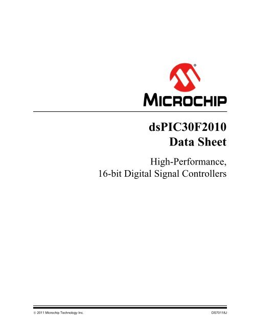
This document contains device specific information for<br />
the <strong>dsPIC30F2010</strong> device. The dsPIC30F devices<br />
contain extensive Digital Signal Processor (DSP)<br />
functionality within a high-performance 16-bit<br />
microcontroller (MCU) architecture. Figure 1-1 shows a<br />
device block diagram for the <strong>dsPIC30F2010</strong> device.<br />
© 2011 <strong>Microchip</strong> Technology Inc. DS70118J-page 7
<strong>dsPIC30F2010</strong><br />
FIGURE 1-1:<br />
<strong>dsPIC30F2010</strong> BLOCK DIAGRAM<br />
Y <strong>Data</strong> Bus<br />
X <strong>Data</strong> Bus<br />
Interrupt<br />
Controller<br />
24<br />
Address Latch<br />
Program Memory<br />
(12 Kbytes)<br />
<strong>Data</strong> EEPROM<br />
(1 Kbyte)<br />
<strong>Data</strong> Latch<br />
24<br />
24<br />
PSV and Table<br />
<strong>Data</strong> Access<br />
Control Block<br />
16<br />
8<br />
16<br />
PCU PCH PCL<br />
Program Counter<br />
Stack Loop<br />
Control Control<br />
Logic Logic<br />
16<br />
16 16 16<br />
<strong>Data</strong> Latch <strong>Data</strong> Latch<br />
Y <strong>Data</strong> X <strong>Data</strong><br />
RAM RAM<br />
(256 bytes) (256 bytes)<br />
Address Address<br />
Latch Latch<br />
16 16 16<br />
Y AGU<br />
X RAGU<br />
X WAGU<br />
Effective Address<br />
16<br />
PORTB<br />
EMUD3/AN0/VREF+/CN2/RB0<br />
EMUC3/AN1/VREF-/CN3/RB1<br />
AN2/SS1/CN4/RB2<br />
AN3/INDX/CN5/RB3<br />
AN4/QEA/IC7/CN6/RB4<br />
AN5/QEB/IC8/CN7/RB5<br />
24<br />
ROM Latch<br />
16<br />
16<br />
Instruction<br />
Decode and<br />
Control<br />
IR<br />
Decode<br />
16<br />
16 x 16<br />
W Reg Array<br />
16<br />
16<br />
PORTC<br />
EMUD1/SOSCI/T2CK/U1ATX/CN1/RC13<br />
EMUC1/SOSCO/T1CK/U1ARX/CN0/RC14<br />
OSC2/CLKO/RC15<br />
Control Signals<br />
to Various Blocks<br />
OSC1/CLKI<br />
Timing<br />
Generation<br />
MCLR<br />
Power-up<br />
Timer<br />
Oscillator<br />
Start-up Timer<br />
POR/BOR<br />
Reset<br />
Watchdog<br />
Timer<br />
16<br />
DSP<br />
Engine<br />
Divide<br />
Unit<br />
ALU<br />
16<br />
PORTD<br />
EMUC2/OC1/IC1/INT1/RD0<br />
EMUD2/OC2/IC2/INT2/RD1<br />
SPI1<br />
10-bit ADC<br />
Timers<br />
Input<br />
Capture<br />
Module<br />
QEI<br />
Output<br />
Compare<br />
Module<br />
Motor Control<br />
PWM<br />
I 2 C<br />
UART1<br />
PORTE<br />
PWM1L/RE0<br />
PWM1H/RE1<br />
PWM2L/RE2<br />
PWM2H/RE3<br />
PWM3L/RE4<br />
PWM3H/RE5<br />
FLTA/INT0/SCK1/OCFA/RE8<br />
PGC/EMUC/U1RX/SDI1/SDA/RF2<br />
PGD/EMUD/U1TX/SDO1/SCL/RF3<br />
PORTF<br />
DS70118J-page 8<br />
© 2011 <strong>Microchip</strong> Technology Inc.
<strong>dsPIC30F2010</strong><br />
Table 1-1 provides a brief description of device I/O pinouts<br />
and the functions that may be multiplexed to a port<br />
pin. Multiple functions may exist on one port pin. When<br />
multiplexing occurs, the peripheral module’s functional<br />
requirements may force an override of the data<br />
direction of the port pin.<br />
TABLE 1-1: PINOUT I/O DESCRIPTIONS<br />
Pin Name<br />
Pin<br />
Type<br />
Buffer<br />
Type<br />
Description<br />
AN0-AN5 I Analog Analog input channels.<br />
AVDD P P Positive supply for analog module. This pin must be connected at all times.<br />
AVSS P P Ground reference for analog module. This pin must be connected at all times.<br />
CLKI<br />
CLKO<br />
I<br />
O<br />
ST/CMOS<br />
—<br />
External clock source input. Always associated with OSC1 pin function.<br />
Oscillator crystal output. Connects to crystal or resonator in Crystal<br />
Oscillator mode. Optionally functions as CLKO in RC and EC modes. Always<br />
associated with OSC2 pin function.<br />
CN0-CN7 I ST Input change notification inputs.<br />
Can be software programmed for internal weak pull-ups on all inputs.<br />
EMUD<br />
EMUC<br />
EMUD1<br />
EMUC1<br />
EMUD2<br />
EMUC2<br />
EMUD3<br />
EMUC3<br />
IC1, IC2, IC7,<br />
IC8<br />
INDX<br />
QEA<br />
QEB<br />
INT0<br />
INT1<br />
INT2<br />
FLTA<br />
PWM1L<br />
PWM1H<br />
PWM2L<br />
PWM2H<br />
PWM3L<br />
PWM3H<br />
I/O<br />
I/O<br />
I/O<br />
I/O<br />
I/O<br />
I/O<br />
I/O<br />
I/O<br />
ST<br />
ST<br />
ST<br />
ST<br />
ST<br />
ST<br />
ST<br />
ST<br />
ICD Primary Communication Channel data input/output pin.<br />
ICD Primary Communication Channel clock input/output pin.<br />
ICD Secondary Communication Channel data input/output pin.<br />
ICD Secondary Communication Channel clock input/output pin.<br />
ICD Tertiary Communication Channel data input/output pin.<br />
ICD Tertiary Communication Channel clock input/output pin.<br />
ICD Quaternary Communication Channel data input/output pin.<br />
ICD Quaternary Communication Channel clock input/output pin.<br />
I ST Capture inputs. The <strong>dsPIC30F2010</strong> has four capture inputs. The inputs are<br />
numbered for consistency with the inputs on larger device variants.<br />
I<br />
I<br />
I<br />
I<br />
I<br />
I<br />
I<br />
O<br />
O<br />
O<br />
O<br />
O<br />
O<br />
ST<br />
ST<br />
ST<br />
ST<br />
ST<br />
ST<br />
ST<br />
—<br />
—<br />
—<br />
—<br />
—<br />
—<br />
Quadrature Encoder Index Pulse input.<br />
Quadrature Encoder Phase A input in QEI mode.<br />
Auxiliary Timer External Clock/Gate input in Timer mode.<br />
Quadrature Encoder Phase B input in QEI mode.<br />
Auxiliary Timer External Clock/Gate input in Timer mode.<br />
External interrupt 0<br />
External interrupt 1<br />
External interrupt 2<br />
PWM Fault A input<br />
PWM 1 Low output<br />
PWM 1 High output<br />
PWM 2 Low output<br />
PWM 2 High output<br />
PWM 3 Low output<br />
PWM 3 High output<br />
MCLR I/P ST Master Clear (Reset) input or programming voltage input. This pin is an<br />
active-low Reset to the device.<br />
OCFA<br />
OC1-OC2<br />
OSC1<br />
OSC2<br />
I<br />
O<br />
I<br />
I/O<br />
ST<br />
—<br />
ST/CMOS<br />
—<br />
Compare Fault A input (for Compare channels 1, 2, 3 and 4).<br />
Compare outputs.<br />
Oscillator crystal input. ST buffer when configured in RC mode; CMOS<br />
otherwise.<br />
Oscillator crystal output. Connects to crystal or resonator in Crystal Oscillator<br />
mode. Optionally functions as CLKO in RC and EC modes.<br />
Legend: CMOS = CMOS compatible input or output Analog = Analog input<br />
ST = Schmitt Trigger input with CMOS levels O = Output<br />
I = Input P = Power<br />
© 2011 <strong>Microchip</strong> Technology Inc. DS70118J-page 9
<strong>dsPIC30F2010</strong><br />
TABLE 1-1:<br />
Pin Name<br />
PGD<br />
PGC<br />
I/O<br />
I<br />
ST<br />
ST<br />
In-Circuit Serial Programming (ICSP) data input/output pin.<br />
In-Circuit Serial Programming clock input pin.<br />
RB0-RB5 I/O ST PORTB is a bidirectional I/O port.<br />
RC13-RC14 I/O ST PORTC is a bidirectional I/O port.<br />
RD0-RD1 I/O ST PORTD is a bidirectional I/O port.<br />
RE0-RE5, I/O ST PORTE is a bidirectional I/O port.<br />
RE8<br />
RF2, RF3 I/O ST PORTF is a bidirectional I/O port.<br />
SCK1<br />
SDI1<br />
SDO1<br />
SS1<br />
SCL<br />
SDA<br />
SOSCO<br />
SOSCI<br />
T1CK<br />
T2CK<br />
U1RX<br />
U1TX<br />
U1ARX<br />
U1ATX<br />
PINOUT I/O DESCRIPTIONS (CONTINUED)<br />
Pin<br />
Type<br />
I/O<br />
I<br />
O<br />
I<br />
I/O<br />
I/O<br />
O<br />
I<br />
I<br />
I<br />
I<br />
O<br />
I<br />
O<br />
Buffer<br />
Type<br />
ST<br />
ST<br />
—<br />
ST<br />
ST<br />
ST<br />
—<br />
ST/CMOS<br />
ST<br />
ST<br />
ST<br />
—<br />
ST<br />
—<br />
Synchronous serial clock input/output for SPI1.<br />
SPI1 <strong>Data</strong> In.<br />
SPI1 <strong>Data</strong> Out.<br />
SPI1 Slave Synchronization.<br />
Synchronous serial clock input/output for I 2 C.<br />
Synchronous serial data input/output for I 2 C.<br />
32 kHz low-power oscillator crystal output.<br />
32 kHz low-power oscillator crystal input. ST buffer when configured in RC<br />
mode; CMOS otherwise.<br />
Timer1 external clock input.<br />
Timer2 external clock input.<br />
UART1 Receive.<br />
UART1 Transmit.<br />
UART1 Alternate Receive.<br />
UART1 Alternate Transmit.<br />
Description<br />
VDD P — Positive supply for logic and I/O pins.<br />
VSS P — Ground reference for logic and I/O pins.<br />
VREF+ I Analog Analog Voltage Reference (High) input.<br />
VREF- I Analog Analog Voltage Reference (Low) input.<br />
Legend: CMOS = CMOS compatible input or output Analog = Analog input<br />
ST = Schmitt Trigger input with CMOS levels O = Output<br />
I = Input P = Power<br />
DS70118J-page 10<br />
© 2011 <strong>Microchip</strong> Technology Inc.
<strong>dsPIC30F2010</strong><br />
2.0 CPU ARCHITECTURE<br />
OVERVIEW<br />
Note:<br />
This data sheet summarizes features of<br />
this group of dsPIC30F devices and is not<br />
intended to be a complete reference<br />
source. For more information on the CPU,<br />
peripherals, register descriptions and<br />
general device functionality, refer to the<br />
“dsPIC30F Family Reference Manual”<br />
(DS70046). For more information on the<br />
device instruction set and programming,<br />
refer to the “16-bit MCU and DSC Programmer’s<br />
Reference Manual”<br />
(DS70157).<br />
2.1 Core Overview<br />
The core has a 24-bit instruction word. The Program<br />
Counter (PC) is 23 bits wide with the Least Significant<br />
bit (LSb) always clear (see Section 3.1 “Program<br />
Address Space”), and the Most Significant bit (MSb)<br />
is ignored during normal program execution, except for<br />
certain specialized instructions. Thus, the PC can<br />
address up to 4M instruction words of user program<br />
space. An instruction prefetch mechanism is used to<br />
help maintain throughput. Program loop constructs,<br />
free from loop count management overhead, are supported<br />
using the DO and REPEAT instructions, both of<br />
which are interruptible at any point.<br />
The working register array consists of 16x16-bit registers,<br />
each of which can act as data, address or offset<br />
registers. One working register (W15) operates as a<br />
software Stack Pointer for interrupts and calls.<br />
The data space is 64 Kbytes (32K words) and is split<br />
into two blocks, referred to as X and Y data memory.<br />
Each block has its own independent Address Generation<br />
Unit (AGU). Most instructions operate solely<br />
through the X memory AGU, which provides the<br />
appearance of a single unified data space. The<br />
Multiply-Accumulate (MAC) class of dual source DSP<br />
instructions operate through both the X and Y AGUs,<br />
splitting the data address space into two parts (see<br />
Section 3.2 “<strong>Data</strong> Address Space”). The X and Y<br />
data space boundary is device specific and cannot be<br />
altered by the user. Each data word consists of 2 bytes,<br />
and most instructions can address data either as words<br />
or bytes.<br />
There are two methods of accessing data stored in<br />
program memory:<br />
• The upper 32 Kbytes of data space memory can be<br />
mapped into the lower half (user space) of program<br />
space at any 16K program word boundary, defined by<br />
the 8-bit Program Space Visibility Page (PSVPAG)<br />
register. This lets any instruction access program<br />
space as if it were data space, with a limitation that<br />
the access requires an additional cycle. Moreover,<br />
only the lower 16 bits of each instruction word can be<br />
accessed using this method.<br />
• Linear indirect access of 32K word pages within<br />
program space is also possible using any working<br />
register, via table read and write instructions.<br />
Table read and write instructions can be used to<br />
access all 24 bits of an instruction word.<br />
Overhead-free circular buffers (Modulo Addressing)<br />
are supported in both X and Y address spaces. This is<br />
primarily intended to remove the loop overhead for<br />
DSP algorithms.<br />
The X AGU also supports Bit-Reversed Addressing on<br />
destination effective addresses, to greatly simplify input<br />
or output data reordering for radix-2 FFT algorithms.<br />
Refer to Section 4.0 “Address Generator Units” for<br />
details on Modulo and Bit-Reversed Addressing.<br />
The core supports Inherent (no operand), Relative, Literal,<br />
Memory Direct, Register Direct, Register Indirect,<br />
Register Offset and Literal Offset Addressing modes.<br />
Instructions are associated with predefined Addressing<br />
modes, depending upon their functional requirements.<br />
For most instructions, the core is capable of executing<br />
a data (or program data) memory read, a working register<br />
(data) read, a data memory write and a program<br />
(instruction) memory read per instruction cycle. As a<br />
result, 3-operand instructions are supported, allowing<br />
C = A + B operations to be executed in a single cycle.<br />
A DSP engine has been included to significantly<br />
enhance the core arithmetic capability and throughput.<br />
It features a high-speed 17-bit by 17-bit multiplier, a<br />
40-bit ALU, two 40-bit saturating accumulators and a<br />
40-bit bidirectional barrel shifter. <strong>Data</strong> in the accumulator<br />
or any working register can be shifted up to 15 bits<br />
right or 16 bits left in a single cycle. The DSP instructions<br />
operate seamlessly with all other instructions and<br />
have been designed for optimal real-time performance.<br />
The MAC class of instructions can concurrently fetch<br />
two data operands from memory, while multiplying two<br />
W registers. To enable this concurrent fetching of data<br />
operands, the data space has been split for these<br />
instructions and linear for all others. This has been<br />
achieved in a transparent and flexible manner, by<br />
dedicating certain working registers to each address<br />
space for the MAC class of instructions.<br />
The core does not support a multi-stage instruction<br />
pipeline. However, a single stage instruction prefetch<br />
mechanism is used, which accesses and partially<br />
decodes instructions a cycle ahead of execution, in<br />
order to maximize available execution time. Most<br />
instructions execute in a single cycle, with certain<br />
exceptions.<br />
The core features a vectored exception processing<br />
structure for traps and interrupts, with 62 independent<br />
vectors. The exceptions consist of up to 8 traps (of<br />
which 4 are reserved) and 54 interrupts. Each interrupt<br />
is prioritized based on a user-assigned priority between<br />
1 and 7 (1 being the lowest priority and 7 being the<br />
highest) in conjunction with a predetermined ‘natural<br />
order’. Traps have fixed priorities, ranging from 8 to 15.<br />
© 2011 <strong>Microchip</strong> Technology Inc. DS70118J-page 11
<strong>dsPIC30F2010</strong><br />
2.2 Programmer’s Model<br />
The programmer’s model is shown in Figure 2-1 and<br />
consists of 16 x 16-bit working registers (W0 through<br />
W15), 2 x 40-bit accumulators (ACCA and ACCB),<br />
STATUS Register (SR), <strong>Data</strong> Table Page register<br />
(TBLPAG), Program Space Visibility Page register<br />
(PSVPAG), DO and REPEAT registers (DOSTART,<br />
DOEND, DCOUNT and RCOUNT) and Program Counter<br />
(PC). The working registers can act as data,<br />
address or offset registers. All registers are memory<br />
mapped. W0 acts as the W register for file register<br />
addressing.<br />
Some of these registers have a shadow register associated<br />
with each of them, as shown in Figure 2-1. The<br />
shadow register is used as a temporary holding register<br />
and can transfer its contents to or from its host register<br />
upon the occurrence of an event. None of the shadow<br />
registers are accessible directly. The following rules<br />
apply for transfer of registers into and out of shadows.<br />
• PUSH.S and POP.S<br />
W0, W1, W2, W3, SR (DC, N, OV, Z and C bits<br />
only) are transferred.<br />
• DO instruction<br />
DOSTART, DOEND, DCOUNT shadows are<br />
pushed on loop start, and popped on loop end.<br />
When a byte operation is performed on a working register,<br />
only the Least Significant Byte (LSB) of the target<br />
register is affected. However, a benefit of memory<br />
mapped working registers is that both the Least and<br />
Most Significant Bytes can be manipulated through<br />
byte wide data memory space accesses.<br />
2.2.1 SOFTWARE STACK POINTER/<br />
FRAME POINTER<br />
The dsPIC ® DSC devices contain a software stack.<br />
W15 is the dedicated software Stack Pointer (SP), and<br />
will be automatically modified by exception processing<br />
and subroutine calls and returns. However, W15 can be<br />
referenced by any instruction in the same manner as all<br />
other W registers. This simplifies the reading, writing<br />
and manipulation of the Stack Pointer (e.g., creating<br />
stack frames).<br />
Note:<br />
In order to protect against misaligned<br />
stack accesses, W15 is always clear.<br />
W15 is initialized to 0x0800 during a Reset. The user<br />
may reprogram the SP during initialization to any<br />
location within data space.<br />
W14 has been dedicated as a Stack Frame Pointer as<br />
defined by the LNK and ULNK instructions. However,<br />
W14 can be referenced by any instruction in the same<br />
manner as all other W registers.<br />
2.2.2 STATUS REGISTER<br />
The dsPIC DSC core has a 16-bit STATUS Register<br />
(SR), the LSB of which is referred to as the SR Low<br />
Byte (SRL) and the MSB as the SR High Byte (SRH).<br />
See Figure 2-1 for SR layout.<br />
SRL contains all the MCU ALU operation status flags<br />
(including the Z bit), as well as the CPU Interrupt Priority<br />
Level status bits, IPL, and the REPEAT active<br />
status bit, RA. During exception processing, SRL is<br />
concatenated with the MSB of the PC to form a<br />
complete word value which is then stacked.<br />
The upper byte of the STATUS register contains the<br />
DSP adder/subtracter status bits, the DO Loop Active<br />
bit (DA) and the Digit Carry (DC) status bit.<br />
2.2.3 PROGRAM COUNTER<br />
The Program Counter is 23 bits wide. Bit 0 is always<br />
clear. Therefore, the PC can address up to 4M<br />
instruction words.<br />
DS70118J-page 12<br />
© 2011 <strong>Microchip</strong> Technology Inc.
<strong>dsPIC30F2010</strong><br />
FIGURE 2-1:<br />
PROGRAMMER’S MODEL<br />
D15<br />
D0<br />
W0/WREG<br />
W1<br />
W2<br />
PUSH.S Shadow<br />
DO Shadow<br />
W3<br />
W4<br />
Legend<br />
DSP Operand<br />
Registers<br />
W5<br />
W6<br />
W7<br />
W8<br />
Working Registers<br />
DSP Address<br />
Registers<br />
W9<br />
W10<br />
W11<br />
W12/DSP Offset<br />
W13/DSP Write-Back<br />
W14/Frame Pointer<br />
W15/Stack Pointer<br />
SPLIM<br />
Stack Pointer Limit Register<br />
AD39<br />
AD31<br />
AD15<br />
AD0<br />
DSP<br />
Accumulators<br />
ACCA<br />
ACCB<br />
PC22<br />
PC0<br />
0<br />
Program Counter<br />
7 0<br />
TBLPAG TABPAG<br />
<strong>Data</strong> Table Page Address<br />
7 0<br />
PSVPAG<br />
Program Space Visibility Page Address<br />
15 0<br />
RCOUNT<br />
15 0<br />
DCOUNT<br />
REPEAT Loop Counter<br />
DO Loop Counter<br />
22 0<br />
DOSTART<br />
DO Loop Start Address<br />
22<br />
DOEND<br />
DO Loop End Address<br />
15 0<br />
CORCON<br />
Core Configuration Register<br />
OA OB SA SB<br />
OAB SAB<br />
DA DC IPL2 IPL1 IPL0 RA N OV<br />
Z<br />
C<br />
STATUS Register<br />
SRH<br />
SRL<br />
© 2011 <strong>Microchip</strong> Technology Inc. DS70118J-page 13
<strong>dsPIC30F2010</strong><br />
2.3 Divide Support<br />
The dsPIC DSC devices feature a 16/16-bit signed<br />
fractional divide operation, as well as 32/16-bit and 16/<br />
16-bit signed and unsigned integer divide operations, in<br />
the form of single instruction iterative divides. The<br />
following instructions and data sizes are supported:<br />
• DIVF – 16/16 signed fractional divide<br />
• DIV.sd – 32/16 signed divide<br />
• DIV.ud – 32/16 unsigned divide<br />
• DIV.sw – 16/16 signed divide<br />
• DIV.uw – 16/16 unsigned divide<br />
The 16/16 divides are similar to the 32/16 (same number<br />
of iterations), but the dividend is either zero-extended or<br />
sign-extended during the first iteration.<br />
The divide instructions must be executed within a<br />
REPEAT loop. Any other form of execution (e.g., a<br />
series of discrete divide instructions) will not function<br />
correctly because the instruction flow depends on<br />
RCOUNT. The divide instruction does not automatically<br />
set up the RCOUNT value, and it must, therefore, be<br />
explicitly and correctly specified in the REPEAT instruction,<br />
as shown in Table 2-2 (REPEAT will execute the<br />
target instruction {operand value + 1} times). The<br />
REPEAT loop count must be set up for 18 iterations of<br />
the DIV/DIVF instruction. Thus, a complete divide<br />
operation requires 19 cycles.<br />
Note:<br />
The Divide flow is interruptible; however,<br />
the user needs to save the context as<br />
appropriate.<br />
2.4 DSP Engine<br />
The DSP engine consists of a high-speed 17-bit x<br />
17-bit multiplier, a barrel shifter, and a 40-bit adder/subtracter<br />
(with two target accumulators, round and<br />
saturation logic).<br />
The DSP engine also has the capability to perform inherent<br />
accumulator-to-accumulator operations, which<br />
require no additional data. These instructions are ADD,<br />
SUB, and NEG.<br />
The DSP engine has various options selected through<br />
various bits in the CPU Core Configuration Register<br />
(CORCON), as listed below:<br />
• Fractional or integer DSP multiply (IF).<br />
• Signed or unsigned DSP multiply (US).<br />
• Conventional or convergent rounding (RND).<br />
• Automatic saturation on/off for ACCA (SATA).<br />
• Automatic saturation on/off for ACCB (SATB).<br />
• Automatic saturation on/off for writes to data<br />
memory (SATDW).<br />
• Accumulator Saturation mode selection (ACC-<br />
SAT).<br />
Note: For CORCON layout, see Table 3-3.<br />
A block diagram of the DSP engine is shown in<br />
Figure 2-2.<br />
TABLE 2-1: DSP INSTRUCTION<br />
SUMMARY<br />
Instruction<br />
Algebraic<br />
Operation<br />
ACC WB?<br />
CLR A = 0 Yes<br />
ED A = (x – y) 2 No<br />
EDAC A = A + (x – y) 2 No<br />
MAC A = A + (x • y) Yes<br />
MAC A = A + x 2 No<br />
MOVSAC No change in A Yes<br />
MPY A = x • y No<br />
MPY.N A = – x • y No<br />
MSC A = A – x • y Yes<br />
TABLE 2-2: DIVIDE INSTRUCTIONS<br />
Instruction<br />
Function<br />
DIVF<br />
Signed fractional divide: Wm/Wn →W0; Rem →W1<br />
DIV.sd<br />
Signed divide: (Wm + 1:Wm)/Wn →W0; Rem →W1<br />
DIV.ud<br />
Unsigned divide: (Wm + 1:Wm)/Wn →W0; Rem →W1<br />
DIV.sw (or DIV.s)<br />
Signed divide: Wm/Wn →W0; Rem →W1<br />
DIV.uw (or DIV.u)<br />
Unsigned divide: Wm/Wn →W0; Rem →W1<br />
DS70118J-page 14<br />
© 2011 <strong>Microchip</strong> Technology Inc.
<strong>dsPIC30F2010</strong><br />
FIGURE 2-2: DSP ENGINE BLOCK DIAGRAM<br />
40 40-bit Accumulator A<br />
40-bit Accumulator B<br />
40<br />
Carry/Borrow Out<br />
Saturate<br />
Round<br />
Logic<br />
S<br />
a<br />
t<br />
u<br />
r<br />
a<br />
t<br />
e<br />
16<br />
Carry/Borrow In<br />
Adder<br />
Negate<br />
40<br />
40<br />
40<br />
Barrel<br />
Shifter<br />
16<br />
40<br />
Sign-Extend<br />
X <strong>Data</strong> Bus<br />
Y <strong>Data</strong> Bus<br />
33<br />
32<br />
32<br />
Zero Backfill<br />
16<br />
17-bit<br />
Multiplier/Scaler<br />
16 16<br />
To/From W Array<br />
© 2011 <strong>Microchip</strong> Technology Inc. DS70118J-page 15
<strong>dsPIC30F2010</strong><br />
2.4.1 MULTIPLIER<br />
The 17 x 17-bit multiplier is capable of signed or<br />
unsigned operation and can multiplex its output<br />
using a scaler to support either 1.31 fractional (Q31)<br />
or 32-bit integer results. Unsigned operands are<br />
zero-extended into the 17th bit of the multiplier input<br />
value. Signed operands are sign-extended into the<br />
17th bit of the multiplier input value. The output of<br />
the 17 x 17-bit multiplier/scaler is a 33-bit value,<br />
which is sign-extended to 40 bits. Integer data is<br />
inherently represented as a signed two’s complement<br />
value, where the MSB is defined as a sign bit.<br />
Generally speaking, the range of an N-bit two’s<br />
complement integer is -2 N-1 to 2 N-1 – 1. For a 16-bit<br />
integer, the data range is -32768 (0x8000) to 32767<br />
(0x7FFF), including ‘0’. For a 32-bit integer, the data<br />
range is -2,147,483,648 (0x8000 0000) to<br />
2,147,483,645 (0x7FFF FFFF).<br />
When the multiplier is configured for fractional<br />
multiplication, the data is represented as a two’s<br />
complement fraction, where the MSB is defined as a<br />
sign bit and the radix point is implied to lie just after the<br />
sign bit (QX format). The range of an N-bit two’s<br />
complement fraction with this implied radix point is -1.0<br />
to (1-2 1-N ). For a 16-bit fraction, the Q15 data range is<br />
-1.0 (0x8000) to 0.999969482 (0x7FFF), including ‘0’<br />
and has a precision of 3.01518x10 -5 . In Fractional<br />
mode, a 16x16 multiply operation generates a 1.31<br />
product, which has a precision of 4.65661x10 -10 .<br />
The same multiplier is used to support the MCU multiply<br />
instructions, which include integer 16-bit signed,<br />
unsigned and mixed sign multiplies.<br />
The MUL instruction may be directed to use byte or<br />
word-sized operands. Byte operands will direct a 16-bit<br />
result, and word operands will direct a 32-bit result to<br />
the specified register(s) in the W array.<br />
2.4.2 DATA ACCUMULATORS AND<br />
ADDER/SUBTRACTER<br />
The data accumulator consists of a 40-bit adder/<br />
subtracter with automatic sign extension logic. It can<br />
select one of two accumulators (A or B) as its preaccumulation<br />
source and post-accumulation<br />
destination. For the ADD and LAC instructions, the data<br />
to be accumulated or loaded can be optionally scaled<br />
via the barrel shifter, prior to accumulation.<br />
2.4.2.1 Adder/Subtracter, Overflow and<br />
Saturation<br />
The adder/subtracter is a 40-bit adder with an optional<br />
zero input into one side and either true or complement<br />
data into the other input. In the case of addition, the<br />
carry/borrow input is active high and the other input is<br />
true data (not complemented), whereas in the case of<br />
subtraction, the carry/borrow input is active low and the<br />
other input is complemented. The adder/subtracter<br />
generates overflow status bits SA/SB and OA/OB,<br />
which are latched and reflected in the STATUS<br />
Register.<br />
• Overflow from bit 39: this is a catastrophic<br />
overflow in which the sign of the accumulator is<br />
destroyed.<br />
• Overflow into guard bits 32 through 39: this is a<br />
recoverable overflow. This bit is set whenever all<br />
the guard bits are not identical to each other.<br />
The adder has an additional saturation block which<br />
controls accumulator data saturation, if selected. It<br />
uses the result of the adder, the overflow status bits<br />
described above, and the SATA/B (CORCON)<br />
and ACCSAT (CORCON) mode control bits to<br />
determine when and to what value to saturate.<br />
Six STATUS register bits have been provided to<br />
support saturation and overflow; they are:<br />
1. OA:<br />
ACCA overflowed into guard bits<br />
2. OB:<br />
ACCB overflowed into guard bits<br />
3. SA:<br />
ACCA saturated (bit 31 overflow and saturation)<br />
or<br />
ACCA overflowed into guard bits and saturated<br />
(bit 39 overflow and saturation)<br />
4. SB:<br />
ACCB saturated (bit 31 overflow and saturation)<br />
or<br />
ACCB overflowed into guard bits and saturated<br />
(bit 39 overflow and saturation)<br />
5. OAB:<br />
Logical OR of OA and OB<br />
6. SAB:<br />
Logical OR of SA and SB<br />
The OA and OB bits are modified each time data<br />
passes through the adder/subtracter. When set, they<br />
indicate that the most recent operation has overflowed<br />
into the accumulator guard bits (bits 32 through 39).<br />
The OA and OB bits can also optionally generate an<br />
arithmetic warning trap when set and the corresponding<br />
overflow trap flag enable bit (OVATE, OVBTE) in<br />
the INTCON1 register (refer to Section 5.0 “Interrupts”)<br />
is set. This allows the user to take immediate<br />
action, for example, to correct system gain.<br />
DS70118J-page 16<br />
© 2011 <strong>Microchip</strong> Technology Inc.
<strong>dsPIC30F2010</strong><br />
The SA and SB bits are modified each time data passes<br />
through the adder/subtracter, but can only be cleared by<br />
the user. When set, they indicate that the accumulator<br />
has overflowed its maximum range (bit 31 for 32-bit<br />
saturation, or bit 39 for 40-bit saturation) and will be<br />
saturated (if saturation is enabled). When saturation is<br />
not enabled, SA and SB default to bit 39 overflow and<br />
thus indicate that a catastrophic overflow has occurred.<br />
If the COVTE bit in the INTCON1 register is set, SA and<br />
SB bits will generate an arithmetic warning trap when<br />
saturation is disabled.<br />
The overflow and saturation status bits can optionally<br />
be viewed in the Status Register (SR) as the logical OR<br />
of OA and OB (in bit OAB), and the logical OR of SA<br />
and SB (in bit SAB). This allows programmers to check<br />
one bit in the STATUS register to determine if either<br />
accumulator has overflowed, or one bit to determine if<br />
either accumulator has saturated. This would be useful<br />
for complex number arithmetic which typically uses<br />
both the accumulators.<br />
The device supports three Saturation and Overflow<br />
modes.<br />
1. Bit 39 Overflow and Saturation:<br />
When bit 39 overflow and saturation occurs, the<br />
saturation logic loads the maximally positive 9.31<br />
(0x7FFFFFFFFF) or maximally negative 9.31<br />
value (0x8000000000) into the target accumulator.<br />
The SA or SB bit is set and remains set until<br />
cleared by the user. This is referred to as ‘super<br />
saturation’ and provides protection against erroneous<br />
data or unexpected algorithm problems<br />
(e.g., gain calculations).<br />
2. Bit 31 Overflow and Saturation:<br />
When bit 31 overflow and saturation occurs, the<br />
saturation logic then loads the maximally positive<br />
1.31 value (0x007FFFFFFF) or maximally negative<br />
1.31 value (0x0080000000) into the target<br />
accumulator. The SA or SB bit is set and remains<br />
set until cleared by the user. When this Saturation<br />
mode is in effect, the guard bits are not used (so<br />
the OA, OB or OAB bits are never set).<br />
3. Bit 39 Catastrophic Overflow<br />
The bit 39 overflow status bit from the adder is<br />
used to set the SA or SB bit, which remain set<br />
until cleared by the user. No saturation operation<br />
is performed and the accumulator is allowed to<br />
overflow (destroying its sign). If the COVTE bit in<br />
the INTCON1 register is set, a catastrophic<br />
overflow can initiate a trap exception.<br />
2.4.2.2 Accumulator ‘Write-Back’<br />
The MAC class of instructions (with the exception of<br />
MPY, MPY.N, ED and EDAC) can optionally write a<br />
rounded version of the high word (bits 31 through 16)<br />
of the accumulator that is not targeted by the instruction<br />
into data space memory. The write is performed across<br />
the X bus into combined X and Y address space. The<br />
following addressing modes are supported:<br />
1. W13, Register Direct:<br />
The rounded contents of the non-target<br />
accumulator are written into W13 as a 1.15<br />
fraction.<br />
2. [W13]+=2, Register Indirect with Post-Increment:<br />
The rounded contents of the non-target accumulator<br />
are written into the address pointed to by<br />
W13 as a 1.15 fraction. W13 is then<br />
incremented by 2 (for a word write).<br />
2.4.2.3 Round Logic<br />
The round logic is a combinational block, which<br />
performs a conventional (biased) or convergent<br />
(unbiased) round function during an accumulator write<br />
(store). The Round mode is determined by the state of<br />
the RND bit in the CORCON register. It generates a 16-<br />
bit, 1.15 data value which is passed to the data space<br />
write saturation logic. If rounding is not indicated by the<br />
instruction, a truncated 1.15 data value is stored and the<br />
least significant word (lsw) is simply discarded.<br />
Conventional rounding takes bit 15 of the accumulator,<br />
zero-extends it and adds it to the ACCxH word (bits 16<br />
through 31 of the accumulator). If the ACCxL word (bits<br />
0 through 15 of the accumulator) is between 0x8000<br />
and 0xFFFF (0x8000 included), ACCxH is incremented.<br />
If ACCxL is between 0x0000 and 0x7FFF,<br />
ACCxH is left unchanged. A consequence of this<br />
algorithm is that over a succession of random rounding<br />
operations, the value will tend to be biased slightly<br />
positive.<br />
Convergent (or unbiased) rounding operates in the<br />
same manner as conventional rounding, except when<br />
ACCxL equals 0x8000. If this is the case, the Least Significant<br />
bit (bit 16 of the accumulator) of ACCxH is<br />
examined. If it is ‘1’, ACCxH is incremented. If it is ‘0’,<br />
ACCxH is not modified. Assuming that bit 16 is effectively<br />
random in nature, this scheme will remove any<br />
rounding bias that may accumulate.<br />
The SAC and SAC.R instructions store either a truncated<br />
(SAC) or rounded (SAC.R) version of the contents<br />
of the target accumulator to data memory, via the X bus<br />
(subject to data saturation, see Section 2.4.2.4 “<strong>Data</strong><br />
Space Write Saturation”). Note that for the MAC class<br />
of instructions, the accumulator write-back operation<br />
will function in the same manner, addressing combined<br />
MCU (X and Y) data space though the X bus. For this<br />
class of instructions, the data is always subject to<br />
rounding.<br />
© 2011 <strong>Microchip</strong> Technology Inc. DS70118J-page 17
<strong>dsPIC30F2010</strong><br />
2.4.2.4 <strong>Data</strong> Space Write Saturation<br />
In addition to adder/subtracter saturation, writes to data<br />
space may also be saturated, but without affecting the<br />
contents of the source accumulator. The data space<br />
write saturation logic block accepts a 16-bit, 1.15<br />
fractional value from the round logic block as its input,<br />
together with overflow status from the original source<br />
(accumulator) and the 16-bit round adder. These are<br />
combined and used to select the appropriate 1.15<br />
fractional value as output to write to data space<br />
memory.<br />
If the SATDW bit in the CORCON register is set, data<br />
(after rounding or truncation) is tested for overflow and<br />
adjusted accordingly. For input data greater than<br />
0x007FFF, data written to memory is forced to the<br />
maximum positive 1.15 value, 0x7FFF. For input data<br />
less than 0xFF8000, data written to memory is forced to<br />
the maximum negative 1.15 value, 0x8000. The Most<br />
Significant bit of the source (bit 39) is used to determine<br />
the sign of the operand being tested.<br />
If the SATDW bit in the CORCON register is not set, the<br />
input data is always passed through unmodified under<br />
all conditions.<br />
2.4.3 BARREL SHIFTER<br />
The barrel shifter is capable of performing up to 15-bit<br />
arithmetic or logic right shifts, or up to 16-bit left shifts<br />
in a single cycle. The source can be either of the two<br />
DSP accumulators or the X bus (to support multi-bit<br />
shifts of register or memory data).<br />
The shifter requires a signed binary value to determine<br />
both the magnitude (number of bits) and direction of the<br />
shift operation. A positive value will shift the operand<br />
right. A negative value will shift the operand left. A<br />
value of 0 will not modify the operand.<br />
The barrel shifter is 40 bits wide, thereby obtaining a<br />
40-bit result for DSP shift operations and a 16-bit result<br />
for MCU shift operations. <strong>Data</strong> from the X bus is presented<br />
to the barrel shifter between bit positions 16 to<br />
31 for right shifts, and bit positions 0 to 15 for left shifts.<br />
DS70118J-page 18<br />
© 2011 <strong>Microchip</strong> Technology Inc.
<strong>dsPIC30F2010</strong><br />
3.0 MEMORY ORGANIZATION<br />
Note:<br />
This data sheet summarizes features of<br />
this group of dsPIC30F devices and is not<br />
intended to be a complete reference<br />
source. For more information on the CPU,<br />
peripherals, register descriptions and<br />
general device functionality, refer to the<br />
“dsPIC30F Family Reference Manual”<br />
(DS70046). For more information on the<br />
device instruction set and programming,<br />
refer to the “16-bit MCU and DSC Programmer’s<br />
Reference Manual”<br />
(DS70157).<br />
3.1 Program Address Space<br />
The program address space is 4M instruction words. It<br />
is addressable by a 24-bit value from either the 23-bit<br />
PC, table instruction Effective Address (EA), or data<br />
space EA, when program space is mapped into data<br />
space, as defined by Table 3-1. Note that the program<br />
space address is incremented by two between successive<br />
program words, in order to provide compatibility<br />
with data space addressing.<br />
User program space access is restricted to the lower<br />
4M instruction word address range (0x000000 to<br />
0x7FFFFE), for all accesses other than TBLRD/TBLWT,<br />
which use TBLPAG to determine user or configuration<br />
space access. In Table 3-1, Read/Write instructions,<br />
bit 23 allows access to the Device ID, the User ID<br />
and the Configuration bits. Otherwise, bit 23 is always<br />
clear.<br />
Note:<br />
The address map shown in Figure 3-1 is<br />
conceptual, and the actual memory configuration<br />
may vary across individual<br />
devices depending on available memory.<br />
FIGURE 3-1:<br />
User Memory<br />
Space<br />
Configuration Memory<br />
Space<br />
PROGRAM SPACE MEMORY<br />
MAP FOR <strong>dsPIC30F2010</strong><br />
Reset - GOTO Instruction<br />
Reset - Target Address<br />
Reserved<br />
Ext. Osc. Fail Trap<br />
Address Error Trap<br />
Stack Error Trap<br />
Arithmetic Warn. Trap<br />
Reserved<br />
Reserved<br />
Reserved<br />
Vector 0<br />
Vector 1<br />
Vector 52<br />
Vector 53<br />
Alternate Vector Table<br />
User Flash<br />
Program Memory<br />
(4K instructions)<br />
Reserved<br />
(Read 0’s)<br />
<strong>Data</strong> EEPROM<br />
(1 Kbyte)<br />
Reserved<br />
UNITID (32 instr.)<br />
Reserved<br />
Device Configuration<br />
Registers<br />
000000<br />
000002<br />
000004<br />
Vector Tables<br />
000014<br />
00007E<br />
000080<br />
0000FE<br />
000100<br />
001FFE<br />
002000<br />
7FFBFE<br />
7FFC00<br />
7FFFFE<br />
800000<br />
8005BE<br />
8005C0<br />
8005FE<br />
800600<br />
F7FFFE<br />
F80000<br />
F8000E<br />
F80010<br />
Reserved<br />
DEVID (2)<br />
FEFFFE<br />
FF0000<br />
FFFFFE<br />
© 2011 <strong>Microchip</strong> Technology Inc. DS70118J-page 19
<strong>dsPIC30F2010</strong><br />
TABLE 3-1:<br />
Access Type<br />
PROGRAM SPACE ADDRESS CONSTRUCTION<br />
Access<br />
Space<br />
Program Space Address<br />
<br />
Instruction Access User 0 PC 0<br />
TBLRD/TBLWT User (TBLPAG = 0) TBLPAG <strong>Data</strong> EA <br />
TBLRD/TBLWT Configuration (TBLPAG = 1) TBLPAG <strong>Data</strong> EA <br />
Program Space Visibility User 0 PSVPAG <strong>Data</strong> EA <br />
FIGURE 3-2:<br />
DATA ACCESS FROM PROGRAM SPACE ADDRESS GENERATION<br />
23 bits<br />
Using<br />
Program<br />
Counter<br />
0<br />
Program Counter<br />
0<br />
Select<br />
1<br />
EA<br />
Using<br />
Program<br />
Space<br />
Visibility<br />
0<br />
PSVPAG Reg<br />
8 bits<br />
15 bits<br />
EA<br />
Using<br />
Table<br />
Instruction<br />
1/0<br />
TBLPAG Reg<br />
8 bits<br />
16 bits<br />
User/<br />
Configuration<br />
Space<br />
Select<br />
24-bit EA<br />
Byte<br />
Select<br />
Note: Program Space Visibility cannot be used to access bits of a word in program memory.<br />
DS70118J-page 20<br />
© 2011 <strong>Microchip</strong> Technology Inc.
<strong>dsPIC30F2010</strong><br />
3.1.1 DATA ACCESS FROM PROGRAM<br />
MEMORY USING TABLE<br />
INSTRUCTIONS<br />
This architecture fetches 24-bit wide program memory.<br />
Consequently, instructions are always aligned. However,<br />
as the architecture is modified Harvard, data can<br />
also be present in program space.<br />
There are two methods by which program space can<br />
be accessed: via special table instructions, or through<br />
the remapping of a 16K word program space page into<br />
the upper half of data space (see Section 3.1.2 “<strong>Data</strong><br />
Access from Program Memory Using Program<br />
Space Visibility”). The TBLRDL and TBLWTL instructions<br />
offer a direct method of reading or writing the lsw<br />
of any address within program space, without going<br />
through data space. The TBLRDH and TBLWTH instructions<br />
are the only method whereby the upper 8 bits of a<br />
program space word can be accessed as data.<br />
The PC is incremented by two for each successive<br />
24-bit program word. This allows program memory<br />
addresses to directly map to data space addresses.<br />
Program memory can thus be regarded as two 16-bit<br />
word wide address spaces, residing side by side, each<br />
with the same address range. TBLRDL and TBLWTL<br />
access the space which contains the least significant<br />
data word, and TBLRDH and TBLWTH access the space<br />
which contains the Most Significant data Byte.<br />
Figure 3-2 shows how the EA is created for table operations<br />
and data space accesses (PSV = 1). Here,<br />
P refers to a program space word, whereas<br />
D refers to a data space word.<br />
A set of Table Instructions are provided to move byte or<br />
word-sized data to and from program space.<br />
1. TBLRDL: Table Read Low<br />
Word: Read the least significant word of the<br />
program address;<br />
P maps to D.<br />
Byte: Read one of the LSBs of the program<br />
address;<br />
P maps to the destination byte when byte<br />
select = 0;<br />
P maps to the destination byte when byte<br />
select = 1.<br />
2. TBLWTL: Table Write Low (refer to Section 6.0<br />
“Flash Program Memory” for details on Flash<br />
Programming).<br />
3. TBLRDH: Table Read High<br />
Word: Read the most significant word of the<br />
program address;<br />
P maps to D; D always<br />
be = 0.<br />
Byte: Read one of the MSBs of the program<br />
address;<br />
P maps to the destination byte when<br />
byte select = 0;<br />
The destination byte will always be = 0 when<br />
byte select = 1.<br />
4. TBLWTH: Table Write High (refer to Section 6.0<br />
“Flash Program Memory” for details on Flash<br />
Programming).<br />
FIGURE 3-3:<br />
PROGRAM DATA TABLE ACCESS (LEAST SIGNIFICANT WORD)<br />
PC Address<br />
0x000000<br />
0x000002<br />
0x000004<br />
0x000006<br />
00000000<br />
00000000<br />
00000000<br />
00000000<br />
23<br />
16<br />
8<br />
0<br />
Program Memory<br />
‘Phantom’ Byte<br />
(Read as ‘0’)<br />
TBLRDL.W<br />
TBLRDL.B (Wn = 0)<br />
TBLRDL.B (Wn = 1)<br />
© 2011 <strong>Microchip</strong> Technology Inc. DS70118J-page 21
<strong>dsPIC30F2010</strong><br />
FIGURE 3-4:<br />
PROGRAM DATA TABLE ACCESS (MOST SIGNIFICANT BYTE)<br />
TBLRDH.W<br />
PC Address<br />
0x000000<br />
0x000002<br />
0x000004<br />
0x000006<br />
00000000<br />
00000000<br />
00000000<br />
00000000<br />
23<br />
16<br />
8<br />
0<br />
TBLRDH.B (Wn = 0)<br />
Program Memory<br />
‘Phantom’ Byte<br />
(Read as ‘0’)<br />
TBLRDH.B (Wn = 1)<br />
3.1.2 DATA ACCESS FROM PROGRAM<br />
MEMORY USING PROGRAM SPACE<br />
VISIBILITY<br />
The upper 32 Kbytes of data space may optionally be<br />
mapped into any 16K word program space page. This<br />
provides transparent access of stored constant data<br />
from X data space, without the need to use special<br />
instructions (i.e., TBLRDL/H, TBLWTL/H instructions).<br />
Program space access through the data space occurs<br />
if the MSb of the data space EA is set and program<br />
space visibility is enabled, by setting the PSV bit in the<br />
Core Control register (CORCON). The functions of<br />
CORCON are discussed in Section 2.4 “DSP<br />
Engine”.<br />
<strong>Data</strong> accesses to this area add an additional cycle to<br />
the instruction being executed, since two program<br />
memory fetches are required.<br />
Note that the upper half of addressable data space is<br />
always part of the X data space. Therefore, when a<br />
DSP operation uses program space mapping to access<br />
this memory region, Y data space should typically contain<br />
state (variable) data for DSP operations, whereas<br />
X data space should typically contain coefficient<br />
(constant) data.<br />
Although each data space address, 0x8000 and higher,<br />
maps directly into a corresponding program memory<br />
address (see Figure 3-5), only the lower 16-bits of the<br />
24-bit program word are used to contain the data. The<br />
upper 8 bits should be programmed to force an illegal<br />
instruction to maintain machine robustness. Refer to<br />
the “16-bit MCU and DSC Programmer’s Reference<br />
Manual” (DS70157) for details on instruction encoding.<br />
Note that by incrementing the PC by 2 for each program<br />
memory word, the Least Significant 15 bits of<br />
data space addresses directly map to the Least Significant<br />
15 bits in the corresponding program space<br />
addresses. The remaining bits are provided by the Program<br />
Space Visibility Page register, PSVPAG, as<br />
shown in Figure 3-5.<br />
Note:<br />
PSV access is temporarily disabled during<br />
table reads/writes.<br />
For instructions that use PSV which are executed<br />
outside a REPEAT loop:<br />
• The following instructions will require one instruction<br />
cycle in addition to the specified execution<br />
time:<br />
- MAC class of instructions with data operand<br />
prefetch<br />
- MOV instructions<br />
- MOV.D instructions<br />
• All other instructions will require two instruction<br />
cycles in addition to the specified execution time<br />
of the instruction.<br />
For instructions that use PSV which are executed<br />
inside a REPEAT loop:<br />
• The following instances will require two instruction<br />
cycles in addition to the specified execution time<br />
of the instruction:<br />
- Execution in the first iteration<br />
- Execution in the last iteration<br />
- Execution prior to exiting the loop due to an<br />
interrupt<br />
- Execution upon re-entering the loop after an<br />
interrupt is serviced<br />
• Any other iteration of the REPEAT loop will allow<br />
the instruction, accessing data using PSV, to<br />
execute in a single cycle.<br />
DS70118J-page 22<br />
© 2011 <strong>Microchip</strong> Technology Inc.
<strong>dsPIC30F2010</strong><br />
FIGURE 3-5:<br />
DATA SPACE WINDOW INTO PROGRAM SPACE OPERATION<br />
<strong>Data</strong> Space<br />
0x0000<br />
Program Space<br />
0x100100<br />
15<br />
EA = 0<br />
PSVPAG (1)<br />
0x00<br />
8<br />
<strong>Data</strong><br />
Space<br />
EA<br />
16<br />
15<br />
EA = 1<br />
0x8000<br />
Address<br />
15 Concatenation 23<br />
23 15 0<br />
0x001200<br />
Upper half of <strong>Data</strong><br />
Space is mapped<br />
into Program Space<br />
0xFFFF<br />
0x001FFE<br />
BSET CORCON,#2 ; PSV bit set<br />
MOV #0x00, W0 ; Set PSVPAG register<br />
MOV W0, PSVPAG<br />
MOV 0x9200, W0 ; Access program memory location<br />
; using a data space access<br />
<strong>Data</strong> Read<br />
Note: PSVPAG is an 8-bit register, containing bits of the program space address<br />
(i.e., it defines the page in program space to which the upper half of data space is being mapped).<br />
3.2 <strong>Data</strong> Address Space<br />
The core has two data spaces. The data spaces can be<br />
considered either separate (for some DSP instructions),<br />
or as one unified linear address range (for MCU<br />
instructions). The data spaces are accessed using two<br />
Address Generation Units (AGUs) and separate data<br />
paths.<br />
3.2.1 DATA SPACE MEMORY MAP<br />
The data space memory is split into two blocks, X and<br />
Y data space. A key element of this architecture is that<br />
Y space is a subset of X space, and is fully contained<br />
within X space. In order to provide an apparent linear<br />
addressing space, X and Y spaces have contiguous<br />
addresses.<br />
When executing any instruction other than one of the<br />
MAC class of instructions, the X block consists of the<br />
256 byte data address space (including all Y<br />
addresses). When executing one of the MAC class of<br />
instructions, the X block consists of the 256 bytes data<br />
address space excluding the Y address block (for data<br />
reads only). In other words, all other instructions regard<br />
the entire data memory as one composite address<br />
space. The MAC class instructions extract the Y<br />
address space from data space and address it using<br />
EAs sourced from W10 and W11. The remaining X data<br />
space is addressed using W8 and W9. Both address<br />
spaces are concurrently accessed only with the MAC<br />
class instructions.<br />
A data space memory map is shown in Figure 3-6.<br />
© 2011 <strong>Microchip</strong> Technology Inc. DS70118J-page 23
<strong>dsPIC30F2010</strong><br />
FIGURE 3-6: DATA SPACE MEMORY MAP<br />
MSB<br />
Address<br />
16 bits<br />
LSB<br />
Address<br />
SFR Space<br />
(See Note)<br />
512 bytes<br />
SRAM Space<br />
0x0001<br />
0x07FF<br />
0x0801<br />
0x08FF<br />
0x0901<br />
MSB<br />
LSB<br />
SFR Space<br />
X <strong>Data</strong> RAM (X)<br />
256 bytes<br />
0x0000<br />
0x07FE<br />
0x0800<br />
0x08FE<br />
0x0900<br />
2560 bytes<br />
Near<br />
<strong>Data</strong><br />
Space<br />
Y <strong>Data</strong> RAM (Y)<br />
256 bytes<br />
0x09FF<br />
0x0A00<br />
(See Note)<br />
0x8001<br />
0x8000<br />
X <strong>Data</strong><br />
Unimplemented (X)<br />
Optionally<br />
Mapped<br />
into Program<br />
Memory<br />
0xFFFF<br />
0xFFFE<br />
Note: Unimplemented SFR or SRAM locations read as ‘0’.<br />
DS70118J-page 24<br />
© 2011 <strong>Microchip</strong> Technology Inc.
<strong>dsPIC30F2010</strong><br />
FIGURE 3-7:<br />
DATA SPACE FOR MCU AND DSP (MAC CLASS) INSTRUCTIONS<br />
SFR Space<br />
SFR Space<br />
Unused<br />
X Space<br />
(Y Space)<br />
X Space<br />
Y Space<br />
Unused<br />
Unused<br />
X Space<br />
Non-MAC Class Ops (Read/Write)<br />
MAC Class Ops (Write)<br />
MAC Class Ops Read-Only<br />
Indirect EA using any W Indirect EA using W8, W9 Indirect EA using W10, W11<br />
© 2011 <strong>Microchip</strong> Technology Inc. DS70118J-page 25
<strong>dsPIC30F2010</strong><br />
3.2.2 DATA SPACES<br />
The X data space is used by all instructions and supports<br />
all addressing modes. There are separate read<br />
and write data buses. The X read data bus is the return<br />
data path for all instructions that view data space as<br />
combined X and Y address space. It is also the X<br />
address space data path for the dual operand read<br />
instructions (MAC class). The X write data bus is the<br />
only write path to data space for all instructions.<br />
The X data space also supports Modulo Addressing for<br />
all instructions, subject to addressing mode restrictions.<br />
Bit-Reversed addressing is only supported for<br />
writes to X data space.<br />
The Y data space is used in concert with the X data<br />
space by the MAC class of instructions (CLR, ED, EDAC,<br />
MAC, MOVSAC, MPY, MPY.N and MSC) to provide two<br />
concurrent data read paths. No writes occur across the<br />
Y bus. This class of instructions dedicates two W register<br />
pointers, W10 and W11, to always address Y data<br />
space, independent of X data space, whereas W8 and<br />
W9 always address X data space. Note that during<br />
accumulator write-back, the data address space is considered<br />
a combination of X and Y data spaces, so the<br />
write occurs across the X bus. Consequently, the write<br />
can be to any address in the entire data space.<br />
The Y data space can only be used for the data<br />
prefetch operation associated with the MAC class of<br />
instructions. It also supports Modulo Addressing for<br />
automated circular buffers. Of course, all other instructions<br />
can access the Y data address space through the<br />
X data path, as part of the composite linear space.<br />
The boundary between the X and Y data spaces is<br />
defined as shown in Figure 3-6 and is not user programmable.<br />
Should an EA point to data outside its own<br />
assigned address space, or to a location outside physical<br />
memory, an all-zero word/byte will be returned. For<br />
example, although Y address space is visible by all<br />
non-MAC instructions using any Addressing mode, an<br />
attempt by a MAC instruction to fetch data from that<br />
space, using W8 or W9 (X space pointers), will return<br />
0x0000.<br />
TABLE 3-2:<br />
EFFECT OF INVALID<br />
MEMORY ACCESSES<br />
Attempted Operation<br />
EA = an unimplemented address<br />
W8 or W9 used to access Y data<br />
space in a MAC instruction<br />
W10 or W11 used to access X<br />
data space in a MAC instruction<br />
<strong>Data</strong> Returned<br />
0x0000<br />
0x0000<br />
0x0000<br />
3.2.3 DATA SPACE WIDTH<br />
The core data width is 16 bits. All internal registers are<br />
organized as 16-bit wide words. <strong>Data</strong> space memory is<br />
organized in byte addressable, 16-bit wide blocks.<br />
3.2.4 DATA ALIGNMENT<br />
To help maintain backward compatibility with PIC ®<br />
MCU devices and improve data space memory usage<br />
efficiency, the dsPIC30F instruction set supports both<br />
word and byte operations. <strong>Data</strong> is aligned in data memory<br />
and registers as words, but all data space EAs<br />
resolve to bytes. <strong>Data</strong> byte reads will read the complete<br />
word, which contains the byte, using the LSb of any EA<br />
to determine which byte to select. The selected byte is<br />
placed onto the LSB of the X data path (no byte<br />
accesses are possible from the Y data path as the MAC<br />
class of instruction can only fetch words). That is, data<br />
memory and registers are organized as two parallel<br />
byte wide entities with shared (word) address decode,<br />
but separate write lines. <strong>Data</strong> byte writes only write to<br />
the corresponding side of the array or register which<br />
matches the byte address.<br />
As a consequence of this byte accessibility, all effective<br />
address calculations (including those generated<br />
by the DSP operations, which are restricted to wordsized<br />
data) are internally scaled to step through<br />
word-aligned memory. For example, the core would<br />
recognize that Post-Modified Register Indirect<br />
Addressing mode, [Ws ++], will result in a value of<br />
Ws + 1 for byte operations and Ws + 2 for word<br />
operations.<br />
All word accesses must be aligned to an even address.<br />
Misaligned word data fetches are not supported, so<br />
care must be taken when mixing byte and word operations,<br />
or translating from 8-bit MCU code. Should a misaligned<br />
read or write be attempted, an address error<br />
trap will be generated. If the error occurred on a read,<br />
the instruction underway is completed, whereas if it<br />
occurred on a write, the instruction will be executed but<br />
the write will not occur. In either case, a trap will then<br />
be executed, allowing the system and/or user to examine<br />
the machine state prior to execution of the address<br />
fault.<br />
FIGURE 3-8:<br />
0003<br />
0005<br />
DATA ALIGNMENT<br />
MSB<br />
LSB<br />
15 8 7 0<br />
0001 Byte 1 Byte 0 0000<br />
Byte 3 Byte 2<br />
Byte 5 Byte 4<br />
0002<br />
0004<br />
All effective addresses are 16 bits wide and point to<br />
bytes within the data space. Therefore, the data space<br />
address range is 64 Kbytes or 32K words.<br />
DS70118J-page 26<br />
© 2011 <strong>Microchip</strong> Technology Inc.
<strong>dsPIC30F2010</strong><br />
All byte loads into any W register are loaded into the<br />
LSB. The MSB is not modified.<br />
A sign-extend (SE) instruction is provided to allow<br />
users to translate 8-bit signed data to 16-bit signed<br />
values. Alternatively, for 16-bit unsigned data, users<br />
can clear the MSB of any W register by executing a<br />
zero-extend (ZE) instruction on the appropriate<br />
address.<br />
Although most instructions are capable of operating on<br />
word or byte data sizes, it should be noted that some<br />
instructions, including the DSP instructions, operate<br />
only on words.<br />
3.2.5 NEAR DATA SPACE<br />
An 8 Kbyte ‘near’ data space is reserved in X address<br />
memory space between 0x0000 and 0x1FFF, which is<br />
directly addressable via a 13-bit absolute address field<br />
within all memory direct instructions. The remaining X<br />
address space and all of the Y address space is<br />
addressable indirectly. Additionally, the whole of X data<br />
space is addressable using MOV instructions, which<br />
support memory direct addressing with a 16-bit<br />
address field.<br />
There is a Stack Pointer Limit register (SPLIM) associated<br />
with the Stack Pointer. SPLIM is uninitialized at<br />
Reset. As is the case for the Stack Pointer, SPLIM<br />
is forced to ‘0’, because all stack operations must be<br />
word-aligned. Whenever an EA is generated using<br />
W15 as a source or destination pointer, the address<br />
thus generated is compared with the value in SPLIM. If<br />
the contents of the Stack Pointer (W15) and the SPLIM<br />
register are equal and a push operation is performed, a<br />
stack error trap will not occur. The stack error trap will<br />
occur on a subsequent push operation. Thus, for example,<br />
if it is desirable to cause a stack error trap when the<br />
stack grows beyond address 0x2000 in RAM, initialize<br />
the SPLIM with the value, 0x1FFE.<br />
Similarly, a stack pointer underflow (stack error) trap is<br />
generated when the Stack Pointer address is found to<br />
be less than 0x0800, thus preventing the stack from<br />
interfering with the Special Function Register (SFR)<br />
space.<br />
A write to the SPLIM register should not be immediately<br />
followed by an indirect read operation using W15.<br />
FIGURE 3-9:<br />
CALL STACK FRAME<br />
3.2.6 SOFTWARE STACK<br />
0x0000<br />
15<br />
0<br />
The dsPIC DSC device contains a software stack. W15<br />
is used as the Stack Pointer.<br />
The Stack Pointer always points to the first available<br />
free word, and grows from lower addresses towards<br />
higher addresses. It pre-decrements for stack pops,<br />
and post-increments for stack pushes, as shown in<br />
Figure 3-9. Note that for a PC push during any CALL<br />
instruction, the MSB of the PC is zero-extended before<br />
the push, ensuring that the MSB is always clear.<br />
Note:<br />
A PC push during exception processing<br />
will concatenate the SRL register to the<br />
MSB of the PC prior to the push.<br />
Stack Grows Towards<br />
Higher Address<br />
PC<br />
000000000 PC<br />
<br />
W15 (before CALL)<br />
W15 (after CALL)<br />
POP: [--W15]<br />
PUSH: [W15++]<br />
© 2011 <strong>Microchip</strong> Technology Inc. DS70118J-page 27
DS70118J-page 28 © 2011 <strong>Microchip</strong> Technology Inc.<br />
TABLE 3-3:<br />
CORE REGISTER MAP<br />
SFR Name<br />
Address<br />
(Home)<br />
Bit 15 Bit 14 Bit 13 Bit 12 Bit 11 Bit 10 Bit 9 Bit 8 Bit 7 Bit 6 Bit 5 Bit 4 Bit 3 Bit 2 Bit 1 Bit 0 Reset State<br />
W0 0000 W0 / WREG 0000 0000 0000 0000<br />
W1 0002 W1 0000 0000 0000 0000<br />
W2 0004 W2 0000 0000 0000 0000<br />
W3 0006 W3 0000 0000 0000 0000<br />
W4 0008 W4 0000 0000 0000 0000<br />
W5 000A W5 0000 0000 0000 0000<br />
W6 000C W6 0000 0000 0000 0000<br />
W7 000E W7 0000 0000 0000 0000<br />
W8 0010 W8 0000 0000 0000 0000<br />
W9 0012 W9 0000 0000 0000 0000<br />
W10 0014 W10 0000 0000 0000 0000<br />
W11 0016 W11 0000 0000 0000 0000<br />
W12 0018 W12 0000 0000 0000 0000<br />
W13 001A W13 0000 0000 0000 0000<br />
W14 001C W14 0000 0000 0000 0000<br />
W15 001E W15 0000 1000 0000 0000<br />
SPLIM 0020 SPLIM 0000 0000 0000 0000<br />
ACCAL 0022 ACCAL 0000 0000 0000 0000<br />
ACCAH 0024 ACCAH 0000 0000 0000 0000<br />
ACCAU 0026 Sign Extension (ACCA) ACCAU 0000 0000 0000 0000<br />
ACCBL 0028 ACCBL 0000 0000 0000 0000<br />
ACCBH 002A ACCBH 0000 0000 0000 0000<br />
ACCBU 002C Sign Extension (ACCB) ACCBU 0000 0000 0000 0000<br />
PCL 002E PCL 0000 0000 0000 0000<br />
PCH 0030 — — — — — — — — — PCH 0000 0000 0000 0000<br />
TBLPAG 0032 — — — — — — — — TBLPAG 0000 0000 0000 0000<br />
PSVPAG 0034 — — — — — — — — PSVPAG 0000 0000 0000 0000<br />
RCOUNT 0036 RCOUNT uuuu uuuu uuuu uuuu<br />
DCOUNT 0038 DCOUNT uuuu uuuu uuuu uuuu<br />
DOSTARTL 003A DOSTARTL 0 uuuu uuuu uuuu uuu0<br />
DOSTARTH 003C — — — — — — — — — DOSTARTH 0000 0000 0uuu uuuu<br />
DOENDL 003E DOENDL 0 uuuu uuuu uuuu uuu0<br />
DOENDH 0040 — — — — — — — — — DOENDH 0000 0000 0uuu uuuu<br />
SR 0042 OA OB SA SB OAB SAB DA DC IPL2 IPL1 IPL0 RA N OV Z C 0000 0000 0000 0000<br />
Legend: u = uninitialized bit; — = unimplemented bit, read as ‘0’<br />
Note: Refer to the “dsPIC30F Family Reference Manual” (DS70046) for descriptions of register bit fields.<br />
<strong>dsPIC30F2010</strong>
© 2011 <strong>Microchip</strong> Technology Inc. DS70118J-page 29<br />
TABLE 3-3:<br />
SFR Name<br />
Address<br />
(Home)<br />
CORE REGISTER MAP (CONTINUED)<br />
Bit 15 Bit 14 Bit 13 Bit 12 Bit 11 Bit 10 Bit 9 Bit 8 Bit 7 Bit 6 Bit 5 Bit 4 Bit 3 Bit 2 Bit 1 Bit 0 Reset State<br />
CORCON 0044 — — — US EDT DL2 DL1 DL0 SATA SATB SATDW ACCSAT IPL3 PSV RND IF 0000 0000 0010 0000<br />
MODCON 0046 XMODEN YMODEN — — BWM YWM XWM 0000 0000 0000 0000<br />
XMODSRT 0048 XS 0 uuuu uuuu uuuu uuu0<br />
XMODEND 004A XE 1 uuuu uuuu uuuu uuu1<br />
YMODSRT 004C YS 0 uuuu uuuu uuuu uuu0<br />
YMODEND 004E YE 1 uuuu uuuu uuuu uuu1<br />
XBREV 0050 BREN XB uuuu uuuu uuuu uuuu<br />
DISICNT 0052 — — DISICNT 0000 0000 0000 0000<br />
Legend: u = uninitialized bit; — = unimplemented bit, read as ‘0’<br />
Note: Refer to the “dsPIC30F Family Reference Manual” (DS70046) for descriptions of register bit fields.<br />
<strong>dsPIC30F2010</strong>
<strong>dsPIC30F2010</strong><br />
NOTES:<br />
DS70118J-page 30<br />
© 2011 <strong>Microchip</strong> Technology Inc.
<strong>dsPIC30F2010</strong><br />
4.0 ADDRESS GENERATOR UNITS<br />
Note:<br />
This data sheet summarizes features of<br />
this group of dsPIC30F devices and is not<br />
intended to be a complete reference<br />
source. For more information on the CPU,<br />
peripherals, register descriptions and<br />
general device functionality, refer to the<br />
“dsPIC30F Family Reference Manual”<br />
(DS70046). For more information on the<br />
device instruction set and programming,<br />
refer to the “16-bit MCU and DSC Programmer’s<br />
Reference Manual”<br />
(DS70157).<br />
The dsPIC DSC core contains two independent<br />
address generator units: the X AGU and Y AGU. The Y<br />
AGU supports word-sized data reads for the DSP MAC<br />
class of instructions only. The dsPIC DSC AGUs<br />
support three types of data addressing:<br />
• Linear Addressing<br />
• Modulo (Circular) Addressing<br />
• Bit-Reversed Addressing<br />
Linear and Modulo <strong>Data</strong> Addressing modes can be<br />
applied to data space or program space. Bit-Reversed<br />
Addressing is only applicable to data space addresses.<br />
4.1 Instruction Addressing Modes<br />
The Addressing modes in Table 4-1 form the basis of<br />
the Addressing modes optimized to support the specific<br />
features of individual instructions. The Addressing<br />
modes provided in the MAC class of instructions are<br />
somewhat different from those in the other instruction<br />
types.<br />
4.1.1 FILE REGISTER INSTRUCTIONS<br />
Most file register instructions use a 13-bit address field<br />
(f) to directly address data present in the first 8192<br />
bytes of data memory (near data space). Most file<br />
register instructions employ a working register W0,<br />
which is denoted as WREG in these instructions. The<br />
destination is typically either the same file register, or<br />
WREG (with the exception of the MUL instruction),<br />
which writes the result to a register or register pair. The<br />
MOV instruction allows additional flexibility and can<br />
access the entire data space.<br />
TABLE 4-1: FUNDAMENTAL ADDRESSING MODES SUPPORTED<br />
Addressing Mode<br />
Description<br />
File Register Direct<br />
Register Direct<br />
Register Indirect<br />
Register Indirect Post-modified<br />
Register Indirect Pre-modified<br />
Register Indirect with Register Offset<br />
Register Indirect with Literal Offset<br />
The address of the file register is specified explicitly.<br />
The contents of a register are accessed directly.<br />
The contents of Wn forms the Effective Address (EA).<br />
The contents of Wn forms the EA. Wn is post-modified (incremented or<br />
decremented) by a constant value.<br />
Wn is pre-modified (incremented or decremented) by a signed constant<br />
value to form the EA.<br />
The sum of Wn and Wb forms the EA.<br />
The sum of Wn and a literal forms the EA.<br />
© 2011 <strong>Microchip</strong> Technology Inc. DS70118J-page 31
<strong>dsPIC30F2010</strong><br />
4.1.2 MCU INSTRUCTIONS<br />
The three-operand MCU instructions are of the form:<br />
Operand 3 = Operand 1 Operand 2<br />
where Operand 1 is always a working register (i.e., the<br />
Addressing mode can only be register direct), which is<br />
referred to as Wb. Operand 2 can be a W register,<br />
fetched from data memory, or 5-bit literal. The result<br />
location can be either a W register or an address<br />
location. The following Addressing modes are<br />
supported by MCU instructions:<br />
• Register Direct<br />
• Register Indirect<br />
• Register Indirect Post-modified<br />
• Register Indirect Pre-modified<br />
• 5-bit or 10-bit Literal<br />
Note: Not all instructions support all the<br />
Addressing modes given above. Individual<br />
instructions may support different<br />
subsets of these Addressing modes.<br />
4.1.3 MOVE AND ACCUMULATOR<br />
INSTRUCTIONS<br />
Move instructions and the DSP Accumulator class of<br />
instructions provide a greater degree of addressing<br />
flexibility than other instructions. In addition to the<br />
Addressing modes supported by most MCU instructions,<br />
Move and Accumulator instructions also support<br />
Register Indirect with Register Offset Addressing<br />
mode, also referred to as Register Indexed mode.<br />
Note:<br />
For the MOV instructions, the Addressing<br />
mode specified in the instruction can differ<br />
for the source and destination EA. However,<br />
the 4-bit Wb (Register Offset) field is<br />
shared between both source and<br />
destination (but typically only used by<br />
one).<br />
In summary, the following Addressing modes are<br />
supported by Move and Accumulator instructions:<br />
• Register Direct<br />
• Register Indirect<br />
• Register Indirect Post-modified<br />
• Register Indirect Pre-modified<br />
• Register Indirect with Register Offset (Indexed)<br />
• Register Indirect with Literal Offset<br />
• 8-bit Literal<br />
• 16-bit Literal<br />
Note: Not all instructions support all the<br />
Addressing modes given above. Individual<br />
instructions may support different<br />
subsets of these Addressing modes.<br />
4.1.4 MAC INSTRUCTIONS<br />
The dual source operand DSP instructions (CLR, ED,<br />
EDAC, MAC, MPY, MPY.N, MOVSAC and MSC), also<br />
referred to as MAC instructions, utilize a simplified set of<br />
Addressing modes to allow the user to effectively<br />
manipulate the data pointers through register indirect<br />
tables.<br />
The two source operand prefetch registers must be a<br />
member of the set {W8, W9, W10, W11}. For data<br />
reads, W8 and W9 will always be directed to the X<br />
RAGU and W10 and W11 will always be directed to the<br />
Y AGU. The effective addresses generated (before and<br />
after modification) must, therefore, be valid addresses<br />
within X data space for W8 and W9 and Y data space<br />
for W10 and W11.<br />
Note:<br />
Register Indirect with Register Offset<br />
Addressing is only available for W9 (in X<br />
space) and W11 (in Y space).<br />
In summary, the following Addressing modes are<br />
supported by the MAC class of instructions:<br />
• Register Indirect<br />
• Register Indirect Post-modified by 2<br />
• Register Indirect Post-modified by 4<br />
• Register Indirect Post-modified by 6<br />
• Register Indirect with Register Offset (Indexed)<br />
4.1.5 OTHER INSTRUCTIONS<br />
Besides the various Addressing modes outlined above,<br />
some instructions use literal constants of various sizes.<br />
For example, BRA (branch) instructions use 16-bit<br />
signed literals to specify the branch destination directly,<br />
whereas the DISI instruction uses a 14-bit unsigned<br />
literal field. In some instructions, such as ADD Acc, the<br />
source of an operand or result is implied by the opcode<br />
itself. Certain operations, such as NOP, do not have any<br />
operands.<br />
DS70118J-page 32<br />
© 2011 <strong>Microchip</strong> Technology Inc.
<strong>dsPIC30F2010</strong><br />
4.2 Modulo Addressing<br />
Modulo addressing is a method of providing an automated<br />
means to support circular data buffers using<br />
hardware. The objective is to remove the need for software<br />
to perform data address boundary checks when<br />
executing tightly looped code, as is typical in many<br />
DSP algorithms.<br />
Modulo addressing can operate in either data or<br />
program space (since the data pointer mechanism is<br />
essentially the same for both). One circular buffer can<br />
be supported in each of the X (which also provides the<br />
pointers into Program space) and Y data spaces.<br />
Modulo addressing can operate on any W register<br />
pointer. However, it is not advisable to use W14 or W15<br />
for Modulo Addressing, since these two registers are<br />
used as the Stack Frame Pointer and Stack Pointer,<br />
respectively.<br />
In general, any particular circular buffer can only be<br />
configured to operate in one direction, as there are<br />
certain restrictions on the buffer start address (for<br />
incrementing buffers) or end address (for decrementing<br />
buffers) based upon the direction of the buffer.<br />
The only exception to the usage restrictions is for<br />
buffers which have a power-of-2 length. As these<br />
buffers satisfy the start and end address criteria, they<br />
may operate in a Bidirectional mode, (i.e., address<br />
boundary checks will be performed on both the lower<br />
and upper address boundaries).<br />
4.2.1 START AND END ADDRESS<br />
The Modulo Addressing scheme requires that a<br />
starting and an end address be specified and loaded<br />
into the 16-bit modulo buffer address registers:<br />
XMODSRT, XMODEND, YMODSRT and YMODEND<br />
(see Table 3-3).<br />
Note:<br />
Y space Modulo Addressing EA calculations<br />
assume word-sized data (LSb of<br />
every EA is always clear).<br />
The length of a circular buffer is not directly specified. It<br />
is determined by the difference between the corresponding<br />
start and end addresses. The maximum<br />
possible length of the circular buffer is 32K words<br />
(64 Kbytes).<br />
4.2.2 W ADDRESS REGISTER<br />
SELECTION<br />
The Modulo and Bit-Reversed Addressing Control register<br />
MODCON contains enable flags as well as<br />
a W register field to specify the W address registers.<br />
The XWM and YWM fields select which registers will<br />
operate with Modulo Addressing. If XWM = 15, X<br />
RAGU and X WAGU Modulo Addressing are disabled.<br />
Similarly, if YWM = 15, Y AGU Modulo Addressing is<br />
disabled.<br />
The X Address Space Pointer W register (XWM) to<br />
which Modulo Addressing is to be applied, is stored in<br />
MODCON (see Table 3-3). Modulo addressing is<br />
enabled for X data space when XWM is set to any value<br />
other than 15 and the XMODEN bit is set at<br />
MODCON.<br />
The Y Address Space Pointer W register (YWM) to<br />
which Modulo Addressing is to be applied, is stored in<br />
MODCON. Modulo addressing is enabled for Y<br />
data space when YWM is set to any value other than 15<br />
and the YMODEN bit is set at MODCON.<br />
© 2011 <strong>Microchip</strong> Technology Inc. DS70118J-page 33
<strong>dsPIC30F2010</strong><br />
FIGURE 4-1:<br />
MODULO ADDRESSING OPERATION EXAMPLE<br />
Byte<br />
Address MOV #0x1100,W0<br />
MOV W0, XMODSRT ;set modulo start address<br />
MOV #0x1163,W0<br />
MOV W0,MODEND ;set modulo end address<br />
0x1100<br />
MOV #0x8001,W0<br />
MOV W0,MODCON ;enable W1, X AGU for modulo<br />
MOV #0x0000,W0 ;W0 holds buffer fill value<br />
MOV #0x1110,W1 ;point W1 to buffer<br />
DO AGAIN,#0x31 ;fill the 50 buffer locations<br />
MOV W0, [W1++] ;fill the next location<br />
AGAIN: INC W0,W0 ;increment the fill value<br />
0x1163<br />
Start Addr = 0x1100<br />
End Addr = 0x1163<br />
Length = 0x0032 words<br />
DS70118J-page 34<br />
© 2011 <strong>Microchip</strong> Technology Inc.
<strong>dsPIC30F2010</strong><br />
4.2.3 MODULO ADDRESSING<br />
APPLICABILITY<br />
Modulo addressing can be applied to the effective<br />
address calculation associated with any W register. It is<br />
important to realize that the address boundaries check<br />
for addresses less than or greater than the upper (for<br />
incrementing buffers) and lower (for decrementing buffers)<br />
boundary addresses (not just equal to). Address<br />
changes may, therefore, jump beyond boundaries and<br />
still be adjusted correctly.<br />
Note:<br />
The modulo corrected effective address is<br />
written back to the register only when Pre-<br />
Modify or Post-Modify Addressing mode is<br />
used to compute the effective address.<br />
When an address offset (e.g., [W7 + W2])<br />
is used, modulo address correction is performed,<br />
but the contents of the register<br />
remains unchanged.<br />
4.3 Bit-Reversed Addressing<br />
Bit-Reversed Addressing is intended to simplify data<br />
reordering for radix-2 FFT algorithms. It is supported by<br />
the X AGU for data writes only.<br />
The modifier, which may be a constant value or register<br />
contents, is regarded as having its bit order reversed.<br />
The address source and destination are kept in normal<br />
order. Thus, the only operand requiring reversal is the<br />
modifier.<br />
4.3.1 BIT-REVERSED ADDRESSING<br />
IMPLEMENTATION<br />
Bit-Reversed Addressing is enabled when:<br />
1. BWM (W register selection) in the MODCON<br />
register is any value other than 15 (the stack can<br />
not be accessed using Bit-Reversed<br />
Addressing) and<br />
2. the BREN bit is set in the XBREV register and<br />
3. the Addressing mode used is Register Indirect<br />
with Pre-Increment or Post-Increment.<br />
If the length of a bit-reversed buffer is M = 2 N bytes,<br />
then the last ‘N’ bits of the data buffer start address<br />
must be zeros.<br />
XB is the bit-reversed address modifier or ‘pivot<br />
point’ which is typically a constant. In the case of an<br />
FFT computation, its value is equal to half of the FFT<br />
data buffer size.<br />
Note:<br />
When enabled, Bit-Reversed Addressing will only be<br />
executed for register indirect with pre-increment or<br />
post-increment addressing and word-sized data writes.<br />
It will not function for any other addressing mode or for<br />
byte-sized data, and normal addresses will be generated<br />
instead. When Bit-Reversed Addressing is active,<br />
the W Address Pointer will always be added to the<br />
address modifier (XB) and the offset associated with<br />
the register Indirect Addressing mode will be ignored.<br />
In addition, as word-sized data is a requirement, the<br />
LSb of the EA is ignored (and always clear).<br />
Note:<br />
All Bit-Reversed EA calculations assume<br />
word-sized data (LSb of every EA is<br />
always clear). The XB value is scaled<br />
accordingly to generate compatible (byte)<br />
addresses.<br />
Modulo addressing and Bit-Reversed<br />
Addressing should not be enabled<br />
together. In the event that the user<br />
attempts to do this, bit reversed addressing<br />
will assume priority when active for the<br />
X WAGU, and X WAGU Modulo Addressing<br />
will be disabled. However, Modulo<br />
Addressing will continue to function in the<br />
X RAGU.<br />
If Bit-Reversed Addressing has already been enabled<br />
by setting the BREN (XBREV) bit, then a write to<br />
the XBREV register should not be immediately followed<br />
by an indirect read operation using the W register that<br />
has been designated as the bit-reversed pointer.<br />
FIGURE 4-2:<br />
b15 b14 b13 b12<br />
BIT-REVERSED ADDRESS EXAMPLE<br />
b11 b10 b9 b8<br />
b7 b6 b5 b4<br />
Sequential Address<br />
b3 b2 b1 0<br />
Bit Locations Swapped Left-to-Right<br />
Around Center of Binary Value<br />
b15 b14 b13 b12<br />
b11 b10 b9 b8<br />
b7 b6 b5 b1<br />
b2 b3 b4 0<br />
Bit-Reversed Address<br />
Pivot Point<br />
XB = 0x0008 for a 16-word Bit-Reversed Buffer<br />
© 2011 <strong>Microchip</strong> Technology Inc. DS70118J-page 35
<strong>dsPIC30F2010</strong><br />
TABLE 4-2:<br />
TABLE 4-3:<br />
BIT-REVERSED ADDRESS SEQUENCE (16-ENTRY)<br />
Normal<br />
Address<br />
Bit-Reversed<br />
Address<br />
A3 A2 A1 A0 Decimal A3 A2 A1 A0 Decimal<br />
0 0 0 0 0 0 0 0 0 0<br />
0 0 0 1 1 1 0 0 0 8<br />
0 0 1 0 2 0 1 0 0 4<br />
0 0 1 1 3 1 1 0 0 12<br />
0 1 0 0 4 0 0 1 0 2<br />
0 1 0 1 5 1 0 1 0 10<br />
0 1 1 0 6 0 1 1 0 6<br />
0 1 1 1 7 1 1 1 0 14<br />
1 0 0 0 8 0 0 0 1 1<br />
1 0 0 1 9 1 0 0 1 9<br />
1 0 1 0 10 0 1 0 1 5<br />
1 0 1 1 11 1 1 0 1 13<br />
1 1 0 0 12 0 0 1 1 3<br />
1 1 0 1 13 1 0 1 1 11<br />
1 1 1 0 14 0 1 1 1 7<br />
1 1 1 1 15 1 1 1 1 15<br />
Note 1:<br />
BIT-REVERSED ADDRESS MODIFIER VALUES FOR XBREV REGISTER<br />
Buffer Size (Words) XB Bit-Reversed Address Modifier Value (1)<br />
32768 0x4000<br />
16384 0x2000<br />
8192 0x1000<br />
4096 0x0800<br />
2048 0x0400<br />
1024 0x0200<br />
512 0x0100<br />
256 0x0080<br />
128 0x0040<br />
64 0x0020<br />
32 0x0010<br />
16 0x0008<br />
8 0x0004<br />
4 0x0002<br />
2 0x0001<br />
Modifier values greater than 256 words exceed the data memory available on the <strong>dsPIC30F2010</strong> device.<br />
DS70118J-page 36<br />
© 2011 <strong>Microchip</strong> Technology Inc.
<strong>dsPIC30F2010</strong><br />
5.0 INTERRUPTS<br />
Note:<br />
This data sheet summarizes features of<br />
this group of dsPIC30F devices and is not<br />
intended to be a complete reference<br />
source. For more information on the CPU,<br />
peripherals, register descriptions and<br />
general device functionality, refer to the<br />
“dsPIC30F Family Reference Manual”<br />
(DS70046). For more information on the<br />
device instruction set and programming,<br />
refer to the “16-bit MCU and DSC Programmer’s<br />
Reference Manual”<br />
(DS70157).<br />
The <strong>dsPIC30F2010</strong> has 24 interrupt sources and four<br />
processor exceptions (traps), which must be arbitrated<br />
based on a priority scheme.<br />
The CPU is responsible for reading the Interrupt Vector<br />
Table (IVT) and transferring the address contained<br />
in the interrupt vector to the program counter. The<br />
interrupt vector is transferred from the program data<br />
bus into the program counter, via a 24-bit wide<br />
multiplexer on the input of the program counter.<br />
The Interrupt Vector Table (IVT) and Alternate Interrupt<br />
Vector Table (AIVT) are placed near the beginning<br />
of program memory (0x000004). The IVT and AIVT<br />
are shown in Figure 5-1.<br />
The interrupt controller is responsible for preprocessing<br />
the interrupts and processor exceptions,<br />
prior to their being presented to the processor core.<br />
The peripheral interrupts and traps are enabled, prioritized<br />
and controlled using centralized special function<br />
registers:<br />
• IFS0, IFS1, IFS2<br />
All interrupt request flags are maintained in these<br />
three registers. The flags are set by their respective<br />
peripherals or external signals, and they are cleared<br />
via software.<br />
• IEC0, IEC1, IEC2<br />
All interrupt enable control bits are maintained in<br />
these three registers. These control bits are used to<br />
individually enable interrupts from the peripherals or<br />
external signals.<br />
• IPC0... IPC11<br />
The user-assignable priority level associated with<br />
each of these interrupts is held centrally in these<br />
twelve registers.<br />
• IPL The current CPU priority level is explicitly<br />
stored in the IPL bits. IPL is present in the<br />
CORCON register, whereas IPL are present in<br />
the STATUS Register (SR) in the processor core.<br />
• INTCON1, INTCON2<br />
Global interrupt control functions are derived from<br />
these two registers. INTCON1 contains the control<br />
and status flags for the processor exceptions. The<br />
INTCON2 register controls the external interrupt<br />
request signal behavior and the use of the alternate<br />
vector table.<br />
Note:<br />
All interrupt sources can be user-assigned to one of<br />
seven priority levels, 1 through 7, via the IPCx<br />
registers. Each interrupt source is associated with an<br />
interrupt vector, as shown in Figure 5-1. Levels 7 and<br />
1 represent the highest and lowest maskable priorities,<br />
respectively.<br />
Note:<br />
If the NSTDIS bit (INTCON1) is set, nesting of<br />
interrupts is prevented. Thus, if an interrupt is currently<br />
being serviced, processing of a new interrupt is<br />
prevented, even if the new interrupt is of higher priority<br />
than the one currently being serviced.<br />
Note:<br />
Interrupt flag bits get set when an interrupt<br />
condition occurs, regardless of the state of<br />
its corresponding enable bit. User software<br />
should ensure the appropriate interrupt<br />
flag bits are clear prior to enabling an<br />
interrupt.<br />
Assigning a priority level of 0 to an interrupt<br />
source is equivalent to disabling that<br />
interrupt.<br />
The IPL bits become read-only whenever<br />
the NSTDIS bit has been set to ‘1’.<br />
Certain interrupts have specialized control bits for<br />
features like edge or level triggered interrupts, interrupt-on-change,<br />
etc. Control of these features remains<br />
within the peripheral module which generates the<br />
interrupt.<br />
The DISI instruction can be used to disable the<br />
processing of interrupts of priorities 6 and lower for a<br />
certain number of instructions, during which the DISI bit<br />
(INTCON2) remains set.<br />
When an interrupt is serviced, the PC is loaded with the<br />
address stored in the vector location in Program Memory<br />
that corresponds to the interrupt. There are 63 different<br />
vectors within the IVT (refer to Figure 5-1). These<br />
vectors are contained in locations 0x000004 through<br />
0x0000FE of program memory (refer to Figure 5-1).<br />
These locations contain 24-bit addresses, and in order<br />
to preserve robustness, an address error trap will take<br />
place should the PC attempt to fetch any of these<br />
words during normal execution. This prevents execution<br />
of random data as a result of accidentally decrementing<br />
a PC into vector space, accidentally mapping<br />
a data space address into vector space or the PC rolling<br />
over to 0x000000 after reaching the end of implemented<br />
program memory space. Execution of a GOTO<br />
instruction to this vector space will also generate an<br />
address error trap.<br />
© 2011 <strong>Microchip</strong> Technology Inc. DS70118J-page 37
<strong>dsPIC30F2010</strong><br />
5.1 Interrupt Priority<br />
The user-assignable Interrupt Priority (IP) bits for<br />
each individual interrupt source are located in the Least<br />
Significant 3 bits of each nibble, within the IPCx register(s).<br />
Bit 3 of each nibble is not used and is read as a<br />
‘0’. These bits define the priority level assigned to a<br />
particular interrupt by the user.<br />
Note:<br />
The user-assigned priority levels are from<br />
0, as the lowest priority, to level 7, as the<br />
highest priority.<br />
Since more than one interrupt request source may be<br />
assigned to a specific user-assigned priority level, a<br />
means is provided to assign priority within a given level.<br />
This method is called “Natural Order Priority” and is<br />
final.<br />
Natural Order Priority is determined by the position of<br />
an interrupt in the vector table, and only affects<br />
interrupt operation when multiple interrupts with the<br />
same user-assigned priority become pending at the<br />
same time.<br />
Table 5-1 lists the interrupt numbers and interrupt<br />
sources for the dsPIC DSC devices and their<br />
associated vector numbers.<br />
Note 1: The natural order priority scheme has 0<br />
as the highest priority and 53 as the<br />
lowest priority.<br />
2: The natural order priority number is the<br />
same as the INT number.<br />
The ability for the user to assign every interrupt to one<br />
of seven priority levels means that the user can assign<br />
a very high overall priority level to an interrupt with a<br />
low natural order priority. For example, the PLVD (Low-<br />
Voltage Detect) can be given a priority of 7. The INT0<br />
(external interrupt 0) may be assigned to priority<br />
level 1, thus giving it a very low effective priority.<br />
TABLE 5-1:<br />
INT<br />
Number<br />
Vector<br />
Number<br />
<strong>dsPIC30F2010</strong> INTERRUPT<br />
VECTOR TABLE<br />
Interrupt Source<br />
Highest Natural Order Priority<br />
0 8 INT0 – External Interrupt 0<br />
1 9 IC1 – Input Capture 1<br />
2 10 OC1 – Output Compare 1<br />
3 11 T1 – Timer1<br />
4 12 IC2 – Input Capture 2<br />
5 13 OC2 – Output Compare 2<br />
6 14 T2 – Timer2<br />
7 15 T3 – Timer3<br />
8 16 SPI1<br />
9 17 U1RX – UART1 Receiver<br />
10 18 U1TX – UART1 Transmitter<br />
11 19 ADC – ADC Convert Done<br />
12 20 NVM – NVM Write Complete<br />
13 21 SI2C – I 2 C Slave Interrupt<br />
14 22 MI2C – I 2 C Master Interrupt<br />
15 23 Input Change Interrupt<br />
16 24 INT1 – External Interrupt 1<br />
17 25 IC7 – Input Capture 7<br />
18 26 IC8 – Input Capture 8<br />
19 27 Reserved<br />
20 28 Reserved<br />
21 29 Reserved<br />
22 30 Reserved<br />
23 31 INT2 - External Interrupt 2<br />
24 32 Reserved<br />
25 33 Reserved<br />
26 34 Reserved<br />
27 35 Reserved<br />
28 36 Reserved<br />
29 37 Reserved<br />
30 38 Reserved<br />
31 39 Reserved<br />
32 40 Reserved<br />
33 41 Reserved<br />
34 42 Reserved<br />
35 43 Reserved<br />
36 44 INT3 – External Interrupt 3<br />
37 45 Reserved<br />
38 46 Reserved<br />
39 47 PWM – PWM Period Match<br />
40 48 QEI – QEI Interrupt<br />
41 49 Reserved<br />
42 50 Reserved<br />
43 51 FLTA – PWM Fault A<br />
44 52 Reserved<br />
45-53 53-61 Reserved<br />
Lowest Natural Order Priority<br />
DS70118J-page 38<br />
© 2011 <strong>Microchip</strong> Technology Inc.
<strong>dsPIC30F2010</strong><br />
5.2 Reset Sequence<br />
A Reset is not a true exception, because the interrupt<br />
controller is not involved in the Reset process. The processor<br />
initializes its registers in response to a Reset,<br />
which forces the PC to zero. The processor then begins<br />
program execution at location 0x000000. A GOTO<br />
instruction is stored in the first program memory location,<br />
immediately followed by the address target for the<br />
GOTO instruction. The processor executes the GOTO to<br />
the specified address and then begins operation at the<br />
specified target (start) address.<br />
5.2.1 RESET SOURCES<br />
In addition to External Reset and Power-on Reset<br />
(POR), there are 6 sources of error conditions which<br />
‘trap’ to the Reset vector.<br />
• Watchdog Time-out:<br />
The watchdog has timed out, indicating that the<br />
processor is no longer executing the correct flow<br />
of code.<br />
• Uninitialized W Register Trap:<br />
An attempt to use an uninitialized W register as<br />
an Address Pointer will cause a Reset.<br />
• Illegal Instruction Trap:<br />
Attempted execution of any unused opcodes will<br />
result in an illegal instruction trap. Note that a<br />
fetch of an illegal instruction does not result in an<br />
illegal instruction trap if that instruction is flushed<br />
prior to execution due to a flow change.<br />
• Brown-out Reset (BOR):<br />
A momentary dip in the power supply to the<br />
device has been detected, which may result in<br />
malfunction.<br />
• Trap Lockout:<br />
Occurrence of multiple trap conditions<br />
simultaneously will cause a Reset.<br />
5.3 Traps<br />
Traps can be considered as non-maskable interrupts<br />
indicating a software or hardware error, which adhere<br />
to a predefined priority as shown in Figure 5-1. They<br />
are intended to provide the user a means to correct<br />
erroneous operation during debug and when operating<br />
within the application.<br />
Note:<br />
If the user does not intend to take corrective<br />
action in the event of a trap error condition,<br />
these vectors must be loaded with<br />
the address of a default handler that simply<br />
contains the RESET instruction. If, on<br />
the other hand, one of the vectors containing<br />
an invalid address is called, an<br />
address error trap is generated.<br />
Note that many of these trap conditions can only be<br />
detected when they occur. Consequently, the questionable<br />
instruction is allowed to complete prior to trap<br />
exception processing. If the user chooses to recover<br />
from the error, the result of the erroneous action that<br />
caused the trap may have to be corrected.<br />
There are 8 fixed priority levels for traps: Level 8<br />
through Level 15, which means that the IPL3 is always<br />
set during processing of a trap.<br />
If the user is not currently executing a trap, and he sets<br />
the IPL bits to a value of ‘0111’ (Level 7), then all<br />
interrupts are disabled, but traps can still be processed.<br />
5.3.1 TRAP SOURCES<br />
The following traps are provided with increasing priority.<br />
However, since all traps can be nested, priority has<br />
little effect.<br />
Math Error Trap:<br />
The math error trap executes under the following four<br />
circumstances:<br />
1. Should an attempt be made to divide by zero,<br />
the divide operation will be aborted on a cycle<br />
boundary and the trap taken.<br />
2. If enabled, a math error trap will be taken when<br />
an arithmetic operation on either accumulator A<br />
or B causes an overflow from bit 31 and the<br />
accumulator guard bits are not utilized.<br />
3. If enabled, a math error trap will be taken when<br />
an arithmetic operation on either accumulator A<br />
or B causes a catastrophic overflow from bit 39<br />
and all saturation is disabled.<br />
4. If the shift amount specified in a shift instruction<br />
is greater than the maximum allowed shift<br />
amount, a trap will occur.<br />
© 2011 <strong>Microchip</strong> Technology Inc. DS70118J-page 39
<strong>dsPIC30F2010</strong><br />
Address Error Trap:<br />
This trap is initiated when any of the following<br />
circumstances occurs:<br />
1. A misaligned data word access is attempted.<br />
2. A data fetch from an unimplemented data<br />
memory location is attempted.<br />
3. A data access of an unimplemented program<br />
memory location is attempted.<br />
4. An instruction fetch from vector space is<br />
attempted.<br />
Note:<br />
In the MAC class of instructions, wherein<br />
the data space is split into X and Y data<br />
space, unimplemented X space includes<br />
all of Y space, and unimplemented Y<br />
space includes all of X space.<br />
5. Execution of a “BRA #literal” instruction or a<br />
“GOTO #literal” instruction, where literal<br />
is an unimplemented program memory address.<br />
6. Executing instructions after modifying the PC to<br />
point to unimplemented program memory<br />
addresses. The PC may be modified by loading<br />
a value into the stack and executing a RETURN<br />
instruction.<br />
5.3.2 HARD AND SOFT TRAPS<br />
It is possible that multiple traps can become active<br />
within the same cycle (e.g., a misaligned word stack<br />
write to an overflowed address). In such a case, the<br />
fixed priority shown in Figure 5-1 is implemented,<br />
which may require the user to check if other traps are<br />
pending, in order to completely correct the fault.<br />
‘Soft’ traps include exceptions of priority level 8 through<br />
level 11, inclusive. The arithmetic error trap (level 11)<br />
falls into this category of traps.<br />
‘Hard’ traps include exceptions of priority level 12<br />
through level 15, inclusive. The address error (level<br />
12), stack error (level 13) and oscillator error (level 14)<br />
traps fall into this category.<br />
Each hard trap that occurs must be acknowledged<br />
before code execution of any type may continue. If a<br />
lower priority hard trap occurs while a higher priority<br />
trap is pending, acknowledged, or is being processed,<br />
a hard trap conflict will occur.<br />
The device is automatically Reset in a hard trap conflict<br />
condition. The TRAPR status bit (RCON) is set<br />
when the Reset occurs, so that the condition may be<br />
detected in software.<br />
Stack Error Trap:<br />
This trap is initiated under the following conditions:<br />
1. The Stack Pointer is loaded with a value which<br />
is greater than the (user programmable) limit<br />
value written into the SPLIM register (stack<br />
overflow).<br />
2. The Stack Pointer is loaded with a value which<br />
is less than 0x0800 (simple stack underflow).<br />
Oscillator Fail Trap:<br />
This trap is initiated if the external oscillator fails and<br />
operation becomes reliant on an internal RC backup.<br />
FIGURE 5-1:<br />
Decreasing<br />
Priority<br />
IVT<br />
AIVT<br />
TRAP VECTORS<br />
Reset - GOTO Instruction<br />
Reset - GOTO Address<br />
Reserved<br />
Oscillator Fail Trap Vector<br />
Address Error Trap Vector<br />
Stack Error Trap Vector<br />
Math Error Trap Vector<br />
Reserved Vector<br />
Reserved Vector<br />
Reserved Vector<br />
Interrupt 0 Vector<br />
Interrupt 1 Vector<br />
—<br />
—<br />
—<br />
Interrupt 52 Vector<br />
Interrupt 53 Vector<br />
Reserved<br />
Reserved<br />
Reserved<br />
Oscillator Fail Trap Vector<br />
Stack Error Trap Vector<br />
Address Error Trap Vector<br />
Math Error Trap Vector<br />
Reserved Vector<br />
Reserved Vector<br />
Reserved Vector<br />
Interrupt 0 Vector<br />
Interrupt 1 Vector<br />
—<br />
—<br />
—<br />
Interrupt 52 Vector<br />
Interrupt 53 Vector<br />
0x000000<br />
0x000002<br />
0x000004<br />
0x000014<br />
0x00007E<br />
0x000080<br />
0x000082<br />
0x000084<br />
0x000094<br />
0x0000FE<br />
DS70118J-page 40<br />
© 2011 <strong>Microchip</strong> Technology Inc.
<strong>dsPIC30F2010</strong><br />
5.4 Interrupt Sequence<br />
All interrupt event flags are sampled in the beginning of<br />
each instruction cycle by the IFSx registers. A pending<br />
interrupt request (IRQ) is indicated by the flag bit being<br />
equal to a ‘1’ in an IFSx register. The IRQ will cause an<br />
interrupt to occur if the corresponding bit in the interrupt<br />
enable (IECx) register is set. For the remainder of the<br />
instruction cycle, the priorities of all pending interrupt<br />
requests are evaluated.<br />
If there is a pending IRQ with a priority level greater<br />
than the current processor priority level in the IPL bits,<br />
the processor will be interrupted.<br />
The processor then stacks the current program counter<br />
and the low byte of the processor STATUS register<br />
(SRL), as shown in Figure 5-2. The low byte of the<br />
status register contains the processor priority level at<br />
the time, prior to the beginning of the interrupt cycle.<br />
The processor then loads the priority level for this<br />
interrupt into the STATUS register. This action will<br />
disable all lower priority interrupts until the completion<br />
of the Interrupt Service Routine (ISR).<br />
FIGURE 5-2:<br />
0x0000 15<br />
Stack Grows Towards<br />
Higher Address<br />
INTERRUPT STACK<br />
FRAME<br />
Note 1: The user can always lower the priority<br />
level by writing a new value into SR. The<br />
Interrupt Service Routine must clear the<br />
interrupt flag bits in the IFSx register<br />
before lowering the processor interrupt<br />
priority, in order to avoid recursive<br />
interrupts.<br />
2: The IPL3 bit (CORCON) is always<br />
clear when interrupts are being processed.<br />
It is set only during execution of<br />
traps.<br />
The RETFIE (Return from Interrupt) instruction will<br />
unstack the program counter and status registers to<br />
return the processor to its state prior to the interrupt<br />
sequence.<br />
0<br />
PC<br />
SRL IPL3 PC<br />
<br />
W15 (before CALL)<br />
W15 (after CALL)<br />
POP : [--W15]<br />
PUSH : [W15++]<br />
5.5 Alternate Vector Table<br />
In Program Memory, the Interrupt Vector Table (IVT) is<br />
followed by the Alternate Interrupt Vector Table (AIVT),<br />
as shown in Figure 5-1. Access to the Alternate Vector<br />
Table is provided by the ALTIVT bit in the INTCON2<br />
register. If the ALTIVT bit is set, all interrupt and exception<br />
processes will use the alternate vectors instead of<br />
the default vectors. The alternate vectors are organized<br />
in the same manner as the default vectors. The AIVT<br />
supports emulation and debugging efforts by providing<br />
a means to switch between an application and a support<br />
environment, without requiring the interrupt vectors<br />
to be reprogrammed. This feature also enables<br />
switching between applications for evaluation of<br />
different software algorithms at run time.<br />
If the AIVT is not required, the program memory allocated<br />
to the AIVT may be used for other purposes.<br />
AIVT is not a protected section and may be freely<br />
programmed by the user.<br />
5.6 Fast Context Saving<br />
A context saving option is available using shadow registers.<br />
Shadow registers are provided for the DC, N,<br />
OV, Z and C bits in SR, and the registers W0 through<br />
W3. The shadows are only one level deep. The shadow<br />
registers are accessible using the PUSH.S and POP.S<br />
instructions only.<br />
When the processor vectors to an interrupt, the<br />
PUSH.S instruction can be used to store the current<br />
value of the aforementioned registers into their<br />
respective shadow registers.<br />
If an ISR of a certain priority uses the PUSH.S and<br />
POP.S instructions for fast context saving, then a<br />
higher priority ISR should not include the same instructions.<br />
Users must save the key registers in software<br />
during a lower priority interrupt, if the higher priority ISR<br />
uses fast context saving.<br />
5.7 External Interrupt Requests<br />
The interrupt controller supports five external interrupt<br />
request signals, INT0-INT4. These inputs are edge<br />
sensitive; they require a low-to-high or a high-to-low<br />
transition to generate an interrupt request. The<br />
INTCON2 register has three bits, INT0EP-INT2EP, that<br />
select the polarity of the edge detection circuitry.<br />
5.8 Wake-up from Sleep and Idle<br />
The interrupt controller may be used to wake up the<br />
processor from either Sleep or Idle modes, if Sleep or<br />
Idle mode is active when the interrupt is generated.<br />
If an enabled interrupt request of sufficient priority is<br />
received by the interrupt controller, then the standard<br />
interrupt request is presented to the processor. At the<br />
same time, the processor will wake-up from Sleep or<br />
Idle and begin execution of the Interrupt Service<br />
Routine needed to process the interrupt request.<br />
© 2011 <strong>Microchip</strong> Technology Inc. DS70118J-page 41
DS70118J-page 42 © 2011 <strong>Microchip</strong> Technology Inc.<br />
TABLE 5-2:<br />
INTERRUPT CONTROLLER REGISTER MAP<br />
SFR<br />
Name<br />
Addr. Bit 15 Bit 14 Bit 13 Bit 12 Bit 11 Bit 10 Bit 9 Bit 8 Bit 7 Bit 6 Bit 5 Bit 4 Bit 3 Bit 2 Bit 1 Bit 0 Reset State<br />
INTCON1 0080 NSTDIS — — — — OVATE OVBTE COVTE — — — MATHERR ADDRERR STKERR OSCFAIL — 0000 0000 0000 0000<br />
INTCON2 0082 ALTIVT DISI — — — — — — — — — — — INT2EP INT1EP INT0EP 0000 0000 0000 0000<br />
IFS0 0084 CNIF MI2CIF SI2CIF NVMIF ADIF U1TXIF U1RXIF SPI1IF T3IF T2IF OC2IF IC2IF T1IF OC1IF IC1IF INT0IF 0000 0000 0000 0000<br />
IFS1 0086 — — — — — — — — INT2IF — — — — IC8IF IC7IF INT1IF 0000 0000 0000 0000<br />
IFS2 0088 — — — — FLTAIF — — QEIIF PWMIF — — — — — — — 0000 0000 0000 0000<br />
IEC0 008C CNIE MI2CIE SI2CIE NVMIE ADIE U1TXIE U1RXIE SPI1IE T3IE T2IE OC2IE IC2IE T1IE OC1IE IC1IE INT0IE 0000 0000 0000 0000<br />
IEC1 008E — — — — — — — — INT2IE — — — — IC8IE IC7IE INT1IE 0000 0000 0000 0000<br />
IEC2 0090 — — — — FLTAIE — — QEIIE PWMIE — — — — — — — 0000 0000 0000 0000<br />
IPC0 0094 — T1IP — OC1IP — IC1IP — INT0IP 0100 0100 0100 0100<br />
IPC1 0096 — T31P — T2IP — OC2IP — IC2IP 0100 0100 0100 0100<br />
IPC2 0098 — ADIP — U1TXIP — U1RXIP — SPI1IP 0100 0100 0100 0100<br />
IPC3 009A — CNIP — MI2CIP — SI2CIP — NVMIP 0100 0100 0100 0100<br />
IPC4 009C — — — — — IC8IP — IC7IP — INT1IP 0100 0100 0100 0100<br />
IPC5 009E — INT2IP — — — — — — — — — — — — 0100 0000 0000 0000<br />
IPC6 00A0 — — — — — — — — — — — — — — — — 0000 0000 0000 0000<br />
IPC7 00A2 — — — — — — — — — — — — — — — — 0000 0000 0000 0000<br />
IPC8 00A4 — — — — — — — — — — — — — — — — 0000 0000 0000 0000<br />
IPC9 00A6 — PWMIP — — — — — — — — — — — — 0000 0000 0000 0000<br />
IPC10 00A8 — FLTAIP — — — — — — — — — QEIIP 0100 0000 0000 0100<br />
IPC11 00AA — — — — — — — — — — — — — — — — 0000 0000 0000 0000<br />
Legend: — = unimplemented bit, read as ‘0’<br />
Note: Refer to the “dsPIC30F Family Reference Manual” (DS70046) for descriptions of register bit fields.<br />
<strong>dsPIC30F2010</strong>
<strong>dsPIC30F2010</strong><br />
6.0 FLASH PROGRAM MEMORY<br />
Note:<br />
This data sheet summarizes features of<br />
this group of dsPIC30F devices and is not<br />
intended to be a complete reference<br />
source. For more information on the CPU,<br />
peripherals, register descriptions and<br />
general device functionality, refer to the<br />
“dsPIC30F Family Reference Manual”<br />
(DS70046). For more information on the<br />
device instruction set and programming,<br />
refer to the “16-bit MCU and DSC Programmer’s<br />
Reference Manual”<br />
(DS70157).<br />
The dsPIC30F family of devices contains internal<br />
program Flash memory for executing user code. There<br />
are two methods by which the user can program this<br />
memory:<br />
1. In-Circuit Serial Programming (ICSP)<br />
programming capability<br />
2. Run-Time Self-Programming (RTSP)<br />
6.1 In-Circuit Serial Programming<br />
(ICSP)<br />
dsPIC30F devices can be serially programmed while in<br />
the end application circuit. This is simply done with two<br />
lines for Programming Clock and Programming <strong>Data</strong><br />
(which are named PGC and PGD respectively), and<br />
three other lines for Power (VDD), Ground (VSS) and<br />
Master Clear (MCLR). This allows customers to manufacture<br />
boards with unprogrammed devices, and then<br />
program the digital signal controller just before shipping<br />
the product. This also allows the most recent firmware<br />
or a custom firmware to be programmed.<br />
6.2 Run-Time Self-Programming<br />
(RTSP)<br />
RTSP is accomplished using TBLRD (table read) and<br />
TBLWT (table write) instructions.<br />
With RTSP, the user may erase program memory, 32<br />
instructions (96 bytes) at a time and can write program<br />
memory data, 32 instructions (96 bytes) at a time.<br />
6.3 Table Instruction Operation Summary<br />
The TBLRDL and the TBLWTL instructions are used to<br />
read or write to bits of program memory.<br />
TBLRDL and TBLWTL can access program memory in<br />
Word or Byte mode.<br />
The TBLRDH and TBLWTH instructions are used to read<br />
or write to bits of program memory. TBLRDH<br />
and TBLWTH can access program memory in Word or<br />
Byte mode.<br />
A 24-bit program memory address is formed using<br />
bits of the TBLPAG register and the EA from a W<br />
register specified in the table instruction, as shown in<br />
Figure 6-1.<br />
FIGURE 6-1:<br />
ADDRESSING FOR TABLE AND NVM REGISTERS<br />
Using<br />
Program<br />
Counter<br />
0<br />
24 bits<br />
Program Counter<br />
0<br />
Using<br />
NVMADR<br />
Addressing<br />
1/0<br />
NVMADRU Reg<br />
NVMADR Reg EA<br />
8 bits 16 bits<br />
Working Reg EA<br />
Using<br />
Table<br />
Instruction<br />
1/0<br />
TBLPAG Reg<br />
8 bits<br />
16 bits<br />
User/Configuration<br />
Space Select<br />
24-bit EA<br />
Byte<br />
Select<br />
© 2011 <strong>Microchip</strong> Technology Inc. DS70118J-page 43
<strong>dsPIC30F2010</strong><br />
6.4 RTSP Operation<br />
The dsPIC30F Flash program memory is organized<br />
into rows and panels. Each row consists of 32 instructions,<br />
or 96 bytes. Each panel consists of 128 rows, or<br />
4K x 24 instructions. RTSP allows the user to erase one<br />
row (32 instructions) at a time and to program 32<br />
instructions at one time. RTSP may be used to program<br />
multiple program memory panels, but the table pointer<br />
must be changed at each panel boundary.<br />
Each panel of program memory contains write latches<br />
that hold 32 instructions of programming data. Prior to<br />
the actual programming operation, the write data must<br />
be loaded into the panel write latches. The data to be<br />
programmed into the panel is loaded in sequential<br />
order into the write latches; instruction 0, instruction 1,<br />
etc. The instruction words loaded must always be from<br />
a 32 address boundary.<br />
The basic sequence for RTSP programming is to set up<br />
a table pointer, then do a series of TBLWT instructions<br />
to load the write latches. Programming is performed by<br />
setting the special bits in the NVMCON register. 32<br />
TBLWTL and four TBLWTH instructions are required to<br />
load the 32 instructions. If multiple panel programming<br />
is required, the table pointer needs to be changed and<br />
the next set of multiple write latches written.<br />
All of the table write operations are single word writes<br />
(2 instruction cycles), because only the table latches<br />
are written. A programming cycle is required for<br />
programming each row.<br />
The Flash program memory is readable, writable and<br />
erasable during normal operation over the entire VDD<br />
range.<br />
6.5 Control Registers<br />
The four SFRs used to read and write the program<br />
Flash memory are:<br />
• NVMCON<br />
• NVMADR<br />
• NVMADRU<br />
• NVMKEY<br />
6.5.1 NVMCON REGISTER<br />
The NVMCON register controls which blocks are to be<br />
erased, which memory type is to be programmed, and<br />
the start of the programming cycle.<br />
6.5.2 NVMADR REGISTER<br />
The NVMADR register is used to hold the lower two<br />
bytes of the effective address. The NVMADR register<br />
captures the EA of the last table instruction that<br />
has been executed and selects the row to write.<br />
6.5.3 NVMADRU REGISTER<br />
The NVMADRU register is used to hold the upper byte<br />
of the effective address. The NVMADRU register captures<br />
the EA of the last table instruction that<br />
has been executed.<br />
6.5.4 NVMKEY REGISTER<br />
NVMKEY is a write-only register that is used for write<br />
protection. To start a programming or an erase<br />
sequence, the user must consecutively write 0x55 and<br />
0xAA to the NVMKEY register. Refer to Section 6.6<br />
“Programming Operations” for further details.<br />
Note:<br />
The user can also directly write to the<br />
NVMADR and NVMADRU registers to<br />
specify a program memory address for<br />
erasing or programming.<br />
DS70118J-page 44<br />
© 2011 <strong>Microchip</strong> Technology Inc.
<strong>dsPIC30F2010</strong><br />
6.6 Programming Operations<br />
A complete programming sequence is necessary for<br />
programming or erasing the internal Flash in RTSP<br />
mode. A programming operation is nominally 2 ms in<br />
duration and the processor stalls (waits) until the operation<br />
is finished. Setting the WR bit (NVMCON)<br />
starts the operation, and the WR bit is automatically<br />
cleared when the operation is finished.<br />
6.6.1 PROGRAMMING ALGORITHM FOR<br />
PROGRAM FLASH<br />
The user can erase and program one row of program<br />
Flash memory at a time. The general process is:<br />
1. Read one row of program Flash (32 instruction<br />
words) and store into data RAM as a data<br />
“image”.<br />
2. Update the data image with the desired new<br />
data.<br />
3. Erase program Flash row.<br />
a) Set up NVMCON register for multi-word,<br />
program Flash, erase and set WREN bit.<br />
b) Write address of row to be erased into<br />
NVMADRU/NVMDR.<br />
c) Write 0x55 to NVMKEY.<br />
d) Write 0xAA to NVMKEY.<br />
e) Set the WR bit. This will begin erase cycle.<br />
f) CPU will stall for the duration of the erase<br />
cycle.<br />
g) The WR bit is cleared when erase cycle<br />
ends.<br />
4. Write 32 instruction words of data from data<br />
RAM “image” into the program Flash write<br />
latches.<br />
5. Program 32 instruction words into program<br />
Flash.<br />
a) Set up NVMCON register for multi-word,<br />
program Flash, program and set WREN bit.<br />
b) Write 0x55 to NVMKEY.<br />
c) Write 0xAA to NVMKEY.<br />
d) Set the WR bit. This will begin program<br />
cycle.<br />
e) CPU will stall for duration of the program<br />
cycle.<br />
f) The WR bit is cleared by the hardware<br />
when program cycle ends.<br />
6. Repeat steps 1 through 5 as needed to program<br />
desired amount of program Flash memory.<br />
6.6.2 ERASING A ROW OF PROGRAM<br />
MEMORY<br />
Example 6-1 shows a code sequence that can be used<br />
to erase a row (32 instructions) of program memory.<br />
EXAMPLE 6-1:<br />
ERASING A ROW OF PROGRAM MEMORY<br />
; Setup NVMCON for erase operation, multi word write<br />
; program memory selected, and writes enabled<br />
MOV #0x4041,W0 ;<br />
MOV W0 , NVMCON ; Init NVMCON SFR<br />
; Init pointer to row to be ERASED<br />
MOV #tblpage(PROG_ADDR),W0 ;<br />
MOV W0 , NVMADRU ; Initialize PM Page Boundary SFR<br />
MOV #tbloffset(PROG_ADDR),W0 ; Initialize in-page EA[15:0] pointer<br />
MOV W0, NVMADR ; Initialize NVMADR SFR<br />
DISI #5 ; Block all interrupts with priority
<strong>dsPIC30F2010</strong><br />
6.6.3 LOADING WRITE LATCHES<br />
Example 6-2 shows a sequence of instructions that<br />
can be used to load the 96 bytes of write latches. 32<br />
TBLWTL and 32 TBLWTH instructions are needed to<br />
load the write latches selected by the table pointer.<br />
EXAMPLE 6-2:<br />
LOADING WRITE LATCHES<br />
; Set up a pointer to the first program memory location to be written<br />
; program memory selected, and writes enabled<br />
MOV #0x0000,W0 ;<br />
MOV W0 , TBLPAG ; Initialize PM Page Boundary SFR<br />
MOV #0x6000,W0 ; An example program memory address<br />
; Perform the TBLWT instructions to write the latches<br />
; 0th_program_word<br />
MOV #LOW_WORD_0,W2 ;<br />
MOV #HIGH_BYTE_0,W3 ;<br />
TBLWTL W2 , [W0] ; Write PM low word into program latch<br />
TBLWTH W3 , [W0++] ; Write PM high byte into program latch<br />
; 1st_program_word<br />
MOV #LOW_WORD_1,W2 ;<br />
MOV #HIGH_BYTE_1,W3 ;<br />
TBLWTL W2 , [W0] ; Write PM low word into program latch<br />
TBLWTH W3 , [W0++] ; Write PM high byte into program latch<br />
; 2nd_program_word<br />
MOV #LOW_WORD_2,W2 ;<br />
MOV #HIGH_BYTE_2,W3 ;<br />
TBLWTL W2 , [W0] ; Write PM low word into program latch<br />
TBLWTH W3 , [W0++] ; Write PM high byte into program latch<br />
•<br />
•<br />
•<br />
; 31st_program_word<br />
MOV #LOW_WORD_31,W2 ;<br />
MOV #HIGH_BYTE_31,W3 ;<br />
TBLWTL W2 , [W0] ; Write PM low word into program latch<br />
TBLWTH W3 , [W0++] ; Write PM high byte into program latch<br />
Note: In Example 6-2, the contents of the upper byte of W3 has no effect.<br />
6.6.4 INITIATING THE PROGRAMMING<br />
SEQUENCE<br />
For protection, the write initiate sequence for NVMKEY<br />
must be used to allow any erase or program operation<br />
to proceed. After the programming command has been<br />
executed, the user must wait for the programming time<br />
until programming is complete. The two instructions<br />
following the start of the programming sequence<br />
should be NOPs.<br />
EXAMPLE 6-3:<br />
INITIATING A PROGRAMMING SEQUENCE<br />
DISI #5 ; Block all interrupts with priority
© 2011 <strong>Microchip</strong> Technology Inc. DS70118J-page 47<br />
TABLE 6-1: NVM REGISTER MAP<br />
File Name Addr. Bit 15 Bit 14 Bit 13 Bit 12 Bit 11 Bit 10 Bit 9 Bit 8 Bit 7 Bit 6 Bit 5 Bit 4 Bit 3 Bit 2 Bit 1 Bit 0 All RESETS<br />
NVMCON 0760 WR WREN WRERR — — — — TWRI — PROGOP 0000 0000 0000 0000<br />
NVMADR 0762 NVMADR uuuu uuuu uuuu uuuu<br />
NVMADRU 0764 — — — — — — — — NVMADR 0000 0000 uuuu uuuu<br />
NVMKEY 0766 — — — — — — — — KEY 0000 0000 0000 0000<br />
Legend: u = uninitialized bit; — = unimplemented bit, read as ‘0’<br />
Note: Refer to the “dsPIC30F Family Reference Manual” (DS70046) for descriptions of register bit fields.<br />
<strong>dsPIC30F2010</strong>
<strong>dsPIC30F2010</strong><br />
NOTES:<br />
DS70118J-page 48<br />
© 2011 <strong>Microchip</strong> Technology Inc.
<strong>dsPIC30F2010</strong><br />
7.0 DATA EEPROM MEMORY<br />
Note:<br />
This data sheet summarizes features of<br />
this group of dsPIC30F devices and is not<br />
intended to be a complete reference<br />
source. For more information on the CPU,<br />
peripherals, register descriptions and<br />
general device functionality, refer to the<br />
“dsPIC30F Family Reference Manual”<br />
(DS70046). For more information on the<br />
device instruction set and programming,<br />
refer to the “16-bit MCU and DSC Programmer’s<br />
Reference Manual”<br />
(DS70157).<br />
The <strong>Data</strong> EEPROM Memory is readable and writable<br />
during normal operation over the entire VDD range. The<br />
data EEPROM memory is directly mapped in the<br />
program memory address space.<br />
The four SFRs used to read and write the program<br />
Flash memory are used to access data EEPROM<br />
memory as well. As described in Section 6.0 “Flash<br />
Program Memory”, these registers are:<br />
• NVMCON<br />
• NVMADR<br />
• NVMADRU<br />
• NVMKEY<br />
The EEPROM data memory allows read and write of<br />
single words and 16-word blocks. When interfacing to<br />
data memory, NVMADR, in conjunction with the<br />
NVMADRU register, is used to address the EEPROM<br />
location being accessed. TBLRDL and TBLWTL<br />
instructions are used to read and write data EEPROM.<br />
The dsPIC30F devices have up to 1 Kbyte of data<br />
EEPROM, with an address range from 0x7FFC00 to<br />
0x7FFFFE.<br />
A word write operation should be preceded by an erase<br />
of the corresponding memory location(s). The write<br />
typically requires 2 ms to complete, but the write time<br />
will vary with voltage and temperature.<br />
A program or erase operation on the data EEPROM<br />
does not stop the instruction flow. The user is responsible<br />
for waiting for the appropriate duration of time<br />
before initiating another data EEPROM write/erase<br />
operation. Attempting to read the data EEPROM while<br />
a programming or erase operation is in progress results<br />
in unspecified data.<br />
Control bit WR initiates write operations, similar to program<br />
Flash writes. This bit cannot be cleared, only set,<br />
in software. This bit is cleared in hardware at the completion<br />
of the write operation. The inability to clear the<br />
WR bit in software prevents the accidental or<br />
premature termination of a write operation.<br />
The WREN bit, when set, will allow a write operation.<br />
On power-up, the WREN bit is clear. The WRERR bit is<br />
set when a write operation is interrupted by a MCLR<br />
Reset, or a WDT Time-out Reset, during normal operation.<br />
In these situations, following Reset, the user can<br />
check the WRERR bit and rewrite the location. The<br />
address register NVMADR remains unchanged.<br />
Note:<br />
Interrupt flag bit NVMIF in the IFS0 register<br />
is set when write is complete. It must<br />
be cleared in software.<br />
7.1 Reading the <strong>Data</strong> EEPROM<br />
A TBLRD instruction reads a word at the current program<br />
word address. This example uses W0 as a<br />
pointer to data EEPROM. The result is placed in<br />
register W4, as shown in Example 7-1.<br />
EXAMPLE 7-1: DATA EEPROM READ<br />
MOV #LOW_ADDR_WORD,W0 ; Init Pointer<br />
MOV #HIGH_ADDR_WORD,W1<br />
MOV W1 , TBLPAG<br />
TBLRDL [ W0 ], W4 ; read data EEPROM<br />
© 2011 <strong>Microchip</strong> Technology Inc. DS70118J-page 49
<strong>dsPIC30F2010</strong><br />
7.2 Erasing <strong>Data</strong> EEPROM<br />
7.2.1 ERASING A BLOCK OF DATA<br />
EEPROM<br />
In order to erase a block of data EEPROM, the<br />
NVMADRU and NVMADR registers must initially<br />
point to the block of memory to be erased. Configure<br />
NVMCON for erasing a block of data EEPROM, and<br />
set the WR and WREN bits in NVMCON register.<br />
Setting the WR bit initiates the erase, as shown in<br />
Example 7-2.<br />
EXAMPLE 7-2:<br />
DATA EEPROM BLOCK ERASE<br />
; Select data EEPROM block, ERASE, WREN bits<br />
MOV #4045,W0<br />
MOV W0 , NVMCON ; Initialize NVMCON SFR<br />
; Start erase cycle by setting WR after writing key sequence<br />
DISI #5 ; Block all interrupts with priority
<strong>dsPIC30F2010</strong><br />
7.3 Writing to the <strong>Data</strong> EEPROM<br />
To write an EEPROM data location, the following<br />
sequence must be followed:<br />
1. Erase data EEPROM word.<br />
a) Select word, data EEPROM, erase and set<br />
WREN bit in NVMCON register.<br />
b) Write address of word to be erased into<br />
NVMADRU/NVMADR.<br />
c) Enable NVM interrupt (optional).<br />
d) Write 0x55 to NVMKEY.<br />
e) Write 0xAA to NVMKEY.<br />
f) Set the WR bit. This will begin erase cycle.<br />
g) Either poll NVMIF bit or wait for NVMIF<br />
interrupt.<br />
h) The WR bit is cleared when the erase cycle<br />
ends.<br />
2. Write data word into data EEPROM write<br />
latches.<br />
3. Program 1 data word into data EEPROM.<br />
a) Select word, data EEPROM, program and<br />
set WREN bit in NVMCON register.<br />
b) Enable NVM write done interrupt (optional).<br />
c) Write 0x55 to NVMKEY.<br />
d) Write 0xAA to NVMKEY.<br />
e) Set The WR bit. This will begin program<br />
cycle.<br />
f) Either poll NVMIF bit or wait for NVM<br />
interrupt.<br />
g) The WR bit is cleared when the write cycle<br />
ends.<br />
The write will not initiate if the above sequence is not<br />
exactly followed (write 0x55 to NVMKEY, write 0xAA to<br />
NVMCON, then set WR bit) for each word. It is strongly<br />
recommended that interrupts be disabled during this<br />
code segment.<br />
Additionally, the WREN bit in NVMCON must be set to<br />
enable writes. This mechanism prevents accidental<br />
writes to data EEPROM, due to unexpected code execution.<br />
The WREN bit should be kept clear at all times,<br />
except when updating the EEPROM. The WREN bit is<br />
not cleared by hardware.<br />
After a write sequence has been initiated, clearing the<br />
WREN bit will not affect the current write cycle. The WR<br />
bit will be inhibited from being set unless the WREN bit<br />
is set. The WREN bit must be set on a previous<br />
instruction. Both WR and WREN cannot be set with the<br />
same instruction.<br />
At the completion of the write cycle, the WR bit is<br />
cleared in hardware and the Nonvolatile Memory Write<br />
Complete Interrupt Flag bit (NVMIF) is set. The user<br />
may either enable this interrupt, or poll this bit. NVMIF<br />
must be cleared by software.<br />
7.3.1 WRITING A WORD OF DATA<br />
EEPROM<br />
Once the user has erased the word to be programmed,<br />
then a table write instruction is used to write one write<br />
latch, as shown in Example 7-4.<br />
EXAMPLE 7-4:<br />
DATA EEPROM WORD WRITE<br />
; Point to data memory<br />
MOV #LOW_ADDR_WORD,W0 ; Init pointer<br />
MOV<br />
#HIGH_ADDR_WORD,W1<br />
MOV<br />
W1 , TBLPAG<br />
MOV #LOW(WORD),W2 ; Get data<br />
TBLWTL W2 , [ W0] ; Write data<br />
; The NVMADR captures last table access address<br />
; Select data EEPROM for 1 word op<br />
MOV<br />
#0x4004,W0<br />
MOV<br />
W0 , NVMCON<br />
; Operate key to allow write operation<br />
DISI #5 ; Block all interrupts with priority
<strong>dsPIC30F2010</strong><br />
7.3.2 WRITING A BLOCK OF DATA<br />
EEPROM<br />
To write a block of data EEPROM, write to all sixteen<br />
latches first, then set the NVMCON register and<br />
program the block.<br />
EXAMPLE 7-5: DATA EEPROM BLOCK WRITE<br />
MOV #LOW_ADDR_WORD,W0 ; Init pointer<br />
MOV #HIGH_ADDR_WORD,W1<br />
MOV W1 , TBLPAG<br />
MOV #data1,W2 ; Get 1st data<br />
TBLWTL W2 , [ W0]++ ; write data<br />
MOV #data2,W2 ; Get 2nd data<br />
TBLWTL W2 , [ W0]++ ; write data<br />
MOV #data3,W2 ; Get 3rd data<br />
TBLWTL W2 , [ W0]++ ; write data<br />
MOV #data4,W2 ; Get 4th data<br />
TBLWTL W2 , [ W0]++ ; write data<br />
MOV #data5,W2 ; Get 5th data<br />
TBLWTL W2 , [ W0]++ ; write data<br />
MOV #data6,W2 ; Get 6th data<br />
TBLWTL W2 , [ W0]++ ; write data<br />
MOV #data7,W2 ; Get 7th data<br />
TBLWTL W2 , [ W0]++ ; write data<br />
MOV #data8,W2 ; Get 8th data<br />
TBLWTL W2 , [ W0]++ ; write data<br />
MOV #data9,W2 ; Get 9th data<br />
TBLWTL W2 , [ W0]++ ; write data<br />
MOV #data10,W2 ; Get 10th data<br />
TBLWTL W2 , [ W0]++ ; write data<br />
MOV #data11,W2 ; Get 11th data<br />
TBLWTL W2 , [ W0]++ ; write data<br />
MOV #data12,W2 ; Get 12th data<br />
TBLWTL W2 , [ W0]++ ; write data<br />
MOV #data13,W2 ; Get 13th data<br />
TBLWTL W2 , [ W0]++ ; write data<br />
MOV #data14,W2 ; Get 14th data<br />
TBLWTL W2 , [ W0]++ ; write data<br />
MOV #data15,W2 ; Get 15th data<br />
TBLWTL W2 , [ W0]++ ; write data<br />
MOV #data16,W2 ; Get 16th data<br />
TBLWTL W2 , [ W0]++ ; write data. The NVMADR captures last table access address.<br />
MOV #0x400A,W0 ; Select data EEPROM for multi word op<br />
MOV W0 , NVMCON ; Operate Key to allow program operation<br />
DISI #5 ; Block all interrupts with priority
<strong>dsPIC30F2010</strong><br />
8.0 I/O PORTS<br />
Note:<br />
This data sheet summarizes features of<br />
this group of dsPIC30F devices and is not<br />
intended to be a complete reference<br />
source. For more information on the CPU,<br />
peripherals, register descriptions and<br />
general device functionality, refer to the<br />
“dsPIC30F Family Reference Manual”<br />
(DS70046).<br />
All of the device pins (except VDD, VSS, MCLR and<br />
OSC1/CLKI) are shared between the peripherals and<br />
the parallel I/O ports.<br />
All I/O input ports feature Schmitt Trigger inputs for<br />
improved noise immunity.<br />
8.1 Parallel I/O (PIO) Ports<br />
When a peripheral is enabled and the peripheral is<br />
actively driving an associated pin, the use of the pin as<br />
a general purpose output pin is disabled. The I/O pin<br />
may be read, but the output driver for the parallel port<br />
bit will be disabled. If a peripheral is enabled, but the<br />
peripheral is not actively driving a pin, that pin may be<br />
driven by a port.<br />
All port pins have three registers directly associated<br />
with the operation of the port pin. The data direction<br />
register (TRISx) determines whether the pin is an input<br />
or an output. If the data direction bit is a ‘1’, then the pin<br />
is an input. All port pins are defined as inputs after a<br />
Reset. Reads from the latch (LATx), read the latch.<br />
Writes to the latch, write the latch (LATx). Reads from<br />
the port (PORTx), read the port pins, and writes to the<br />
port pins, write the latch (LATx).<br />
Any bit and its associated data and control registers<br />
that are not valid for a particular device will be disabled.<br />
That means the corresponding LATx and TRISx<br />
registers and the port pin will read as zeros.<br />
When a pin is shared with another peripheral or function<br />
that is defined as an input only, it is nevertheless<br />
regarded as a dedicated port because there is no<br />
other competing source of outputs. An example is the<br />
INT4 pin.<br />
A parallel I/O (PIO) port that shares a pin with a peripheral<br />
is, in general, subservient to the peripheral. The<br />
peripheral’s output buffer data and control signals are<br />
provided to a pair of multiplexers. The multiplexers<br />
select whether the peripheral or the associated port<br />
has ownership of the output data and control signals of<br />
the I/O pad cell. Figure 8-1 shows how ports are shared<br />
with other peripherals, and the associated I/O cell (pad)<br />
to which they are connected. Table 8-1 shows the<br />
formats of the registers for the shared ports, PORTB<br />
through PORTF.<br />
FIGURE 8-1:<br />
BLOCK DIAGRAM OF A SHARED PORT STRUCTURE<br />
Peripheral Module<br />
Output Multiplexers<br />
Peripheral Input <strong>Data</strong><br />
Peripheral Module Enable<br />
Peripheral Output Enable<br />
I/O Cell<br />
Peripheral Output <strong>Data</strong><br />
1 Output Enable<br />
0<br />
PIO Module<br />
Read TRIS<br />
1<br />
Output <strong>Data</strong><br />
0<br />
<strong>Data</strong> Bus<br />
WR TRIS<br />
D Q<br />
CK<br />
TRIS Latch<br />
I/O Pad<br />
WR LAT +<br />
WR Port<br />
D Q<br />
CK<br />
<strong>Data</strong> Latch<br />
Read LAT<br />
Input <strong>Data</strong><br />
Read Port<br />
© 2011 <strong>Microchip</strong> Technology Inc. DS70118J-page 53
<strong>dsPIC30F2010</strong><br />
8.2 Configuring Analog Port Pins<br />
The use of the ADPCFG and TRIS registers control the<br />
operation of the A/D port pins. The port pins that are<br />
desired as analog inputs must have their corresponding<br />
TRIS bit set (input). If the TRIS bit is cleared (output),<br />
the digital output level (VOH or VOL) will be<br />
converted.<br />
When reading the PORT register, all pins configured as<br />
analog input channel will read as cleared (a low level).<br />
Pins configured as digital inputs will not convert an analog<br />
input. Analog levels on any pin that is defined as a<br />
digital input (including the ANx pins), may cause the<br />
input buffer to consume current that exceeds the<br />
device specifications.<br />
8.3 Input Change Notification Module<br />
The Input Change Notification module provides the<br />
dsPIC30F devices the ability to generate interrupt<br />
requests to the processor in response to a change-ofstate<br />
on selected input pins. This module is capable of<br />
detecting input change-of-states even in Sleep mode,<br />
when the clocks are disabled. There are up to 22 external<br />
signals (CN0 through CN21) that may be selected<br />
(enabled) for generating an interrupt request on a<br />
change-of-state.<br />
8.2.1 I/O PORT WRITE/READ TIMING<br />
One instruction cycle is required between a port<br />
direction change or port write operation and a read<br />
operation of the same port. Typically this instruction<br />
would be a NOP.<br />
EXAMPLE 8-1: PORT WRITE/READ<br />
EXAMPLE<br />
MOV 0xFF00, W0 ; Configure PORTB<br />
; as inputs<br />
MOV W0, TRISBB ; and PORTB as outputs<br />
NOP<br />
; Delay 1 cycle<br />
btss PORTB, #13 ; Next Instruction<br />
DS70118J-page 54<br />
© 2011 <strong>Microchip</strong> Technology Inc.
© 2011 <strong>Microchip</strong> Technology Inc. DS70118J-page 55<br />
TABLE 8-1: <strong>dsPIC30F2010</strong> PORT REGISTER MAP<br />
SFR Name Addr. Bit 15 Bit 14 Bit 13 Bit 12 Bit 11 Bit 10 Bit 9 Bit 8 Bit 7 Bit 6 Bit 5 Bit 4 Bit 3 Bit 2 Bit 1 Bit 0 Reset State<br />
TRISB 02C6 — — — — — — — — — — TRISB5 TRISB4 TRISB3 TRISB2 TRISB1 TRISB0 0000 0000 0011 1111<br />
PORTB 02C8 — — — — — — — — — — RB5 RB4 RB3 RB2 RB1 RB0 0000 0000 0000 0000<br />
LATB 02CA — — — — — — — — — — LATB5 LATB4 LATB3 LATB2 LATB1 LATB0 0000 0000 0000 0000<br />
TRISC 02CC TRISC15 TRISC14 TRISC13 — — — — — — — — — — — — — 1110 0000 0000 0000<br />
PORTC 02CE RC15 RC14 RC13 — — — — — — — — — — — — — 0000 0000 0000 0000<br />
LATC 02D0 LATC15 LATC14 LATC13 — — — — — — — — — — — — — 0000 0000 0000 0000<br />
TRISD 02D2 — — — — — — — — — — — — — — TRISD1 TRISD0 0000 0000 0000 0111<br />
PORTD 02D4 — — — — — — — — — — — — — — RD1 RD0 0000 0000 0000 0000<br />
LATD 02D6 — — — — — — — — — — — — — — LATD1 LATD0 0000 0000 0000 0000<br />
TRISE 02D8 — — — — — — — TRISE8 — — TRISE5 TRISE4 TRISE3 TRISE2 TRISE1 TRISE0 0000 0001 0011 1111<br />
PORTE 02DA — — — — — — — RE8 — — RE5 RE4 RE3 RE2 RE1 RE0 0000 0000 0000 0000<br />
LATE 02DC — — — — — — — LATE8 — — LATE5 LATE4 LATE3 LATE2 LATE1 LATE0 0000 0000 0000 0000<br />
TRISF 02DE — — — — — — — — — — — — TRISF3 TRISF2 — — 0000 0000 0000 1100<br />
PORTF 02E0 — — — — — — — — — — — — RF3 RF2 — — 0000 0000 0000 0000<br />
LATF 02E2 — — — — — — — — — — — — LATF3 LATF2 — — 0000 0000 0000 0000<br />
Legend: — = unimplemented bit, read as ‘0’<br />
Note: Refer to the “dsPIC30F Family Reference Manual” (DS70046) for descriptions of register bit fields.<br />
TABLE 8-2: INPUT CHANGE NOTIFICATION REGISTER MAP (BITS 15-0)<br />
SFR Name Addr. Bit 15 Bit 14 Bit 13 Bit 12 Bit 11 Bit 10 Bit 9 Bit 8 Bit 7 Bit 6 Bit 5 Bit 4 Bit 3 Bit 2 Bit 1 Bit 0 Reset State<br />
CNEN1 00C0 CN15IE CN14IE CN13IE CN12IE CN11IE CN10IE CN9IE CN8IE CN7IE CN6IE CN5IE CN4IE CN3IE CN2IE CN1IE CN0IE 0000 0000 0000 0000<br />
CNEN2 00C2 — — — — — — — — — — CN21IE CN20IE CN19IE CN18IE CN17IE CN16IE 0000 0000 0000 0000<br />
CNPU1 00C4 CN15PUE CN14PUE CN13PUE CN12PUE CN11PUE CN10PUE CN9PUE CN8PUE CN7PUE CN6PUE CN5PUE CN4PUE CN3PUE CN2PUE CN1PUE CN0PUE 0000 0000 0000 0000<br />
CNPU2 00C6 — — — — — — — — — — CN21PUE CN20PUE CN19PUE CN18PUE CN17PUE CN16PUE 0000 0000 0000 0000<br />
Legend: — = unimplemented bit, read as ‘0’<br />
Note: Refer to the “dsPIC30F Family Reference Manual” (DS70046) for descriptions of register bit fields.<br />
<strong>dsPIC30F2010</strong>
<strong>dsPIC30F2010</strong><br />
NOTES:<br />
DS70118J-page 56<br />
© 2011 <strong>Microchip</strong> Technology Inc.
<strong>dsPIC30F2010</strong><br />
9.0 TIMER1 MODULE<br />
Note:<br />
This section describes the 16-bit general purpose<br />
Timer1 module and associated operational modes.<br />
Figure 9-1 depicts the simplified block diagram of the<br />
16-bit Timer1 Module.<br />
Note:<br />
This data sheet summarizes features of<br />
this group of dsPIC30F devices and is not<br />
intended to be a complete reference<br />
source. For more information on the CPU,<br />
peripherals, register descriptions and<br />
general device functionality, refer to the<br />
“dsPIC30F Family Reference Manual”<br />
(DS70046).<br />
Timer1 is a ‘Type A’ timer. Refer to the<br />
specifications for the Type A timer in<br />
Section 22.0 “Electrical Characteristics”<br />
for details.<br />
The following sections provide a detailed description of<br />
the operational modes of the timers, including setup<br />
and control registers along with associated block<br />
diagrams.<br />
The Timer1 module is a 16-bit timer which can serve as<br />
the time counter for the real-time clock, or operate as a<br />
free running interval timer/counter. The 16-bit timer has<br />
the following modes:<br />
• 16-bit Timer<br />
• 16-bit Synchronous Counter<br />
• 16-bit Asynchronous Counter<br />
Further, the following operational characteristics are<br />
supported:<br />
• Timer gate operation<br />
• Selectable prescaler settings<br />
• Timer operation during CPU Idle and Sleep<br />
modes<br />
• Interrupt on 16-bit period register match or falling<br />
edge of external gate signal<br />
These operating modes are determined by setting the<br />
appropriate bit(s) in the 16-bit SFR, T1CON. Figure 9-1<br />
presents a block diagram of the 16-bit timer module.<br />
16-bit Timer Mode: In the 16-bit Timer mode, the timer<br />
increments on every instruction cycle up to a match<br />
value, preloaded into the period register PR1, then<br />
resets to ‘0’ and continues to count.<br />
When the CPU goes into the Idle mode, the timer will<br />
stop incrementing unless the TSIDL (T1CON)<br />
bit = 0. If TSIDL = 1, the timer module logic will resume<br />
the incrementing sequence upon termination of the<br />
CPU Idle mode.<br />
16-bit Synchronous Counter Mode: In the 16-bit<br />
Synchronous Counter mode, the timer increments on<br />
the rising edge of the applied external clock signal,<br />
which is synchronized with the internal phase clocks.<br />
The timer counts up to a match value preloaded in PR1,<br />
then resets to ‘0’ and continues.<br />
When the CPU goes into the Idle mode, the timer will<br />
stop incrementing, unless the respective TSIDL bit = 0.<br />
If TSIDL = 1, the timer module logic will resume the<br />
incrementing sequence upon termination of the CPU<br />
Idle mode.<br />
16-bit Asynchronous Counter Mode: In the 16-bit<br />
Asynchronous Counter mode, the timer increments on<br />
every rising edge of the applied external clock signal.<br />
The timer counts up to a match value preloaded in PR1,<br />
then resets to ‘0’ and continues.<br />
When the timer is configured for the Asynchronous<br />
mode of operation and the CPU goes into the Idle<br />
mode, the timer will stop incrementing if TSIDL = 1.<br />
© 2011 <strong>Microchip</strong> Technology Inc. DS70118J-page 57
<strong>dsPIC30F2010</strong><br />
FIGURE 9-1:<br />
16-BIT TIMER1 MODULE BLOCK DIAGRAM (TYPE A TIMER)<br />
PR1<br />
Equal<br />
Comparator x 16<br />
TSYNC<br />
Reset<br />
TMR1<br />
(3)<br />
1<br />
0<br />
Sync<br />
T1IF<br />
Event Flag<br />
0<br />
1<br />
Q<br />
D<br />
TGATE<br />
SOSCO/<br />
T1CK<br />
TGATE<br />
Q<br />
CK<br />
TCS<br />
TGATE<br />
1 X<br />
TON<br />
TCKPS<br />
2<br />
LPOSCEN<br />
Gate<br />
Sync<br />
0 1<br />
Prescaler<br />
1, 8, 64, 256<br />
SOSCI<br />
TCY<br />
0 0<br />
9.1 Timer Gate Operation<br />
The 16-bit timer can be placed in the Gated Time Accumulation<br />
mode. This mode allows the internal TCY to<br />
increment the respective timer when the gate input signal<br />
(T1CK pin) is asserted high. Control bit TGATE<br />
(T1CON) must be set to enable this mode. The<br />
timer must be enabled (TON = 1) and the timer clock<br />
source set to internal (TCS = 0).<br />
When the CPU goes into the Idle mode, the timer will<br />
stop incrementing, unless TSIDL = 0. If TSIDL = 1, the<br />
timer will resume the incrementing sequence upon<br />
termination of the CPU Idle mode.<br />
9.2 Timer Prescaler<br />
The input clock (FOSC/4 or external clock) to the 16-bit<br />
Timer, has a prescale option of 1:1, 1:8, 1:64, and<br />
1:256 selected by control bits TCKPS<br />
(T1CON). The prescaler counter is cleared when<br />
any of the following occurs:<br />
• A write to the TMR1 register<br />
• Clearing of the TON bit (T1CON)<br />
• Device Reset such as POR and BOR<br />
However, if the timer is disabled (TON = 0), then the<br />
timer prescaler cannot be reset since the prescaler<br />
clock is halted.<br />
TMR1 is not cleared when T1CON is written. It is<br />
cleared by writing to the TMR1 register.<br />
9.3 Timer Operation During Sleep<br />
Mode<br />
During CPU Sleep mode, the timer will operate if:<br />
• The timer module is enabled (TON = 1) and<br />
• The timer clock source is selected as external<br />
(TCS = 1) and<br />
• The TSYNC bit (T1CON) is asserted to a logic<br />
‘0’, which defines the external clock source as<br />
asynchronous<br />
When all three conditions are true, the timer will<br />
continue to count up to the period register and be Reset<br />
to 0x0000.<br />
When a match between the timer and the period register<br />
occurs, an interrupt can be generated, if the<br />
respective timer interrupt enable bit is asserted.<br />
DS70118J-page 58<br />
© 2011 <strong>Microchip</strong> Technology Inc.
<strong>dsPIC30F2010</strong><br />
9.4 Timer Interrupt<br />
The 16-bit timer has the ability to generate an interrupt<br />
on period match. When the timer count matches the<br />
period register, the T1IF bit is asserted and an interrupt<br />
will be generated, if enabled. The T1IF bit must be<br />
cleared in software. The timer interrupt flag T1IF is<br />
located in the IFS0 control register in the Interrupt<br />
Controller.<br />
When the Gated Time Accumulation mode is enabled,<br />
an interrupt will also be generated on the falling edge of<br />
the gate signal (at the end of the accumulation cycle).<br />
Enabling an interrupt is accomplished via the respective<br />
timer interrupt enable bit, T1IE. The timer interrupt<br />
enable bit is located in the IEC0 control register in the<br />
Interrupt Controller.<br />
9.5 Real-Time Clock<br />
Timer1, when operating in Real-Time Clock (RTC)<br />
mode, provides time-of-day and event time stamping<br />
capabilities. Key operational features of the RTC are:<br />
• Operation from 32 kHz LP oscillator<br />
• 8-bit prescaler<br />
• Low power<br />
• Real-Time Clock Interrupts<br />
• These Operating modes are determined by<br />
setting the appropriate bit(s) in the T1CON<br />
Control register<br />
9.5.1 RTC OSCILLATOR OPERATION<br />
When the TON = 1, TCS = 1 and TGATE = 0, the timer<br />
increments on the rising edge of the 32 kHz LP oscillator<br />
output signal, up to the value specified in the period<br />
register, and is then Reset to ‘0’.<br />
The TSYNC bit must be asserted to a logic ‘0’<br />
(Asynchronous mode) for correct operation.<br />
Enabling LPOSCEN (OSCCON) will disable the<br />
normal Timer and Counter modes, and enable a timer<br />
carry-out wake-up event.<br />
When the CPU enters Sleep mode, the RTC will continue<br />
to operate, provided the 32 kHz external crystal<br />
oscillator is active and the control bits have not been<br />
changed. The TSIDL bit should be cleared to ‘0’ in<br />
order for RTC to continue operation in Idle mode.<br />
9.5.2 RTC INTERRUPTS<br />
When an interrupt event occurs, the respective interrupt<br />
flag, T1IF, is asserted and an interrupt will be generated,<br />
if enabled. The T1IF bit must be cleared in<br />
software. The respective Timer interrupt flag, T1IF, is<br />
located in the IFS0 status register in the Interrupt<br />
Controller.<br />
Enabling an interrupt is accomplished via the respective<br />
timer interrupt enable bit, T1IE. The Timer interrupt<br />
enable bit is located in the IEC0 control register in the<br />
Interrupt Controller.<br />
FIGURE 9-2:<br />
RECOMMENDED<br />
COMPONENTS FOR<br />
TIMER1 LP OSCILLATOR<br />
RTC<br />
C1<br />
SOSCI<br />
32.768 kHz<br />
XTAL<br />
<strong>dsPIC30F2010</strong><br />
SOSCO<br />
C2<br />
R<br />
C1 = C2 = 18 pF; R = 100K<br />
© 2011 <strong>Microchip</strong> Technology Inc. DS70118J-page 59
DS70118J-page 60 © 2011 <strong>Microchip</strong> Technology Inc.<br />
TABLE 9-1: TIMER1 REGISTER MAP<br />
SFR Name Addr. Bit 15 Bit 14 Bit 13 Bit 12 Bit 11 Bit 10 Bit 9 Bit 8 Bit 7 Bit 6 Bit 5 Bit 4 Bit 3 Bit 2 Bit 1 Bit 0 Reset State<br />
TMR1 0100 Timer 1 Register uuuu uuuu uuuu uuuu<br />
PR1 0102 Period Register 1 1111 1111 1111 1111<br />
T1CON 0104 TON — TSIDL — — — — — — TGATE TCKPS1 TCKPS0 — TSYNC TCS — 0000 0000 0000 0000<br />
Legend: u = uninitialized bit; — = unimplemented bit, read as ‘0’<br />
Note: Refer to the “dsPIC30F Family Reference Manual” (DS70046) for descriptions of register bit fields.<br />
<strong>dsPIC30F2010</strong>
<strong>dsPIC30F2010</strong><br />
10.0 TIMER2/3 MODULE<br />
Note:<br />
This section describes the 32-bit general purpose<br />
Timer module (Timer2/3) and associated operational<br />
modes. Figure 10-1 depicts the simplified block diagram<br />
of the 32-bit Timer2/3 module. Figure 10-2 and<br />
Figure 10-3 show Timer2/3 configured as two<br />
independent 16-bit timers; Timer2 and Timer3,<br />
respectively.<br />
Note:<br />
This data sheet summarizes features of<br />
this group of dsPIC30F devices and is not<br />
intended to be a complete reference<br />
source. For more information on the CPU,<br />
peripherals, register descriptions and<br />
general device functionality, refer to the<br />
“dsPIC30F Family Reference Manual”<br />
(DS70046).<br />
Timer2 is a ‘Type B’ timer and Timer3 is a<br />
‘Type C’ timer. Please refer to the<br />
appropriate timer type in Section 22.0<br />
“Electrical Characteristics” for details.<br />
The Timer2/3 module is a 32-bit timer, which can be<br />
configured as two 16-bit timers, with selectable operating<br />
modes. These timers are utilized by other<br />
peripheral modules such as:<br />
• Input Capture<br />
• Output Compare/Simple PWM<br />
The following sections provide a detailed description,<br />
including setup and control registers, along with associated<br />
block diagrams for the operational modes of the<br />
timers.<br />
The 32-bit timer has the following modes:<br />
• Two independent 16-bit timers (Timer2 and<br />
Timer3) with all 16-bit operating modes (except<br />
Asynchronous Counter mode)<br />
• Single 32-bit Timer operation<br />
• Single 32-bit Synchronous Counter<br />
Further, the following operational characteristics are<br />
supported:<br />
• ADC Event Trigger<br />
• Timer Gate Operation<br />
• Selectable Prescaler Settings<br />
• Timer Operation during Idle and Sleep modes<br />
• Interrupt on a 32-bit Period Register Match<br />
These operating modes are determined by setting the<br />
appropriate bit(s) in the 16-bit T2CON and T3CON<br />
SFRs.<br />
For 32-bit timer/counter operation, Timer2 is the least<br />
significant word and Timer3 is the most significant word<br />
of the 32-bit timer.<br />
Note:<br />
For 32-bit timer operation, T3CON control<br />
bits are ignored. Only T2CON control bits<br />
are used for setup and control. Timer 2<br />
clock and gate inputs are utilized for the<br />
32-bit timer module, but an interrupt is<br />
generated with the Timer3 interrupt flag<br />
(T3IF), and the interrupt is enabled with<br />
the Timer3 interrupt enable bit (T3IE).<br />
16-bit Mode: In the 16-bit mode, Timer2 and Timer3<br />
can be configured as two independent 16-bit timers.<br />
Each timer can be set up in either 16-bit Timer mode or<br />
16-bit Synchronous Counter mode. See Section 9.0<br />
“Timer1 Module” for details on these two operating<br />
modes.<br />
The only functional difference between Timer2 and<br />
Timer3 is that Timer2 provides synchronization of the<br />
clock prescaler output. This is useful for high frequency<br />
external clock inputs.<br />
32-bit Timer Mode: In the 32-bit Timer mode, the timer<br />
increments on every instruction cycle up to a match<br />
value, preloaded into the combined 32-bit period register<br />
PR3/PR2, then resets to ‘0’ and continues to count.<br />
For synchronous 32-bit reads of the Timer2/Timer3<br />
pair, reading the least significant word (TMR2 register)<br />
will cause the most significant word (msw) to be read<br />
and latched into a 16-bit holding register, termed<br />
TMR3HLD.<br />
For synchronous 32-bit writes, the holding register<br />
(TMR3HLD) must first be written to. When followed by<br />
a write to the TMR2 register, the contents of TMR3HLD<br />
will be transferred and latched into the MSB of the<br />
32-bit timer (TMR3).<br />
32-bit Synchronous Counter Mode: In the 32-bit<br />
Synchronous Counter mode, the timer increments on<br />
the rising edge of the applied external clock signal,<br />
which is synchronized with the internal phase clocks.<br />
The timer counts up to a match value preloaded in the<br />
combined 32-bit period register PR3/PR2, then resets<br />
to ‘0’ and continues.<br />
When the timer is configured for the Synchronous<br />
Counter mode of operation and the CPU goes into the<br />
Idle mode, the timer will stop incrementing, unless the<br />
TSIDL (T2CON) bit = ‘0’. If TSIDL = ‘1’, the timer<br />
module logic will resume the incrementing sequence<br />
upon termination of the CPU Idle mode.<br />
© 2011 <strong>Microchip</strong> Technology Inc. DS70118J-page 61
<strong>dsPIC30F2010</strong><br />
FIGURE 10-1:<br />
32-BIT TIMER2/3 BLOCK DIAGRAM<br />
<strong>Data</strong> Bus<br />
Write TMR2<br />
Read TMR2<br />
TMR3HLD<br />
16<br />
16<br />
16<br />
Reset<br />
TMR3<br />
TMR2<br />
Sync<br />
ADC Event Trigger<br />
Equal<br />
MSB<br />
LSB<br />
Comparator x 32<br />
PR3<br />
PR2<br />
T3IF<br />
Event Flag<br />
0<br />
1<br />
Q<br />
D<br />
TGATE(T2CON)<br />
TGATE<br />
(T2CON)<br />
Q<br />
CK<br />
T2CK<br />
TCS<br />
TGATE<br />
1 X<br />
TON<br />
TCKPS<br />
2<br />
Gate<br />
Sync<br />
TCY<br />
0 1<br />
0 0<br />
Prescaler<br />
1, 8, 64, 256<br />
Note:<br />
Timer Configuration bit T32, T2CON() must be set to 1 for a 32-bit timer/counter operation. All control<br />
bits are respective to the T2CON register.<br />
DS70118J-page 62<br />
© 2011 <strong>Microchip</strong> Technology Inc.
<strong>dsPIC30F2010</strong><br />
FIGURE 10-2:<br />
16-BIT TIMER2 BLOCK DIAGRAM (TYPE B TIMER)<br />
PR2<br />
Equal<br />
Comparator x 16<br />
Reset<br />
TMR2<br />
Sync<br />
T2IF<br />
Event Flag<br />
0<br />
1<br />
Q<br />
D<br />
TGATE<br />
T2CK<br />
TGATE<br />
Q<br />
CK<br />
TCS<br />
TGATE<br />
1 X<br />
TON<br />
TCKPS<br />
2<br />
Gate<br />
Sync<br />
0 1<br />
Prescaler<br />
1, 8, 64, 256<br />
TCY<br />
0 0<br />
FIGURE 10-3:<br />
16-BIT TIMER3 BLOCK DIAGRAM (TYPE C TIMER)<br />
PR3<br />
ADC Event Trigger<br />
Equal<br />
Comparator x 16<br />
Reset<br />
TMR3<br />
T3IF<br />
Event Flag<br />
0<br />
1<br />
Q<br />
D<br />
TGATE<br />
TGATE<br />
Q<br />
CK<br />
Sync<br />
TCS<br />
TGATE<br />
1 X<br />
TON<br />
TCKPS<br />
2<br />
See<br />
NOTE<br />
0 1<br />
Prescaler<br />
1, 8, 64, 256<br />
TCY<br />
0 0<br />
Note:<br />
The <strong>dsPIC30F2010</strong> does not have an external pin input to TIMER3. The following modes should not be used:<br />
1. TCS = 1<br />
2. TCS = 0 and TGATE = 1 (gated time accumulation)<br />
© 2011 <strong>Microchip</strong> Technology Inc. DS70118J-page 63
<strong>dsPIC30F2010</strong><br />
10.1 Timer Gate Operation<br />
The 32-bit timer can be placed in the Gated Time Accumulation<br />
mode. This mode allows the internal TCY to<br />
increment the respective timer when the gate input signal<br />
(T2CK pin) is asserted high. Control bit TGATE<br />
(T2CON) must be set to enable this mode. When in<br />
this mode, Timer2 is the originating clock source. The<br />
TGATE setting is ignored for Timer3. The timer must be<br />
enabled (TON = 1) and the timer clock source set to<br />
internal (TCS = 0).<br />
The falling edge of the external signal terminates the<br />
count operation, but does not reset the timer. The user<br />
must reset the timer in order to start counting from zero.<br />
10.2 ADC Event Trigger<br />
When a match occurs between the 32-bit timer (TMR3/<br />
TMR2) and the 32-bit combined period register (PR3/<br />
PR2), a special ADC trigger event signal is generated<br />
by Timer3.<br />
10.4 Timer Operation During Sleep<br />
Mode<br />
During CPU Sleep mode, the timer will not operate,<br />
because the internal clocks are disabled.<br />
10.5 Timer Interrupt<br />
The 32-bit timer module can generate an interrupt on<br />
period match, or on the falling edge of the external gate<br />
signal. When the 32-bit timer count matches the<br />
respective 32-bit period register, or the falling edge of<br />
the external “gate” signal is detected, the T3IF bit<br />
(IFS0) is asserted and an interrupt will be generated<br />
if enabled. In this mode, the T3IF interrupt flag is<br />
used as the source of the interrupt. The T3IF bit must<br />
be cleared in software.<br />
Enabling an interrupt is accomplished via the<br />
respective timer interrupt enable bit, T3IE (IEC0).<br />
10.3 Timer Prescaler<br />
The input clock (FOSC/4 or external clock) to the timer<br />
has a prescale option of 1:1, 1:8, 1:64, and 1:256<br />
selected by control bits TCKPS (T2CON<br />
and T3CON). For the 32-bit timer operation, the<br />
originating clock source is Timer2. The prescaler operation<br />
for Timer3 is not applicable in this mode. The<br />
prescaler counter is cleared when any of the following<br />
occurs:<br />
• A write to the TMR2/TMR3 register<br />
• Clearing either of the TON (T2CON or<br />
T3CON) bits to ‘0’<br />
• Device Reset such as POR and BOR<br />
However, if the timer is disabled (TON = 0), then the<br />
Timer 2 prescaler cannot be reset, since the prescaler<br />
clock is halted.<br />
TMR2/TMR3 is not cleared when T2CON/T3CON is<br />
written.<br />
DS70118J-page 64<br />
© 2011 <strong>Microchip</strong> Technology Inc.
© 2011 <strong>Microchip</strong> Technology Inc. DS70118J-page 65<br />
TABLE 10-1: TIMER2/3 REGISTER MAP<br />
SFR Name Addr. Bit 15 Bit 14 Bit 13 Bit 12 Bit 11 Bit 10 Bit 9 Bit 8 Bit 7 Bit 6 Bit 5 Bit 4 Bit 3 Bit 2 Bit 1 Bit 0 Reset State<br />
TMR2 0106 Timer2 Register uuuu uuuu uuuu uuuu<br />
TMR3HLD 0108 Timer3 Holding Register (For 32-bit timer operations only) uuuu uuuu uuuu uuuu<br />
TMR3 010A Timer3 Register uuuu uuuu uuuu uuuu<br />
PR2 010C Period Register 2 1111 1111 1111 1111<br />
PR3 010E Period Register 3 1111 1111 1111 1111<br />
T2CON 0110 TON — TSIDL — — — — — — TGATE TCKPS1 TCKPS0 T32 — TCS — 0000 0000 0000 0000<br />
T3CON 0112 TON — TSIDL — — — — — — TGATE TCKPS1 TCKPS0 — — TCS — 0000 0000 0000 0000<br />
Legend: u = uninitialized bit; — = unimplemented bit, read as ‘0’<br />
Note: Refer to the “dsPIC30F Family Reference Manual” (DS70046) for descriptions of register bit fields.<br />
<strong>dsPIC30F2010</strong>
<strong>dsPIC30F2010</strong><br />
NOTES:<br />
DS70118J-page 66<br />
© 2011 <strong>Microchip</strong> Technology Inc.
<strong>dsPIC30F2010</strong><br />
11.0 INPUT CAPTURE MODULE<br />
Note:<br />
This data sheet summarizes features of<br />
this group of dsPIC30F devices and is not<br />
intended to be a complete reference<br />
source. For more information on the CPU,<br />
peripherals, register descriptions and<br />
general device functionality, refer to the<br />
“dsPIC30F Family Reference Manual”<br />
(DS70046).<br />
This section describes the Input Capture module and<br />
associated operational modes. The features provided<br />
by this module are useful in applications requiring Frequency<br />
(Period) and Pulse measurement. Figure 11-1<br />
depicts a block diagram of the Input Capture module.<br />
Input capture is useful for such modes as:<br />
• Frequency/Period/Pulse Measurements<br />
• Additional sources of External Interrupts<br />
The key operational features of the Input Capture<br />
module are:<br />
• Simple Capture Event mode<br />
• Timer2 and Timer3 mode selection<br />
• Interrupt on input capture event<br />
These operating modes are determined by setting the<br />
appropriate bits in the ICxCON register (where<br />
x = 1,2,...,N). The dsPIC DSC devices contain up to<br />
eight capture channels, (i.e., the maximum value of<br />
N is 8).<br />
Note:<br />
The <strong>dsPIC30F2010</strong> device has four<br />
capture inputs – IC1, IC2, IC7 and IC8.<br />
The naming of these four capture channels<br />
is intentional and preserves software<br />
compatibility with other dsPIC DSC<br />
devices.<br />
FIGURE 11-1:<br />
INPUT CAPTURE MODE BLOCK DIAGRAM<br />
From General Purpose Timer Module<br />
T2_CNT<br />
T3_CNT<br />
16 16<br />
ICx<br />
Pin<br />
Prescaler<br />
1, 4, 16<br />
Clock<br />
Synchronizer<br />
Edge<br />
Detection<br />
Logic<br />
FIFO<br />
R/W<br />
Logic<br />
1 0<br />
ICTMR<br />
3<br />
ICM<br />
Mode Select<br />
ICxBUF<br />
ICBNE, ICOV<br />
ICxCON<br />
ICI<br />
Interrupt<br />
Logic<br />
<strong>Data</strong> Bus<br />
Set Flag<br />
ICxIF<br />
Note: Where ‘x’ is shown, reference is made to the registers or bits associated to the respective input capture channels 1 through N.<br />
© 2011 <strong>Microchip</strong> Technology Inc. DS70118J-page 67
<strong>dsPIC30F2010</strong><br />
11.1 Simple Capture Event Mode<br />
The simple capture events in the dsPIC30F product<br />
family are:<br />
• Capture every falling edge<br />
• Capture every rising edge<br />
• Capture every 4th rising edge<br />
• Capture every 16th rising edge<br />
• Capture every rising and falling edge<br />
These simple Input Capture modes are configured by<br />
setting the appropriate bits ICM (ICxCON).<br />
11.1.1 CAPTURE PRESCALER<br />
There are four input capture prescaler settings, specified<br />
by bits ICM (ICxCON). Whenever the<br />
capture channel is turned off, the prescaler counter will<br />
be cleared. In addition, any Reset will clear the<br />
prescaler counter.<br />
11.1.2 CAPTURE BUFFER OPERATION<br />
Each capture channel has an associated FIFO buffer,<br />
which is four 16-bit words deep. There are two status<br />
flags, which provide status on the FIFO buffer:<br />
• ICBNE – Input Capture Buffer Not Empty<br />
• ICOV – Input Capture Overflow<br />
The ICBFNE will be set on the first input capture event<br />
and remain set until all capture events have been read<br />
from the FIFO. As each word is read from the FIFO, the<br />
remaining words are advanced by one position within<br />
the buffer.<br />
In the event that the FIFO is full with four capture<br />
events and a fifth capture event occurs prior to a read<br />
of the FIFO, an overflow condition will occur and the<br />
ICOV bit will be set to a logic ‘1’. The fifth capture event<br />
is lost and is not stored in the FIFO. No additional<br />
events will be captured until all four events have been<br />
read from the buffer.<br />
If a FIFO read is performed after the last read and no<br />
new capture event has been received, the read will<br />
yield indeterminate results.<br />
11.1.3 TIMER2 AND TIMER3 SELECTION<br />
MODE<br />
The input capture module consists of up to eight input<br />
capture channels. Each channel can select between<br />
one of two timers for the time base, Timer2 or Timer3.<br />
Selection of the timer resource is accomplished<br />
through SFR bit ICTMR (ICxCON). Timer3 is the<br />
default timer resource available for the input capture<br />
module.<br />
11.1.4 HALL SENSOR MODE<br />
When the input capture module is set for capture on<br />
every edge, rising and falling, ICM = 001, the following<br />
operations are performed by the input capture<br />
logic:<br />
• The input capture interrupt flag is set on every<br />
edge, rising and falling.<br />
• The interrupt on Capture mode setting bits,<br />
ICI, is ignored, since every capture<br />
generates an interrupt.<br />
• A capture overflow condition is not generated in<br />
this mode.<br />
DS70118J-page 68<br />
© 2011 <strong>Microchip</strong> Technology Inc.
<strong>dsPIC30F2010</strong><br />
11.2 Input Capture Operation During<br />
Sleep and Idle Modes<br />
An input capture event will generate a device wake-up<br />
or interrupt, if enabled, if the device is in CPU Idle or<br />
Sleep mode.<br />
Independent of the timer being enabled, the input<br />
capture module will wake-up from the CPU Sleep or<br />
Idle mode when a capture event occurs, if<br />
ICM = 111 and the interrupt enable bit is<br />
asserted. The same wake-up can generate an interrupt,<br />
if the conditions for processing the interrupt have<br />
been satisfied. The wake-up feature is useful as a<br />
method of adding extra external pin interrupts.<br />
11.2.1 INPUT CAPTURE IN CPU SLEEP<br />
MODE<br />
CPU Sleep mode allows input capture module operation<br />
with reduced functionality. In the CPU Sleep<br />
mode, the ICI bits are not applicable, and the<br />
input capture module can only function as an external<br />
interrupt source.<br />
The capture module must be configured for interrupt<br />
only on the rising edge (ICM = 111), in order for<br />
the input capture module to be used while the device<br />
is in Sleep mode. The prescale settings of 4:1 or 16:1<br />
are not applicable in this mode.<br />
11.2.2 INPUT CAPTURE IN CPU IDLE<br />
MODE<br />
CPU Idle mode allows input capture module operation<br />
with full functionality. In the CPU Idle mode, the interrupt<br />
mode selected by the ICI bits are applicable, as<br />
well as the 4:1 and 16:1 capture prescale settings,<br />
which are defined by control bits ICM. This mode<br />
requires the selected timer to be enabled. Moreover, the<br />
ICSIDL bit must be asserted to a logic ‘0’.<br />
If the input capture module is defined as<br />
ICM = 111 in CPU Idle mode, the input capture<br />
pin will serve only as an external interrupt pin.<br />
11.3 Input Capture Interrupts<br />
The input capture channels have the ability to generate<br />
an interrupt, based upon the selected number of capture<br />
events. The selection number is set by control bits<br />
ICI (ICxCON).<br />
Each channel provides an interrupt flag (ICxIF) bit. The<br />
respective capture channel interrupt flag is located in<br />
the corresponding IFSx status register.<br />
Enabling an interrupt is accomplished via the respective<br />
capture channel interrupt enable (ICxIE) bit. The<br />
capture interrupt enable bit is located in the<br />
corresponding IEC Control register.<br />
© 2011 <strong>Microchip</strong> Technology Inc. DS70118J-page 69
DS70118J-page 70 © 2011 <strong>Microchip</strong> Technology Inc.<br />
TABLE 11-1:<br />
INPUT CAPTURE REGISTER MAP<br />
SFR Name Addr. Bit 15 Bit 14 Bit 13 Bit 12 Bit 11 Bit 10 Bit 9 Bit 8 Bit 7 Bit 6 Bit 5 Bit 4 Bit 3 Bit 2 Bit 1 Bit 0 Reset State<br />
IC1BUF 0140 Input 1 Capture Register uuuu uuuu uuuu uuuu<br />
IC1CON 0142 — — ICSIDL — — — — — ICTMR ICI ICOV ICBNE ICM 0000 0000 0000 0000<br />
IC2BUF 0144 Input 2 Capture Register uuuu uuuu uuuu uuuu<br />
IC2CON 0146 — — ICSIDL — — — — — ICTMR ICI ICOV ICBNE ICM 0000 0000 0000 0000<br />
IC3BUF 0148 Input 3 Capture Register uuuu uuuu uuuu uuuu<br />
IC3CON 014A — — ICSIDL — — — — — ICTMR ICI ICOV ICBNE ICM 0000 0000 0000 0000<br />
IC4BUF 014C Input 4 Capture Register uuuu uuuu uuuu uuuu<br />
IC4CON 014E — — ICSIDL — — — — — ICTMR ICI ICOV ICBNE ICM 0000 0000 0000 0000<br />
IC5BUF 0150 Input 5 Capture Register uuuu uuuu uuuu uuuu<br />
IC5CON 0152 — — ICSIDL — — — — — ICTMR ICI ICOV ICBNE ICM 0000 0000 0000 0000<br />
IC6BUF 0154 Input 6 Capture Register uuuu uuuu uuuu uuuu<br />
IC6CON 0156 — — ICSIDL — — — — — ICTMR ICI ICOV ICBNE ICM 0000 0000 0000 0000<br />
IC7BUF 0158 Input 7 Capture Register uuuu uuuu uuuu uuuu<br />
IC7CON 015A — — ICSIDL — — — — — ICTMR ICI ICOV ICBNE ICM 0000 0000 0000 0000<br />
IC8BUF 015C Input 8 Capture Register uuuu uuuu uuuu uuuu<br />
IC8CON 015E — — ICSIDL — — — — — ICTMR ICI ICOV ICBNE ICM 0000 0000 0000 0000<br />
Legend: u = uninitialized bit; — = unimplemented bit, read as ‘0’<br />
Note: Refer to the “dsPIC30F Family Reference Manual” (DS70046) for descriptions of register bit fields.<br />
<strong>dsPIC30F2010</strong>
<strong>dsPIC30F2010</strong><br />
12.0 OUTPUT COMPARE MODULE<br />
Note:<br />
This data sheet summarizes features of<br />
this group of dsPIC30F devices and is not<br />
intended to be a complete reference<br />
source. For more information on the CPU,<br />
peripherals, register descriptions and<br />
general device functionality, refer to the<br />
“dsPIC30F Family Reference Manual”<br />
(DS70046).<br />
This section describes the Output Compare module<br />
and associated operational modes. The features provided<br />
by this module are useful in applications requiring<br />
operational modes such as:<br />
• Generation of Variable Width Output Pulses<br />
• Power Factor Correction<br />
Figure 12-1 depicts a block diagram of the Output<br />
Compare module.<br />
The key operational features of the Output Compare<br />
module include:<br />
• Timer2 and Timer3 Selection mode<br />
• Simple Output Compare Match mode<br />
• Dual Output Compare Match mode<br />
• Simple PWM mode<br />
• Output Compare during Sleep and Idle modes<br />
• Interrupt on Output Compare/PWM Event<br />
These operating modes are determined by setting<br />
the appropriate bits in the 16-bit OCxCON SFR (where<br />
x = 1 and 2).<br />
OCxRS and OCxR in the figure represent the Dual<br />
Compare registers. In the Dual Compare mode, the<br />
OCxR register is used for the first compare and OCxRS<br />
is used for the second compare.<br />
FIGURE 12-1: OUTPUT COMPARE MODE BLOCK DIAGRAM<br />
Set Flag bit<br />
OCxIF<br />
OCxRS<br />
OCxR<br />
Output<br />
Logic<br />
S<br />
R<br />
Q<br />
OCx<br />
Comparator<br />
0 1<br />
3<br />
OCM<br />
Mode Select<br />
OCTSEL 0 1<br />
Output Enable<br />
OCFA<br />
(for x = 1 and 2)<br />
From General Purpose<br />
Timer Module<br />
TMR2 TMR3 T2P2_MATCH T3P3_MATCH<br />
Note:<br />
Where ‘x’ is shown, reference is made to the registers associated with the respective Output Compare<br />
channels 1and 2.<br />
© 2011 <strong>Microchip</strong> Technology Inc. DS70118J-page 71
<strong>dsPIC30F2010</strong><br />
12.1 Timer2 and Timer3 Selection Mode<br />
Each output compare channel can select between one<br />
of two 16-bit timers: Timer2 or Timer3.<br />
The selection of the timers is controlled by the OCTSEL<br />
bit (OCxCON). Timer2 is the default timer resource<br />
for the Output Compare module.<br />
12.2 Simple Output Compare Match<br />
Mode<br />
When control bits OCM (OCxCON) = 001,<br />
010 or 011, the selected output compare channel is<br />
configured for one of three simple Output Compare<br />
Match modes:<br />
• Compare forces I/O pin low<br />
• Compare forces I/O pin high<br />
• Compare toggles I/O pin<br />
The OCxR register is used in these modes. The OCxR<br />
register is loaded with a value and is compared to the<br />
selected incrementing timer count. When a compare<br />
occurs, one of these Compare Match modes occurs. If<br />
the counter resets to zero before reaching the value in<br />
OCxR, the state of the OCx pin remains unchanged.<br />
12.3 Dual Output Compare Match Mode<br />
When control bits OCM (OCxCON) = 100<br />
or 101, the selected output compare channel is configured<br />
for one of two Dual Output Compare modes,<br />
which are:<br />
• Single Output Pulse mode<br />
• Continuous Output Pulse mode<br />
12.3.1 SINGLE PULSE MODE<br />
For the user to configure the module for the generation<br />
of a single output pulse, the following steps are<br />
required (assuming timer is off):<br />
• Determine instruction cycle time TCY.<br />
• Calculate desired pulse width value based on TCY.<br />
• Calculate time to start pulse from timer start value<br />
of 0x0000.<br />
• Write pulse width start and stop times into OCxR<br />
and OCxRS compare registers (x denotes<br />
channel 1, 2).<br />
• Set timer period register to value equal to, or<br />
greater than, value in OCxRS compare register.<br />
• Set OCM = 100.<br />
• Enable timer, TON (TxCON) = 1.<br />
To initiate another single pulse, issue another write to<br />
set OCM = 100.<br />
12.3.2 CONTINUOUS PULSE MODE<br />
For the user to configure the module for the generation<br />
of a continuous stream of output pulses, the following<br />
steps are required:<br />
• Determine instruction cycle time TCY.<br />
• Calculate desired pulse value based on TCY.<br />
• Calculate timer to start pulse width from timer start<br />
value of 0x0000.<br />
• Write pulse width start and stop times into OCxR<br />
and OCxRS (x denotes channel 1, 2) compare<br />
registers, respectively.<br />
• Set timer period register to value equal to, or<br />
greater than, value in OCxRS compare register.<br />
• Set OCM = 101.<br />
• Enable timer, TON (TxCON) = 1.<br />
12.4 Simple PWM Mode<br />
When control bits OCM (OCxCON) = 110<br />
or 111, the selected output compare channel is configured<br />
for the PWM mode of operation. When configured<br />
for the PWM mode of operation, OCxR is the main latch<br />
(read-only) and OCxRS is the secondary latch. This<br />
enables glitchless PWM transitions.<br />
The user must perform the following steps in order to<br />
configure the output compare module for PWM<br />
operation:<br />
1. Set the PWM period by writing to the appropriate<br />
period register.<br />
2. Set the PWM duty cycle by writing to the OCxRS<br />
register.<br />
3. Configure the output compare module for PWM<br />
operation.<br />
4. Set the TMRx prescale value and enable the<br />
Timer, TON (TxCON) = 1.<br />
12.4.1 INPUT PIN FAULT PROTECTION<br />
FOR PWM<br />
When control bits OCM (OCxCON) = 111,<br />
the selected output compare channel is again configured<br />
for the PWM mode of operation, with the<br />
additional feature of input fault protection. While in this<br />
mode, if a logic ‘0’ is detected on the OCFA/B pin, the<br />
respective PWM output pin is placed in the high-impedance<br />
input state. The OCFLT bit (OCxCON)<br />
indicates whether a Fault condition has occurred. This<br />
state will be maintained until both of the following<br />
events have occurred:<br />
• The external Fault condition has been removed.<br />
• The PWM mode has been re-enabled by writing<br />
to the appropriate control bits.<br />
DS70118J-page 72<br />
© 2011 <strong>Microchip</strong> Technology Inc.
<strong>dsPIC30F2010</strong><br />
12.4.2 PWM PERIOD<br />
The PWM period is specified by writing to the PRx register.<br />
The PWM period can be calculated using<br />
Equation 12-1.<br />
EQUATION 12-1:<br />
PWM PERIOD<br />
PWM period = [(PRx) + 1] • 4 • TOSC •<br />
(TMRx prescale value)<br />
PWM frequency is defined as 1/[PWM period].<br />
When the selected TMRx is equal to its respective<br />
period register, PRx, the following four events occur on<br />
the next increment cycle:<br />
• TMRx is cleared.<br />
• The OCx pin is set.<br />
- Exception 1: If PWM duty cycle is 0x0000,<br />
the OCx pin will remain low.<br />
- Exception 2: If duty cycle is greater than PRx,<br />
the pin will remain high.<br />
• The PWM duty cycle is latched from OCxRS into<br />
OCxR.<br />
• The corresponding timer interrupt flag is set.<br />
See Figure 12-1 for key PWM period comparisons.<br />
Timer3 is referred to in the figure for clarity.<br />
12.5 Output Compare Operation During<br />
CPU Sleep Mode<br />
When the CPU enters the Sleep mode, all internal<br />
clocks are stopped. Therefore, when the CPU enters<br />
the Sleep state, the output compare channel will drive<br />
the pin to the active state that was observed prior to<br />
entering the CPU Sleep state.<br />
For example, if the pin was high when the CPU<br />
entered the Sleep state, the pin will remain high. Likewise,<br />
if the pin was low when the CPU entered the<br />
Sleep state, the pin will remain low. In either case, the<br />
output compare module will resume operation when<br />
the device wakes up.<br />
12.6 Output Compare Operation During<br />
CPU Idle Mode<br />
When the CPU enters the Idle mode, the output<br />
compare module can operate with full functionality.<br />
The output compare channel will operate during the<br />
CPU Idle mode if the OCSIDL bit (OCxCON) is at<br />
logic ‘0’ and the selected time base (Timer2 or Timer3)<br />
is enabled and the TSIDL bit of the selected timer is<br />
set to logic ‘0’.<br />
FIGURE 12-1: PWM OUTPUT TIMING<br />
Period<br />
Duty Cycle<br />
TMR3 = PR3<br />
T3IF = 1<br />
(Interrupt Flag)<br />
OCxR = OCxRS<br />
TMR3 = Duty Cycle (OCxR)<br />
TMR3 = PR3<br />
T3IF = 1<br />
(Interrupt Flag)<br />
OCxR = OCxRS<br />
TMR3 = Duty Cycle (OCxR)<br />
12.7 Output Compare Interrupts<br />
The output compare channels have the ability to generate<br />
an interrupt on a compare match, for whichever<br />
Match mode has been selected.<br />
For all modes except the PWM mode, when a compare<br />
event occurs, the respective interrupt flag (OCxIF) is<br />
asserted and an interrupt will be generated, if enabled.<br />
The OCxIF bit is located in the corresponding IFS<br />
status register, and must be cleared in software. The<br />
interrupt is enabled via the respective compare interrupt<br />
enable (OCxIE) bit, located in the corresponding<br />
IEC Control register.<br />
For the PWM mode, when an event occurs, the respective<br />
timer interrupt flag (T2IF or T3IF) is asserted and<br />
an interrupt will be generated, if enabled. The IF bit is<br />
located in the IFS0 status register, and must be cleared<br />
in software. The interrupt is enabled via the respective<br />
timer interrupt enable bit (T2IE or T3IE), located in the<br />
IEC0 Control register. The output compare interrupt<br />
flag is never set during the PWM mode of operation.<br />
© 2011 <strong>Microchip</strong> Technology Inc. DS70118J-page 73
DS70118J-page 74 © 2011 <strong>Microchip</strong> Technology Inc.<br />
TABLE 12-1: OUTPUT COMPARE REGISTER MAP<br />
SFR Name Addr. Bit 15 Bit 14 Bit 13 Bit 12 Bit 11 Bit 10 Bit 9 Bit 8 Bit 7 Bit 6 Bit 5 Bit 4 Bit 3 Bit 2 Bit 1 Bit 0 Reset State<br />
OC1RS 0180 Output Compare 1 Master Register 0000 0000 0000 0000<br />
OC1R 0182 Output Compare 1 Slave Register 0000 0000 0000 0000<br />
OC1CON 0184 — OCFRZ OCSIDL — — — — — — — — OCFLT1 OCTSEL1 OCM 0000 0000 0000 0000<br />
OC2RS 0186 Output Compare 2 Master Register 0000 0000 0000 0000<br />
OC2R 0188 Output Compare 2 Slave Register 0000 0000 0000 0000<br />
OC2CON 018A — OCFRZ OCSIDL — — — — — — — — OCFLT2 OCTSEL2 OCM 0000 0000 0000 0000<br />
Legend: — = unimplemented bit, read as ‘0’<br />
Note: Refer to the “dsPIC30F Family Reference Manual” (DS70046) for descriptions of register bit fields.<br />
<strong>dsPIC30F2010</strong>
<strong>dsPIC30F2010</strong><br />
13.0 QUADRATURE ENCODER<br />
INTERFACE (QEI) MODULE<br />
Note:<br />
This data sheet summarizes features of<br />
this group of dsPIC30F devices and is not<br />
intended to be a complete reference<br />
source. For more information on the CPU,<br />
peripherals, register descriptions and<br />
general device functionality, refer to the<br />
“dsPIC30F Family Reference Manual”<br />
(DS70046).<br />
This section describes the Quadrature Encoder Interface<br />
(QEI) module and associated operational modes.<br />
The QEI module provides the interface to incremental<br />
encoders for obtaining motor positioning data. Incremental<br />
encoders are very useful in motor control<br />
applications.<br />
The Quadrature Encoder Interface (QEI) is a key feature<br />
requirement for several motor control applications,<br />
such as Switched Reluctance (SR) and AC Induction<br />
Motor (ACIM). The operational features of the QEI are,<br />
but not limited to:<br />
• Three input channels for two phase signals and<br />
index pulse<br />
• 16-bit up/down position counter<br />
• Count direction status<br />
• Position Measurement (x2 and x4) mode<br />
• Programmable digital noise filters on inputs<br />
• Alternate 16-bit Timer/Counter mode<br />
• Quadrature Encoder Interface interrupts<br />
These operating modes are determined by setting the<br />
appropriate bits QEIM (QEICON).<br />
Figure 13-1 depicts the Quadrature Encoder Interface<br />
block diagram.<br />
FIGURE 13-1:<br />
QUADRATURE ENCODER INTERFACE BLOCK DIAGRAM<br />
Sleep Input<br />
Synchronize<br />
Det<br />
TCY<br />
TQCS<br />
0<br />
1<br />
TQCKPS<br />
2<br />
Prescaler<br />
1, 8, 64, 256<br />
QEIM<br />
1<br />
0<br />
TQGATE<br />
D<br />
CK<br />
Q<br />
Q<br />
QEIIF<br />
Event<br />
Flag<br />
QEA<br />
Programmable<br />
Digital Filter<br />
UPDN_SRC<br />
QEICON<br />
0<br />
1<br />
Quadrature<br />
Encoder<br />
Interface Logic<br />
3<br />
QEIM<br />
Mode Select<br />
2<br />
16-bit Up/Down Counter<br />
(POSCNT)<br />
Reset<br />
Comparator/<br />
Zero Detect Equal<br />
Max Count Register<br />
(MAXCNT)<br />
QEB<br />
Programmable<br />
Digital Filter<br />
INDX<br />
Programmable<br />
Digital Filter<br />
3<br />
© 2011 <strong>Microchip</strong> Technology Inc. DS70118J-page 75
<strong>dsPIC30F2010</strong><br />
13.1 Quadrature Encoder Interface<br />
Logic<br />
A typical incremental (a.k.a. optical) encoder has three<br />
outputs: Phase A, Phase B, and an index pulse. These<br />
signals are useful and often required in position and<br />
speed control of ACIM and SR motors.<br />
The two channels, Phase A (QEA) and Phase B (QEB),<br />
have a unique relationship. If Phase A leads Phase B,<br />
then the direction (of the motor) is deemed positive or<br />
forward. If Phase A lags Phase B, then the direction (of<br />
the motor) is deemed negative or reverse.<br />
A third channel, termed index pulse, occurs once per<br />
revolution and is used as a reference to establish an<br />
absolute position. The index pulse coincides with<br />
Phase A and Phase B, both low.<br />
13.2 16-bit Up/Down Position Counter<br />
Mode<br />
The 16-bit Up/Down Counter counts up or down on<br />
every count pulse, which is generated by the difference<br />
of the Phase A and Phase B input signals. The counter<br />
acts as an integrator, whose count value is proportional<br />
to position. The direction of the count is determined by<br />
the UPDN signal, which is generated by the<br />
Quadrature Encoder Interface Logic.<br />
13.2.1 POSITION COUNTER ERROR<br />
CHECKING<br />
Position count error checking in the QEI is provided for<br />
and indicated by the CNTERR bit (QEICON). The<br />
error checking only applies when the position counter<br />
is configured for Reset on the Index Pulse modes<br />
(QEIM = ‘110’ or ‘100’). In these modes, the<br />
contents of the POSCNT register is compared with the<br />
values (0xFFFF or MAXCNT + 1, depending on direction).<br />
If these values are detected, an error condition is<br />
generated by setting the CNTERR bit and a QEI count<br />
error interrupt is generated. The QEI count error<br />
interrupt can be disabled by setting the CEID bit<br />
(DFLTCON). The position counter continues to<br />
count encoder edges after an error has been detected.<br />
The POSCNT register continues to count up/down until<br />
a natural rollover/underflow. No interrupt is generated<br />
for the natural rollover/underflow event. The CNTERR<br />
bit is a read/write bit and reset in software by the user.<br />
13.2.2 POSITION COUNTER RESET<br />
The Position Counter Reset Enable bit, POSRES<br />
(QEI) controls whether the position counter is reset<br />
when the index pulse is detected. This bit is only<br />
applicable when QEIM = ‘100’ or ‘110’.<br />
If the POSRES bit is set to ‘1’, then the position counter<br />
is reset when the index pulse is detected. If the<br />
POSRES bit is set to ‘0’, then the position counter is not<br />
reset when the index pulse is detected. The position<br />
counter will continue counting up or down, and will be<br />
reset on the rollover or underflow condition.<br />
When selecting the INDX signal to reset the position<br />
counter (POSCNT), the user has to specify the states<br />
on QEA and QEB input pins. These states have to be<br />
matched in order for a reset to occur. These states are<br />
selected by the IMV bit in the DFLTCON <br />
register.<br />
The IMV (Index Match Value) bit allows the user<br />
to specify the state of the QEA and QEB input pins<br />
during an index pulse when the POSCNT register is to<br />
be reset.<br />
In 4X Quadrature Count Mode:<br />
IMV1 = Required state of phase B input signal for<br />
match on index pulse<br />
IMV0 = Required state of phase A input signal for<br />
match on index pulse<br />
In 2X Quadrature Count Mode:<br />
IMV1 = Selects phase input signal for index state<br />
match (0 = Phase A, 1 = Phase B)<br />
IMV0 = Required state of the selected phase input<br />
signal for match on index pulse<br />
The interrupt is still generated on the detection of the<br />
index pulse and not on the position counter overflow/<br />
underflow.<br />
13.2.3 COUNT DIRECTION STATUS<br />
As mentioned in the previous section, the QEI logic<br />
generates an UPDN signal, based upon the relationship<br />
between Phase A and Phase B. In addition to<br />
the output pin, the state of this internal UPDN signal<br />
is supplied to a SFR bit UPDN (QEICON) as a<br />
read-only bit.<br />
Note:<br />
QEI pins are multiplexed with analog<br />
inputs. User must insure that all QEI associated<br />
pins are set as digital inputs in the<br />
ADPCFG register.<br />
DS70118J-page 76<br />
© 2011 <strong>Microchip</strong> Technology Inc.
<strong>dsPIC30F2010</strong><br />
13.3 Position Measurement Mode<br />
There are two Measurement modes which are supported<br />
and are termed x2 and x4. These modes are<br />
selected by the QEIM mode select bits located in<br />
SFR QEICON.<br />
When control bits QEIM = 100 or 101, the x2<br />
Measurement mode is selected and the QEI logic only<br />
looks at the Phase A input for the position counter<br />
increment rate. Every rising and falling edge of the<br />
Phase A signal causes the position counter to be incremented<br />
or decremented. The Phase B signal is still<br />
utilized for the determination of the counter direction,<br />
just as in the x4 mode.<br />
Within the x2 Measurement mode, there are two<br />
variations of how the position counter is reset:<br />
1. Position counter reset by detection of index<br />
pulse, QEIM = 100.<br />
2. Position counter reset by match with MAXCNT,<br />
QEIM = 101.<br />
When control bits QEIM = 110 or 111, the x4<br />
Measurement mode is selected and the QEI logic looks<br />
at both edges of the Phase A and Phase B input signals.<br />
Every edge of both signals causes the position<br />
counter to increment or decrement.<br />
Within the x4 Measurement mode, there are two<br />
variations of how the position counter is reset:<br />
1. Position counter reset by detection of index<br />
pulse, QEIM = 110.<br />
2. Position counter reset by match with MAXCNT,<br />
QEIM = 111.<br />
The x4 Measurement mode provides for finer resolution<br />
data (more position counts) for determining motor<br />
position.<br />
13.4 Programmable Digital Noise<br />
Filters<br />
The digital noise filter section is responsible for<br />
rejecting noise on the incoming quadrature signals.<br />
Schmitt Trigger inputs and a three-clock cycle delay filter<br />
combine to reject low level noise and large, short<br />
duration noise spikes that typically occur in noise prone<br />
applications, such as a motor system.<br />
The filter ensures that the filtered output signal is not<br />
permitted to change until a stable value has been<br />
registered for three consecutive clock cycles.<br />
For the QEA, QEB and INDX pins, the clock divide frequency<br />
for the digital filter is programmed by bits<br />
QECK (DFLTCON) and are derived from<br />
the base instruction cycle TCY.<br />
To enable the filter output for channels QEA, QEB and<br />
INDX, the QEOUT bit must be ‘1’. The filter network for<br />
all channels is disabled on POR and BOR.<br />
13.5 Alternate 16-bit Timer/Counter<br />
When the QEI module is not configured for the QEI<br />
mode QEIM = 001, the module can be configured<br />
as a simple 16-bit timer/counter. The setup and control<br />
of the auxiliary timer is accomplished through the QEI-<br />
CON SFR register. This timer functions identically to<br />
Timer1. The QEA pin is used as the timer clock input.<br />
When configured as a timer, the POSCNT register<br />
serves as the Timer Count Register and the MAXCNT<br />
register serves as the Period Register. When a timer/<br />
period register match occur, the QEI interrupt flag will<br />
be asserted.<br />
The only exception between the general purpose timers<br />
and this timer is the added feature of external Up/<br />
Down input select. When the UPDN pin is asserted<br />
high, the timer will increment up. When the UPDN pin<br />
is asserted low, the timer will be decremented.<br />
Note:<br />
The UPDN control/status bit (QEICON) can be<br />
used to select the count direction state of the Timer register.<br />
When UPDN = 1, the timer will count up. When<br />
UPDN = 0, the timer will count down.<br />
In addition, control bit UPDN_SRC (QEICON)<br />
determines whether the timer count direction state is<br />
based on the logic state, written into the UPDN control/<br />
status bit (QEICON), or the QEB pin state. When<br />
UPDN_SRC = 1, the timer count direction is controlled<br />
from the QEB pin. Likewise, when UPDN_SRC = 0, the<br />
timer count direction is controlled by the UPDN bit.<br />
Note:<br />
Changing the Operational mode (i.e., from<br />
QEI to Timer or vice versa), will not affect<br />
the Timer/Position Count Register<br />
contents.<br />
This Timer does not support the External<br />
Asynchronous Counter mode of operation.<br />
If using an external clock source, the clock<br />
will automatically be synchronized to the<br />
internal instruction cycle.<br />
13.6 QEI Module Operation During CPU<br />
Sleep Mode<br />
13.6.1 QEI OPERATION DURING CPU<br />
SLEEP MODE<br />
The QEI module will be halted during the CPU Sleep<br />
mode.<br />
13.6.2 TIMER OPERATION DURING CPU<br />
SLEEP MODE<br />
During CPU Sleep mode, the timer will not operate,<br />
because the internal clocks are disabled.<br />
© 2011 <strong>Microchip</strong> Technology Inc. DS70118J-page 77
<strong>dsPIC30F2010</strong><br />
13.7 QEI Module Operation During CPU<br />
Idle Mode<br />
Since the QEI module can function as a quadrature<br />
encoder interface, or as a 16-bit timer, the following<br />
section describes operation of the module in both<br />
modes.<br />
13.7.1 QEI OPERATION DURING CPU IDLE<br />
MODE<br />
When the CPU is placed in the Idle mode, the QEI<br />
module will operate if the QEISIDL bit<br />
(QEICON) = 0. This bit defaults to a logic ‘0’<br />
upon executing POR and BOR. For halting the QEI<br />
module during the CPU Idle mode, QEISIDL should be<br />
set to ‘1’.<br />
13.7.2 TIMER OPERATION DURING CPU<br />
IDLE MODE<br />
When the CPU is placed in the Idle mode and the QEI<br />
module is configured in the 16-bit Timer mode, the<br />
16-bit timer will operate if the QEISIDL bit (QEI-<br />
CON) = 0. This bit defaults to a logic ‘0’ upon<br />
executing POR and BOR. For halting the timer module<br />
during the CPU Idle mode, QEISIDL should be set<br />
to ‘1’.<br />
If the QEISIDL bit is cleared, the timer will function<br />
normally, as if the CPU Idle mode had not been<br />
entered.<br />
13.8 Quadrature Encoder Interface<br />
Interrupts<br />
The quadrature encoder interface has the ability to<br />
generate an interrupt on occurrence of the following<br />
events:<br />
• Interrupt on 16-bit up/down position counter<br />
rollover/underflow<br />
• Detection of qualified index pulse, or if CNTERR<br />
bit is set<br />
• Timer period match event (overflow/underflow)<br />
• Gate accumulation event<br />
The QEI interrupt flag bit, QEIIF, is asserted upon<br />
occurrence of any of the above events. The QEIIF bit<br />
must be cleared in software. QEIIF is located in the<br />
IFS2 status register.<br />
Enabling an interrupt is accomplished via the respective<br />
enable bit, QEIIE. The QEIIE bit is located in the<br />
IEC2 Control register.<br />
DS70118J-page 78<br />
© 2011 <strong>Microchip</strong> Technology Inc.
© 2011 <strong>Microchip</strong> Technology Inc. DS70118J-page 79<br />
TABLE 13-1:<br />
QEI REGISTER MAP<br />
SFR<br />
Name<br />
Addr. Bit 15 Bit 14 Bit 13 Bit 12 Bit 11 Bit 10 Bit 9 Bit 8 Bit 7 Bit 6 Bit 5 Bit 4 Bit 3 Bit 2 Bit 1 Bit 0 Reset State<br />
QEICON 0122 CNTERR — QEISIDL INDX UPDN QEIM2 QEIM1 QEIM0 SWPAB — TQGATE TQCKPS1 TQCKPS0 POSRES TQCS UPDN_SRC 0000 0000 0000 0000<br />
DFLTCON 0124 — — — — — IMV1 IMV0 CEID QEOUT QECK2 QECK1 QECK0 — — — — 0000 0000 0000 0000<br />
POSCNT 0126 Position Counter 0000 0000 0000 0000<br />
MAXCNT 0128 Maximun Count 1111 1111 1111 1111<br />
Legend: — = unimplemented bit, read as ‘0’<br />
Note: Refer to the “dsPIC30F Family Reference Manual” (DS70046) for descriptions of register bit fields.<br />
<strong>dsPIC30F2010</strong>
<strong>dsPIC30F2010</strong><br />
NOTES:<br />
DS70118J-page 80<br />
© 2011 <strong>Microchip</strong> Technology Inc.
<strong>dsPIC30F2010</strong><br />
14.0 MOTOR CONTROL PWM<br />
MODULE<br />
Note:<br />
This data sheet summarizes features of<br />
this group of dsPIC30F devices and is not<br />
intended to be a complete reference<br />
source. For more information on the CPU,<br />
peripherals, register descriptions and<br />
general device functionality, refer to the<br />
“dsPIC30F Family Reference Manual”<br />
(DS70046).<br />
This module simplifies the task of generating multiple,<br />
synchronized Pulse Width Modulated (PWM) outputs.<br />
In particular, the following power and motion control<br />
applications are supported by the PWM module:<br />
• Three-Phase AC Induction Motor<br />
• Switched Reluctance (SR) Motor<br />
• Brushless DC (BLDC) Motor<br />
• Uninterruptible Power Supply (UPS)<br />
The PWM module has the following features:<br />
• Six PWM I/O pins with three duty cycle generators<br />
• Up to 16-bit resolution<br />
• ‘On-the-Fly’ PWM frequency changes<br />
• Edge and Center-Aligned Output modes<br />
• Single Pulse Generation mode<br />
• Interrupt support for asymmetrical updates in<br />
Center-Aligned mode<br />
• Output override control for Electrically<br />
Commutative Motor (ECM) operation<br />
• ‘Special Event’ comparator for scheduling other<br />
peripheral events<br />
• FLTA pin to optionally drive each of the PWM<br />
output pins to a defined state<br />
This module contains three duty cycle generators,<br />
numbered 1 through 3. The module has six PWM<br />
output pins, numbered PWM1H/PWM1L through<br />
PWM3H/PWM3L. The six I/O pins are grouped into<br />
high/low numbered pairs, denoted by the suffix H or L,<br />
respectively. For complementary loads, the low PWM<br />
pins are always the complement of the corresponding<br />
high I/O pin.<br />
A simplified block diagram of the Motor Control PWM<br />
modules is shown in Figure 14-1.<br />
The PWM module allows several modes of operation<br />
which are beneficial for specific power control<br />
applications.<br />
© 2011 <strong>Microchip</strong> Technology Inc. DS70118J-page 81
<strong>dsPIC30F2010</strong><br />
FIGURE 14-1:<br />
PWM BLOCK DIAGRAM<br />
PWMCON1<br />
PWMCON2<br />
PWM Enable and Mode SFRs<br />
DTCON1<br />
Dead-Time Control SFR<br />
FLTACON<br />
OVDCON<br />
FLTA Pin Control SFR<br />
PWM Manual<br />
Control SFR<br />
PWM Generator 3<br />
PDC3 Buffer<br />
16-bit <strong>Data</strong> Bus<br />
PDC3<br />
Comparator<br />
Channel 3 Dead-Time<br />
Generator and<br />
Override Logic<br />
PWM3H<br />
PWM3L<br />
PTMR<br />
PWM<br />
Generator 2<br />
Channel 2 Dead-Time<br />
Generator and<br />
Override Logic<br />
Output<br />
Driver<br />
Block<br />
PWM2H<br />
PWM2L<br />
Comparator<br />
PTPER<br />
PWM<br />
Generator 1<br />
Channel 1 Dead-Time<br />
Generator and<br />
Override Logic<br />
PWM1H<br />
PWM1L<br />
FLTA<br />
PTPER Buffer<br />
PTCON<br />
Comparator<br />
SEVTDIR<br />
Special Event<br />
Postscaler<br />
Special Event Trigger<br />
SEVTCMP<br />
PTDIR<br />
PWM Time Base<br />
Note: Details of PWM Generator 1 and 2 not shown for clarity.<br />
DS70118J-page 82<br />
© 2011 <strong>Microchip</strong> Technology Inc.
<strong>dsPIC30F2010</strong><br />
14.1 PWM Time Base<br />
The PWM time base is provided by a 15-bit timer with<br />
a prescaler and postscaler. The time base is accessible<br />
via the PTMR SFR. PTMR is a read-only status<br />
bit, PTDIR, that indicates the present count direction of<br />
the PWM time base. If PTDIR is cleared, PTMR is<br />
counting upwards. If PTDIR is set, PTMR is counting<br />
downwards. The PWM time base is configured via the<br />
PTCON SFR. The time base is enabled/disabled by<br />
setting/clearing the PTEN bit in the PTCON SFR.<br />
PTMR is not cleared when the PTEN bit is cleared in<br />
software.<br />
The PTPER SFR sets the counting period for PTMR.<br />
The user must write a 15-bit value to PTPER.<br />
When the value in PTMR matches the value in<br />
PTPER, the time base will either Reset to ‘0’, or<br />
reverse the count direction on the next occurring clock<br />
cycle. The action taken depends on the Operating<br />
mode of the time base.<br />
Note:<br />
If the period register is set to 0x0000, the<br />
timer will stop counting, and the interrupt<br />
and the special event trigger will not be<br />
generated, even if the special event value<br />
is also 0x0000. The module will not<br />
update the period register if it is already at<br />
0x0000; therefore, the user must disable<br />
the module in order to update the period<br />
register.<br />
The PWM time base can be configured for four different<br />
modes of operation:<br />
• Free Running mode<br />
• Single Shot mode<br />
• Continuous Up/Down Count mode<br />
• Continuous Up/Down Count mode with interrupts<br />
for double updates<br />
These four modes are selected by the PTMOD<br />
bits in the PTCON SFR. The Up/Down Counting modes<br />
support center-aligned PWM generation. The Single<br />
Shot mode allows the PWM module to support pulse<br />
control of certain Electronically Commutative Motors<br />
(ECMs).<br />
The interrupt signals generated by the PWM time base<br />
depend on the mode selection bits (PTMOD) and<br />
the postscaler bits (PTOPS) in the PTCON SFR.<br />
14.1.1 FREE RUNNING MODE<br />
In the Free Running mode, the PWM time base counts<br />
upwards until the value in the Time Base Period register<br />
(PTPER) is matched. The PTMR register is reset on<br />
the following input clock edge and the time base will<br />
continue to count upwards as long as the PTEN bit<br />
remains set.<br />
When the PWM time base is in the Free Running mode<br />
(PTMOD = 00), an interrupt event is generated<br />
each time a match with the PTPER register occurs and<br />
the PTMR register is Reset to zero. The postscaler<br />
selection bits may be used in this mode of the timer to<br />
reduce the frequency of the interrupt events.<br />
14.1.2 SINGLE-SHOT MODE<br />
In the Single-Shot Counting mode, the PWM time base<br />
begins counting upwards when the PTEN bit is set.<br />
When the value in the PTMR register matches the<br />
PTPER register, the PTMR register will be reset on the<br />
following input clock edge and the PTEN bit will be<br />
cleared by the hardware to halt the time base.<br />
When the PWM time base is in the Single-Shot mode<br />
(PTMOD = 01), an interrupt event is generated<br />
when a match with the PTPER register occurs, the<br />
PTMR register is reset to zero on the following input<br />
clock edge, and the PTEN bit is cleared. The postscaler<br />
selection bits have no effect in this mode of the timer.<br />
14.1.3 CONTINUOUS UP/DOWN<br />
COUNTING MODES<br />
In the Continuous Up/Down Counting modes, the PWM<br />
time base counts upwards until the value in the PTPER<br />
register is matched. The timer will begin counting<br />
downwards on the following input clock edge. The<br />
PTDIR bit in the PTCON SFR is read-only and indicates<br />
the counting direction The PTDIR bit is set when<br />
the timer counts downwards.<br />
In the Up/Down Counting mode (PTMOD = 10),<br />
an interrupt event is generated each time the value of<br />
the PTMR register becomes zero and the PWM time<br />
base begins to count upwards. The postscaler selection<br />
bits may be used in this mode of the timer to reduce<br />
the frequency of the interrupt events.<br />
© 2011 <strong>Microchip</strong> Technology Inc. DS70118J-page 83
<strong>dsPIC30F2010</strong><br />
14.1.4 DOUBLE UPDATE MODE<br />
In the Double Update mode (PTMOD = 11), an<br />
interrupt event is generated each time the PTMR register<br />
is equal to zero, as well as each time a period match<br />
occurs. The postscaler selection bits have no effect in<br />
this mode of the timer.<br />
The Double Update mode provides two additional functions<br />
to the user. First, the control loop bandwidth is<br />
doubled because the PWM duty cycles can be<br />
updated, twice per period. Second, asymmetrical center-aligned<br />
PWM waveforms can be generated, which<br />
are useful for minimizing output waveform distortion in<br />
certain motor control applications.<br />
Note:<br />
Programming a value of 0x0001 in the<br />
period register could generate a continuous<br />
interrupt pulse, and hence, must be<br />
avoided.<br />
14.1.5 PWM TIME BASE PRESCALER<br />
The input clock to PTMR (FOSC/4), has prescaler<br />
options of 1:1, 1:4, 1:16 or 1:64, selected by control bits<br />
PTCKPS in the PTCON SFR. The prescaler<br />
counter is cleared when any of the following occurs:<br />
• a write to the PTMR register<br />
• a write to the PTCON register<br />
• any device Reset<br />
The PTMR register is not cleared when PTCON is<br />
written.<br />
14.1.6 PWM TIME BASE POSTSCALER<br />
The match output of PTMR can optionally be postscaled<br />
through a 4-bit postscaler (which gives a 1:1 to<br />
1:16 scaling).<br />
The postscaler counter is cleared when any of the<br />
following occurs:<br />
• a write to the PTMR register<br />
• a write to the PTCON register<br />
• any device Reset<br />
The PTMR register is not cleared when PTCON is<br />
written.<br />
14.2 PWM Period<br />
PTPER is a 15-bit register and is used to set the counting<br />
period for the PWM time base. PTPER is a doublebuffered<br />
register. The PTPER buffer contents are<br />
loaded into the PTPER register at the following<br />
instances:<br />
• Free Running and Single Shot modes: When the<br />
PTMR register is reset to zero after a match with<br />
the PTPER register.<br />
• Up/Down Counting modes: When the PTMR<br />
register is zero.<br />
The value held in the PTPER buffer is automatically<br />
loaded into the PTPER register when the PWM time<br />
base is disabled (PTEN = 0).<br />
The PWM period can be determined using<br />
Equation 14-1:<br />
EQUATION 14-1:<br />
PWM PERIOD<br />
TPWM = TCY • (PTPER + 1) • PTMR Prescale Value<br />
If the PWM time base is configured for one of the Up/<br />
Down Count modes, the PWM period is found using<br />
Equation 14-2.<br />
EQUATION 14-2:<br />
PWM PERIOD (UP/DOWN<br />
COUNT MODE)<br />
TPWM = TCY • 2 • (PTPER + 1) • PTMR Prescale Value<br />
The maximum resolution (in bits) for a given device<br />
oscillator and PWM frequency can be determined using<br />
Equation 14-3:<br />
EQUATION 14-3:<br />
Resolution =<br />
PWM RESOLUTION<br />
log (2 • TPWM/TCY)<br />
log (2)<br />
DS70118J-page 84<br />
© 2011 <strong>Microchip</strong> Technology Inc.
<strong>dsPIC30F2010</strong><br />
14.3 Edge-Aligned PWM<br />
Edge-aligned PWM signals are produced by the module<br />
when the PWM time base is in the Free Running or<br />
Single Shot mode. For edge-aligned PWM outputs, the<br />
output has a period specified by the value in PTPER<br />
and a duty cycle specified by the appropriate duty cycle<br />
register (see Figure 14-2). The PWM output is driven<br />
active at the beginning of the period (PTMR = 0) and is<br />
driven inactive when the value in the duty cycle register<br />
matches PTMR.<br />
If the value in a particular duty cycle register is zero,<br />
then the output on the corresponding PWM pin will be<br />
inactive for the entire PWM period. In addition, the output<br />
on the PWM pin will be active for the entire PWM<br />
period if the value in the duty cycle register is greater<br />
than the value held in the PTPER register.<br />
FIGURE 14-2:<br />
PTPER<br />
PTMR<br />
Value<br />
EDGE-ALIGNED PWM<br />
New Duty Cycle Latched<br />
14.4 Center-Aligned PWM<br />
Center-aligned PWM signals are produced by the<br />
module when the PWM time base is configured in an<br />
Up/Down Counting mode (see Figure 14-3).<br />
The PWM compare output is driven to the active state<br />
when the value of the duty cycle register matches the<br />
value of PTMR and the PWM time base is counting<br />
downwards (PTDIR = 1). The PWM compare output is<br />
driven to the inactive state when the PWM time base is<br />
counting upwards (PTDIR = 0) and the value in the<br />
PTMR register matches the duty cycle value.<br />
If the value in a particular duty cycle register is zero,<br />
then the output on the corresponding PWM pin will be<br />
inactive for the entire PWM period. In addition, the output<br />
on the PWM pin will be active for the entire PWM<br />
period if the value in the duty cycle register is equal to<br />
the value held in the PTPER register.<br />
FIGURE 14-3:<br />
PTPER<br />
Duty<br />
Cycle<br />
Period/2<br />
CENTER-ALIGNED PWM<br />
PTMR<br />
Value<br />
0<br />
0<br />
Duty Cycle<br />
Period<br />
Period<br />
14.5 PWM Duty Cycle Comparison<br />
Units<br />
There are four 16-bit Special Function Registers<br />
(PDC1, PDC2, PDC3 and PDC4) used to specify duty<br />
cycle values for the PWM module.<br />
The value in each duty cycle register determines the<br />
amount of time that the PWM output is in the active<br />
state. The duty cycle registers are 16 bits wide. The<br />
LSb of a duty cycle register determines whether the<br />
PWM edge occurs in the beginning. Thus, the PWM<br />
resolution is effectively doubled.<br />
© 2011 <strong>Microchip</strong> Technology Inc. DS70118J-page 85
<strong>dsPIC30F2010</strong><br />
14.5.1 DUTY CYCLE REGISTER BUFFERS<br />
The four PWM duty cycle registers are double-buffered<br />
to allow glitchless updates of the PWM outputs. For<br />
each duty cycle, there is a duty cycle register that is<br />
accessible by the user and a second duty cycle register<br />
that holds the actual compare value used in the present<br />
PWM period.<br />
For edge-aligned PWM output, a new duty cycle value<br />
will be updated whenever a match with the PTPER register<br />
occurs and PTMR is reset. The contents of the<br />
duty cycle buffers are automatically loaded into the<br />
duty cycle registers when the PWM time base is disabled<br />
(PTEN = 0) and the UDIS bit is cleared in<br />
PWMCON2.<br />
When the PWM time base is in the Up/Down Counting<br />
mode, new duty cycle values are updated when the<br />
value of the PTMR register is zero and the PWM time<br />
base begins to count upwards. The contents of the duty<br />
cycle buffers are automatically loaded into the duty<br />
cycle registers when the PWM time base is disabled<br />
(PTEN = 0).<br />
When the PWM time base is in the Up/Down Counting<br />
mode with double updates, new duty cycle values are<br />
updated when the value of the PTMR register is zero,<br />
and when the value of the PTMR register matches the<br />
value in the PTPER register. The contents of the duty<br />
cycle buffers are automatically loaded into the duty<br />
cycle registers when the PWM time base is disabled<br />
(PTEN = 0).<br />
14.6 Complementary PWM Operation<br />
In the Complementary mode of operation, each pair of<br />
PWM outputs is obtained by a complementary PWM<br />
signal. A dead time may be optionally inserted during<br />
device switching, when both outputs are inactive for a<br />
short period (Refer to Section 14.7 “Dead-Time<br />
Generators”).<br />
In Complementary mode, the duty cycle comparison<br />
units are assigned to the PWM outputs as follows:<br />
• PDC1 register controls PWM1H/PWM1L outputs<br />
• PDC2 register controls PWM2H/PWM2L outputs<br />
• PDC3 register controls PWM3H/PWM3L outputs<br />
The Complementary mode is selected for each PWM<br />
I/O pin pair by clearing the appropriate PMODx bit in the<br />
PWMCON1 SFR. The PWM I/O pins are set to<br />
Complementary mode by default upon a device Reset.<br />
14.7 Dead-Time Generators<br />
Dead-time generation may be provided when any of<br />
the PWM I/O pin pairs are operating in the Complementary<br />
Output mode. The PWM outputs use Push-<br />
Pull drive circuits. Due to the inability of the power output<br />
devices to switch instantaneously, some amount of<br />
time must be provided between the turn off event of one<br />
PWM output in a complementary pair and the turn on<br />
event of the other transistor.<br />
14.7.1 DEAD-TIME GENERATORS<br />
Each complementary output pair for the PWM module<br />
has a 6-bit down counter that is used to produce the<br />
dead-time insertion. As shown in Figure 14-4, the<br />
dead-time unit has a rising and falling edge detector<br />
connected to the duty cycle comparison output.<br />
14.7.2 DEAD-TIME RANGES<br />
The amount of dead time provided by the dead-time<br />
unit is selected by specifying the input clock prescaler<br />
value and a 6-bit unsigned value.<br />
Four input clock prescaler selections have been provided<br />
to allow a suitable range of dead times, based on<br />
the device operating frequency. The dead-time clock<br />
prescaler value is selected using the DTAPS and<br />
DTBPS control bits in the DTCON1 SFR. One of<br />
four clock prescaler options (TCY, 2 TCY, 4 TCY or 8 TCY)<br />
is selected for the dead-time value.<br />
After the prescaler value is selected, the dead time is<br />
adjusted by loading a 6-bit unsigned value into the<br />
DTCON1 SFR.<br />
The dead-time unit prescaler is cleared on the following<br />
events:<br />
• On a load of the down timer due to a duty cycle<br />
comparison edge event.<br />
• On a write to the DTCON1 register.<br />
• On any device Reset.<br />
Note: The user should not modify the DTCON1<br />
values while the PWM module is operating<br />
(PTEN = 1). Unexpected results may<br />
occur.<br />
DS70118J-page 86<br />
© 2011 <strong>Microchip</strong> Technology Inc.
<strong>dsPIC30F2010</strong><br />
FIGURE 14-4:<br />
DEAD-TIME TIMING DIAGRAM<br />
Duty Cycle Generator<br />
PWMxH<br />
PWMxL<br />
14.8 Independent PWM Output<br />
An independent PWM Output mode is required for driving<br />
certain types of loads. A particular PWM output pair<br />
is in the Independent Output mode when the corresponding<br />
PMOD bit in the PWMCON1 register is set.<br />
No dead-time control is implemented between adjacent<br />
PWM I/O pins when the module is operating in the<br />
Independent mode and both I/O pins are allowed to be<br />
active simultaneously.<br />
In the Independent mode, each duty cycle generator is<br />
connected to both of the PWM I/O pins in an output<br />
pair. By using the associated duty cycle register and<br />
the appropriate bits in the OVDCON register, the user<br />
may select the following signal output options for each<br />
PWM I/O pin operating in the Independent mode:<br />
• I/O pin outputs PWM signal<br />
• I/O pin inactive<br />
• I/O pin active<br />
14.9 Single Pulse PWM Operation<br />
The PWM module produces single pulse outputs when<br />
the PTCON control bits PTMOD = 10. Only edgealigned<br />
outputs may be produced in the Single Pulse<br />
mode. In Single Pulse mode, the PWM I/O pin(s) are<br />
driven to the active state when the PTEN bit is set.<br />
When a match with a duty cycle register occurs, the<br />
PWM I/O pin is driven to the inactive state. When a<br />
match with the PTPER register occurs, the PTMR register<br />
is cleared, all active PWM I/O pins are driven to<br />
the inactive state, the PTEN bit is cleared, and an<br />
interrupt is generated.<br />
14.10 PWM Output Override<br />
The PWM output override bits allow the user to manually<br />
drive the PWM I/O pins to specified logic states,<br />
independent of the duty cycle comparison units.<br />
All control bits associated with the PWM output override<br />
function are contained in the OVDCON register.<br />
The upper half of the OVDCON register contains six<br />
bits, POVDxH and POVDxL, that determine<br />
which PWM I/O pins will be overridden. The lower half<br />
of the OVDCON register contains six bits,<br />
POUTxH and POUTxL, that determine the<br />
state of the PWM I/O pins when a particular output is<br />
overridden via the POVD bits.<br />
14.10.1 COMPLEMENTARY OUTPUT MODE<br />
When a PWMxL pin is driven active via the OVDCON<br />
register, the output signal is forced to be the complement<br />
of the corresponding PWMxH pin in the pair.<br />
Dead-time insertion is still performed when PWM<br />
channels are overridden manually.<br />
14.10.2 OVERRIDE SYNCHRONIZATION<br />
If the OSYNC bit in the PWMCON2 register is set, all<br />
output overrides performed via the OVDCON register<br />
are synchronized to the PWM time base. Synchronous<br />
output overrides occur at the following times:<br />
• Edge-Aligned mode, when PTMR is zero.<br />
• Center-Aligned modes, when PTMR is zero and<br />
when the value of PTMR matches PTPER.<br />
© 2011 <strong>Microchip</strong> Technology Inc. DS70118J-page 87
<strong>dsPIC30F2010</strong><br />
14.11 PWM Output and Polarity Control<br />
There are three device Configuration bits associated<br />
with the PWM module that provide PWM output pin<br />
control:<br />
• HPOL Configuration bit<br />
• LPOL Configuration bit<br />
• PWMPIN Configuration bit<br />
These three bits in the FBORPOR Configuration register<br />
(see Section 19.6 “Device Configuration Registers”)<br />
work in conjunction with the three PWM enable<br />
bits (PWMEN) located in the PWMCON1 SFR.<br />
The Configuration bits and PWM enable bits ensure<br />
that the PWM pins are in the correct states after a<br />
device Reset occurs. The PWMPIN configuration fuse<br />
allows the PWM module outputs to be optionally<br />
enabled on a device Reset. If PWMPIN = 0, the PWM<br />
outputs will be driven to their inactive states at Reset. If<br />
PWMPIN = 1 (default), the PWM outputs will be tristated.<br />
The HPOL bit specifies the polarity for the<br />
PWMxH outputs, whereas the LPOL bit specifies the<br />
polarity for the PWMxL outputs.<br />
14.11.1 OUTPUT PIN CONTROL<br />
The PENxH and PENxL control bits in the PWMCON1<br />
SFR enable each high PWM output pin and each low<br />
PWM output pin, respectively. If a particular PWM output<br />
pin not enabled, it is treated as a general purpose<br />
I/O pin.<br />
14.12 PWM FLTA Pin<br />
There is one Fault input pin (FLTA) associated with the<br />
PWM module. When asserted, this pin can optionally<br />
drive each of the PWM I/O pins to a defined state.<br />
14.12.1 FAULT PIN ENABLE BITS<br />
The FLTACON SFR has 4 control bits that determine<br />
whether a particular pair of PWM I/O pins is to be controlled<br />
by the FLTA input pin. To enable a specific PWM<br />
I/O pin pair for FLTA overrides, the corresponding bit<br />
should be set in the FLTACON register.<br />
If all enable bits are cleared in the FLTACON register,<br />
then the FLTA input pin has no effect on the PWM<br />
module and the pin may be used as a general purpose<br />
interrupt or I/O pin.<br />
Note:<br />
The FLTA pin logic can operate independent<br />
of the PWM logic. If all the enable bits<br />
in the FLTACON register are cleared, then<br />
the FLTA pin could be used as a general<br />
purpose interrupt pin. The FLTA pin has<br />
an interrupt vector, interrupt flag bit and<br />
interrupt priority bits associated with it.<br />
14.12.2 FAULT STATES<br />
The FLTACON special function register has eight bits<br />
that determine the state of each PWM I/O pin when it is<br />
overridden by a FLTA input. When these bits are<br />
cleared, the PWM I/O pin is driven to the inactive state.<br />
If the bit is set, the PWM I/O pin will be driven to the<br />
active state. The active and inactive states are referenced<br />
to the polarity defined for each PWM I/O pin<br />
(HPOL and LPOL polarity control bits).<br />
14.12.3 FAULT INPUT MODES<br />
The FLTA input pin has two modes of operation:<br />
• Latched Mode: When the FLTA pin is driven low,<br />
the PWM outputs will go to the states defined in<br />
the FLTACON register. The PWM outputs will<br />
remain in this state until the FLTA pin is driven<br />
high and the corresponding interrupt flag has<br />
been cleared in software. When both of these<br />
actions have occurred, the PWM outputs will<br />
return to normal operation at the beginning of the<br />
next PWM cycle or half-cycle boundary. If the<br />
interrupt flag is cleared before the FLTA condition<br />
ends, the PWM module will wait until the FLTA pin<br />
is no longer asserted to restore the outputs.<br />
• Cycle-by-Cycle Mode: When the FLTA input pin<br />
is driven low, the PWM outputs remain in the<br />
defined FLTA states for as long as the FLTA pin is<br />
held low. After the FLTA pin is driven high, the<br />
PWM outputs return to normal operation at the<br />
beginning of the following PWM cycle or<br />
half-cycle boundary.<br />
The Operating mode for the FLTA input pin is selected<br />
using the FLTAM control bit in the FLTACON Special<br />
Function Register.<br />
The FLTA pin can be controlled manually in software.<br />
14.13 PWM Update Lockout<br />
For a complex PWM application, the user may need to<br />
write up to four duty cycle registers and the time base<br />
period register, PTPER, at a given time. In some applications,<br />
it is important that all buffer registers be written<br />
before the new duty cycle and period values are loaded<br />
for use by the module.<br />
The PWM update lockout feature is enabled by setting<br />
the UDIS control bit in the PWMCON2 SFR. The UDIS<br />
bit affects all duty cycle buffer registers and the PWM<br />
time base period buffer, PTPER. No duty cycle<br />
changes or period value changes will have effect while<br />
UDIS = 1.<br />
DS70118J-page 88<br />
© 2011 <strong>Microchip</strong> Technology Inc.
<strong>dsPIC30F2010</strong><br />
14.14 PWM Special Event Trigger<br />
The PWM module has a special event trigger that<br />
allows A/D conversions to be synchronized to the PWM<br />
time base. The A/D sampling and conversion time may<br />
be programmed to occur at any point within the PWM<br />
period. The special event trigger allows the user to minimize<br />
the delay between the time when A/D conversion<br />
results are acquired, and the time when the duty cycle<br />
value is updated.<br />
The PWM special event trigger has an SFR named<br />
SEVTCMP, and five control bits to control its operation.<br />
The PTMR value for which a special event trigger<br />
should occur is loaded into the SEVTCMP register.<br />
When the PWM time base is in an Up/Down Counting<br />
mode, an additional control bit is required to specify the<br />
counting phase for the special event trigger. The count<br />
phase is selected using the SEVTDIR control bit in the<br />
SEVTCMP SFR. If the SEVTDIR bit is cleared, the special<br />
event trigger will occur on the upward counting<br />
cycle of the PWM time base. If the SEVTDIR bit is set,<br />
the special event trigger will occur on the downward<br />
count cycle of the PWM time base. The SEVTDIR<br />
control bit has no effect unless the PWM time base is<br />
configured for an Up/Down Counting mode.<br />
14.15 PWM Operation During CPU Sleep<br />
Mode<br />
The FLTA input pin has the ability to wake the CPU<br />
from Sleep mode. The PWM module generates an<br />
interrupt if the FLTA pin is driven low while in Sleep.<br />
14.16 PWM Operation During CPU Idle<br />
Mode<br />
The PTCON SFR contains a PTSIDL control bit. This<br />
bit determines if the PWM module will continue to<br />
operate or stop when the device enters Idle mode. If<br />
PTSIDL = 0, the module will continue to operate. If<br />
PTSIDL = 1, the module will stop operation as long as<br />
the CPU remains in Idle mode.<br />
14.14.1 SPECIAL EVENT TRIGGER<br />
POSTSCALER<br />
The PWM special event trigger has a postscaler that<br />
allows a 1:1 to 1:16 postscale ratio. The postscaler is<br />
configured by writing the SEVOPS control bits in<br />
the PWMCON2 SFR.<br />
The special event output postscaler is cleared on the<br />
following events:<br />
• Any write to the SEVTCMP register<br />
• Any device Reset<br />
© 2011 <strong>Microchip</strong> Technology Inc. DS70118J-page 89
DS70118J-page 90 © 2011 <strong>Microchip</strong> Technology Inc.<br />
TABLE 14-1: PWM REGISTER MAP<br />
SFR Name Addr. Bit 15 Bit 14 Bit 13 Bit 12 Bit 11 Bit 10 Bit 9 Bit 8 Bit 7 Bit 6 Bit 5 Bit 4 Bit 3 Bit 2 Bit 1 Bit 0 Reset State<br />
PTCON 01C0 PTEN — PTSIDL — — — — — PTOPS PTCKPS PTMOD 0000 0000 0000 0000<br />
PTMR 01C2 PTDIR PWM Timer Count Value 0000 0000 0000 0000<br />
PTPER 01C4 — PWM Time Base Period Register 0011 1111 1111 1111<br />
SEVTCMP 01C6 SEVTDIR PWM Special Event Compare Register 0000 0000 0000 0000<br />
PWMCON1 01C8 — — — — — PTMOD3 PTMOD2 PTMOD1 — PEN3H PEN2H PEN1H — PEN3L PEN2L PEN1L 0000 0000 0111 0111<br />
PWMCON2 01CA — — — — SEVOPS — — — — — IUE OSYNC UDIS 0000 0000 0000 0000<br />
DTCON1 01CC DTBPS DTB DTAPS Dead Time A Value 0000 0000 0000 0000<br />
FLTACON 01D0 — — FAOV3H FAOV3L FAOV2H FAOV2L FAOV1H FAOV1L FLTAM — — — — FAEN3 FAEN2 FAEN1 0000 0000 0000 0000<br />
OVDCON 01D4 — — POVD3H POVD3L POVD2H POVD2L POVD1H POVD1L — — POUT3H POUT3L POUT2H POUT2L POUT1H POUT1L 0011 1111 0000 0000<br />
PDC1 01D6 PWM Duty Cycle 1 Register 0000 0000 0000 0000<br />
PDC2 01D8 PWM Duty Cycle 2 Register 0000 0000 0000 0000<br />
PDC3 01DA PWM Duty Cycle 3 Register 0000 0000 0000 0000<br />
Legend: — = unimplemented bit, read as ‘0’<br />
Note: Refer to the “dsPIC30F Family Reference Manual” (DS70046) for descriptions of register bit fields.<br />
<strong>dsPIC30F2010</strong>
<strong>dsPIC30F2010</strong><br />
15.0 SPI MODULE<br />
Note:<br />
This data sheet summarizes features of<br />
this group of dsPIC30F devices and is not<br />
intended to be a complete reference<br />
source. For more information on the CPU,<br />
peripherals, register descriptions and<br />
general device functionality, refer to the<br />
“dsPIC30F Family Reference Manual”<br />
(DS70046).<br />
The Serial Peripheral Interface (SPI) module is a synchronous<br />
serial interface. It is useful for communicating<br />
with other peripheral devices such as EEPROMs, shift<br />
registers, display drivers and A/D converters or other<br />
microcontrollers. It is compatible with Motorola's SPI<br />
and SIOP interfaces.<br />
15.1 Operating Function Description<br />
Each SPI module consists of a 16-bit shift register,<br />
SPIxSR (where x = 1 or 2), used for shifting data in<br />
and out, and a buffer register, SPIxBUF. A control register,<br />
SPIxCON, configures the module. Additionally, a<br />
status register, SPIxSTAT, indicates various status<br />
conditions.<br />
The serial interface consists of 4 pins: SDIx (serial<br />
data input), SDOx (serial data output), SCKx (shift<br />
clock input or output) and SSx (active-low slave<br />
select).<br />
In Master mode operation, SCK is a clock output, but<br />
in Slave mode, it is a clock input.<br />
A series of eight (8) or sixteen (16) clock pulses shifts<br />
out bits from the SPIxSR to SDOx pin and simultaneously<br />
shifts in data from SDIx pin. An interrupt is generated<br />
when the transfer is complete and the<br />
corresponding interrupt flag bit (SPI1IF or SPI2IF) is<br />
set. This interrupt can be disabled through an interrupt<br />
enable bit (SPI1IE or SPI2IE).<br />
The receive operation is double-buffered. When a<br />
complete byte is received, it is transferred from<br />
SPIxSR to SPIxBUF.<br />
If the receive buffer is full when new data is being<br />
transferred from SPIxSR to SPIxBUF, the module will<br />
set the SPIROV bit, indicating an overflow condition.<br />
The transfer of the data from SPIxSR to SPIxBUF will<br />
not be completed and the new data will be lost. The<br />
module will not respond to SCL transitions while SPI-<br />
ROV is ‘1’, effectively disabling the module until SPIx-<br />
BUF is read by user software.<br />
Transmit writes are also double-buffered. The user<br />
writes to SPIxBUF. When the master or slave transfer<br />
is completed, the contents of the shift register<br />
(SPIxSR) is moved to the receive buffer. If any transmit<br />
data has been written to the buffer register, the<br />
contents of the transmit buffer are moved to SPIxSR.<br />
The received data is thus placed in SPIxBUF and the<br />
transmit data in SPIxSR is ready for the next transfer.<br />
Note:<br />
Both the transmit buffer (SPIxTXB) and<br />
the receive buffer (SPIxRXB) are mapped<br />
to the same register address, SPIxBUF.<br />
In Master mode, the clock is generated by prescaling<br />
the system clock. <strong>Data</strong> is transmitted as soon as a<br />
value is written to SPIxBUF. The interrupt is generated<br />
at the middle of the transfer of the last bit.<br />
In Slave mode, data is transmitted and received as<br />
external clock pulses appear on SCK. Again, the interrupt<br />
is generated when the last bit is latched. If SSx<br />
control is enabled, then transmission and reception<br />
are enabled only when SSx = low. The SDOx output<br />
will be disabled in SSx mode with SSx high.<br />
The clock provided to the module is (FOSC/4). This<br />
clock is then prescaled by the primary (PPRE)<br />
and the secondary (SPRE) prescale factors. The<br />
CKE bit determines whether transmit occurs on transition<br />
from active clock state to Idle clock state, or vice<br />
versa. The CKP bit selects the Idle state (high or low)<br />
for the clock.<br />
15.1.1 WORD AND BYTE<br />
COMMUNICATION<br />
A control bit, MODE16 (SPIxCON), allows the<br />
module to communicate in either 16-bit or 8-bit mode.<br />
16-bit operation is identical to 8-bit operation, except<br />
that the number of bits transmitted is 16 instead of 8.<br />
The user software must disable the module prior to<br />
changing the MODE16 bit. The SPI module is reset<br />
when the MODE16 bit is changed by the user.<br />
A basic difference between 8-bit and 16-bit operation is<br />
that the data is transmitted out of bit 7 of the SPIxSR for<br />
8-bit operation, and data is transmitted out of bit 15 of<br />
the SPIxSR for 16-bit operation. In both modes, data is<br />
shifted into bit 0 of the SPIxSR.<br />
15.1.2 SDOx DISABLE<br />
A control bit, DISSDO, is provided to the SPIxCON register<br />
to allow the SDOx output to be disabled. This will<br />
allow the SPI module to be connected in an input only<br />
configuration. SDO can also be used for general<br />
purpose I/O.<br />
© 2011 <strong>Microchip</strong> Technology Inc. DS70118J-page 91
<strong>dsPIC30F2010</strong><br />
15.2 Framed SPI Support<br />
The module supports a basic framed SPI protocol in<br />
Master or Slave mode. The control bit FRMEN enables<br />
framed SPI support and causes the SSx pin to perform<br />
the frame synchronization pulse (FSYNC) function.<br />
The control bit SPIFSD determines whether the SSx<br />
pin is an input or an output (i.e., whether the module<br />
receives or generates the frame synchronization<br />
pulse). The frame pulse is an active-high pulse for a<br />
single SPI clock cycle. When frame synchronization is<br />
enabled, the data transmission starts only on the<br />
subsequent transmit edge of the SPI clock.<br />
FIGURE 15-1:<br />
SPI BLOCK DIAGRAM<br />
Internal<br />
<strong>Data</strong> Bus<br />
Read<br />
SPIxBUF<br />
Receive<br />
Write<br />
SPIxBUF<br />
Transmit<br />
SDIx<br />
bit 0<br />
SPIxSR<br />
SDOx<br />
SSx<br />
SCKx<br />
SS and FSYNC<br />
Control<br />
Shift<br />
clock<br />
Clock<br />
Control<br />
Edge<br />
Select<br />
Secondary<br />
Prescaler<br />
1:1-1:8<br />
Primary<br />
Prescaler<br />
1:1, 1:4,<br />
1:16, 1:64<br />
FCY<br />
Note: x = 1 or 2.<br />
Enable Master Clock<br />
FIGURE 15-2:<br />
SPI MASTER/SLAVE CONNECTION<br />
SPI Master<br />
SPI Slave<br />
SDOx<br />
SDIy<br />
Serial Input Buffer<br />
(SPIxBUF)<br />
Serial Input Buffer<br />
(SPIyBUF)<br />
Shift Register<br />
(SPIxSR)<br />
SDIx<br />
SDOy<br />
Shift Register<br />
(SPIySR)<br />
MSb<br />
LSb<br />
SCKx<br />
Serial Clock<br />
SCKy<br />
MSb<br />
LSb<br />
PROCESSOR 1<br />
PROCESSOR 2<br />
Note: x = 1 or 2, y = 1 or 2.<br />
DS70118J-page 92<br />
© 2011 <strong>Microchip</strong> Technology Inc.
<strong>dsPIC30F2010</strong><br />
15.3 Slave Select Synchronization<br />
The SSx pin allows a Synchronous Slave mode. The<br />
SPI must be configured in SPI Slave mode, with SSx<br />
pin control enabled (SSEN = 1). When the SSx pin is<br />
low, transmission and reception are enabled, and the<br />
SDOx pin is driven. When SSx pin goes high, the SDOx<br />
pin is no longer driven. Also, the SPI module is resynchronized,<br />
and all counters/control circuitry are<br />
reset. Therefore, when the SSx pin is asserted low<br />
again, transmission/reception will begin at the MSb,<br />
even if SSx had been de-asserted in the middle of a<br />
transmit/receive.<br />
15.4 SPI Operation During CPU Sleep<br />
Mode<br />
During Sleep mode, the SPI module is shut down. If<br />
the CPU enters Sleep mode while an SPI transaction<br />
is in progress, then the transmission and reception is<br />
aborted.<br />
The transmitter and receiver will stop in Sleep mode.<br />
However, register contents are not affected by<br />
entering or exiting Sleep mode.<br />
15.5 SPI Operation During CPU Idle<br />
Mode<br />
When the device enters Idle mode, all clock sources<br />
remain functional. The SPISIDL bit (SPIxSTAT)<br />
selects if the SPI module will stop or continue on Idle.<br />
If SPISIDL = 0, the module will continue to operate<br />
when the CPU enters Idle mode. If SPISIDL = 1, the<br />
module will stop when the CPU enters Idle mode.<br />
© 2011 <strong>Microchip</strong> Technology Inc. DS70118J-page 93
DS70118J-page 94 © 2011 <strong>Microchip</strong> Technology Inc.<br />
TABLE 15-1:<br />
SPI1 REGISTER MAP<br />
SFR<br />
Name<br />
Addr. Bit 15 Bit 14 Bit 13 Bit 12 Bit 11 Bit 10 Bit 9 Bit 8 Bit 7 Bit 6 Bit 5 Bit 4 Bit 3 Bit 2 Bit 1 Bit 0 Reset State<br />
SPI1STAT 0220 SPIEN — SPISIDL — — — — — — SPIROV — — — — SPITBF SPIRBF 0000 0000 0000 0000<br />
SPI1CON 0222 — FRMEN SPIFSD — DISSDO MODE16 SMP CKE SSEN CKP MSTEN SPRE2 SPRE1 SPRE0 PPRE1 PPRE0 0000 0000 0000 0000<br />
SPI1BUF 0224 Transmit and Receive Buffer 0000 0000 0000 0000<br />
Legend: — = unimplemented bit, read as ‘0’<br />
Note:<br />
Refer to the “dsPIC30F Family Reference Manual” (DS70046) for descriptions of register bit fields.<br />
<strong>dsPIC30F2010</strong>
<strong>dsPIC30F2010</strong><br />
16.0 I 2 C MODULE<br />
Note:<br />
This data sheet summarizes features of<br />
this group of dsPIC30F devices and is not<br />
intended to be a complete reference<br />
source. For more information on the CPU,<br />
peripherals, register descriptions and<br />
general device functionality, refer to the<br />
“dsPIC30F Family Reference Manual”<br />
(DS70046).<br />
The Inter-Integrated Circuit (I 2 C) module provides<br />
complete hardware support for both Slave and Multi-<br />
Master modes of the I 2 C serial communication<br />
standard, with a 16-bit interface.<br />
This module offers the following key features:<br />
• I 2 C interface supporting both Master and Slave<br />
operation<br />
• I 2 C Slave mode supports 7-bit and 10-bit<br />
addressing<br />
• I 2 C Master mode supports 7-bit and 10-bit<br />
addressing<br />
• I 2 C port allows bidirectional transfers between<br />
master and slaves<br />
• Serial clock synchronization for I 2 C port can be<br />
used as a handshake mechanism to suspend and<br />
resume serial transfer (SCLREL control)<br />
• I 2 C supports Multi-Master operation; detects bus<br />
collision and will arbitrate accordingly<br />
16.1 Operating Function Description<br />
The hardware fully implements all the master and slave<br />
functions of the I 2 C Standard and Fast mode<br />
specifications, as well as 7- and 10-bit addressing.<br />
Thus, the I 2 C module can operate either as a slave or<br />
a master on an I 2 C bus.<br />
16.1.1 VARIOUS I 2 C MODES<br />
The following types of I 2 C operation are supported:<br />
• I 2 C Slave operation with 7-bit addressing<br />
• I 2 C Slave operation with 10-bit addressing<br />
• I 2 C Master operation with 7-bit or 10-bit addressing<br />
See the I 2 C programmer’s model in Figure 16-1.<br />
16.1.2 PIN CONFIGURATION IN I 2 C MODE<br />
I 2 C has a 2-pin interface: pin SCL is clock and pin SDA<br />
is data.<br />
16.1.3 I 2 C REGISTERS<br />
I2CCON and I2CSTAT are control and status registers,<br />
respectively. The I2CCON register is readable and writable.<br />
The lower 6 bits of I2CSTAT are read-only. The<br />
remaining bits of the I2CSTAT are read/write.<br />
I2CRSR is the shift register used for shifting data,<br />
whereas I2CRCV is the buffer register to which data<br />
bytes are written, or from which data bytes are read.<br />
I2CRCV is the receive buffer, as shown in Figure 16-1.<br />
I2CTRN is the transmit register to which bytes are<br />
written during a transmit operation, as shown in<br />
Figure 16-2.<br />
The I2CADD register holds the slave address. A status<br />
bit, ADD10, indicates 10-bit Address mode. The<br />
I2CBRG acts as the Baud Rate Generator (BRG)<br />
reload value.<br />
In receive operations, I2CRSR and I2CRCV together<br />
form a double-buffered receiver. When I2CRSR<br />
receives a complete byte, it is transferred to I2CRCV<br />
and an interrupt pulse is generated. During<br />
transmission, the I2CTRN is not double-buffered.<br />
Note:<br />
Following a Restart condition in 10-bit<br />
mode, the user only needs to match the<br />
first 7-bit address.<br />
FIGURE 16-1:<br />
PROGRAMMER’S MODEL<br />
bit 7 bit 0<br />
bit 7 bit 0<br />
bit 8 bit 0<br />
bit 15 bit 0<br />
bit 15 bit 0<br />
bit 9 bit 0<br />
I2CRCV (8 bits)<br />
I2CTRN (8 bits)<br />
I2CBRG (9 bits)<br />
I2CCON (16 bits)<br />
I2CSTAT (16 bits)<br />
I2CADD (10 bits)<br />
© 2011 <strong>Microchip</strong> Technology Inc. DS70118J-page 95
<strong>dsPIC30F2010</strong><br />
FIGURE 16-2:<br />
I 2 C BLOCK DIAGRAM<br />
Internal<br />
<strong>Data</strong> Bus<br />
SCL<br />
Shift<br />
Clock<br />
I2CRCV<br />
Read<br />
I2CRSR<br />
LSB<br />
SDA<br />
Match Detect<br />
Addr_Match<br />
Write<br />
I2CADD<br />
Read<br />
Start and<br />
Stop bit Detect<br />
Write<br />
Start, Restart,<br />
Stop bit Generate<br />
Collision<br />
Detect<br />
Control Logic<br />
I2CSTAT<br />
Read<br />
Write<br />
Acknowledge<br />
Generation<br />
I2CCON<br />
Read<br />
Clock<br />
Stretching<br />
Write<br />
Shift<br />
Clock<br />
I2CTRN<br />
LSB<br />
Read<br />
Reload<br />
Control<br />
Write<br />
BRG Down<br />
Counter<br />
FCY<br />
I2CBRG<br />
Read<br />
DS70118J-page 96<br />
© 2011 <strong>Microchip</strong> Technology Inc.
<strong>dsPIC30F2010</strong><br />
16.2 I 2 C Module Addresses<br />
The I2CADD register contains the Slave mode<br />
addresses. The register is a 10-bit register.<br />
If the A10M bit (I2CCON) is ‘0’, the address is<br />
interpreted by the module as a 7-bit address. When an<br />
address is received, it is compared to the 7 LSbs of the<br />
I2CADD register.<br />
If the A10M bit is ‘1’, the address is assumed to be a<br />
10-bit address. When an address is received, it will be<br />
compared with the binary value ‘1 1 1 1 0 A9 A8’<br />
(where A9, A8 are two Most Significant bits of<br />
I2CADD). If that value matches, the next address will<br />
be compared with the Least Significant 8 bits of<br />
I2CADD, as specified in the 10-bit addressing protocol.<br />
TABLE 16-1:<br />
Address<br />
Range<br />
0x00<br />
0x01-0x03<br />
0x04-0x07<br />
0x08-0x77<br />
0x78-0x7B<br />
0x7C-0x7F<br />
7-BIT I 2 C SLAVE<br />
ADDRESSES SUPPORTED BY<br />
dsPIC30F<br />
Description Address<br />
General call address or Start byte<br />
Reserved<br />
Hs mode master codes<br />
Valid 7-bit addresses<br />
Valid 10-bit addresses (lower 7 bits)<br />
Reserved<br />
16.3 I 2 C 7-bit Slave Mode Operation<br />
Once enabled (I2CEN = 1), the slave module will wait<br />
for a Start bit to occur (i.e., the I 2 C module is ‘Idle’).<br />
Following the detection of a Start bit, 8 bits are shifted<br />
into I2CRSR and the address is compared against<br />
I2CADD. In 7-bit mode (A10M = 0), bits I2CADD<br />
are compared against I2CRSR and I2CRSR<br />
is the R_W bit. All incoming bits are sampled on the<br />
rising edge of SCL.<br />
If an address match occurs, an acknowledgement will<br />
be sent, and the slave event interrupt flag (SI2CIF) is<br />
set on the falling edge of the ninth (ACK) bit. The<br />
address match does not affect the contents of the<br />
I2CRCV buffer or the RBF bit.<br />
16.3.1 SLAVE TRANSMISSION<br />
If the R_W bit received is a ‘1’, then the serial port will<br />
go into Transmit mode. It will send ACK on the ninth bit<br />
and then hold SCL to ‘0’ until the CPU responds by writing<br />
to I2CTRN. SCL is released by setting the SCLREL<br />
bit, and 8 bits of data are shifted out. <strong>Data</strong> bits are<br />
shifted out on the falling edge of SCL, such that SDA is<br />
valid during SCL high (see timing diagram). The interrupt<br />
pulse is sent on the falling edge of the ninth clock<br />
pulse, regardless of the status of the ACK received<br />
from the master.<br />
16.3.2 SLAVE RECEPTION<br />
If the R_W bit received is a ‘0’ during an address<br />
match, then Receive mode is initiated. Incoming bits<br />
are sampled on the rising edge of SCL. After 8 bits are<br />
received, if I2CRCV is not full or I2COV is not set,<br />
I2CRSR is transferred to I2CRCV. ACK is sent on the<br />
ninth clock.<br />
If the RBF flag is set, indicating that I2CRCV is still<br />
holding data from a previous operation (RBF = 1), then<br />
ACK is not sent; however, the interrupt pulse is generated.<br />
In the case of an overflow, the contents of the<br />
I2CRSR are not loaded into the I2CRCV.<br />
Note:<br />
The I2CRCV will be loaded if the I2COV<br />
bit = 1 and the RBF flag = 0. In this case,<br />
a read of the I2CRCV was performed, but<br />
the user did not clear the state of the<br />
I2COV bit before the next receive<br />
occurred. The acknowledgement is not<br />
sent (ACK = 1) and the I2CRCV is<br />
updated.<br />
16.4 I 2 C 10-bit Slave Mode Operation<br />
In 10-bit mode, the basic receive and transmit operations<br />
are the same as in the 7-bit mode. However, the<br />
criteria for address match is more complex.<br />
The I 2 C specification dictates that a slave must be<br />
addressed for a write operation, with two address bytes<br />
following a Start bit.<br />
The A10M bit is a control bit that signifies that the<br />
address in I2CADD is a 10-bit address rather than a<br />
7-bit address. The address detection protocol for the<br />
first byte of a message address is identical for 7-bit<br />
and 10-bit messages, but the bits being compared are<br />
different.<br />
I2CADD holds the entire 10-bit address. Upon receiving<br />
an address following a Start bit, I2CRSR is<br />
compared against a literal ‘11110’ (the default 10-bit<br />
address) and I2CRSR are compared against<br />
I2CADD. If a match occurs and if R_W = 0, the<br />
interrupt pulse is sent. The ADD10 bit will be cleared to<br />
indicate a partial address match. If a match fails or<br />
R_W = 1, the ADD10 bit is cleared and the module<br />
returns to the Idle state.<br />
The low byte of the address is then received and compared<br />
with I2CADD. If an address match occurs,<br />
the interrupt pulse is generated and the ADD10 bit is<br />
set, indicating a complete 10-bit address match. If an<br />
address match did not occur, the ADD10 bit is cleared<br />
and the module returns to the Idle state.<br />
16.4.1 10-BIT MODE SLAVE<br />
TRANSMISSION<br />
Once a slave is addressed in this fashion, with the full 10-<br />
bit address (we will refer to this state as<br />
“PRIOR_ADDR_MATCH”), the master can begin sending<br />
data bytes for a slave reception operation.<br />
© 2011 <strong>Microchip</strong> Technology Inc. DS70118J-page 97
<strong>dsPIC30F2010</strong><br />
16.4.2 10-BIT MODE SLAVE RECEPTION<br />
Once addressed, the master can generate a Repeated<br />
Start, reset the high byte of the address and set the<br />
R_W bit without generating a Stop bit, thus initiating a<br />
slave transmit operation.<br />
16.5 Automatic Clock Stretch<br />
In the Slave modes, the module can synchronize buffer<br />
reads and write to the master device by clock<br />
stretching.<br />
16.5.1 TRANSMIT CLOCK STRETCHING<br />
Both 10-bit and 7-bit Transmit modes implement clock<br />
stretching by asserting the SCLREL bit after the falling<br />
edge of the ninth clock if the TBF bit is cleared, indicating<br />
the buffer is empty.<br />
In Slave Transmit modes, clock stretching is always<br />
performed, irrespective of the STREN bit.<br />
Clock synchronization takes place following the ninth<br />
clock of the transmit sequence. If the device samples<br />
an ACK on the falling edge of the ninth clock, and if the<br />
TBF bit is still clear, then the SCLREL bit is automatically<br />
cleared. The SCLREL being cleared to ‘0’ will<br />
assert the SCL line low. The user’s ISR must set the<br />
SCLREL bit before transmission is allowed to continue.<br />
By holding the SCL line low, the user has time to<br />
service the ISR and load the contents of the I2CTRN<br />
before the master device can initiate another transmit<br />
sequence.<br />
Note 1: If the user loads the contents of I2CTRN,<br />
setting the TBF bit before the falling edge<br />
of the ninth clock, the SCLREL bit will not<br />
be cleared and clock stretching will not<br />
occur.<br />
2: The SCLREL bit can be set in software,<br />
regardless of the state of the TBF bit.<br />
16.5.2 RECEIVE CLOCK STRETCHING<br />
The STREN bit in the I2CCON register can be used to<br />
enable clock stretching in Slave Receive mode. When<br />
the STREN bit is set, the SCL pin will be held low at<br />
the end of each data receive sequence.<br />
16.5.3 CLOCK STRETCHING DURING<br />
7-BIT ADDRESSING (STREN = 1)<br />
When the STREN bit is set in Slave Receive mode,<br />
the SCL line is held low when the buffer register is full.<br />
The method for stretching the SCL output is the same<br />
for both 7 and 10-bit Addressing modes.<br />
Clock stretching takes place following the ninth clock of<br />
the receive sequence. On the falling edge of the ninth<br />
clock at the end of the ACK sequence, if the RBF bit is<br />
set, the SCLREL bit is automatically cleared, forcing the<br />
SCL output to be held low. The user’s ISR must set the<br />
SCLREL bit before reception is allowed to continue. By<br />
holding the SCL line low, the user has time to service<br />
the ISR and read the contents of the I2CRCV before the<br />
master device can initiate another receive sequence.<br />
This will prevent buffer overruns from occurring.<br />
Note 1: If the user reads the contents of the<br />
I2CRCV, clearing the RBF bit before the<br />
falling edge of the ninth clock, the<br />
SCLREL bit will not be cleared and clock<br />
stretching will not occur.<br />
2: The SCLREL bit can be set in software,<br />
regardless of the state of the RBF bit. The<br />
user should be careful to clear the RBF<br />
bit in the ISR before the next receive<br />
sequence in order to prevent an overflow<br />
condition.<br />
16.5.4 CLOCK STRETCHING DURING<br />
10-BIT ADDRESSING (STREN = 1)<br />
Clock stretching takes place automatically during the<br />
addressing sequence. Because this module has a<br />
register for the entire address, it is not necessary for<br />
the protocol to wait for the address to be updated.<br />
After the address phase is complete, clock stretching<br />
will occur on each data receive or transmit sequence<br />
as was described earlier.<br />
16.6 Software Controlled Clock<br />
Stretching (STREN = 1)<br />
When the STREN bit is ‘1’, the SCLREL bit may be<br />
cleared by software to allow software to control the<br />
clock stretching. The logic will synchronize writes to<br />
the SCLREL bit with the SCL clock. Clearing the<br />
SCLREL bit will not assert the SCL output until the<br />
module detects a falling edge on the SCL output and<br />
SCL is sampled low. If the SCLREL bit is cleared by<br />
the user while the SCL line has been sampled low, the<br />
SCL output will be asserted (held low). The SCL output<br />
will remain low until the SCLREL bit is set, and all<br />
other devices on the I 2 C bus have de-asserted SCL.<br />
This ensures that a write to the SCLREL bit will not<br />
violate the minimum high time requirement for SCL.<br />
If the STREN bit is ‘0’, a software write to the SCLREL<br />
bit will be disregarded and have no effect on the<br />
SCLREL bit.<br />
16.7 Interrupts<br />
The I 2 C module generates two interrupt flags, MI2CIF<br />
(I 2 C Master Interrupt Flag) and SI2CIF (I 2 C Slave Interrupt<br />
Flag). The MI2CIF interrupt flag is activated on<br />
completion of a master message event. The SI2CIF<br />
interrupt flag is activated on detection of a message<br />
directed to the slave.<br />
DS70118J-page 98<br />
© 2011 <strong>Microchip</strong> Technology Inc.
<strong>dsPIC30F2010</strong><br />
16.8 Slope Control<br />
The I 2 C standard requires slope control on the SDA<br />
and SCL signals for Fast Mode (400 kHz). The control<br />
bit, DISSLW, enables the user to disable slew rate control,<br />
if desired. It is necessary to disable the slew rate<br />
control for 1 MHz mode.<br />
16.9 IPMI Support<br />
The control bit IPMIEN enables the module to support<br />
Intelligent Peripheral Management Interface (IPMI).<br />
When this bit is set, the module accepts and acts upon<br />
all addresses.<br />
16.10 General Call Address Support<br />
The general call address can address all devices.<br />
When this address is used, all devices should, in<br />
theory, respond with an acknowledgement.<br />
The general call address is one of eight addresses<br />
reserved for specific purposes by the I 2 C protocol. It<br />
consists of all 0s with R_W = 0.<br />
The general call address is recognized when the General<br />
Call Enable (GCEN) bit is set (I2CCON = 1).<br />
Following a Start bit detection, 8 bits are shifted into<br />
I2CRSR and the address is compared with I2CADD,<br />
and is also compared with the general call address<br />
which is fixed in hardware.<br />
If a general call address match occurs, the I2CRSR is<br />
transferred to the I2CRCV after the eighth clock, the<br />
RBF flag is set, and on the falling edge of the ninth bit<br />
(ACK bit), the master event interrupt flag (MI2CIF) is<br />
set.<br />
When the interrupt is serviced, the source for the interrupt<br />
can be checked by reading the contents of the<br />
I2CRCV to determine if the address was device<br />
specific, or a general call address.<br />
16.11 I 2 C Master Support<br />
As a Master device, six operations are supported.<br />
• Assert a Start condition on SDA and SCL.<br />
• Assert a Restart condition on SDA and SCL.<br />
• Write to the I2CTRN register initiating<br />
transmission of data/address.<br />
• Generate a Stop condition on SDA and SCL.<br />
• Configure the I 2 C port to receive data.<br />
• Generate an ACK condition at the end of a<br />
received byte of data.<br />
16.12 I 2 C Master Operation<br />
The master device generates all of the serial clock<br />
pulses and the Start and Stop conditions. A transfer is<br />
ended with a Stop condition or with a Repeated Start<br />
condition. Since the Repeated Start condition is also<br />
the beginning of the next serial transfer, the I 2 C bus will<br />
not be released.<br />
In Master Transmitter mode, serial data is output<br />
through SDA, while SCL outputs the serial clock. The<br />
first byte transmitted contains the slave address of the<br />
receiving device (7 bits) and the data direction bit. In<br />
this case, the data direction bit (R_W) is logic ‘0’. Serial<br />
data is transmitted 8 bits at a time. After each byte is<br />
transmitted, an ACK bit is received. Start and Stop conditions<br />
are output to indicate the beginning and the end<br />
of a serial transfer.<br />
In Master Receive mode, the first byte transmitted contains<br />
the slave address of the transmitting device (7<br />
bits) and the data direction bit. In this case, the data<br />
direction bit (R_W) is logic ‘1’. Thus, the first byte transmitted<br />
is a 7-bit slave address, followed by a ‘1’ to indicate<br />
receive bit. Serial data is received via SDA, while<br />
SCL outputs the serial clock. Serial data is received 8<br />
bits at a time. After each byte is received, an ACK bit is<br />
transmitted. Start and Stop conditions indicate the<br />
beginning and end of transmission.<br />
16.12.1 I 2 C MASTER TRANSMISSION<br />
Transmission of a data byte, a 7-bit address or the second<br />
half of a 10-bit address is accomplished by simply<br />
writing a value to I2CTRN register. The user should<br />
only write to I2CTRN when the module is in a Wait<br />
state. This action will set the buffer full flag (TBF) and<br />
allow the Baud Rate Generator to begin counting and<br />
start the next transmission. Each bit of address/data<br />
will be shifted out onto the SDA pin after the falling<br />
edge of SCL is asserted. The Transmit Status Flag,<br />
TRSTAT (I2CSTAT), indicates that a master<br />
transmit is in progress.<br />
16.12.2 I 2 C MASTER RECEPTION<br />
Master mode reception is enabled by programming the<br />
receive enable (RCEN) bit (I2CCON). The I 2 C<br />
module must be Idle before the RCEN bit is set, otherwise<br />
the RCEN bit will be disregarded. The Baud Rate<br />
Generator begins counting, and on each rollover, the<br />
state of the SCL pin toggles, and data is shifted in to the<br />
I2CRSR on the rising edge of each clock.<br />
16.12.3 BAUD RATE GENERATOR<br />
In I 2 C Master mode, the reload value for the BRG is<br />
located in the I2CBRG register. When the BRG is<br />
loaded with this value, the BRG counts down to ‘0’ and<br />
stops until another reload has taken place. If clock<br />
arbitration is taking place, for instance, the BRG is<br />
reloaded when the SCL pin is sampled high.<br />
As per the I 2 C standard, FSCK may be 100 kHz or<br />
400 kHz. However, the user can specify any baud rate<br />
up to 1 MHz. I2CBRG values of ‘0’ or ‘1’ are illegal.<br />
EQUATION 16-1:<br />
I2CBRG VALUE<br />
FCY FCY<br />
I2CBRG = ⎛------------<br />
– ----------------------------- ⎞<br />
⎝FSCL<br />
1, 111,<br />
111⎠<br />
– 1<br />
© 2011 <strong>Microchip</strong> Technology Inc. DS70118J-page 99
<strong>dsPIC30F2010</strong><br />
16.12.4 CLOCK ARBITRATION<br />
Clock arbitration occurs when the master de-asserts<br />
the SCL pin (SCL allowed to float high) during any<br />
receive, transmit or Restart/Stop condition. When the<br />
SCL pin is allowed to float high, the Baud Rate<br />
Generator is suspended from counting until the SCL<br />
pin is actually sampled high. When the SCL pin is<br />
sampled high, the Baud Rate Generator is reloaded<br />
with the contents of I2CBRG and begins counting. This<br />
ensures that the SCL high time will always be at least<br />
one BRG rollover count in the event that the clock is<br />
held low by an external device.<br />
16.12.5 MULTI-MASTER COMMUNICATION,<br />
BUS COLLISION AND BUS<br />
ARBITRATION<br />
Multi-Master operation support is achieved by bus<br />
arbitration. When the master outputs address/data bits<br />
onto the SDA pin, arbitration takes place when the<br />
master outputs a ‘1’ on SDA, by letting SDA float high<br />
while another master asserts a ‘0’. When the SCL pin<br />
floats high, data should be stable. If the expected data<br />
on SDA is a ‘1’ and the data sampled on the SDA<br />
pin = 0, then a bus collision has taken place. The<br />
master will set the MI2CIF pulse and reset the master<br />
portion of the I 2 C port to its Idle state.<br />
If a transmit was in progress when the bus collision<br />
occurred, the transmission is halted, the TBF flag is<br />
cleared, the SDA and SCL lines are de-asserted, and a<br />
value can now be written to I2CTRN. When the user<br />
services the I 2 C master event Interrupt Service<br />
Routine, if the I 2 C bus is free (i.e., the P bit is set) the<br />
user can resume communication by asserting a Start<br />
condition.<br />
If a Start, Restart, Stop or Acknowledge condition was<br />
in progress when the bus collision occurred, the condition<br />
is aborted, the SDA and SCL lines are de-asserted,<br />
and the respective control bits in the I2CCON register<br />
are cleared to ‘0’. When the user services the bus collision<br />
Interrupt Service Routine, and if the I 2 C bus is<br />
free, the user can resume communication by asserting<br />
a Start condition.<br />
The Master will continue to monitor the SDA and SCL<br />
pins, and if a Stop condition occurs, the MI2CIF bit will<br />
be set.<br />
A write to the I2CTRN will start the transmission of data<br />
at the first data bit, regardless of where the transmitter<br />
left off when bus collision occurred.<br />
In a Multi-Master environment, the interrupt generation<br />
on the detection of Start and Stop conditions allows the<br />
determination of when the bus is free. Control of the I 2 C<br />
bus can be taken when the P bit is set in the I2CSTAT<br />
register, or the bus is Idle and the S and P bits are<br />
cleared.<br />
16.13 I 2 C Module Operation During CPU<br />
Sleep and Idle Modes<br />
16.13.1 I 2 C OPERATION DURING CPU<br />
SLEEP MODE<br />
When the device enters Sleep mode, all clock sources<br />
to the module are shutdown and stay at logic ‘0’. If<br />
Sleep occurs in the middle of a transmission, and the<br />
state machine is partially into a transmission as the<br />
clocks stop, then the transmission is aborted. Similarly,<br />
if Sleep occurs in the middle of a reception, then the<br />
reception is aborted.<br />
16.13.2 I 2 C OPERATION DURING CPU IDLE<br />
MODE<br />
For the I 2 C, the I2CSIDL bit selects if the module will<br />
stop on Idle or continue on Idle. If I2CSIDL = 0, the<br />
module will continue operation on assertion of the Idle<br />
mode. If I2CSIDL = 1, the module will stop on Idle.<br />
DS70118J-page 100<br />
© 2011 <strong>Microchip</strong> Technology Inc.
© 2011 <strong>Microchip</strong> Technology Inc. DS70118J-page 101<br />
TABLE 16-2: I 2 C REGISTER MAP<br />
SFR Name Addr. Bit 15 Bit 14 Bit 13 Bit 12 Bit 11 Bit 10 Bit 9 Bit 8 Bit 7 Bit 6 Bit 5 Bit 4 Bit 3 Bit 2 Bit 1 Bit 0 Reset State<br />
I2CRCV 0200 — — — — — — — — Receive Register 0000 0000 0000 0000<br />
I2CTRN 0202 — — — — — — — — Transmit Register 0000 0000 1111 1111<br />
I2CBRG 0204 — — — — — — — Baud Rate Generator 0000 0000 0000 0000<br />
I2CCON 0206 I2CEN — I2CSIDL SCLREL IPMIEN A10M DISSLW SMEN GCEN STREN ACKDT ACKEN RCEN PEN RSEN SEN 0001 0000 0000 0000<br />
I2CSTAT 0208 ACKSTAT TRSTAT — — — BCL GCSTAT ADD10 IWCOL I2COV D_A P S R_W RBF TBF 0000 0000 0000 0000<br />
I2CADD 020A — — — — — — Address Register 0000 0000 0000 0000<br />
Legend: — = unimplemented bit, read as ‘0’<br />
Note: Refer to the “dsPIC30F Family Reference Manual” (DS70046) for descriptions of register bit fields.<br />
<strong>dsPIC30F2010</strong>
<strong>dsPIC30F2010</strong><br />
NOTES:<br />
DS70118J-page 102<br />
© 2011 <strong>Microchip</strong> Technology Inc.
<strong>dsPIC30F2010</strong><br />
17.0 UNIVERSAL ASYNCHRONOUS<br />
RECEIVER TRANSMITTER<br />
(UART) MODULE<br />
Note:<br />
This section describes the Universal Asynchronous<br />
Receiver/Transmitter Communications module.<br />
Note:<br />
This data sheet summarizes features of<br />
this group of dsPIC30F devices and is not<br />
intended to be a complete reference<br />
source. For more information on the CPU,<br />
peripherals, register descriptions and<br />
general device functionality, refer to the<br />
“dsPIC30F Family Reference Manual”<br />
(DS70046).<br />
Since <strong>dsPIC30F2010</strong> devices have only<br />
one UART, all references to Ux... imply<br />
that x = 1 only.<br />
17.1 UART Module Overview<br />
The key features of the UART module are:<br />
• Full-duplex, 8- or 9-bit data communication<br />
• Even, Odd or No Parity options (for 8-bit data)<br />
• One or two Stop bits<br />
• Fully integrated Baud Rate Generator with 16-bit<br />
prescaler<br />
• Baud rates range from 38 bps to 1.875 Mbps at a<br />
30 MHz instruction rate<br />
• 4-word deep transmit data buffer<br />
• 4-word deep receive data buffer<br />
• Parity, Framing and Buffer Overrun error detection<br />
• Support for Interrupt only on Address Detect<br />
(9th bit = 1)<br />
• Separate Transmit and Receive Interrupts<br />
• Loopback mode for diagnostic support<br />
FIGURE 17-1:<br />
UART TRANSMITTER BLOCK DIAGRAM<br />
Internal <strong>Data</strong> Bus<br />
Control and Status bits<br />
Write<br />
Write<br />
UTX8<br />
UxTXREG Low Byte<br />
Transmit Control<br />
– Control TSR<br />
– Control Buffer<br />
– Generate Flags<br />
– Generate Interrupt<br />
UTXBRK<br />
Load TSR<br />
UxTXIF<br />
<strong>Data</strong><br />
Transmit Shift Register (UxTSR)<br />
UxTX<br />
‘0’ (Start)<br />
‘1’ (Stop)<br />
Parity<br />
Parity<br />
Generator<br />
16 Divider<br />
16X Baud Clock<br />
from Baud Rate<br />
Generator<br />
Control<br />
Signals<br />
Note: x = 1 only.<br />
© 2011 <strong>Microchip</strong> Technology Inc. DS70118J-page 103
<strong>dsPIC30F2010</strong><br />
FIGURE 17-2:<br />
UART RECEIVER BLOCK DIAGRAM<br />
Internal <strong>Data</strong> Bus<br />
16<br />
Read<br />
Write<br />
Read Read<br />
Write<br />
UxMODE<br />
UxSTA<br />
URX8<br />
UxRXREG Low Byte<br />
Receive Buffer Control<br />
– Generate Flags<br />
– Generate Interrupt<br />
– Shift <strong>Data</strong> Characters<br />
LPBACK<br />
From UxTX<br />
1<br />
UxRX<br />
0<br />
8-9<br />
Load RSR<br />
to Buffer<br />
Receive Shift Register<br />
(UxRSR)<br />
Control<br />
Signals<br />
PERR<br />
FERR<br />
· Start bit Detect<br />
· Parity Check<br />
· Stop bit Detect<br />
· Shift Clock Generation<br />
· Wake Logic<br />
16 Divider<br />
16X Baud Clock from<br />
Baud Rate Generator<br />
UxRXIF<br />
Note: x = 1 only.<br />
DS70118J-page 104<br />
© 2011 <strong>Microchip</strong> Technology Inc.
<strong>dsPIC30F2010</strong><br />
17.2 Enabling and Setting Up UART<br />
17.2.1 ENABLING THE UART<br />
The UART module is enabled by setting the UARTEN<br />
bit in the UxMODE register (where x = 1 only). Once<br />
enabled, the UxTX and UxRX pins are configured as an<br />
output and an input respectively, overriding the TRIS<br />
and LATCH register bit settings for the corresponding<br />
I/O port pins. The UxTX pin is at logic ‘1’ when no<br />
transmission is taking place.<br />
17.2.2 DISABLING THE UART<br />
The UART module is disabled by clearing the<br />
UARTEN bit in the UxMODE register. This is the<br />
default state after any Reset. If the UART is disabled,<br />
all I/O pins operate as port pins under the control of<br />
the latch and TRIS bits of the corresponding port pins.<br />
Disabling the UART module resets the buffers to<br />
empty states. Any data characters in the buffers are<br />
lost, and the baud rate counter is reset.<br />
All error and status flags associated with the UART<br />
module are reset when the module is disabled. The<br />
URXDA, OERR, FERR, PERR, UTXEN, UTXBRK and<br />
UTXBF bits are cleared, whereas RIDLE and TRMT<br />
are set. Other control bits, including ADDEN,<br />
URXISEL, UTXISEL, as well as the UxMODE<br />
and UxBRG registers, are not affected.<br />
Clearing the UARTEN bit while the UART is active will<br />
abort all pending transmissions and receptions and<br />
reset the module as defined above. Re-enabling the<br />
UART will restart the UART in the same configuration.<br />
17.2.3 ALTERNATE I/O<br />
The alternate I/O function is enabled by setting the<br />
ALTIO bit (UxMODE). If ALTIO = 1, the UxATX<br />
and UxARX pins (alternate transmit and alternate<br />
receive pins, respectively) are used by the UART module<br />
instead of the UxTX and UxRX pins. If ALTIO = 0,<br />
the UxTX and UxRX pins are used by the UART<br />
module.<br />
17.2.4 SETTING UP DATA, PARITY AND<br />
STOP BIT SELECTIONS<br />
Control bits PDSEL in the UxMODE register are<br />
used to select the data length and parity used in the<br />
transmission. The data length may either be 8 bits with<br />
even, odd, or no parity, or 9 bits with no parity.<br />
The STSEL bit determines whether one or two Stop bits<br />
will be used during data transmission.<br />
The default (Power-on) setting of the UART is 8 bits, no<br />
parity, 1 Stop bit (typically represented as 8, N, 1).<br />
17.3 Transmitting <strong>Data</strong><br />
17.3.1 TRANSMITTING IN 8-BIT DATA<br />
MODE<br />
The following steps must be performed in order to<br />
transmit 8-bit data:<br />
1. Set up the UART:<br />
First, the data length, parity and number of Stop<br />
bits must be selected. Then, the Transmit and<br />
Receive Interrupt enable and priority bits are<br />
setup in the UxMODE and UxSTA registers.<br />
Also, the appropriate baud rate value must be<br />
written to the UxBRG register.<br />
2. Enable the UART by setting the UARTEN bit<br />
(UxMODE).<br />
3. Set the UTXEN bit (UxSTA), thereby<br />
enabling a transmission.<br />
Note: The UTXEN bit must be set after the<br />
UARTEN bit is set to enable UART<br />
transmissions.<br />
4. Write the byte to be transmitted to the lower byte<br />
of UxTXREG. The value will be transferred to the<br />
Transmit Shift register (UxTSR) immediately<br />
and the serial bit stream will start shifting out<br />
during the next rising edge of the baud clock.<br />
Alternatively, the data byte may be written while<br />
UTXEN = 0, following which the user may set<br />
UTXEN. This will cause the serial bit stream to<br />
begin immediately because the baud clock will<br />
start from a cleared state.<br />
5. A Transmit interrupt will be generated depending<br />
on the value of the interrupt control bit<br />
UTXISEL (UxSTA).<br />
17.3.2 TRANSMITTING IN 9-BIT DATA<br />
MODE<br />
The sequence of steps involved in the transmission of<br />
9-bit data is similar to 8-bit transmission, except that a<br />
16-bit data word (of which the upper 7 bits are always<br />
clear) must be written to the UxTXREG register.<br />
17.3.3 TRANSMIT BUFFER (UXTXB)<br />
The transmit buffer is 9 bits wide and four characters<br />
deep. Including the Transmit Shift Register (UxTSR),<br />
the user effectively has a 5-deep FIFO (First In First<br />
Out) buffer. The UTXBF status bit (UxSTA)<br />
indicates whether the transmit buffer is full.<br />
If a user attempts to write to a full buffer, the new data<br />
will not be accepted into the FIFO, and no data shift<br />
will occur within the buffer. This enables recovery from<br />
a buffer overrun condition.<br />
The FIFO is reset during any device Reset, but is not<br />
affected when the device enters or wakes up from a<br />
Power-Saving mode.<br />
© 2011 <strong>Microchip</strong> Technology Inc. DS70118J-page 105
<strong>dsPIC30F2010</strong><br />
17.3.4 TRANSMIT INTERRUPT<br />
The transmit interrupt flag (U1TXIF or U2TXIF) is<br />
located in the corresponding interrupt flag register.<br />
The transmitter generates an edge to set the UxTXIF<br />
bit. The condition for generating the interrupt depends<br />
on UTXISEL control bit:<br />
a) If UTXISEL = 0, an interrupt is generated when<br />
a word is transferred from the Transmit buffer to<br />
the Transmit Shift register (UxTSR). This means<br />
that the transmit buffer has at least one empty<br />
word.<br />
b) If UTXISEL = 1, an interrupt is generated when<br />
a word is transferred from the Transmit buffer to<br />
the Transmit Shift register (UxTSR) and the<br />
Transmit buffer is empty.<br />
Switching between the two interrupt modes during<br />
operation is possible and sometimes offers more<br />
flexibility.<br />
17.3.5 TRANSMIT BREAK<br />
Setting the UTXBRK bit (UxSTA) will cause the<br />
UxTX line to be driven to logic ‘0’. The UTXBRK bit<br />
overrides all transmission activity. Therefore, the user<br />
should generally wait for the transmitter to be Idle<br />
before setting UTXBRK.<br />
To send a break character, the UTXBRK bit must be<br />
set by software and must remain set for a minimum of<br />
13 baud clock cycles. The UTXBRK bit is then cleared<br />
by software to generate Stop bits. The user must wait<br />
for a duration of at least one or two baud clock cycles<br />
in order to ensure a valid Stop bit(s) before reloading<br />
the UxTXB or starting other transmitter activity. Transmission<br />
of a break character does not generate a<br />
transmit interrupt.<br />
17.4 Receiving <strong>Data</strong><br />
17.4.1 RECEIVING IN 8-BIT OR 9-BIT DATA<br />
MODE<br />
The following steps must be performed while receiving<br />
8-bit or 9-bit data:<br />
1. Set up the UART (see Section 17.3.1<br />
“Transmitting in 8-bit data mode”).<br />
2. Enable the UART (see Section 17.3.1<br />
“Transmitting in 8-bit data mode”).<br />
3. A receive interrupt will be generated when one<br />
or more data words have been received,<br />
depending on the receive interrupt settings<br />
specified by the URXISEL bits (UxSTA).<br />
4. Read the OERR bit to determine if an overrun<br />
error has occurred. The OERR bit must be reset<br />
in software.<br />
5. Read the received data from UxRXREG. The act<br />
of reading UxRXREG will move the next word to<br />
the top of the receive FIFO, and the PERR and<br />
FERR values will be updated.<br />
17.4.2 RECEIVE BUFFER (UXRXB)<br />
The receive buffer is 4 words deep. Including the<br />
Receive Shift register (UxRSR), the user effectively<br />
has a 5-word deep FIFO buffer.<br />
URXDA (UxSTA) = 1 indicates that the receive<br />
buffer has data available. URXDA = 0 implies that the<br />
buffer is empty. If a user attempts to read an empty<br />
buffer, the old values in the buffer will be read and no<br />
data shift will occur within the FIFO.<br />
The FIFO is reset during any device Reset. It is not<br />
affected when the device enters or wakes up from a<br />
Power-Saving mode.<br />
17.4.3 RECEIVE INTERRUPT<br />
The receive interrupt flag (U1RXIF) can be read from<br />
the corresponding interrupt flag register. The interrupt<br />
flag is set by an edge generated by the receiver. The<br />
condition for setting the receive interrupt flag depends<br />
on the settings specified by the URXISEL<br />
(UxSTA) control bits.<br />
a) If URXISEL = 00 or 01, an interrupt is<br />
generated every time a data word is transferred<br />
from the Receive Shift Register (UxRSR) to the<br />
Receive Buffer. There may be one or more<br />
characters in the receive buffer.<br />
b) If URXISEL = 10, an interrupt is generated<br />
when a word is transferred from the Receive<br />
Shift Register (UxRSR) to the Receive Buffer,<br />
which, as a result of the transfer, contains 3<br />
characters.<br />
c) If URXISEL = 11, an interrupt is set when<br />
a word is transferred from the Receive Shift<br />
Register (UxRSR) to the Receive Buffer, which,<br />
as a result of the transfer, contains 4 characters<br />
(i.e., becomes full).<br />
Switching between the Interrupt modes during operation<br />
is possible, though generally not advisable during<br />
normal operation.<br />
17.5 Reception Error Handling<br />
17.5.1 RECEIVE BUFFER OVERRUN<br />
ERROR (OERR BIT)<br />
The OERR bit (UxSTA) is set if all of the following<br />
conditions occur:<br />
a) The receive buffer is full.<br />
b) The receive shift register is full, but unable to<br />
transfer the character to the receive buffer.<br />
c) The Stop bit of the character in the UxRSR is<br />
detected, indicating that the UxRSR needs to<br />
transfer the character to the buffer.<br />
Once OERR is set, no further data is shifted in UxRSR<br />
(until the OERR bit is cleared in software or a Reset<br />
occurs). The data held in UxRSR and UxRXREG<br />
remains valid.<br />
DS70118J-page 106<br />
© 2011 <strong>Microchip</strong> Technology Inc.
<strong>dsPIC30F2010</strong><br />
17.5.2 FRAMING ERROR (FERR)<br />
The FERR bit (UxSTA) is set if a ‘0’ is detected<br />
instead of a Stop bit. If two Stop bits are selected, both<br />
Stop bits must be ‘1’, otherwise FERR will be set. The<br />
read-only FERR bit is buffered along with the received<br />
data. It is cleared on any Reset.<br />
17.5.3 PARITY ERROR (PERR)<br />
The PERR bit (UxSTA) is set if the parity of the<br />
received word is incorrect. This error bit is applicable<br />
only if a Parity mode (odd or even) is selected. The<br />
read-only PERR bit is buffered along with the received<br />
data bytes. It is cleared on any Reset.<br />
17.5.4 IDLE STATUS<br />
When the receiver is active (i.e., between the initial<br />
detection of the Start bit and the completion of the Stop<br />
bit), the RIDLE bit (UxSTA) is ‘0’. Between the<br />
completion of the Stop bit and detection of the next<br />
Start bit, the RIDLE bit is ‘1’, indicating that the UART<br />
is Idle.<br />
17.5.5 RECEIVE BREAK<br />
The receiver will count and expect a certain number of<br />
bit times based on the values programmed in the<br />
PDSEL (UxMODE) and STSEL (UxMODE)<br />
bits.<br />
If the break is longer than 13 bit times, the reception is<br />
considered complete after the number of bit times<br />
specified by PDSEL and STSEL. The URXDA bit is<br />
set, FERR is set, zeros are loaded into the receive<br />
FIFO, interrupts are generated, if appropriate, and the<br />
RIDLE bit is set.<br />
When the module receives a long break signal and the<br />
receiver has detected the Start bit, the data bits and<br />
the invalid Stop bit (which sets the FERR), the receiver<br />
must wait for a valid Stop bit before looking for the next<br />
Start bit. It cannot assume that the break condition on<br />
the line is the next Start bit.<br />
Break is regarded as a character containing all ‘0’s,<br />
with the FERR bit set. The break character is loaded<br />
into the buffer. No further reception can occur until a<br />
Stop bit is received. Note that RIDLE goes high when<br />
the Stop bit has not been received yet.<br />
17.6 Address Detect Mode<br />
Setting the ADDEN bit (UxSTA) enables this special<br />
mode, in which a 9th bit (URX8) value of ‘1’ identifies<br />
the received word as an address rather than data.<br />
This mode is only applicable for 9-bit data communication.<br />
The URXISEL control bit does not have any<br />
impact on interrupt generation in this mode, since an<br />
interrupt (if enabled) will be generated every time the<br />
received word has the 9th bit set.<br />
17.7 Loopback Mode<br />
Setting the LPBACK bit enables this special mode in<br />
which the UxTX pin is internally connected to the UxRX<br />
pin. When configured for the Loopback mode, the<br />
UxRX pin is disconnected from the internal UART<br />
receive logic. However, the UxTX pin still functions as<br />
in a normal operation.<br />
To select this mode:<br />
a) Configure UART for desired mode of operation.<br />
b) Set LPBACK = 1 to enable Loopback mode.<br />
c) Enable transmission as defined in Section 17.3<br />
“Transmitting <strong>Data</strong>”.<br />
17.8 Baud Rate Generator<br />
The UART has a 16-bit Baud Rate Generator to allow<br />
maximum flexibility in baud rate generation. The Baud<br />
Rate Generator register (UxBRG) is readable and<br />
writable. The baud rate is computed as follows:<br />
BRG = 16-bit value held in UxBRG register<br />
(0 through 65535)<br />
FCY = Instruction Clock Rate (1/TCY)<br />
The Baud Rate is given by Equation 17-1.<br />
EQUATION 17-1:<br />
BAUD RATE<br />
Baud Rate = FCY/(16 * (BRG + 1))<br />
Therefore, maximum baud rate possible is<br />
FCY/16 (if BRG = 0),<br />
and the minimum baud rate possible is<br />
FCY/(16 * 65536).<br />
With a full 16-bit Baud Rate Generator, at 30 MIPs<br />
operation, the minimum baud rate achievable is<br />
28.5 bps.<br />
17.9 Auto Baud Support<br />
To allow the system to determine baud rates of<br />
received characters, the input can be optionally linked<br />
to a selected capture input. To enable this mode, the<br />
user must program the input capture module to detect<br />
the falling and rising edges of the Start bit.<br />
© 2011 <strong>Microchip</strong> Technology Inc. DS70118J-page 107
<strong>dsPIC30F2010</strong><br />
17.10 UART Operation During CPU<br />
Sleep and Idle Modes<br />
17.10.1 UART OPERATION DURING CPU<br />
SLEEP MODE<br />
When the device enters Sleep mode, all clock sources<br />
to the module are shutdown and stay at logic ‘0’. If<br />
entry into Sleep mode occurs while a transmission is<br />
in progress, then the transmission is aborted. The<br />
UxTX pin is driven to logic ‘1’. Similarly, if entry into<br />
Sleep mode occurs while a reception is in progress,<br />
then the reception is aborted. The UxSTA, UxMODE,<br />
transmit and receive registers and buffers, and the<br />
UxBRG register are not affected by Sleep mode.<br />
If the WAKE bit (UxMODE) is set before the device<br />
enters Sleep mode, then a falling edge on the UxRX<br />
pin will generate a receive interrupt. The Receive<br />
Interrupt Select mode bit (URXISEL) has no effect for<br />
this function. If the receive interrupt is enabled, then<br />
this will wake-up the device from Sleep. The UARTEN<br />
bit must be set in order to generate a wake-up<br />
interrupt.<br />
17.10.2 UART OPERATION DURING CPU<br />
IDLE MODE<br />
For the UART, the USIDL bit selects if the module will<br />
stop operation when the device enters Idle mode, or<br />
whether the module will continue on Idle. If USIDL = 0,<br />
the module will continue operation during Idle mode. If<br />
USIDL = 1, the module will stop on Idle.<br />
DS70118J-page 108<br />
© 2011 <strong>Microchip</strong> Technology Inc.
© 2011 <strong>Microchip</strong> Technology Inc. DS70118J-page 109<br />
TABLE 17-1: UART1 REGISTER MAP<br />
SFR Name Addr. Bit 15 Bit 14 Bit 13 Bit 12 Bit 11 Bit 10 Bit 9 Bit 8 Bit 7 Bit 6 Bit 5 Bit 4 Bit 3 Bit 2 Bit 1 Bit 0 Reset State<br />
U1MODE 020C UARTEN — USIDL — — ALTIO — — WAKE LPBACK ABAUD — — PDSEL1 PDSEL0 STSEL 0000 0000 0000 0000<br />
U1STA 020E UTXISEL — — — UTXBRK UTXEN UTXBF TRMT URXISEL1 URXISEL0 ADDEN RIDLE PERR FERR OERR URXDA 0000 0001 0001 0000<br />
U1TXREG 0210 — — — — — — — UTX8 Transmit Register 0000 000u uuuu uuuu<br />
U1RXREG 0212 — — — — — — — URX8 Receive Register 0000 0000 0000 0000<br />
U1BRG 0214 Baud Rate Generator Prescaler 0000 0000 0000 0000<br />
Legend: u = uninitialized bit; — = unimplemented bit, read as ‘0’<br />
Note: Refer to the “dsPIC30F Family Reference Manual” (DS70046) for descriptions of register bit fields.<br />
<strong>dsPIC30F2010</strong>
<strong>dsPIC30F2010</strong><br />
NOTES:<br />
DS70118J-page 110<br />
© 2011 <strong>Microchip</strong> Technology Inc.
<strong>dsPIC30F2010</strong><br />
18.0 10-BIT HIGH-SPEED ANALOG-<br />
TO-DIGITAL CONVERTER<br />
(ADC) MODULE<br />
Note:<br />
This data sheet summarizes features of<br />
this group of dsPIC30F devices and is not<br />
intended to be a complete reference<br />
source. For more information on the CPU,<br />
peripherals, register descriptions and<br />
general device functionality, refer to the<br />
“dsPIC30F Family Reference Manual”<br />
(DS70046).<br />
The 10-bit high-speed Analog-to-Digital Converter<br />
(ADC) allows conversion of an analog input signal to a<br />
10-bit digital number. This module is based on a Successive<br />
Approximation Register (SAR) architecture,<br />
and provides a maximum sampling rate of 500 ksps.<br />
The ADC module has up to 16 analog inputs which are<br />
multiplexed into four sample and hold amplifiers. The<br />
output of the sample and hold is the input into the converter,<br />
which generates the result. The analog reference<br />
voltages are software selectable to either the<br />
device supply voltage (AVDD/AVSS) or the voltage level<br />
on the (VREF+/VREF-) pin. The ADC has a unique feature<br />
of being able to operate while the device is in Sleep<br />
mode.<br />
The ADC module has six 16-bit registers:<br />
• A/D Control Register1 (ADCON1)<br />
• A/D Control Register2 (ADCON2)<br />
• A/D Control Register3 (ADCON3)<br />
• A/D Input Select Register (ADCHS)<br />
• A/D Port Configuration Register (ADPCFG)<br />
• A/D Input Scan Selection Register (ADCSSL)<br />
The ADCON1, ADCON2 and ADCON3 registers control<br />
the operation of the ADC module. The ADCHS register<br />
selects the input channels to be converted. The<br />
ADPCFG register configures the port pins as analog<br />
inputs or as digital I/O. The ADCSSL register selects<br />
inputs for scanning.<br />
Note: The SSRC, ASAM, SIMSAM,<br />
SMPI, BUFM and ALTS bits, as well<br />
as the ADCON3 and ADCSSL registers,<br />
must not be written to while ADON = 1.<br />
This would lead to indeterminate results.<br />
The block diagram of the ADC module is shown in<br />
Figure 18-1.<br />
FIGURE 18-1:<br />
10-BIT HIGH-SPEED ADC FUNCTIONAL BLOCK DIAGRAM<br />
AVDD<br />
VREF+<br />
AVSS<br />
VREF-<br />
AN0<br />
AN0<br />
AN3<br />
+<br />
S/H<br />
-<br />
CH1<br />
ADC<br />
AN1<br />
AN2<br />
AN1<br />
AN4<br />
AN2<br />
AN5<br />
+<br />
S/H<br />
CH2<br />
-<br />
+<br />
S/H CH3<br />
-<br />
Sample<br />
10-bit Result<br />
CH1,CH2,<br />
CH3,CH0<br />
Conversion Logic<br />
16-word, 10-bit<br />
Dual Port<br />
Buffer<br />
Sample/Sequence<br />
Control<br />
<strong>Data</strong><br />
Format<br />
Bus Interface<br />
AN3<br />
AN0<br />
AN1<br />
AN2<br />
AN3<br />
Input<br />
Switches<br />
Input MUX<br />
Control<br />
AN4<br />
AN4<br />
AN5<br />
AN5<br />
AN1<br />
+<br />
S/H<br />
-<br />
CH0<br />
© 2011 <strong>Microchip</strong> Technology Inc. DS70118J-page 111
<strong>dsPIC30F2010</strong><br />
18.1 A/D Result Buffer<br />
The module contains a 16-word dual port read-only buffer,<br />
called ADCBUF0 through ADCBUFF, to buffer the<br />
ADC results. The RAM is 10 bits wide, but is read into different<br />
format 16-bit words. The contents of the sixteen<br />
ADC conversion result buffer registers, ADCBUF0<br />
through ADCBUFF, cannot be written by user software.<br />
18.2 Conversion Operation<br />
After the ADC module has been configured, the sample<br />
acquisition is started by setting the SAMP bit. Various<br />
sources, such as a programmable bit, timer time-outs<br />
and external events, will terminate acquisition and start<br />
a conversion. When the A/D conversion is complete,<br />
the result is loaded into ADCBUF0...ADCBUFF, and<br />
the A/D interrupt flag ADIF and the DONE bit are set<br />
after the number of samples specified by the SMPI bit.<br />
The following steps should be followed for doing an<br />
A/D conversion:<br />
1. Configure the ADC module:<br />
- Configure analog pins, voltage reference<br />
and digital I/O<br />
- Select A/D input channels<br />
- Select A/D conversion clock<br />
- Select A/D conversion trigger<br />
- Turn on A/D module<br />
2. Configure A/D interrupt (if required):<br />
- Clear ADIF bit<br />
- Select A/D interrupt priority<br />
3. Start sampling.<br />
4. Wait the required acquisition time.<br />
5. Trigger acquisition end, start conversion<br />
6. Wait for A/D conversion to complete, by either:<br />
- Waiting for the A/D interrupt<br />
- Waiting for the DONE bit to get set<br />
7. Read A/D result buffer, clear ADIF if required.<br />
18.3 Selecting the Conversion<br />
Sequence<br />
Several groups of control bits select the sequence in<br />
which the A/D connects inputs to the sample/hold<br />
channels, converts channels, writes the buffer memory,<br />
and generates interrupts. The sequence is controlled<br />
by the sampling clocks.<br />
The SIMSAM bit controls the acquire/convert<br />
sequence for multiple channels. If the SIMSAM bit is<br />
‘0’, the two or four selected channels are acquired and<br />
converted sequentially, with two or four sample clocks.<br />
If the SIMSAM bit is ‘1’, two or four selected channels<br />
are acquired simultaneously, with one sample clock.<br />
The channels are then converted sequentially. Obviously,<br />
if there is only one channel selected, the<br />
SIMSAM bit is not applicable.<br />
The CHPS bits selects how many channels are sampled.<br />
This can vary from 1, 2 or 4 channels. If CHPS<br />
selects 1 channel, the CH0 channel will be sampled at<br />
the sample clock and converted. The result is stored in<br />
the buffer. If CHPS selects 2 channels, the CH0 and<br />
CH1 channels will be sampled and converted. If CHPS<br />
selects 4 channels, the CH0, CH1, CH2 and CH3<br />
channels will be sampled and converted.<br />
The SMPI bits select the number of acquisition/conversion<br />
sequences that would be performed before an<br />
interrupt occurs. This can vary from 1 sample per<br />
interrupt to 16 samples per interrupt.<br />
The user cannot program a combination of CHPS and<br />
SMPI bits that specifies more than 16 conversions per<br />
interrupt, or 8 conversions per interrupt, depending on<br />
the BUFM bit. The BUFM bit, when set, will split the<br />
16-word results buffer (ADCBUF0...ADCBUFF) into<br />
two 8-word groups. Writing to the 8-word buffers will be<br />
alternated on each interrupt event. Use of the BUFM bit<br />
will depend on how much time is available for moving<br />
data out of the buffers after the interrupt, as determined<br />
by the application.<br />
If the processor can quickly unload a full buffer within<br />
the time it takes to acquire and convert one channel,<br />
the BUFM bit can be ‘0’ and up to 16 conversions may<br />
be done per interrupt. The processor will have one<br />
sample and conversion time to move the sixteen<br />
conversions.<br />
If the processor cannot unload the buffer within the<br />
acquisition and conversion time, the BUFM bit should<br />
be ‘1’. For example, if SMPI (ADCON2) =<br />
0111, then eight conversions will be loaded into 1/2<br />
of the buffer, following which an interrupt occurs. The<br />
next eight conversions will be loaded into the other<br />
1/2 of the buffer. The processor will have the entire<br />
time between interrupts to move the eight<br />
conversions.<br />
The ALTS bit can be used to alternate the inputs<br />
selected during the sampling sequence. The input multiplexer<br />
has two sets of sample inputs: MUX A and<br />
MUX B. If the ALTS bit is ‘0’, only the MUX A inputs are<br />
selected for sampling. If the ALTS bit is ‘1’ and<br />
SMPI = 0000, on the first sample/convert<br />
sequence, the MUX A inputs are selected, and on the<br />
next acquire/convert sequence, the MUX B inputs are<br />
selected.<br />
The CSCNA bit (ADCON2) will allow the CH0<br />
channel inputs to be alternately scanned across a<br />
selected number of analog inputs for the MUX A group.<br />
The inputs are selected by the ADCSSL register. If a<br />
particular bit in the ADCSSL register is ‘1’, the corresponding<br />
input is selected. The inputs are always<br />
scanned from lower to higher numbered inputs, starting<br />
after each interrupt. If the number of inputs selected is<br />
greater than the number of samples taken per interrupt,<br />
the higher numbered inputs are unused.<br />
DS70118J-page 112<br />
© 2011 <strong>Microchip</strong> Technology Inc.
<strong>dsPIC30F2010</strong><br />
18.4 Programming the Start of<br />
Conversion Trigger<br />
The conversion trigger will terminate acquisition and<br />
start the requested conversions.<br />
The SSRC bits select the source of the<br />
conversion trigger.<br />
The SSRC bits provide for up to five alternate sources<br />
of conversion trigger.<br />
When SSRC = 000, the conversion trigger is<br />
under software control. Clearing the SAMP bit will<br />
cause the conversion trigger.<br />
When SSRC = 111 (Auto-Start mode), the conversion<br />
trigger is under A/D clock control. The SAMC<br />
bits select the number of A/D clocks between the start<br />
of acquisition and the start of conversion. This provides<br />
the fastest conversion rates on multiple channels.<br />
SAMC must always be at least one clock cycle.<br />
Other trigger sources can come from timer modules,<br />
Motor Control PWM module or external interrupts.<br />
Note:<br />
To operate the A/D at the maximum<br />
specified conversion speed, the Auto<br />
Convert Trigger option should be selected<br />
(SSRC = 111) and the Auto Sample Time<br />
bits should be set to 1 TAD (SAMC =<br />
00001). This configuration will give a total<br />
conversion period (sample + convert) of<br />
13 TAD.<br />
The use of any other conversion trigger<br />
will result in additional TAD cycles to<br />
synchronize the external event to the A/D.<br />
18.5 Aborting a Conversion<br />
Clearing the ADON bit during a conversion will abort<br />
the current conversion and stop the sampling sequencing.<br />
The ADCBUF will not be updated with the partially<br />
completed A/D conversion sample. That is, the<br />
ADCBUF will continue to contain the value of the last<br />
completed conversion (or the last value written to the<br />
ADCBUF register).<br />
If the clearing of the ADON bit coincides with an auto<br />
start, the clearing has a higher priority.<br />
After the A/D conversion is aborted, a 2 TAD wait is<br />
required before the next sampling may be started by<br />
setting the SAMP bit.<br />
If sequential sampling is specified, the A/D will continue<br />
at the next sample pulse which corresponds with the<br />
next channel converted. If simultaneous sampling is<br />
specified, the A/D will continue with the next<br />
multichannel group conversion sequence.<br />
18.6 Selecting the A/D Conversion<br />
Clock<br />
The A/D conversion requires 12 TAD. The source of the<br />
A/D conversion clock is software selected using a 6-bit<br />
counter. There are 64 possible options for TAD.<br />
EQUATION 18-1:<br />
A/D CONVERSION CLOCK<br />
TAD = TCY * (0.5 * (ADCS + 1))<br />
TAD<br />
ADCS = 2 – 1<br />
TCY<br />
The internal RC oscillator is selected by setting the<br />
ADRC bit.<br />
For correct A/D conversions, the A/D conversion clock<br />
(TAD) must be selected to ensure a minimum TAD time<br />
of 83.33 ns (for VDD = 5V). Refer to Section 22.0<br />
“Electrical Characteristics” for minimum TAD under<br />
other operating conditions.<br />
Example 18-1 shows a sample calculation for the<br />
ADCS bits, assuming a device operating speed<br />
of 30 MIPS.<br />
EXAMPLE 18-1:<br />
A/D CONVERSION CLOCK<br />
CALCULATION<br />
TAD = 84 ns<br />
TCY = 33 ns (30 MIPS)<br />
TAD<br />
ADCS = 2 • – 1<br />
TCY<br />
84 ns<br />
= 2 • – 1<br />
33 ns<br />
= 4.09<br />
Therefore,<br />
Set ADCS = 5<br />
TCY<br />
Actual TAD = • (ADCS + 1)<br />
2<br />
33 ns<br />
= • (5 + 1)<br />
2<br />
= 99 ns<br />
© 2011 <strong>Microchip</strong> Technology Inc. DS70118J-page 113
<strong>dsPIC30F2010</strong><br />
18.7 A/D Conversion Speeds<br />
The dsPIC30F 10-bit ADC specifications permit a maximum<br />
1 Msps sampling rate. Table 18-1 summarizes<br />
the conversion speeds for the dsPIC30F 10-bit ADC<br />
and the required operating conditions.<br />
The configuration guidelines give the required setup<br />
values for the conversion speeds above 500 ksps,<br />
since they require external VREF pins usage and there<br />
are some differences in the configuration procedure.<br />
Configuration details that are not critical to the<br />
conversion speed have been omitted.<br />
Figure 18-2 depicts the recommended circuit for the<br />
conversion rates above 500 ksps.<br />
FIGURE 18-2:<br />
ADC VOLTAGE<br />
REFERENCE SCHEMATIC<br />
VDD<br />
R2<br />
10<br />
C2<br />
0.1 μF<br />
C1<br />
0.01 μF<br />
10<br />
R1<br />
VDD<br />
AVSS<br />
AVDD<br />
VREF+<br />
VREF-<br />
VDD<br />
C8<br />
1 μF<br />
VSS<br />
<strong>dsPIC30F2010</strong><br />
VDD<br />
VDD<br />
VSS<br />
VDD<br />
VDD<br />
C5<br />
1 μF<br />
VDD<br />
DS70118J-page 114<br />
© 2011 <strong>Microchip</strong> Technology Inc.
<strong>dsPIC30F2010</strong><br />
TABLE 18-1:<br />
10-BIT A/D CONVERSION RATE PARAMETERS<br />
dsPIC30F 10-bit A/D Converter Conversion Rates<br />
A/D Speed<br />
TAD<br />
Minimum<br />
Sampling<br />
Time Min<br />
Up to 83.33 ns 12 TAD 500Ω 4.5V<br />
1 Msps (1) to<br />
5.5V<br />
RS Max VDD Temperature A/D Channels Configuration<br />
-40°C to +85°C<br />
ANx<br />
CH1, CH2 or CH3<br />
S/H<br />
CH0<br />
S/H<br />
VREF- VREF+<br />
ADC<br />
Up to 95.24 ns 2 TAD 500Ω 4.5V<br />
750 ksps (1) to<br />
5.5V<br />
-40°C to +85°C<br />
VREF- VREF+<br />
ANx<br />
CHX<br />
S/H<br />
ADC<br />
Up to 138.89 ns 12 TAD 500Ω 3.0V<br />
600 ksps (1) to<br />
5.5V<br />
-40°C to +125°C<br />
ANx<br />
VREF- VREF+<br />
CH1, CH2 or CH3<br />
S/H<br />
ADC<br />
CH0<br />
S/H<br />
Up to<br />
500 ksps<br />
153.85 ns 1 TAD 5.0 kΩ 4.5V<br />
to<br />
5.5V<br />
-40°C to +125°C<br />
VREF- VREF+<br />
or or<br />
AVSS AVDD<br />
ANx<br />
ANx or VREF-<br />
CHX<br />
S/H<br />
ADC<br />
Up to<br />
300 ksps<br />
256.41 ns 1 TAD 5.0 kΩ 3.0V<br />
to<br />
5.5V<br />
-40°C to +125°C<br />
VREF- VREF+<br />
or or<br />
AVSS AVDD<br />
ANx<br />
ANx or VREF-<br />
CHX<br />
S/H<br />
ADC<br />
Note 1:<br />
External VREF- and VREF+ pins must be used for correct operation. See Figure 18-2 for recommended<br />
circuit.<br />
© 2011 <strong>Microchip</strong> Technology Inc. DS70118J-page 115
<strong>dsPIC30F2010</strong><br />
18.7.1 1 Msps CONFIGURATION<br />
GUIDELINE<br />
The configuration for 1 Msps operation is dependent on<br />
whether a single input pin is to be sampled or whether<br />
multiple pins will be sampled.<br />
18.7.1.1 Single Analog Input<br />
For conversions at 1 Msps for a single analog input, at<br />
least two sample and hold channels must be enabled.<br />
The analog input multiplexer must be configured so<br />
that the same input pin is connected to both sample<br />
and hold channels. The A/D converts the value held on<br />
one S/H channel, while the second S/H channel<br />
acquires a new input sample.<br />
18.7.1.2 Multiple Analog Inputs<br />
The A/D converter can also be used to sample multiple<br />
analog inputs using multiple sample and hold channels.<br />
In this case, the total 1 Msps conversion rate is divided<br />
among the different input signals. For example, four<br />
inputs can be sampled at a rate of 250 ksps for each<br />
signal or two inputs could be sampled at a rate of<br />
500 ksps for each signal. Sequential sampling must be<br />
used in this configuration to allow adequate sampling<br />
time on each input.<br />
18.7.1.3 1 Msps Configuration Items<br />
The following configuration items are required to<br />
achieve a 1 Msps conversion rate.<br />
• Comply with conditions provided in Table 19-2<br />
• Connect external VREF+ and VREF- pins following<br />
the recommended circuit shown in Figure 18-2<br />
• Set SSRC = 111 in the ADCON1 register to<br />
enable the auto-convert option<br />
• Enable automatic sampling by setting the ASAM<br />
control bit in the ADCON1 register<br />
• Enable sequential sampling by clearing the<br />
SIMSAM bit in the ADCON1 register<br />
• Enable at least two sample and hold channels by<br />
writing the CHPS control bits in the<br />
ADCON2 register<br />
• Write the SMPI control bits in the ADCON2<br />
register for the desired number of conversions<br />
between interrupts. At a minimum, set<br />
SMPI = 0001 since at least two sample and<br />
hold channels should be enabled<br />
• Configure the A/D clock period to be:<br />
1<br />
= 83.33 ns<br />
12 x 1,000,000<br />
by writing to the ADCS control bits in the<br />
ADCON3 register<br />
• Configure the sampling time to be 2 TAD by<br />
writing: SAMC = 00010<br />
• Select at least two channels per analog input pin<br />
by writing to the ADCHS register<br />
18.7.2 750 ksps CONFIGURATION<br />
GUIDELINE<br />
The following configuration items are required to<br />
achieve a 750 ksps conversion rate. This configuration<br />
assumes that a single analog input is to be sampled.<br />
• Comply with conditions provided in Table 18-2<br />
• Connect external VREF+ and VREF- pins following<br />
the recommended circuit shown in Figure 18-2<br />
• Set SSRC = 111 in the ADCON1 register to<br />
enable the auto-convert option<br />
• Enable automatic sampling by setting the ASAM<br />
control bit in the ADCON1 register<br />
• Enable one sample and hold channel by setting<br />
CHPS = 00 in the ADCON2 register<br />
• Write the SMPI control bits in the ADCON2<br />
register for the desired number of conversions<br />
between interrupts<br />
• Configure the A/D clock period to be:<br />
1<br />
= 95.24 ns<br />
(12 + 2) X 750,000<br />
by writing to the ADCS control bits in the<br />
ADCON3 register<br />
• Configure the sampling time to be 2 TAD by<br />
writing: SAMC = 00010<br />
18.7.3 600 ksps CONFIGURATION<br />
GUIDELINE<br />
The configuration for 600 ksps operation is dependent<br />
on whether a single input pin is to be sampled or<br />
whether multiple pins will be sampled.<br />
18.7.3.1 Single Analog Input<br />
When performing conversions at 600 ksps for a single<br />
analog input, at least two sample and hold channels<br />
must be enabled. The analog input multiplexer must be<br />
configured so that the same input pin is connected to<br />
both sample and hold channels. The A/D converts the<br />
value held on one S/H channel, while the second S/H<br />
channel acquires a new input sample.<br />
18.7.3.2 Multiple Analog Input<br />
The ADC can also be used to sample multiple analog<br />
inputs using multiple sample and hold channels. In this<br />
case, the total 600 ksps conversion rate is divided<br />
among the different input signals. For example, four<br />
inputs can be sampled at a rate of 150 ksps for each<br />
signal or two inputs can be sampled at a rate of 300<br />
ksps for each signal. Sequential sampling must be<br />
used in this configuration to allow adequate sampling<br />
time on each input.<br />
DS70118J-page 116<br />
© 2011 <strong>Microchip</strong> Technology Inc.
<strong>dsPIC30F2010</strong><br />
18.7.3.3 600 ksps Configuration Items<br />
The following configuration items are required to<br />
achieve a 600 ksps conversion rate.<br />
• Comply with conditions provided in Table 18-2<br />
• Connect external VREF+ and VREF- pins following<br />
the recommended circuit shown in Figure 18-2<br />
• Set SSRC = 111 in the ADCON1 register to<br />
enable the auto-convert option<br />
• Enable automatic sampling by setting the ASAM<br />
control bit in the ADCON1 register<br />
• Enable sequential sampling by clearing the<br />
SIMSAM bit in the ADCON1 register<br />
• Enable at least two sample and hold channels by<br />
writing the CHPS control bits in the<br />
ADCON2 register<br />
• Write the SMPI control bits in the ADCON2<br />
register for the desired number of conversions<br />
between interrupts. At a minimum, set<br />
SMPI = 0001 since at least two sample and<br />
hold channels should be enabled<br />
• Configure the A/D clock period to be:<br />
1<br />
= 138.89 ns<br />
12 x 600,000<br />
by writing to the ADCS control bits in the<br />
ADCON3 register<br />
• Configure the sampling time to be 2 TAD by<br />
writing: SAMC = 00010<br />
Select at least two channels per analog input pin by<br />
writing to the ADCHS register.<br />
18.8 A/D Acquisition Requirements<br />
The analog input model of the 10-bit ADC is shown in<br />
Figure 18-3. The total sampling time for the A/D is a<br />
function of the internal amplifier settling time, device<br />
VDD and the holding capacitor charge time.<br />
For the A/D converter to meet its specified accuracy, the<br />
charge holding capacitor (CHOLD) must be allowed to<br />
fully charge to the voltage level on the analog input pin.<br />
The source impedance (RS), the interconnect<br />
impedance (RIC), and the internal sampling switch<br />
(RSS) impedance combine to directly affect the time<br />
required to charge the capacitor CHOLD. The combined<br />
impedance of the analog sources must therefore be<br />
small enough to fully charge the holding capacitor within<br />
the chosen sample time. To minimize the effects of pin<br />
leakage currents on the accuracy of the A/D converter,<br />
the maximum recommended source impedance, RS, is<br />
5 kΩ. After the analog input channel is selected<br />
(changed), this sampling function must be completed<br />
prior to starting the conversion. The internal holding<br />
capacitor will be in a discharged state prior to each<br />
sample operation.<br />
The user must allow at least 1 TAD period of sampling<br />
time, TSAMP, between conversions to allow each sample<br />
to be acquired. This sample time may be controlled<br />
manually in software by setting/clearing the SAMP bit,<br />
or it may be automatically controlled by the A/D converter.<br />
In an automatic configuration, the user must<br />
allow enough time between conversion triggers so that<br />
the minimum sample time can be satisfied. Refer to the<br />
Electrical Specifications for TAD and sample time<br />
requirements.<br />
FIGURE 18-3:<br />
ADC ANALOG INPUT MODEL<br />
Rs<br />
ANx<br />
VDD<br />
VT = 0.6V<br />
RIC ≤250Ω<br />
Sampling<br />
Switch<br />
RSS<br />
RSS ≤3 kΩ<br />
VA<br />
CPIN<br />
VT = 0.6V<br />
I leakage<br />
± 500 nA<br />
CHOLD<br />
= DAC capacitance<br />
= 4.4 pF<br />
VSS<br />
Legend: CPIN<br />
VT<br />
I leakage<br />
RIC<br />
RSS<br />
CHOLD<br />
= input capacitance<br />
= threshold voltage<br />
= leakage current at the pin due to<br />
various junctions<br />
= interconnect resistance<br />
= sampling switch resistance<br />
= sample/hold capacitance (from DAC)<br />
Note: CPIN value depends on device package and is not tested. Effect of CPIN negligible if Rs ≤5 kΩ.<br />
© 2011 <strong>Microchip</strong> Technology Inc. DS70118J-page 117
<strong>dsPIC30F2010</strong><br />
18.9 Module Power-Down Modes<br />
The module has three internal power modes. When the<br />
ADON bit is ‘1’, the module is in Active mode; it is fully<br />
powered and functional. When ADON is ‘0’, the module<br />
is in Off mode. The digital and analog portions of the<br />
circuit are disabled for maximum current savings. In<br />
order to return to the Active mode from Off mode, the<br />
user must wait for the ADC circuitry to stabilize.<br />
18.10 A/D Operation During CPU Sleep<br />
and Idle Modes<br />
18.10.1 A/D OPERATION DURING CPU<br />
SLEEP MODE<br />
When the device enters Sleep mode, all clock sources<br />
to the module are shutdown and stay at logic ‘0’.<br />
If Sleep occurs in the middle of a conversion, the conversion<br />
is aborted. The converter will not continue with<br />
a partially completed conversion on exit from Sleep<br />
mode.<br />
Register contents are not affected by the device<br />
entering or leaving Sleep mode.<br />
The A/D module can operate during Sleep mode if the<br />
A/D clock source is set to RC (ADRC = 1). When the<br />
RC clock source is selected, the A/D module waits one<br />
instruction cycle before starting the conversion. This<br />
allows the SLEEP instruction to be executed, which<br />
eliminates all digital switching noise from the conversion.<br />
When the conversion is complete, the DONE bit<br />
will be set and the result loaded into the ADCBUF<br />
register.<br />
If the A/D interrupt is enabled, the device will wake-up<br />
from Sleep. If the A/D interrupt is not enabled, the A/D<br />
module will then be turned off, although the ADON bit<br />
will remain set.<br />
18.10.2 A/D OPERATION DURING CPU IDLE<br />
MODE<br />
The ADSIDL bit selects if the module will stop on Idle or<br />
continue on Idle. If ADSIDL = 0, the module will continue<br />
operation on assertion of Idle mode. If<br />
ADSIDL = 1, the module will stop on Idle.<br />
18.11 Effects of a Reset<br />
A device Reset forces all registers to their Reset state.<br />
This forces the A/D module to be turned off, and any<br />
conversion and acquisition sequence is aborted. The<br />
values that are in the ADCBUF registers are not modified.<br />
The A/D result register will contain unknown data<br />
after a Power-on Reset.<br />
18.12 Output Formats<br />
The A/D result is 10 bits wide. The data buffer RAM is<br />
also 10 bits wide. The 10-bit data can be read in one of<br />
four different formats. The FORM bits select the<br />
format. Each of the output formats translates to a 16-bit<br />
result on the data bus.<br />
Write data will always be in right justified (integer)<br />
format.<br />
FIGURE 18-4:<br />
A/D OUTPUT DATA FORMATS<br />
RAM Contents:<br />
d09 d08 d07 d06 d05 d04 d03 d02 d01 d00<br />
Read to Bus:<br />
Signed Fractional (1.15) d09 d08 d07 d06 d05 d04 d03 d02 d01 d00 0 0 0 0 0 0<br />
Fractional (1.15) d09 d08 d07 d06 d05 d04 d03 d02 d01 d00 0 0 0 0 0 0<br />
Signed Integer<br />
d09 d09 d09 d09 d09 d09 d09 d08 d07 d06 d05 d04 d03 d02 d01 d00<br />
Integer 0 0 0 0 0 0 d09 d08 d07 d06 d05 d04 d03 d02 d01 d00<br />
DS70118J-page 118<br />
© 2011 <strong>Microchip</strong> Technology Inc.
<strong>dsPIC30F2010</strong><br />
18.13 Configuring Analog Port Pins<br />
The use of the ADPCFG and TRIS registers control the<br />
operation of the A/D port pins. The port pins that are<br />
desired as analog inputs must have their corresponding<br />
TRIS bit set (input). If the TRIS bit is cleared (output),<br />
the digital output level (VOH or VOL) will be<br />
converted.<br />
The A/D operation is independent of the state of the<br />
CH0SA/CH0SB bits and the TRIS bits.<br />
When reading the PORT register, all pins configured as<br />
analog input channels will read as cleared.<br />
Pins configured as digital inputs will not convert an analog<br />
input. Analog levels on any pin that is defined as a<br />
digital input (including the ANx pins), may cause the<br />
input buffer to consume current that exceeds the<br />
device specifications.<br />
18.14 Connection Considerations<br />
The analog inputs have diodes to VDD and VSS as ESD<br />
protection. This requires that the analog input be<br />
between VDD and VSS. If the input voltage exceeds this<br />
range by greater than 0.3V (either direction), one of the<br />
diodes becomes forward biased and it may damage the<br />
device if the input current specification is exceeded.<br />
An external RC filter is sometimes added for antialiasing<br />
of the input signal. The R component should be<br />
selected to ensure that the sampling time requirements<br />
are satisfied. Any external components connected (via<br />
high-impedance) to an analog input pin (capacitor,<br />
zener diode, etc.) should have very little leakage<br />
current at the pin.<br />
© 2011 <strong>Microchip</strong> Technology Inc. DS70118J-page 119
DS70118J-page 120 © 2011 <strong>Microchip</strong> Technology Inc.<br />
TABLE 18-2: ADC REGISTER MAP<br />
SFR Name Addr. Bit 15 Bit 14 Bit 13 Bit 12 Bit 11 Bit 10 Bit 9 Bit 8 Bit 7 Bit 6 Bit 5 Bit 4 Bit 3 Bit 2 Bit 1 Bit 0 Reset State<br />
ADCBUF0 0280 — — — — — — ADC <strong>Data</strong> Buffer 0 0000 00uu uuuu uuuu<br />
ADCBUF1 0282 — — — — — — ADC <strong>Data</strong> Buffer 1 0000 00uu uuuu uuuu<br />
ADCBUF2 0284 — — — — — — ADC <strong>Data</strong> Buffer 2 0000 00uu uuuu uuuu<br />
ADCBUF3 0286 — — — — — — ADC <strong>Data</strong> Buffer 3 0000 00uu uuuu uuuu<br />
ADCBUF4 0288 — — — — — — ADC <strong>Data</strong> Buffer 4 0000 00uu uuuu uuuu<br />
ADCBUF5 028A — — — — — — ADC <strong>Data</strong> Buffer 5 0000 00uu uuuu uuuu<br />
ADCBUF6 028C — — — — — — ADC <strong>Data</strong> Buffer 6 0000 00uu uuuu uuuu<br />
ADCBUF7 028E — — — — — — ADC <strong>Data</strong> Buffer 7 0000 00uu uuuu uuuu<br />
ADCBUF8 0290 — — — — — — ADC <strong>Data</strong> Buffer 8 0000 00uu uuuu uuuu<br />
ADCBUF9 0292 — — — — — — ADC <strong>Data</strong> Buffer 9 0000 00uu uuuu uuuu<br />
ADCBUFA 0294 — — — — — — ADC <strong>Data</strong> Buffer 10 0000 00uu uuuu uuuu<br />
ADCBUFB 0296 — — — — — — ADC <strong>Data</strong> Buffer 11 0000 00uu uuuu uuuu<br />
ADCBUFC 0298 — — — — — — ADC <strong>Data</strong> Buffer 12 0000 00uu uuuu uuuu<br />
ADCBUFD 029A — — — — — — ADC <strong>Data</strong> Buffer 13 0000 00uu uuuu uuuu<br />
ADCBUFE 029C — — — — — — ADC <strong>Data</strong> Buffer 14 0000 00uu uuuu uuuu<br />
ADCBUFF 029E — — — — — — ADC <strong>Data</strong> Buffer 15 0000 00uu uuuu uuuu<br />
ADCON1 02A0 ADON — ADSIDL — — — FORM SSRC — SIMSAM ASAM SAMP DONE 0000 0000 0000 0000<br />
ADCON2 02A2 VCFG — — CSCNA CHPS BUFS — SMPI BUFM ALTS 0000 0000 0000 0000<br />
ADCON3 02A4 — — — SAMC ADRC — ADCS 0000 0000 0000 0000<br />
ADCHS 02A6 CH123NB CH123SB CH0NB CH0SB CH123NA CH123SA CH0NA CH0SA 0000 0000 0000 0000<br />
ADPCFG 02A8 — — — — — — — — — — PCFG5 PCFG4 PCFG3 PCFG2 PCFG1 PCFG0 0000 0000 0000 0000<br />
ADCSSL 02AA — — — — — — — — — — CSSL5 CSSL4 CSSL3 CSSL2 CSSL1 CSSL0 0000 0000 0000 0000<br />
Legend: u = uninitialized bit; — = unimplemented bit, read as ‘0’<br />
Note: Refer to the “dsPIC30F Family Reference Manual” (DS70046) for descriptions of register bit fields.<br />
<strong>dsPIC30F2010</strong>
<strong>dsPIC30F2010</strong><br />
19.0 SYSTEM INTEGRATION<br />
Note:<br />
This data sheet summarizes features of<br />
this group of dsPIC30F devices and is not<br />
intended to be a complete reference<br />
source. For more information on the CPU,<br />
peripherals, register descriptions and<br />
general device functionality, refer to the<br />
“dsPIC30F Family Reference Manual”<br />
(DS70046). For more information on the<br />
device instruction set and programming,<br />
refer to the “16-bit MCU and DSC Programmer’s<br />
Reference Manual”<br />
(DS70157).<br />
There are several features intended to maximize system<br />
reliability, minimize cost through elimination of<br />
external components, provide Power-Saving Operating<br />
modes and offer code protection:<br />
• Oscillator Selection<br />
• Reset<br />
- Power-on Reset (POR)<br />
- Power-up Timer (PWRT)<br />
- Oscillator Start-up Timer (OST)<br />
- Programmable Brown-out Reset (BOR)<br />
• Watchdog Timer (WDT)<br />
• Power-Saving modes (Sleep and Idle)<br />
• Code Protection<br />
• Unit ID Locations<br />
• In-Circuit Serial Programming (ICSP)<br />
programming capability<br />
dsPIC30F devices have a Watchdog Timer, which is<br />
permanently enabled via the Configuration bits, or can<br />
be software controlled. It runs off its own RC oscillator<br />
for added reliability. There are two timers that offer necessary<br />
delays on power-up. One is the Oscillator Startup<br />
Timer (OST), intended to keep the chip in Reset until<br />
the crystal oscillator is stable. The other is the Powerup<br />
Timer (PWRT), which provides a delay on power-up<br />
only, designed to keep the part in Reset while the<br />
power supply stabilizes. With these two timers on-chip,<br />
most applications need no external Reset circuitry.<br />
Sleep mode is designed to offer a very low current<br />
Power-down mode. The user can wake-up from Sleep<br />
through external Reset, Watchdog Timer Wake-up or<br />
through an interrupt. Several oscillator options are also<br />
made available to allow the part to fit a wide variety of<br />
applications. In the Idle mode, the clock sources are<br />
still active, but the CPU is shut off. The RC oscillator<br />
option saves system cost, while the LP crystal option<br />
saves power.<br />
19.1 Oscillator System Overview<br />
The dsPIC30F oscillator system has the following<br />
modules and features:<br />
• Various external and internal oscillator options as<br />
clock sources<br />
• An on-chip PLL to boost internal operating<br />
frequency<br />
• A clock switching mechanism between various<br />
clock sources<br />
• Programmable clock postscaler for system power<br />
savings<br />
• A Fail-Safe Clock Monitor (FSCM) that detects<br />
clock failure and takes fail-safe measures<br />
• Clock Control Register OSCCON<br />
• Configuration bits for main oscillator selection<br />
Table 19-1 provides a summary of the dsPIC30F<br />
Oscillator Operating modes. A simplified diagram of the<br />
oscillator system is shown in Figure 19-1.<br />
Configuration bits determine the clock source upon<br />
Power-on Reset (POR) and Brown-out Reset (BOR).<br />
Thereafter, the clock source can be changed between<br />
permissible clock sources. The OSCCON register<br />
controls the clock switching and reflects system clock<br />
related status bits.<br />
© 2011 <strong>Microchip</strong> Technology Inc. DS70118J-page 121
<strong>dsPIC30F2010</strong><br />
TABLE 19-1:<br />
Oscillator Mode<br />
XTL<br />
XT<br />
XT w/ PLL 4x<br />
XT w/ PLL 8x<br />
XT w/ PLL 16x<br />
LP<br />
HS<br />
EC<br />
ECIO<br />
EC w/ PLL 4x<br />
EC w/ PLL 8x<br />
EC w/ PLL 16x<br />
ERC<br />
ERCIO<br />
FRC<br />
LPRC<br />
OSCILLATOR OPERATING MODES<br />
Description<br />
200 kHz-4 MHz crystal on OSC1:OSC2.<br />
4 MHz-10 MHz crystal on OSC1:OSC2.<br />
4 MHz-10 MHz crystal on OSC1:OSC2. 4x PLL enabled.<br />
4 MHz-10 MHz crystal on OSC1:OSC2. 8x PLL enabled.<br />
4 MHz-10 MHz crystal on OSC1:OSC2. 16x PLL enabled (1) .<br />
32 kHz crystal on SOSCO:SOSCI (2) .<br />
10 MHz-25 MHz crystal.<br />
External clock input (0-40 MHz).<br />
External clock input (0-40 MHz). OSC2 pin is I/O.<br />
External clock input (0-40 MHz). OSC2 pin is I/O. 4x PLL enabled (1) .<br />
External clock input (0-40 MHz). OSC2 pin is I/O. 8x PLL enabled (1) .<br />
External clock input (0-40 MHz). OSC2 pin is I/O. 16x PLL enabled (1) .<br />
External RC oscillator. OSC2 pin is FOSC/4 output (3) .<br />
External RC oscillator. OSC2 pin is I/O (3) .<br />
7.37 MHz internal RC Oscillator.<br />
512 kHz internal RC Oscillator.<br />
Note 1: dsPIC30F maximum operating frequency of 120 MHz must be met.<br />
2: LP oscillator can be conveniently shared as system clock, as well as real-time clock for Timer1.<br />
3: Requires external R and C. Frequency operation up to 4 MHz.<br />
DS70118J-page 122<br />
© 2011 <strong>Microchip</strong> Technology Inc.
<strong>dsPIC30F2010</strong><br />
FIGURE 19-1:<br />
OSCILLATOR SYSTEM BLOCK DIAGRAM<br />
Oscillator Configuration bits<br />
PWRSAV Instruction<br />
Wake-up Request<br />
OSC1<br />
OSC2<br />
Primary<br />
Oscillator<br />
PLL<br />
x4, x8, x16<br />
FPLL<br />
PLL<br />
Lock<br />
Primary Osc<br />
COSC<br />
NOSC<br />
Primary<br />
Oscillator<br />
Stability Detector<br />
OSWEN<br />
POR Done<br />
Oscillator<br />
Start-up<br />
Timer<br />
Secondary Osc<br />
Clock<br />
Switching<br />
and Control<br />
Block<br />
Programmable<br />
Clock Divider<br />
System<br />
Clock<br />
SOSCO<br />
SOSCI<br />
32 kHz LP<br />
Oscillator<br />
Secondary<br />
Oscillator<br />
Stability Detector<br />
2<br />
POST<br />
Internal Fast RC<br />
Oscillator (FRC)<br />
FRC<br />
Internal Low<br />
Power RC<br />
Oscillator (LPRC)<br />
LPRC<br />
FCKSM<br />
2<br />
Fail-Safe Clock<br />
Monitor (FSCM)<br />
CF<br />
Oscillator Trap<br />
to Timer1<br />
© 2011 <strong>Microchip</strong> Technology Inc. DS70118J-page 123
<strong>dsPIC30F2010</strong><br />
19.2 Oscillator Configurations<br />
19.2.1 INITIAL CLOCK SOURCE<br />
SELECTION<br />
While coming out of Power-on Reset or Brown-out<br />
Reset, the device selects its clock source based on:<br />
a) FOS Configuration bits that select one of<br />
four oscillator groups.<br />
b) AND FPR Configuration bits that select one<br />
of 13 oscillator choices within the primary group.<br />
The selection is as shown in Table 19-2.<br />
19.2.2 OSCILLATOR START-UP TIMER<br />
(OST)<br />
In order to ensure that a crystal oscillator (or ceramic<br />
resonator) has started and stabilized, an oscillator<br />
start-up timer is included. It is a simple 10-bit counter<br />
that counts 1024 TOSC cycles before releasing the<br />
oscillator clock to the rest of the system. The time-out<br />
period is designated as TOST. The TOST time is involved<br />
every time the oscillator has to restart (i.e., on POR,<br />
BOR and wake-up from Sleep). The oscillator start-up<br />
timer is applied to the LP Oscillator, XT, XTL, and HS<br />
modes (upon wake-up from Sleep, POR, and BOR) for<br />
the primary oscillator.<br />
TABLE 19-2:<br />
Oscillator Mode<br />
EC<br />
ECIO<br />
EC w/ PLL 4x<br />
EC w/ PLL 8x<br />
EC w/ PLL 16x<br />
ERC<br />
ERCIO<br />
XT<br />
XT w/ PLL 4x<br />
XT w/ PLL 8x<br />
XT w/ PLL 16x<br />
XTL<br />
HS<br />
CONFIGURATION BIT VALUES FOR CLOCK SELECTION<br />
Oscillator<br />
Source<br />
Primary<br />
Primary<br />
Primary<br />
Primary<br />
Primary<br />
Primary<br />
Primary<br />
Primary<br />
Primary<br />
Primary<br />
Primary<br />
Primary<br />
Primary<br />
FOS1 FOS0 FPR3 FPR2 FPR1 FPR0 OSC2 Function<br />
1<br />
1<br />
1<br />
1<br />
1<br />
1<br />
1<br />
1<br />
1<br />
1<br />
1<br />
1<br />
1<br />
1<br />
1<br />
1<br />
1<br />
1<br />
1<br />
1<br />
1<br />
1<br />
1<br />
1<br />
1<br />
1<br />
1<br />
1<br />
1<br />
1<br />
1<br />
1<br />
1<br />
0<br />
0<br />
0<br />
0<br />
0<br />
0<br />
0<br />
1<br />
1<br />
1<br />
1<br />
0<br />
0<br />
1<br />
1<br />
1<br />
1<br />
0<br />
0<br />
1<br />
0<br />
0<br />
1<br />
1<br />
0<br />
0<br />
0<br />
0<br />
1<br />
1<br />
0<br />
1<br />
1<br />
0<br />
1<br />
0<br />
1<br />
1<br />
0<br />
0<br />
1<br />
0<br />
1<br />
x<br />
x<br />
CLKO<br />
I/O<br />
I/O<br />
I/O<br />
I/O<br />
CLKO<br />
I/O<br />
OSC2<br />
OSC2<br />
OSC2<br />
OSC2<br />
OSC2<br />
OSC2<br />
LP Secondary 0 0 — — — — See Note 1 and 2<br />
FRC Internal FRC 0 1 — — — — See Note 1 and 2<br />
LPRC Internal LPRC 1 0 — — — — See Note 1 and 2<br />
Note 1: The OSC2 pin is either usable as a general-purpose I/O pin or is completely unusable, depending on the<br />
Primary Oscillator mode selection (FPR).<br />
2: Note that the OSC1 pin cannot be used as an I/O pin, even if the Secondary Oscillator or an internal clock<br />
source is selected at all times.<br />
DS70118J-page 124<br />
© 2011 <strong>Microchip</strong> Technology Inc.
<strong>dsPIC30F2010</strong><br />
19.2.3 LP OSCILLATOR CONTROL<br />
Enabling the LP oscillator is controlled with two<br />
elements:<br />
• The current oscillator group bits COSC<br />
• The LPOSCEN bit (OSCCON register)<br />
The LP oscillator is ON (even during Sleep mode) if<br />
LPOSCEN = 1. The LP oscillator is the device clock if:<br />
• COSC = 00 (LP selected as main osc.) and<br />
• LPOSCEN = 1<br />
Keeping the LP oscillator ON at all times allows for a<br />
fast switch to the 32 kHz system clock for lower power<br />
operation. Returning to the faster main oscillator will<br />
still require a start-up time<br />
19.2.4 PHASE-LOCKED LOOP (PLL)<br />
The PLL multiplies the clock that is generated by the<br />
primary oscillator. The PLL is selectable to have either<br />
gains of x4, x8, and x16. Input and output frequency<br />
ranges are summarized in Table 19-3.<br />
TABLE 19-3:<br />
FIN<br />
PLL FREQUENCY RANGE<br />
PLL<br />
Multiplier<br />
FOUT<br />
4 MHz-10 MHz x4 16 MHz-40 MHz<br />
4 MHz-10 MHz x8 32 MHz-80 MHz<br />
4 MHz-7.5 MHz x16 64 MHz-120 MHz<br />
The PLL features a lock output which is asserted when<br />
the PLL enters a phase locked state. Should the loop<br />
fall out of lock (e.g., due to noise), the lock signal will be<br />
rescinded. The state of this signal is reflected in the<br />
read-only LOCK bit in the OSCCON register.<br />
19.2.5 FAST RC OSCILLATOR (FRC)<br />
The FRC oscillator is a fast (7.37 MHz ±2% nominal)<br />
internal RC oscillator. This oscillator is intended to<br />
provide reasonable device operating speeds without<br />
the use of an external crystal, ceramic resonator or RC<br />
network.<br />
The dsPIC30F operates from the FRC oscillator when<br />
the current oscillator selection control bits in the<br />
OSCCON register (OSCCON) are set to ‘01’.<br />
The four bit field specified by TUN (OSCCON<br />
and OSCCON) allows the user to tune<br />
the internal fast RC oscillator (nominal 7.37MHz). The<br />
user can tune the FRC oscillator within a range of -12%<br />
(or -960 kHz) to +10.5% (or +840 kHz) in steps of<br />
1.50% around the factory calibrated setting, see<br />
Table 19-4.<br />
Note:<br />
OSCTUN functionality has been provided<br />
to help customers compensate for<br />
temperature effects on the FRC frequency<br />
over a wide range of temperatures. The<br />
tuning step size is an approximation and is<br />
neither characterized nor tested.<br />
TABLE 19-4: FRC TUNING<br />
TUN<br />
Bits<br />
FRC Frequency<br />
0111 + 10.5%<br />
0110 + 9.0%<br />
0101 + 7.5%<br />
0100 + 6.0%<br />
0011 + 4.5%<br />
0010 + 3.0%<br />
0001 + 1.5%<br />
0000 Center Frequency (oscillator is<br />
running at calibrated frequency)<br />
1111 - 1.5%<br />
1110 - 3.0%<br />
1101 - 4.5%<br />
1100 - 6.0%<br />
1011 - 7.5%<br />
1010 - 9.0%<br />
1001 - 10.5%<br />
1000 - 12.0%<br />
19.2.6 LOW-POWER RC OSCILLATOR<br />
(LPRC)<br />
The LPRC oscillator is a component of the Watchdog<br />
Timer (WDT) and oscillates at a nominal frequency of<br />
512 kHz. The LPRC oscillator is the clock source for<br />
the Power-up Timer (PWRT) circuit, WDT, and clock<br />
monitor circuits. It may also be used to provide a low<br />
frequency clock source option for applications where<br />
power consumption is critical and timing accuracy is<br />
not required<br />
The LPRC oscillator is always enabled at a Power-on<br />
Reset because it is the clock source for the PWRT.<br />
After the PWRT expires, the LPRC oscillator will remain<br />
on if one of the following is true:<br />
• The Fail-Safe Clock Monitor is enabled<br />
• The WDT is enabled<br />
• The LPRC oscillator is selected as the system<br />
clock via the COSC control bits in the<br />
OSCCON register<br />
If one of the above conditions is not true, the LPRC will<br />
shut-off after the PWRT expires.<br />
Note 1: OSC2 pin function is determined by the<br />
Primary Oscillator mode selection<br />
(FPR).<br />
2: OSC1 pin cannot be used as an I/O pin<br />
even if the secondary oscillator or an<br />
internal clock source is selected at all<br />
times.<br />
© 2011 <strong>Microchip</strong> Technology Inc. DS70118J-page 125
<strong>dsPIC30F2010</strong><br />
19.2.7 FAIL-SAFE CLOCK MONITOR<br />
The Fail-Safe Clock Monitor (FSCM) allows the device<br />
to continue to operate even in the event of an oscillator<br />
failure. The FSCM function is enabled by appropriately<br />
programming the FCKSM Configuration bits (Clock<br />
Switch and Monitor Selection bits) in the FOSC device<br />
Configuration register. If the FSCM function is<br />
enabled, the LPRC Internal oscillator will run at all<br />
times (except during Sleep mode) and will not be<br />
subject to control by the SWDTEN bit.<br />
In the event of an oscillator failure, the FSCM will generate<br />
a clock failure trap event and will switch the system<br />
clock over to the FRC oscillator. The user will then<br />
have the option to either attempt to restart the oscillator<br />
or execute a controlled shutdown. The user may decide<br />
to treat the trap as a warm Reset by simply loading the<br />
Reset address into the oscillator fail trap vector. In this<br />
event, the CF (Clock Fail) status bit (OSCCON) is<br />
also set whenever a clock failure is recognized.<br />
In the event of a clock failure, the WDT is unaffected<br />
and continues to run on the LPRC clock.<br />
If the oscillator has a very slow start-up time coming<br />
out of POR, BOR or Sleep, it is possible that the<br />
PWRT timer will expire before the oscillator has<br />
started. In such cases, the FSCM will be activated and<br />
the FSCM will initiate a clock failure trap, and the<br />
COSC bits are loaded with FRC oscillator selection.<br />
This will effectively shut-off the original oscillator<br />
that was trying to start.<br />
The user may detect this situation and restart the<br />
oscillator in the clock fail trap ISR.<br />
Upon a clock failure detection, the FSCM module will<br />
initiate a clock switch to the FRC Oscillator as follows:<br />
1. The COSC bits (OSCCON) are loaded<br />
with the FRC Oscillator selection value.<br />
2. CF bit is set (OSCCON).<br />
3. OSWEN control bit (OSCCON) is cleared.<br />
For the purpose of clock switching, the clock sources<br />
are sectioned into four groups:<br />
• Primary<br />
• Secondary<br />
• Internal FRC<br />
• Internal LPRC<br />
The user can switch between these functional groups,<br />
but cannot switch between options within a group. If the<br />
primary group is selected, then the choice within the<br />
group is always determined by the FPR<br />
Configuration bits.<br />
The OSCCON register holds the control and Status bits<br />
related to clock switching.<br />
• COSC: Read-only status bits always reflect<br />
the current oscillator group in effect.<br />
• NOSC: Control bits which are written to<br />
indicate the new oscillator group of choice.<br />
- On POR and BOR, COSC and<br />
NOSC are both loaded with the<br />
Configuration bit values FOS.<br />
• LOCK: The LOCK status bit indicates a PLL lock.<br />
• CF: Read-only status bit indicating if a clock fail<br />
detect has occurred.<br />
• OSWEN: Control bit changes from a ‘0’ to a ‘1’<br />
when a clock transition sequence is initiated.<br />
Clearing the OSWEN control bit will abort a clock<br />
transition in progress (used for hang-up<br />
situations).<br />
If Configuration bits FCKSM = 1x, then the clock<br />
switching and fail-safe clock monitor functions are<br />
disabled. This is the default Configuration bit setting.<br />
If clock switching is disabled, then the FOS and<br />
FPR bits directly control the oscillator selection<br />
and the COSC bits do not control the clock<br />
selection. However, these bits will reflect the clock<br />
source selection.<br />
Note:<br />
The application should not attempt to<br />
switch to a clock of frequency lower than<br />
100 kHz when the fail-safe clock monitor is<br />
enabled. If such clock switching is<br />
performed, the device may generate an<br />
oscillator fail trap and switch to the Fast<br />
RC oscillator.<br />
19.2.8 PROTECTION AGAINST<br />
ACCIDENTAL WRITES TO OSCCON<br />
A write to the OSCCON register is intentionally made<br />
difficult because it controls clock switching and clock<br />
scaling.<br />
To write to the OSCCON low byte, the following code<br />
sequence must be executed without any other<br />
instructions in between:<br />
Byte Write 0x46 to OSCCON low<br />
Byte Write 0x57 to OSCCON low<br />
Byte Write is allowed for one instruction cycle. Write the<br />
desired value or use bit manipulation instruction.<br />
To write to the OSCCON high byte, the following<br />
instructions must be executed without any other<br />
instructions in between:<br />
Byte Write 0x78 to OSCCON high<br />
Byte Write 0x9A to OSCCON high<br />
Byte Write is allowed for one instruction cycle. Write the<br />
desired value or use bit manipulation instruction.<br />
DS70118J-page 126<br />
© 2011 <strong>Microchip</strong> Technology Inc.
<strong>dsPIC30F2010</strong><br />
19.3 Reset<br />
The <strong>dsPIC30F2010</strong> differentiates between various<br />
kinds of Reset:<br />
a) Power-on Reset (POR)<br />
b) MCLR Reset during normal operation<br />
c) MCLR Reset during Sleep<br />
d) Watchdog Timer (WDT) Reset (during normal<br />
operation)<br />
e) Programmable Brown-out Reset (BOR)<br />
f) RESET Instruction<br />
g) Reset cause by trap lockup (TRAPR)<br />
h) Reset caused by illegal opcode, or by using an<br />
uninitialized W register as an Address Pointer<br />
(IOPUWR)<br />
Different registers are affected in different ways by various<br />
Reset conditions. Most registers are not affected<br />
by a WDT wake-up, since this is viewed as the resumption<br />
of normal operation. Status bits from the RCON<br />
register are set or cleared differently in different Reset<br />
situations, as indicated in Table 19-5. These bits are<br />
used in software to determine the nature of the Reset.<br />
A block diagram of the on-chip Reset circuit is shown in<br />
Figure 19-2.<br />
A MCLR noise filter is provided in the MCLR Reset<br />
path. The filter detects and ignores small pulses.<br />
Internally generated Resets do not drive MCLR pin low.<br />
19.3.1 POR: POWER-ON RESET<br />
A power-on event will generate an internal POR pulse<br />
when a VDD rise is detected. The Reset pulse will occur<br />
at the POR circuit threshold voltage (VPOR), which is<br />
nominally 1.85V. The device supply voltage characteristics<br />
must meet specified starting voltage and rise rate<br />
requirements. The POR pulse will Reset a POR timer<br />
and place the device in the Reset state. The POR also<br />
selects the device clock source identified by the<br />
oscillator configuration fuses.<br />
The POR circuit inserts a small delay, TPOR, which is<br />
nominally 10 μs and ensures that the device bias circuits<br />
are stable. Furthermore, a user selected powerup<br />
time-out (TPWRT) is applied. The TPWRT parameter<br />
is based on device Configuration bits and can be 0 ms<br />
(no delay), 4 ms, 16 ms, or 64 ms. The total delay is at<br />
device power-up TPOR + TPWRT. When these delays<br />
have expired, SYSRST will be negated on the next<br />
leading edge of the Q1 clock, and the PC will jump to<br />
the Reset vector.<br />
The timing for the SYSRST signal is shown in<br />
Figure 19-3 through Figure 19-5.<br />
FIGURE 19-2:<br />
RESET SYSTEM BLOCK DIAGRAM<br />
RESET<br />
Instruction<br />
Digital<br />
Glitch Filter<br />
MCLR<br />
Sleep or Idle<br />
WDT<br />
Module<br />
VDD Rise<br />
Detect<br />
POR<br />
S<br />
VDD<br />
Brown-out<br />
Reset<br />
BOREN<br />
BOR<br />
Trap Conflict<br />
R<br />
Q<br />
SYSRST<br />
Illegal Opcode/<br />
Uninitialized W Register<br />
© 2011 <strong>Microchip</strong> Technology Inc. DS70118J-page 127
<strong>dsPIC30F2010</strong><br />
FIGURE 19-3:<br />
TIME-OUT SEQUENCE ON POWER-UP (MCLR TIED TO VDD)<br />
VDD<br />
MCLR<br />
INTERNAL POR<br />
OST TIME-OUT<br />
TOST<br />
TPWRT<br />
PWRT TIME-OUT<br />
INTERNAL Reset<br />
FIGURE 19-4: TIME-OUT SEQUENCE ON POWER-UP (MCLR NOT TIED TO VDD): CASE 1<br />
VDD<br />
MCLR<br />
INTERNAL POR<br />
OST TIME-OUT<br />
TOST<br />
TPWRT<br />
PWRT TIME-OUT<br />
INTERNAL Reset<br />
FIGURE 19-5: TIME-OUT SEQUENCE ON POWER-UP (MCLR NOT TIED TO VDD): CASE 2<br />
VDD<br />
MCLR<br />
INTERNAL POR<br />
OST TIME-OUT<br />
TOST<br />
TPWRT<br />
PWRT TIME-OUT<br />
INTERNAL Reset<br />
DS70118J-page 128<br />
© 2011 <strong>Microchip</strong> Technology Inc.
<strong>dsPIC30F2010</strong><br />
19.3.1.1 POR with Long Crystal Start-up Time<br />
(with FSCM Enabled)<br />
The oscillator start-up circuitry is not linked to the POR<br />
circuitry. Some crystal circuits (especially low frequency<br />
crystals) will have a relatively long start-up<br />
time. Therefore, one or more of the following conditions<br />
is possible after the POR timer and the PWRT have<br />
expired:<br />
• The oscillator circuit has not begun to oscillate.<br />
• The oscillator start-up timer has NOT expired (if a<br />
crystal oscillator is used).<br />
• The PLL has not achieved a LOCK (if PLL is<br />
used).<br />
If the FSCM is enabled and one of the above conditions<br />
is true, then a clock failure trap will occur. The device<br />
will automatically switch to the FRC oscillator and the<br />
user can switch to the desired crystal oscillator in the<br />
trap ISR.<br />
19.3.1.2 Operating without FSCM and PWRT<br />
If the FSCM is disabled and the Power-up Timer<br />
(PWRT) is also disabled, then the device will exit rapidly<br />
from Reset on power-up. If the clock source is<br />
FRC, LPRC, EXTRC, or EC, it will be active<br />
immediately.<br />
If the FSCM is disabled and the system clock has not<br />
started, the device will be in a frozen state at the Reset<br />
vector until the system clock starts. From the user’s<br />
perspective, the device will appear to be in Reset until<br />
a system clock is available.<br />
19.3.2 BOR: PROGRAMMABLE<br />
BROWN-OUT RESET<br />
The BOR module is based on an internal voltage reference<br />
circuit. The main purpose of the BOR module is to<br />
generate a device Reset when a brown-out condition<br />
occurs. Brown-out conditions are generally caused by<br />
glitches on the AC mains (i.e., missing portions of the<br />
AC cycle waveform due to bad power transmission<br />
lines or voltage sags due to excessive current draw<br />
when a large inductive load is turned on).<br />
The BOR module allows selection of one of the<br />
following voltage trip points:<br />
• 2.6V-2.71V<br />
• 4.1V-4.4V<br />
• 4.58V-4.73V<br />
Note:<br />
The BOR voltage trip points indicated here<br />
are nominal values provided for design<br />
guidance only.<br />
A BOR will generate a Reset pulse which will reset the<br />
device. The BOR will select the clock source, based on<br />
the device Configuration bit values (FOS and<br />
FPR). Furthermore, if an Oscillator mode is<br />
selected, the BOR will activate the Oscillator Start-up<br />
Timer (OST). The system clock is held until OST<br />
expires. If the PLL is used, then the clock will be held<br />
until the LOCK bit (OSCCON) is ‘1’.<br />
Concurrently, the POR time-out (TPOR) and the PWRT<br />
time-out (TPWRT) will be applied before the internal<br />
Reset is released. If TPWRT = 0 and a crystal oscillator<br />
is being used, then a nominal delay of TFSCM = 100 μs<br />
is applied. The total delay in this case is (TPOR +<br />
TFSCM).<br />
The BOR status bit (RCON) will be set to indicate<br />
that a BOR has occurred. The BOR circuit, if enabled,<br />
will continue to operate while in Sleep or Idle modes<br />
and will reset the device should VDD fall below the BOR<br />
threshold voltage.<br />
FIGURE 19-6:<br />
Note:<br />
D<br />
VDD<br />
R<br />
C<br />
EXTERNAL POWER-ON<br />
RESET CIRCUIT (FOR<br />
SLOW VDD POWER-UP)<br />
R1<br />
MCLR<br />
dsPIC30F<br />
Note 1: External Power-on Reset circuit is<br />
required only if the VDD power-up slope<br />
is too slow. The diode D helps discharge<br />
the capacitor quickly when VDD powers<br />
down.<br />
2: R should be suitably chosen so as to<br />
make sure that the voltage drop across<br />
R does not violate the device’s electrical<br />
specification.<br />
3: R1 should be suitably chosen so as to<br />
limit any current flowing into MCLR from<br />
external capacitor C, in the event of<br />
MCLR/VPP pin breakdown due to Electrostatic<br />
Discharge (ESD) or Electrical<br />
Overstress (EOS).<br />
Dedicated supervisory devices, such as<br />
the MCP1XX and MCP8XX, may also be<br />
used as an external Power-on Reset<br />
circuit.<br />
© 2011 <strong>Microchip</strong> Technology Inc. DS70118J-page 129
<strong>dsPIC30F2010</strong><br />
Table 19-5 shows the Reset conditions for the RCON<br />
Register. Since the control bits within the RCON register<br />
are R/W, the information in the table implies that all<br />
the bits are negated prior to the action specified in the<br />
condition column.<br />
TABLE 19-5: INITIALIZATION CONDITION FOR RCON REGISTER CASE 1<br />
Condition<br />
Program<br />
Counter<br />
TRAPR IOPUWR EXTR SWR WDTO IDLE SLEEP POR BOR<br />
Power-on Reset 0x000000 0 0 0 0 0 0 0 1 1<br />
Brown-out Reset 0x000000 0 0 0 0 0 0 0 0 1<br />
MCLR Reset during normal 0x000000 0 0 1 0 0 0 0 0 0<br />
operation<br />
Software Reset during 0x000000 0 0 0 1 0 0 0 0 0<br />
normal operation<br />
MCLR Reset during Sleep 0x000000 0 0 1 0 0 0 1 0 0<br />
MCLR Reset during Idle 0x000000 0 0 1 0 0 1 0 0 0<br />
WDT Time-out Reset 0x000000 0 0 0 0 1 0 0 0 0<br />
WDT Wake-up PC + 2 0 0 0 0 1 0 1 0 0<br />
Interrupt Wake-up from PC + 2 (1) 0 0 0 0 0 0 1 0 0<br />
Sleep<br />
Clock Failure Trap 0x000004 0 0 0 0 0 0 0 0 0<br />
Trap Reset 0x000000 1 0 0 0 0 0 0 0 0<br />
Illegal Operation Trap 0x000000 0 1 0 0 0 0 0 0 0<br />
Note 1: When the wake-up is due to an enabled interrupt, the PC is loaded with the corresponding interrupt vector.<br />
Table 19-6 shows a second example of the bit<br />
conditions for the RCON Register. In this case, it is not<br />
assumed the user has set/cleared specific bits prior to<br />
action specified in the condition column.<br />
TABLE 19-6: INITIALIZATION CONDITION FOR RCON REGISTER CASE 2<br />
Condition<br />
Program<br />
Counter<br />
TRAPR IOPUWR EXTR SWR WDTO IDLE SLEEP POR BOR<br />
Power-on Reset 0x000000 0 0 0 0 0 0 0 1 1<br />
Brown-out Reset 0x000000 u u u u u u u 0 1<br />
MCLR Reset during normal 0x000000 u u 1 0 0 0 0 u u<br />
operation<br />
Software Reset during 0x000000 u u 0 1 0 0 0 u u<br />
normal operation<br />
MCLR Reset during Sleep 0x000000 u u 1 u 0 0 1 u u<br />
MCLR Reset during Idle 0x000000 u u 1 u 0 1 0 u u<br />
WDT Time-out Reset 0x000000 u u 0 0 1 0 0 u u<br />
WDT Wake-up PC + 2 u u u u 1 u 1 u u<br />
Interrupt Wake-up from PC + 2 (1) u u u u u u 1 u u<br />
Sleep<br />
Clock Failure Trap 0x000004 u u u u u u u u u<br />
Trap Reset 0x000000 1 u u u u u u u u<br />
Illegal Operation Reset 0x000000 u 1 u u u u u u u<br />
Legend: u = unchanged<br />
Note 1: When the wake-up is due to an enabled interrupt, the PC is loaded with the corresponding interrupt vector.<br />
DS70118J-page 130<br />
© 2011 <strong>Microchip</strong> Technology Inc.
<strong>dsPIC30F2010</strong><br />
19.4 Watchdog Timer (WDT)<br />
19.4.1 WATCHDOG TIMER OPERATION<br />
The primary function of the Watchdog Timer (WDT) is<br />
to reset the processor in the event of a software<br />
malfunction. The WDT is a free running timer, which<br />
runs off an on-chip RC oscillator, requiring no external<br />
component. Therefore, the WDT timer will continue to<br />
operate even if the main processor clock (e.g., the<br />
crystal oscillator) fails.<br />
19.4.2 ENABLING AND DISABLING THE<br />
WDT<br />
The Watchdog Timer can be “Enabled” or “Disabled”<br />
only through a Configuration bit (FWDTEN) in the<br />
Configuration register FWDT.<br />
Setting FWDTEN = 1 enables the Watchdog Timer.<br />
The enabling is done when programming the device.<br />
By default, after chip-erase, FWDTEN bit = 1. Any<br />
device programmer capable of programming<br />
dsPIC30F devices allows programming of this and<br />
other Configuration bits.<br />
If enabled, the WDT will increment until it overflows or<br />
“times out”. A WDT time-out will force a device Reset<br />
(except during Sleep). To prevent a WDT time-out, the<br />
user must clear the Watchdog Timer using a CLRWDT<br />
instruction.<br />
If a WDT times out during Sleep, the device will wakeup.<br />
The WDTO bit in the RCON register will be cleared<br />
to indicate a wake-up resulting from a WDT time-out.<br />
Setting FWDTEN = 0 allows user software to enable/<br />
disable the Watchdog Timer via the SWDTEN<br />
(RCON) control bit.<br />
19.5 Power-Saving Modes<br />
There are two power-saving states that can be entered<br />
through the execution of a special instruction, PWRSAV.<br />
These are: Sleep and Idle.<br />
The format of the PWRSAV instruction is as follows:<br />
PWRSAV , where ‘parameter’ defines<br />
Idle or Sleep mode.<br />
19.5.1 SLEEP MODE<br />
In Sleep mode, the clock to the CPU and peripherals is<br />
shutdown. If an on-chip oscillator is being used, it is<br />
shutdown.<br />
The fail-safe clock monitor is not functional during<br />
Sleep, since there is no clock to monitor. However,<br />
LPRC clock remains active if WDT is operational during<br />
Sleep.<br />
The Brown-out protection circuit and the Low Voltage<br />
Detect circuit, if enabled, will remain functional during<br />
Sleep.<br />
The processor wakes up from Sleep if at least one of<br />
the following conditions has occurred:<br />
• any interrupt that is individually enabled and<br />
meets the required priority level<br />
• any Reset (POR, BOR and MCLR)<br />
• WDT time-out<br />
On waking up from Sleep mode, the processor will<br />
restart the same clock that was active prior to entry<br />
into Sleep mode. When clock switching is enabled,<br />
bits COSC will determine the oscillator source<br />
that will be used on wake-up. If clock switch is<br />
disabled, then there is only one system clock.<br />
Note:<br />
If the clock source is an oscillator, the clock to the<br />
device will be held off until OST times out (indicating a<br />
stable oscillator). If PLL is used, the system clock is<br />
held off until LOCK = 1 (indicating that the PLL is<br />
stable). In either case, TPOR, TLOCK and TPWRT delays<br />
are applied.<br />
If EC, FRC, LPRC or ERC oscillators are used, then a<br />
delay of TPOR (~ 10 μs) is applied. This is the smallest<br />
delay possible on wake-up from Sleep.<br />
Moreover, if LP oscillator was active during Sleep, and<br />
LP is the oscillator used on wake-up, then the start-up<br />
delay will be equal to TPOR. PWRT delay and OST<br />
timer delay are not applied. In order to have the smallest<br />
possible start-up delay when waking up from Sleep,<br />
one of these faster wake-up options should be selected<br />
before entering Sleep.<br />
Any interrupt that is individually enabled (using the corresponding<br />
IE bit) and meets the prevailing priority<br />
level will be able to wake-up the processor. The processor<br />
will process the interrupt and branch to the ISR.<br />
The Sleep status bit in RCON register is set upon<br />
wake-up.<br />
Note:<br />
If a POR or BOR occurred, the selection of<br />
the oscillator is based on the FOS<br />
and FPR Configuration bits.<br />
In spite of various delays applied (TPOR,<br />
TLOCK and TPWRT), the crystal oscillator<br />
(and PLL) may not be active at the end of<br />
the time-out (e.g., for low-frequency crystals.<br />
In such cases), if FSCM is enabled,<br />
then the device will detect this as a clock<br />
failure and process the clock failure trap,<br />
the FRC oscillator will be enabled, and the<br />
user will have to re-enable the crystal<br />
oscillator. If FSCM is not enabled, then the<br />
device will simply suspend execution of<br />
code until the clock is stable, and will<br />
remain in Sleep until the oscillator clock<br />
has started.<br />
© 2011 <strong>Microchip</strong> Technology Inc. DS70118J-page 131
<strong>dsPIC30F2010</strong><br />
All Resets will wake-up the processor from Sleep<br />
mode. Any Reset, other than POR, will set the Sleep<br />
status bit. In a POR, the Sleep bit is cleared.<br />
If Watchdog Timer is enabled, then the processor will<br />
wake-up from Sleep mode upon WDT time-out. The<br />
Sleep and WDTO status bits are both set.<br />
19.5.2 IDLE MODE<br />
In Idle mode, the clock to the CPU is shutdown while<br />
peripherals keep running. Unlike Sleep mode, the clock<br />
source remains active.<br />
Several peripherals have a control bit in each module,<br />
that allows them to operate during Idle.<br />
LPRC fail-safe clock remains active if clock failure<br />
detect is enabled.<br />
The processor wakes up from Idle if at least one of the<br />
following conditions is true:<br />
• on any interrupt that is individually enabled (IE bit<br />
is ‘1’) and meets the required priority level<br />
• on any Reset (POR, BOR, MCLR)<br />
• on WDT time-out<br />
Upon wake-up from Idle mode, the clock is reapplied to<br />
the CPU and instruction execution begins immediately,<br />
starting with the instruction following the PWRSAV<br />
instruction.<br />
Any interrupt that is individually enabled (using IE bit)<br />
and meets the prevailing priority level will be able to<br />
wake-up the processor. The processor will process the<br />
interrupt and branch to the ISR. The Idle status bit in<br />
RCON register is set upon wake-up.<br />
Any Reset, other than POR, will set the Idle status bit.<br />
On a POR, the Idle bit is cleared.<br />
If Watchdog Timer is enabled, then the processor will<br />
wake-up from Idle mode upon WDT time-out. The Idle<br />
and WDTO status bits are both set.<br />
Unlike wake-up from Sleep, there are no time delays<br />
involved in wake-up from Idle.<br />
19.6 Device Configuration Registers<br />
The Configuration bits in each device Configuration<br />
register specify some of the device modes and are programmed<br />
by a device programmer, or by using the In-<br />
Circuit Serial Programming (ICSP) programming capability<br />
feature of the device. Each device Configuration<br />
register is a 24-bit register, but only the lower 16 bits of<br />
each register are used to hold configuration data.<br />
There are five device Configuration registers available<br />
to the user:<br />
1. FOSC (0xF80000): Oscillator Configuration<br />
Register<br />
2. FWDT (0xF80002): Watchdog Timer<br />
Configuration Register<br />
3. FBORPOR (0xF80004): BOR and POR<br />
Configuration Register<br />
4. FGS (0xF8000A): General Code Segment<br />
Configuration Register<br />
5. FICD (0xF8000C): Debug Configuration<br />
Register<br />
The placement of the Configuration bits is<br />
automatically handled when you select the device in<br />
your device programmer. The desired state of the<br />
Configuration bits may be specified in the source code<br />
(dependent on the language tool used), or through the<br />
programming interface. After the device has been<br />
programmed, the application software may read the<br />
Configuration bit values through the table read<br />
instructions. For additional information, please refer to<br />
the programming specifications of the device.<br />
Note:<br />
If the code protection configuration fuse<br />
bits (FGS and FGS)<br />
have been programmed, an erase of the<br />
entire code-protected device is only<br />
possible at voltages VDD ≥ 4.5V.<br />
19.7 In-Circuit Debugger<br />
When MPLAB ® ICD 2 is selected as a Debugger, the<br />
In-Circuit Debugging functionality is enabled. This<br />
function allows simple debugging functions when used<br />
with MPLAB IDE. When the device has this feature<br />
enabled, some of the resources are not available for<br />
general use. These resources include the first 80 bytes<br />
of data RAM and two I/O pins.<br />
One of four pairs of debug I/O pins may be selected by<br />
the user using configuration options in MPLAB IDE.<br />
These pin pairs are named EMUD/EMUC, EMUD1/<br />
EMUC1, EMUD2/EMUC2 and EMUD3/EMUC3.<br />
In each case, the selected EMUD pin is the Emulation/<br />
Debug <strong>Data</strong> line, and the EMUC pin is the Emulation/<br />
Debug Clock line. These pins will interface to the<br />
MPLAB ICD 2 module available from <strong>Microchip</strong>. The<br />
selected pair of Debug I/O pins is used by MPLAB<br />
ICD 2 to send commands and receive responses, as<br />
well as to send and receive data. To use the In-Circuit<br />
Debugger function of the device, the design must<br />
implement ICSP connections to MCLR, VDD, VSS,<br />
PGC, PGD and the selected EMUDx/EMUCx pin pair.<br />
This gives rise to two possibilities:<br />
1. If EMUD/EMUC is selected as the Debug I/O pin<br />
pair, then only a 5-pin interface is required, as<br />
the EMUD and EMUC pin functions are multiplexed<br />
with the PGD and PGC pin functions in<br />
all dsPIC30F devices.<br />
2. If EMUD1/EMUC1, EMUD2/EMUC2 or EMUD3/<br />
EMUC3 is selected as the Debug I/O pin pair,<br />
then a 7-pin interface is required, as the<br />
EMUDx/EMUCx pin functions (x = 1, 2 or 3) are<br />
not multiplexed with the PGD and PGC pin<br />
functions.<br />
DS70118J-page 132<br />
© 2011 <strong>Microchip</strong> Technology Inc.
© 2011 <strong>Microchip</strong> Technology Inc. DS70118J-page 133<br />
TABLE 19-7: SYSTEM INTEGRATION REGISTER MAP (1)<br />
SFR Name Addr. Bit 15 Bit 14 Bit 13 Bit 12 Bit 11 Bit 10 Bit 9 Bit 8 Bit 7 Bit 6 Bit 5 Bit 4 Bit 3 Bit 2 Bit 1 Bit 0 Reset State<br />
RCON 0740 TRAPR IOPUWR BGST — — — — — EXTR SWR SWDTEN WDTO SLEEP IDLE BOR POR Depends on type of Reset<br />
OSCCON 0742 TUN3 TUN2 COSC TUN1 TUN0 NOSC POST LOCK — CF — LPOSCEN OSWEN Depends on Configuration bits<br />
Legend: — = unimplemented bit<br />
Note 1: Refer to the “dsPIC30F Family Reference Manual” (DS70046) for descriptions of register bit fields.<br />
TABLE 19-8: DEVICE CONFIGURATION REGISTER MAP (1)<br />
Name Address Bit 15 Bit 14 Bit 13 Bit 12 Bit 11 Bit 10 Bit 9 Bit 8 Bit 7 Bit 6 Bit 5 Bit 4 Bit 3 Bit 2 Bit 1 Bit 0<br />
FOSC F80000 FCKSM — — — — FOS — — — — FPR<br />
FWDT F80002 FWDTEN — — — — — — — — — FWPSA FWPSB<br />
FBORPOR F80004 MCLREN — — — — PWMPIN HPOL LPOL BOREN — BORV — — FPWRT<br />
FBS F80006 — — Reserved (2) — — — Reserved (2) — — — — Reserved (2)<br />
FSS F80008 — — Reserved (2) — — Reserved (2) — — — — Reserved (2)<br />
FGS F8000A — — — — — — — — — — — — — Reserved (2) GCP GWRP<br />
FICD F8000C BKBUG COE — — — — — — — — — — — — ICS<br />
Legend: — = unimplemented bit<br />
Note 1: Refer to the “dsPIC30F Family Reference Manual” (DS70046) for descriptions of register bit fields.<br />
2: Reserved bits read as ‘1’ and must be programmed as ‘1’.<br />
<strong>dsPIC30F2010</strong>
<strong>dsPIC30F2010</strong><br />
NOTES:<br />
DS70118J-page 134<br />
© 2011 <strong>Microchip</strong> Technology Inc.
<strong>dsPIC30F2010</strong><br />
20.0 INSTRUCTION SET SUMMARY<br />
Note:<br />
This data sheet summarizes features of<br />
this group of dsPIC30F devices and is not<br />
intended to be a complete reference<br />
source. For more information on the CPU,<br />
peripherals, register descriptions and<br />
general device functionality, refer to the<br />
“dsPIC30F Family Reference Manual”<br />
(DS70046). For more information on the<br />
device instruction set and programming,<br />
refer to the “16-bit MCU and DSC Programmer’s<br />
Reference Manual”<br />
(DS70157).<br />
The dsPIC30F instruction set adds many<br />
enhancements to the previous PIC ® MCU instruction<br />
sets, while maintaining an easy migration from PIC<br />
MCU instruction sets.<br />
Most instructions are a single program memory word<br />
(24 bits). Only three instructions require two program<br />
memory locations.<br />
Each single-word instruction is a 24-bit word divided<br />
into an 8-bit opcode which specifies the instruction<br />
type, and one or more operands which further specify<br />
the operation of the instruction.<br />
The instruction set is highly orthogonal and is grouped<br />
into five basic categories:<br />
• Word or byte-oriented operations<br />
• Bit-oriented operations<br />
• Literal operations<br />
• DSP operations<br />
• Control operations<br />
Table 20-1 shows the general symbols used in<br />
describing the instructions.<br />
The dsPIC30F instruction set summary in Table 20-2<br />
lists all the instructions along with the status flags<br />
affected by each instruction.<br />
Most word or byte-oriented W register instructions<br />
(including barrel shift instructions) have three<br />
operands:<br />
• The first source operand, which is typically a<br />
register ‘Wb’ without any address modifier<br />
• The second source operand, which is typically a<br />
register ‘Ws’ with or without an address modifier<br />
• The destination of the result, which is typically a<br />
register ‘Wd’ with or without an address modifier<br />
However, word or byte-oriented file register instructions<br />
have two operands:<br />
• The file register specified by the value ‘f’<br />
• The destination, which could either be the file<br />
register ‘f’ or the W0 register, which is denoted as<br />
‘WREG’<br />
Most bit-oriented instructions (including simple rotate/<br />
shift instructions) have two operands:<br />
• The W register (with or without an address modifier)<br />
or file register (specified by the value of ‘Ws’<br />
or ‘f’)<br />
• The bit in the W register or file register<br />
(specified by a literal value, or indirectly by the<br />
contents of register ‘Wb’)<br />
The literal instructions that involve data movement may<br />
use some of the following operands:<br />
• A literal value to be loaded into a W register or file<br />
register (specified by the value of ‘k’)<br />
• The W register or file register where the literal<br />
value is to be loaded (specified by ‘Wb’ or ‘f’)<br />
However, literal instructions that involve arithmetic or<br />
logical operations use some of the following operands:<br />
• The first source operand, which is a register ‘Wb’<br />
without any address modifier<br />
• The second source operand, which is a literal<br />
value<br />
• The destination of the result (only if not the same<br />
as the first source operand), which is typically a<br />
register ‘Wd’ with or without an address modifier<br />
The MAC class of DSP instructions may use some of the<br />
following operands:<br />
• The accumulator (A or B) to be used (required<br />
operand)<br />
• The W registers to be used as the two operands<br />
• The X and Y address space prefetch operations<br />
• The X and Y address space prefetch destinations<br />
• The accumulator write-back destination<br />
The other DSP instructions do not involve any<br />
multiplication, and may include:<br />
• The accumulator to be used (required)<br />
• The source or destination operand (designated as<br />
Wso or Wdo, respectively) with or without an<br />
address modifier<br />
• The amount of shift, specified by a W register ‘Wn’<br />
or a literal value<br />
The control instructions may use some of the following<br />
operands:<br />
• A program memory address<br />
• The mode of the table read and table write<br />
instructions<br />
All instructions are a single word, except for certain<br />
double word instructions, which were made double<br />
word instructions so that all the required information is<br />
available in these 48 bits. In the second word, the<br />
8 MSbs are ‘0’s. If this second word is executed as an<br />
instruction (by itself), it will execute as a NOP.<br />
© 2011 <strong>Microchip</strong> Technology Inc. DS70118J-page 135
<strong>dsPIC30F2010</strong><br />
Most single-word instructions are executed in a single<br />
instruction cycle, unless a conditional test is true or the<br />
program counter is changed as a result of the instruction.<br />
In these cases, the execution takes two instruction<br />
cycles with the additional instruction cycle(s) executed<br />
as a NOP. Notable exceptions are the BRA (unconditional/computed<br />
branch), indirect CALL/GOTO, all table<br />
reads and writes and RETURN/RETFIE instructions,<br />
which are single-word instructions, but take two or<br />
three cycles. Certain instructions that involve skipping<br />
over the subsequent instruction, require either two or<br />
three cycles if the skip is performed, depending on<br />
whether the instruction being skipped is a single-word<br />
or two-word instruction. Moreover, double word moves<br />
require two cycles. The double word instructions<br />
execute in two instruction cycles.<br />
Note:<br />
For more details on the instruction set,<br />
refer to the “16-bit MCU and DSC Programmer’s<br />
Reference Manual”<br />
(DS70157).<br />
TABLE 20-1: SYMBOLS USED IN OPCODE DESCRIPTIONS<br />
Field<br />
Description<br />
#text<br />
Means literal defined by “text”<br />
(text)<br />
Means “content of text”<br />
[text]<br />
Means “the location addressed by text”<br />
{ } Optional field or operation<br />
<br />
Register bit field<br />
.b Byte mode selection<br />
.d Double word mode selection<br />
.S Shadow register select<br />
.w Word mode selection (default)<br />
Acc One of two accumulators {A, B}<br />
AWB Accumulator write-back destination address register ∈ {W13, [W13] + = 2}<br />
bit4 4-bit bit selection field (used in word addressed instructions) ∈ {0...15}<br />
C, DC, N, OV, Z MCU status bits: Carry, Digit Carry, Negative, Overflow, Zero<br />
Expr<br />
Absolute address, label or expression (resolved by the linker)<br />
f<br />
File register address ∈ {0x0000...0x1FFF}<br />
lit1 1-bit unsigned literal ∈ {0,1}<br />
lit4 4-bit unsigned literal ∈ {0...15}<br />
lit5 5-bit unsigned literal ∈ {0...31}<br />
lit8 8-bit unsigned literal ∈ {0...255}<br />
lit10<br />
10-bit unsigned literal ∈ {0...255} for Byte mode, {0:1023} for Word mode<br />
lit14 14-bit unsigned literal ∈ {0...16384}<br />
lit16 16-bit unsigned literal ∈ {0...65535}<br />
lit23 23-bit unsigned literal ∈ {0...8388608}; LSB must be 0<br />
None<br />
Field does not require an entry, may be blank<br />
OA, OB, SA, SB<br />
DSP status bits: ACCA Overflow, ACCB Overflow, ACCA Saturate, ACCB Saturate<br />
PC<br />
Program Counter<br />
Slit10 10-bit signed literal ∈ {-512...511}<br />
Slit16 16-bit signed literal ∈ {-32768...32767}<br />
Slit6 6-bit signed literal ∈ {-16...16}<br />
DS70118J-page 136<br />
© 2011 <strong>Microchip</strong> Technology Inc.
<strong>dsPIC30F2010</strong><br />
TABLE 20-1:<br />
Wb<br />
Wd<br />
Wdo<br />
Wm,Wn<br />
Wm*Wm<br />
Wm*Wn<br />
Wn<br />
Wnd<br />
Wns<br />
WREG<br />
Ws<br />
Wso<br />
Wx<br />
Wxd<br />
Wy<br />
Wyd<br />
Field<br />
SYMBOLS USED IN OPCODE DESCRIPTIONS (CONTINUED)<br />
Description<br />
Base W register ∈ {W0..W15}<br />
Destination W register ∈ {Wd, [Wd], [Wd++], [Wd--], [++Wd], [--Wd]}<br />
Destination W register ∈<br />
{Wnd, [Wnd], [Wnd++], [Wnd--], [++Wnd], [--Wnd], [Wnd+Wb]}<br />
Dividend, Divisor working register pair (direct addressing)<br />
Multiplicand and Multiplier working register pair for Square instructions ∈<br />
{W4 * W4,W5 * W5,W6 * W6,W7 * W7}<br />
Multiplicand and Multiplier working register pair for DSP instructions ∈<br />
{W4 * W5,W4 * W6,W4 * W7,W5 * W6,W5 * W7,W6 * W7}<br />
One of 16 working registers ∈ {W0..W15}<br />
One of 16 destination working registers ∈ {W0..W15}<br />
One of 16 source working registers ∈ {W0..W15}<br />
W0 (working register used in file register instructions)<br />
Source W register ∈ {Ws, [Ws], [Ws++], [Ws--], [++Ws], [--Ws]}<br />
Source W register ∈<br />
{Wns, [Wns], [Wns++], [Wns--], [++Wns], [--Wns], [Wns+Wb]}<br />
X data space prefetch address register for DSP instructions<br />
∈ {[W8] + = 6, [W8] + = 4, [W8] + = 2, [W8], [W8] - = 6, [W8] - = 4, [W8] - = 2,<br />
[W9] + = 6, [W9] + = 4, [W9] + = 2, [W9], [W9] - = 6, [W9] - = 4, [W9] - = 2,<br />
[W9 + W12],none}<br />
X data space prefetch destination register for DSP instructions ∈ {W4..W7}<br />
Y data space prefetch address register for DSP instructions<br />
∈ {[W10] + = 6, [W10] + = 4, [W10] + = 2, [W10], [W10] - = 6, [W10] - = 4, [W10] - = 2,<br />
[W11] + = 6, [W11] + = 4, [W11] + = 2, [W11], [W11] - = 6, [W11] - = 4, [W11] - = 2,<br />
[W11 + W12], none}<br />
Y data space prefetch destination register for DSP instructions ∈ {W4..W7}<br />
© 2011 <strong>Microchip</strong> Technology Inc. DS70118J-page 137
<strong>dsPIC30F2010</strong><br />
TABLE 20-2:<br />
Base<br />
Instr<br />
#<br />
Assembly<br />
Mnemonic<br />
INSTRUCTION SET OVERVIEW<br />
Assembly Syntax<br />
Description<br />
# of<br />
word<br />
s<br />
# of<br />
cycles<br />
Status Flags<br />
Affected<br />
1 ADD ADD Acc Add Accumulators 1 1 OA,OB,SA,SB<br />
ADD f f = f + WREG 1 1 C,DC,N,OV,Z<br />
ADD f,WREG WREG = f + WREG 1 1 C,DC,N,OV,Z<br />
ADD #lit10,Wn Wd = lit10 + Wd 1 1 C,DC,N,OV,Z<br />
ADD Wb,Ws,Wd Wd = Wb + Ws 1 1 C,DC,N,OV,Z<br />
ADD Wb,#lit5,Wd Wd = Wb + lit5 1 1 C,DC,N,OV,Z<br />
ADD Wso,#Slit4,Acc 16-bit Signed Add to Accumulator 1 1 OA,OB,SA,SB<br />
2 ADDC ADDC f f = f + WREG + (C) 1 1 C,DC,N,OV,Z<br />
ADDC f,WREG WREG = f + WREG + (C) 1 1 C,DC,N,OV,Z<br />
ADDC #lit10,Wn Wd = lit10 + Wd + (C) 1 1 C,DC,N,OV,Z<br />
ADDC Wb,Ws,Wd Wd = Wb + Ws + (C) 1 1 C,DC,N,OV,Z<br />
ADDC Wb,#lit5,Wd Wd = Wb + lit5 + (C) 1 1 C,DC,N,OV,Z<br />
3 AND AND f f = f .AND. WREG 1 1 N,Z<br />
AND f,WREG WREG = f .AND. WREG 1 1 N,Z<br />
AND #lit10,Wn Wd = lit10 .AND. Wd 1 1 N,Z<br />
AND Wb,Ws,Wd Wd = Wb .AND. Ws 1 1 N,Z<br />
AND Wb,#lit5,Wd Wd = Wb .AND. lit5 1 1 N,Z<br />
4 ASR ASR f f = Arithmetic Right Shift f 1 1 C,N,OV,Z<br />
ASR f,WREG WREG = Arithmetic Right Shift f 1 1 C,N,OV,Z<br />
ASR Ws,Wd Wd = Arithmetic Right Shift Ws 1 1 C,N,OV,Z<br />
ASR Wb,Wns,Wnd Wnd = Arithmetic Right Shift Wb by Wns 1 1 N,Z<br />
ASR Wb,#lit5,Wnd Wnd = Arithmetic Right Shift Wb by lit5 1 1 N,Z<br />
5 BCLR BCLR f,#bit4 Bit Clear f 1 1 None<br />
BCLR Ws,#bit4 Bit Clear Ws 1 1 None<br />
6 BRA BRA C,Expr Branch if Carry 1 1 (2) None<br />
BRA GE,Expr Branch if greater than or equal 1 1 (2) None<br />
BRA GEU,Expr Branch if unsigned greater than or equal 1 1 (2) None<br />
BRA GT,Expr Branch if greater than 1 1 (2) None<br />
BRA GTU,Expr Branch if unsigned greater than 1 1 (2) None<br />
BRA LE,Expr Branch if less than or equal 1 1 (2) None<br />
BRA LEU,Expr Branch if unsigned less than or equal 1 1 (2) None<br />
BRA LT,Expr Branch if less than 1 1 (2) None<br />
BRA LTU,Expr Branch if unsigned less than 1 1 (2) None<br />
BRA N,Expr Branch if Negative 1 1 (2) None<br />
BRA NC,Expr Branch if Not Carry 1 1 (2) None<br />
BRA NN,Expr Branch if Not Negative 1 1 (2) None<br />
BRA NOV,Expr Branch if Not Overflow 1 1 (2) None<br />
BRA NZ,Expr Branch if Not Zero 1 1 (2) None<br />
BRA OA,Expr Branch if accumulator A overflow 1 1 (2) None<br />
BRA OB,Expr Branch if accumulator B overflow 1 1 (2) None<br />
BRA OV,Expr Branch if Overflow 1 1 (2) None<br />
BRA SA,Expr Branch if accumulator A saturated 1 1 (2) None<br />
BRA SB,Expr Branch if accumulator B saturated 1 1 (2) None<br />
BRA Expr Branch Unconditionally 1 2 None<br />
BRA Z,Expr Branch if Zero 1 1 (2) None<br />
BRA Wn Computed Branch 1 2 None<br />
7 BSET BSET f,#bit4 Bit Set f 1 1 None<br />
BSET Ws,#bit4 Bit Set Ws 1 1 None<br />
8 BSW BSW.C Ws,Wb Write C bit to Ws 1 1 None<br />
BSW.Z Ws,Wb Write Z bit to Ws 1 1 None<br />
9 BTG BTG f,#bit4 Bit Toggle f 1 1 None<br />
BTG Ws,#bit4 Bit Toggle Ws 1 1 None<br />
10 BTSC BTSC f,#bit4 Bit Test f, Skip if Clear 1 1 None<br />
(2 or 3)<br />
BTSC Ws,#bit4 Bit Test Ws, Skip if Clear 1 1<br />
(2 or 3)<br />
None<br />
DS70118J-page 138<br />
© 2011 <strong>Microchip</strong> Technology Inc.
<strong>dsPIC30F2010</strong><br />
TABLE 20-2:<br />
Base<br />
Instr<br />
#<br />
Assembly<br />
Mnemonic<br />
INSTRUCTION SET OVERVIEW (CONTINUED)<br />
Assembly Syntax<br />
Description<br />
11 BTSS BTSS f,#bit4 Bit Test f, Skip if Set 1 1 None<br />
(2 or 3)<br />
BTSS Ws,#bit4 Bit Test Ws, Skip if Set 1 1 None<br />
(2 or 3)<br />
12 BTST BTST f,#bit4 Bit Test f 1 1 Z<br />
BTST.C Ws,#bit4 Bit Test Ws to C 1 1 C<br />
BTST.Z Ws,#bit4 Bit Test Ws to Z 1 1 Z<br />
BTST.C Ws,Wb Bit Test Ws to C 1 1 C<br />
BTST.Z Ws,Wb Bit Test Ws to Z 1 1 Z<br />
13 BTSTS BTSTS f,#bit4 Bit Test then Set f 1 1 Z<br />
BTSTS.C Ws,#bit4 Bit Test Ws to C, then Set 1 1 C<br />
BTSTS.Z Ws,#bit4 Bit Test Ws to Z, then Set 1 1 Z<br />
14 CALL CALL lit23 Call subroutine 2 2 None<br />
CALL Wn Call indirect subroutine 1 2 None<br />
15 CLR CLR f f = 0x0000 1 1 None<br />
CLR WREG WREG = 0x0000 1 1 None<br />
CLR Ws Ws = 0x0000 1 1 None<br />
CLR Acc,Wx,Wxd,Wy,Wyd,AWB Clear Accumulator 1 1 OA,OB,SA,SB<br />
16 CLRWDT CLRWDT Clear Watchdog Timer 1 1 WDTO,Sleep<br />
17 COM COM f f = f 1 1 N,Z<br />
COM f,WREG WREG = f 1 1 N,Z<br />
COM Ws,Wd Wd = Ws 1 1 N,Z<br />
18 CP CP f Compare f with WREG 1 1 C,DC,N,OV,Z<br />
CP Wb,#lit5 Compare Wb with lit5 1 1 C,DC,N,OV,Z<br />
CP Wb,Ws Compare Wb with Ws (Wb - Ws) 1 1 C,DC,N,OV,Z<br />
19 CP0 CP0 f Compare f with 0x0000 1 1 C,DC,N,OV,Z<br />
CP0 Ws Compare Ws with 0x0000 1 1 C,DC,N,OV,Z<br />
20 CPB CPB f Compare f with WREG, with Borrow 1 1 C,DC,N,OV,Z<br />
CPB Wb,#lit5 Compare Wb with lit5, with Borrow 1 1 C,DC,N,OV,Z<br />
CPB Wb,Ws Compare Wb with Ws, with Borrow<br />
1 1 C,DC,N,OV,Z<br />
(Wb - Ws - C)<br />
21 CPSEQ CPSEQ Wb, Wn Compare Wb with Wn, skip if = 1 1 None<br />
(2 or 3)<br />
22 CPSGT CPSGT Wb, Wn Compare Wb with Wn, skip if > 1 1 None<br />
(2 or 3)<br />
23 CPSLT CPSLT Wb, Wn Compare Wb with Wn, skip if < 1 1 None<br />
(2 or 3)<br />
24 CPSNE CPSNE Wb, Wn Compare Wb with Wn, skip if ≠ 1 1 None<br />
(2 or 3)<br />
25 DAW DAW Wn Wn = decimal adjust Wn 1 1 C<br />
26 DEC DEC f f = f - 1 1 1 C,DC,N,OV,Z<br />
DEC f,WREG WREG = f -1 1 1 C,DC,N,OV,Z<br />
DEC Ws,Wd Wd = Ws - 1 1 1 C,DC,N,OV,Z<br />
27 DEC2 DEC2 f f = f - 2 1 1 C,DC,N,OV,Z<br />
DEC2 f,WREG WREG = f -2 1 1 C,DC,N,OV,Z<br />
DEC2 Ws,Wd Wd = Ws - 2 1 1 C,DC,N,OV,Z<br />
28 DISI DISI #lit14 Disable Interrupts for k instruction cycles 1 1 None<br />
29 DIV DIV.S Wm,Wn Signed 16/16-bit Integer Divide 1 18 N,Z,C, OV<br />
DIV.SD Wm,Wn Signed 32/16-bit Integer Divide 1 18 N,Z,C, OV<br />
DIV.U Wm,Wn Unsigned 16/16-bit Integer Divide 1 18 N,Z,C, OV<br />
DIV.UD Wm,Wn Unsigned 32/16-bit Integer Divide 1 18 N,Z,C, OV<br />
30 DIVF DIVF Wm,Wn Signed 16/16-bit Fractional Divide 1 18 N,Z,C, OV<br />
31 DO DO #lit14,Expr Do code to PC+Expr, lit14 + 1 times 2 2 None<br />
DO Wn,Expr Do code to PC+Expr, (Wn) + 1 times 2 2 None<br />
32 ED ED Wm*Wm,Acc,Wx,Wy,Wxd Euclidean Distance (no accumulate) 1 1 OA,OB,OAB,<br />
SA,SB,SAB<br />
33 EDAC EDAC Wm*Wm,Acc,Wx,Wy,Wxd Euclidean Distance 1 1 OA,OB,OAB,<br />
SA,SB,SAB<br />
# of<br />
word<br />
s<br />
# of<br />
cycles<br />
Status Flags<br />
Affected<br />
© 2011 <strong>Microchip</strong> Technology Inc. DS70118J-page 139
<strong>dsPIC30F2010</strong><br />
TABLE 20-2:<br />
Base<br />
Instr<br />
#<br />
Assembly<br />
Mnemonic<br />
INSTRUCTION SET OVERVIEW (CONTINUED)<br />
Assembly Syntax<br />
34 EXCH EXCH Wns,Wnd Swap Wns with Wnd 1 1 None<br />
35 FBCL FBCL Ws,Wnd Find Bit Change from Left (MSb) Side 1 1 C<br />
36 FF1L FF1L Ws,Wnd Find First One from Left (MSb) Side 1 1 C<br />
37 FF1R FF1R Ws,Wnd Find First One from Right (LSb) Side 1 1 C<br />
38 GOTO GOTO Expr Go to address 2 2 None<br />
GOTO Wn Go to indirect 1 2 None<br />
39 INC INC f f = f + 1 1 1 C,DC,N,OV,Z<br />
INC f,WREG WREG = f + 1 1 1 C,DC,N,OV,Z<br />
INC Ws,Wd Wd = Ws + 1 1 1 C,DC,N,OV,Z<br />
40 INC2 INC2 f f = f + 2 1 1 C,DC,N,OV,Z<br />
INC2 f,WREG WREG = f + 2 1 1 C,DC,N,OV,Z<br />
INC2 Ws,Wd Wd = Ws + 2 1 1 C,DC,N,OV,Z<br />
41 IOR IOR f f = f .IOR. WREG 1 1 N,Z<br />
IOR f,WREG WREG = f .IOR. WREG 1 1 N,Z<br />
IOR #lit10,Wn Wd = lit10 .IOR. Wd 1 1 N,Z<br />
IOR Wb,Ws,Wd Wd = Wb .IOR. Ws 1 1 N,Z<br />
IOR Wb,#lit5,Wd Wd = Wb .IOR. lit5 1 1 N,Z<br />
42 LAC LAC Wso,#Slit4,Acc Load Accumulator 1 1 OA,OB,OAB,<br />
SA,SB,SAB<br />
43 LNK LNK #lit14 Link frame pointer 1 1 None<br />
44 LSR LSR f f = Logical Right Shift f 1 1 C,N,OV,Z<br />
LSR f,WREG WREG = Logical Right Shift f 1 1 C,N,OV,Z<br />
LSR Ws,Wd Wd = Logical Right Shift Ws 1 1 C,N,OV,Z<br />
LSR Wb,Wns,Wnd Wnd = Logical Right Shift Wb by Wns 1 1 N,Z<br />
LSR Wb,#lit5,Wnd Wnd = Logical Right Shift Wb by lit5 1 1 N,Z<br />
45 MAC MAC Wm*Wn,Acc,Wx,Wxd,Wy,Wyd,<br />
AWB<br />
Multiply and Accumulate 1 1 OA,OB,OAB,<br />
SA,SB,SAB<br />
MAC Wm*Wm,Acc,Wx,Wxd,Wy,Wyd Square and Accumulate 1 1 OA,OB,OAB,<br />
SA,SB,SAB<br />
46 MOV MOV f,Wn Move f to Wn 1 1 None<br />
MOV f Move f to f 1 1 N,Z<br />
MOV f,WREG Move f to WREG 1 1 N,Z<br />
MOV #lit16,Wn Move 16-bit literal to Wn 1 1 None<br />
MOV.b #lit8,Wn Move 8-bit literal to Wn 1 1 None<br />
MOV Wn,f Move Wn to f 1 1 None<br />
MOV Wso,Wdo Move Ws to Wd 1 1 None<br />
MOV WREG,f Move WREG to f 1 1 N,Z<br />
MOV.D Wns,Wd Move Double from W(ns):W(ns+1) to Wd 1 2 None<br />
MOV.D Ws,Wnd Move Double from Ws to W(nd+1):W(nd) 1 2 None<br />
47 MOVSAC MOVSAC Acc,Wx,Wxd,Wy,Wyd,AWB Prefetch and store accumulator 1 1 None<br />
48 MPY MPY Wm*Wn,Acc,Wx,Wxd,Wy,Wyd Multiply Wm by Wn to Accumulator 1 1 OA,OB,OAB,<br />
SA,SB,SAB<br />
MPY Wm*Wm,Acc,Wx,Wxd,Wy,Wyd Square Wm to Accumulator 1 1 OA,OB,OAB,<br />
SA,SB,SAB<br />
49 MPY.N MPY.N Wm*Wn,Acc,Wx,Wxd,Wy,Wyd -(Multiply Wm by Wn) to Accumulator 1 1 None<br />
50 MSC MSC Wm*Wm,Acc,Wx,Wxd,Wy,Wyd,<br />
AWB<br />
Description<br />
Multiply and Subtract from Accumulator 1 1 OA,OB,OAB,<br />
SA,SB,SAB<br />
51 MUL MUL.SS Wb,Ws,Wnd {Wnd + 1, Wnd} = signed(Wb) * signed(Ws) 1 1 None<br />
MUL.SU Wb,Ws,Wnd {Wnd + 1, Wnd} = signed(Wb) *<br />
1 1 None<br />
unsigned(Ws)<br />
MUL.US Wb,Ws,Wnd {Wnd + 1, Wnd} = unsigned(Wb) *<br />
1 1 None<br />
signed(Ws)<br />
MUL.UU Wb,Ws,Wnd {Wnd + 1, Wnd} = unsigned(Wb) *<br />
1 1 None<br />
unsigned(Ws)<br />
MUL.SU Wb,#lit5,Wnd {Wnd + 1, Wnd} = signed(Wb) *<br />
1 1 None<br />
unsigned(lit5)<br />
MUL.UU Wb,#lit5,Wnd {Wnd + 1, Wnd} = unsigned(Wb) *<br />
1 1 None<br />
unsigned(lit5)<br />
MUL f W3:W2 = f * WREG 1 1 None<br />
# of<br />
word<br />
s<br />
# of<br />
cycles<br />
Status Flags<br />
Affected<br />
DS70118J-page 140<br />
© 2011 <strong>Microchip</strong> Technology Inc.
<strong>dsPIC30F2010</strong><br />
TABLE 20-2:<br />
Base<br />
Instr<br />
#<br />
Assembly<br />
Mnemonic<br />
INSTRUCTION SET OVERVIEW (CONTINUED)<br />
Assembly Syntax<br />
Description<br />
52 NEG NEG Acc Negate Accumulator 1 1 OA,OB,OAB,<br />
SA,SB,SAB<br />
NEG f f = f + 1 1 1 C,DC,N,OV,Z<br />
NEG f,WREG WREG = f + 1 1 1 C,DC,N,OV,Z<br />
NEG Ws,Wd Wd = Ws + 1 1 1 C,DC,N,OV,Z<br />
53 NOP NOP No Operation 1 1 None<br />
NOPR No Operation 1 1 None<br />
54 POP POP f Pop f from Top-of-Stack (TOS) 1 1 None<br />
POP Wdo Pop from Top-of-Stack (TOS) to Wdo 1 1 None<br />
POP.D Wnd Pop from Top-of-Stack (TOS) to W(nd):W(nd 1 2 None<br />
+ 1)<br />
POP.S Pop Shadow Registers 1 1 All<br />
55 PUSH PUSH f Push f to Top-of-Stack (TOS) 1 1 None<br />
PUSH Wso Push Wso to Top-of-Stack (TOS) 1 1 None<br />
PUSH.D Wns Push W(ns):W(ns + 1) to Top-of-Stack (TOS) 1 2 None<br />
PUSH.S Push Shadow Registers 1 1 None<br />
56 PWRSAV PWRSAV #lit1 Go into Sleep or Idle mode 1 1 WDTO,Sleep<br />
57 RCALL RCALL Expr Relative Call 1 2 None<br />
RCALL Wn Computed Call 1 2 None<br />
58 REPEAT REPEAT #lit14 Repeat Next Instruction lit14 + 1 times 1 1 None<br />
REPEAT Wn Repeat Next Instruction (Wn) + 1 times 1 1 None<br />
59 RESET RESET Software device Reset 1 1 None<br />
60 RETFIE RETFIE Return from interrupt 1 3 (2) None<br />
61 RETLW RETLW #lit10,Wn Return with literal in Wn 1 3 (2) None<br />
62 RETURN RETURN Return from Subroutine 1 3 (2) None<br />
63 RLC RLC f f = Rotate Left through Carry f 1 1 C,N,Z<br />
RLC f,WREG WREG = Rotate Left through Carry f 1 1 C,N,Z<br />
RLC Ws,Wd Wd = Rotate Left through Carry Ws 1 1 C,N,Z<br />
64 RLNC RLNC f f = Rotate Left (No Carry) f 1 1 N,Z<br />
RLNC f,WREG WREG = Rotate Left (No Carry) f 1 1 N,Z<br />
RLNC Ws,Wd Wd = Rotate Left (No Carry) Ws 1 1 N,Z<br />
65 RRC RRC f f = Rotate Right through Carry f 1 1 C,N,Z<br />
RRC f,WREG WREG = Rotate Right through Carry f 1 1 C,N,Z<br />
RRC Ws,Wd Wd = Rotate Right through Carry Ws 1 1 C,N,Z<br />
66 RRNC RRNC f f = Rotate Right (No Carry) f 1 1 N,Z<br />
RRNC f,WREG WREG = Rotate Right (No Carry) f 1 1 N,Z<br />
RRNC Ws,Wd Wd = Rotate Right (No Carry) Ws 1 1 N,Z<br />
67 SAC SAC Acc,#Slit4,Wdo Store Accumulator 1 1 None<br />
SAC.R Acc,#Slit4,Wdo Store Rounded Accumulator 1 1 None<br />
68 SE SE Ws,Wnd Wnd = sign extended Ws 1 1 C,N,Z<br />
69 SETM SETM f f = 0xFFFF 1 1 None<br />
SETM WREG WREG = 0xFFFF 1 1 None<br />
SETM Ws Ws = 0xFFFF 1 1 None<br />
70 SFTAC SFTAC Acc,Wn Arithmetic Shift Accumulator by (Wn) 1 1 OA,OB,OAB,<br />
SA,SB,SAB<br />
SFTAC Acc,#Slit6 Arithmetic Shift Accumulator by Slit6 1 1 OA,OB,OAB,<br />
SA,SB,SAB<br />
71 SL SL f f = Left Shift f 1 1 C,N,OV,Z<br />
SL f,WREG WREG = Left Shift f 1 1 C,N,OV,Z<br />
SL Ws,Wd Wd = Left Shift Ws 1 1 C,N,OV,Z<br />
SL Wb,Wns,Wnd Wnd = Left Shift Wb by Wns 1 1 N,Z<br />
SL Wb,#lit5,Wnd Wnd = Left Shift Wb by lit5 1 1 N,Z<br />
# of<br />
word<br />
s<br />
# of<br />
cycles<br />
Status Flags<br />
Affected<br />
© 2011 <strong>Microchip</strong> Technology Inc. DS70118J-page 141
<strong>dsPIC30F2010</strong><br />
TABLE 20-2:<br />
Base<br />
Instr<br />
#<br />
Assembly<br />
Mnemonic<br />
INSTRUCTION SET OVERVIEW (CONTINUED)<br />
Assembly Syntax<br />
Description<br />
72 SUB SUB Acc Subtract Accumulators 1 1 OA,OB,OAB,<br />
SA,SB,SAB<br />
SUB f f = f - WREG 1 1 C,DC,N,OV,Z<br />
SUB f,WREG WREG = f - WREG 1 1 C,DC,N,OV,Z<br />
SUB #lit10,Wn Wn = Wn - lit10 1 1 C,DC,N,OV,Z<br />
SUB Wb,Ws,Wd Wd = Wb - Ws 1 1 C,DC,N,OV,Z<br />
SUB Wb,#lit5,Wd Wd = Wb - lit5 1 1 C,DC,N,OV,Z<br />
73 SUBB SUBB f f = f - WREG - (C) 1 1 C,DC,N,OV,Z<br />
SUBB f,WREG WREG = f - WREG - (C) 1 1 C,DC,N,OV,Z<br />
SUBB #lit10,Wn Wn = Wn - lit10 - (C) 1 1 C,DC,N,OV,Z<br />
SUBB Wb,Ws,Wd Wd = Wb - Ws - (C) 1 1 C,DC,N,OV,Z<br />
SUBB Wb,#lit5,Wd Wd = Wb - lit5 - (C) 1 1 C,DC,N,OV,Z<br />
74 SUBR SUBR f f = WREG - f 1 1 C,DC,N,OV,Z<br />
SUBR f,WREG WREG = WREG - f 1 1 C,DC,N,OV,Z<br />
SUBR Wb,Ws,Wd Wd = Ws - Wb 1 1 C,DC,N,OV,Z<br />
SUBR Wb,#lit5,Wd Wd = lit5 - Wb 1 1 C,DC,N,OV,Z<br />
75 SUBBR SUBBR f f = WREG - f - (C) 1 1 C,DC,N,OV,Z<br />
SUBBR f,WREG WREG = WREG - f - (C) 1 1 C,DC,N,OV,Z<br />
SUBBR Wb,Ws,Wd Wd = Ws - Wb - (C) 1 1 C,DC,N,OV,Z<br />
SUBBR Wb,#lit5,Wd Wd = lit5 - Wb - (C) 1 1 C,DC,N,OV,Z<br />
76 SWAP SWAP.b Wn Wn = nibble swap Wn 1 1 None<br />
SWAP Wn Wn = byte swap Wn 1 1 None<br />
77 TBLRDH TBLRDH Ws,Wd Read Prog to Wd 1 2 None<br />
78 TBLRDL TBLRDL Ws,Wd Read Prog to Wd 1 2 None<br />
79 TBLWTH TBLWTH Ws,Wd Write Ws to Prog 1 2 None<br />
80 TBLWTL TBLWTL Ws,Wd Write Ws to Prog 1 2 None<br />
81 ULNK ULNK Unlink frame pointer 1 1 None<br />
82 XOR XOR f f = f .XOR. WREG 1 1 N,Z<br />
XOR f,WREG WREG = f .XOR. WREG 1 1 N,Z<br />
XOR #lit10,Wn Wd = lit10 .XOR. Wd 1 1 N,Z<br />
XOR Wb,Ws,Wd Wd = Wb .XOR. Ws 1 1 N,Z<br />
XOR Wb,#lit5,Wd Wd = Wb .XOR. lit5 1 1 N,Z<br />
83 ZE ZE Ws,Wnd Wnd = Zero-Extend Ws 1 1 C,Z,N<br />
# of<br />
word<br />
s<br />
# of<br />
cycles<br />
Status Flags<br />
Affected<br />
DS70118J-page 142<br />
© 2011 <strong>Microchip</strong> Technology Inc.
<strong>dsPIC30F2010</strong><br />
21.0 DEVELOPMENT SUPPORT<br />
The PIC ® microcontrollers and dsPIC ® digital signal<br />
controllers are supported with a full range of software<br />
and hardware development tools:<br />
• Integrated Development Environment<br />
- MPLAB ® IDE Software<br />
• Compilers/Assemblers/Linkers<br />
- MPLAB C Compiler for Various Device<br />
Families<br />
- HI-TECH C for Various Device Families<br />
- MPASM TM Assembler<br />
- MPLINK TM Object Linker/<br />
MPLIB TM Object Librarian<br />
- MPLAB Assembler/Linker/Librarian for<br />
Various Device Families<br />
• Simulators<br />
- MPLAB SIM Software Simulator<br />
• Emulators<br />
- MPLAB REAL ICE In-Circuit Emulator<br />
• In-Circuit Debuggers<br />
- MPLAB ICD 3<br />
- PICkit 3 Debug Express<br />
• Device Programmers<br />
- PICkit 2 Programmer<br />
- MPLAB PM3 Device Programmer<br />
• Low-Cost Demonstration/Development Boards,<br />
Evaluation Kits, and Starter Kits<br />
21.1 MPLAB Integrated Development<br />
Environment Software<br />
The MPLAB IDE software brings an ease of software<br />
development previously unseen in the 8/16/32-bit<br />
microcontroller market. The MPLAB IDE is a Windows ®<br />
operating system-based application that contains:<br />
• A single graphical interface to all debugging tools<br />
- Simulator<br />
- Programmer (sold separately)<br />
- In-Circuit Emulator (sold separately)<br />
- In-Circuit Debugger (sold separately)<br />
• A full-featured editor with color-coded context<br />
• A multiple project manager<br />
• Customizable data windows with direct edit of<br />
contents<br />
• High-level source code debugging<br />
• Mouse over variable inspection<br />
• Drag and drop variables from source to watch<br />
windows<br />
• Extensive on-line help<br />
• Integration of select third party tools, such as<br />
IAR C Compilers<br />
The MPLAB IDE allows you to:<br />
• Edit your source files (either C or assembly)<br />
• One-touch compile or assemble, and download to<br />
emulator and simulator tools (automatically<br />
updates all project information)<br />
• Debug using:<br />
- Source files (C or assembly)<br />
- Mixed C and assembly<br />
- Machine code<br />
MPLAB IDE supports multiple debugging tools in a<br />
single development paradigm, from the cost-effective<br />
simulators, through low-cost in-circuit debuggers, to<br />
full-featured emulators. This eliminates the learning<br />
curve when upgrading to tools with increased flexibility<br />
and power.<br />
© 2011 <strong>Microchip</strong> Technology Inc. DS70118J-page 143
<strong>dsPIC30F2010</strong><br />
21.2 MPLAB C Compilers for Various<br />
Device Families<br />
The MPLAB C Compiler code development systems<br />
are complete ANSI C compilers for <strong>Microchip</strong>’s PIC18,<br />
PIC24 and PIC32 families of microcontrollers and the<br />
dsPIC30 and dsPIC33 families of digital signal controllers.<br />
These compilers provide powerful integration<br />
capabilities, superior code optimization and ease of<br />
use.<br />
For easy source level debugging, the compilers provide<br />
symbol information that is optimized to the MPLAB IDE<br />
debugger.<br />
21.3 HI-TECH C for Various Device<br />
Families<br />
The HI-TECH C Compiler code development systems<br />
are complete ANSI C compilers for <strong>Microchip</strong>’s PIC<br />
family of microcontrollers and the dsPIC family of digital<br />
signal controllers. These compilers provide powerful<br />
integration capabilities, omniscient code generation<br />
and ease of use.<br />
For easy source level debugging, the compilers provide<br />
symbol information that is optimized to the MPLAB IDE<br />
debugger.<br />
The compilers include a macro assembler, linker, preprocessor,<br />
and one-step driver, and can run on multiple<br />
platforms.<br />
21.4 MPASM Assembler<br />
The MPASM Assembler is a full-featured, universal<br />
macro assembler for PIC10/12/16/18 MCUs.<br />
The MPASM Assembler generates relocatable object<br />
files for the MPLINK Object Linker, Intel ® standard HEX<br />
files, MAP files to detail memory usage and symbol<br />
reference, absolute LST files that contain source lines<br />
and generated machine code and COFF files for<br />
debugging.<br />
The MPASM Assembler features include:<br />
• Integration into MPLAB IDE projects<br />
• User-defined macros to streamline<br />
assembly code<br />
• Conditional assembly for multi-purpose<br />
source files<br />
• Directives that allow complete control over the<br />
assembly process<br />
21.5 MPLINK Object Linker/<br />
MPLIB Object Librarian<br />
The MPLINK Object Linker combines relocatable<br />
objects created by the MPASM Assembler and the<br />
MPLAB C18 C Compiler. It can link relocatable objects<br />
from precompiled libraries, using directives from a<br />
linker script.<br />
The MPLIB Object Librarian manages the creation and<br />
modification of library files of precompiled code. When<br />
a routine from a library is called from a source file, only<br />
the modules that contain that routine will be linked in<br />
with the application. This allows large libraries to be<br />
used efficiently in many different applications.<br />
The object linker/library features include:<br />
• Efficient linking of single libraries instead of many<br />
smaller files<br />
• Enhanced code maintainability by grouping<br />
related modules together<br />
• Flexible creation of libraries with easy module<br />
listing, replacement, deletion and extraction<br />
21.6 MPLAB Assembler, Linker and<br />
Librarian for Various Device<br />
Families<br />
MPLAB Assembler produces relocatable machine<br />
code from symbolic assembly language for PIC24,<br />
PIC32 and dsPIC devices. MPLAB C Compiler uses<br />
the assembler to produce its object file. The assembler<br />
generates relocatable object files that can then be<br />
archived or linked with other relocatable object files and<br />
archives to create an executable file. Notable features<br />
of the assembler include:<br />
• Support for the entire device instruction set<br />
• Support for fixed-point and floating-point data<br />
• Command line interface<br />
• Rich directive set<br />
• Flexible macro language<br />
• MPLAB IDE compatibility<br />
DS70118J-page 144<br />
© 2011 <strong>Microchip</strong> Technology Inc.
<strong>dsPIC30F2010</strong><br />
21.7 MPLAB SIM Software Simulator<br />
The MPLAB SIM Software Simulator allows code<br />
development in a PC-hosted environment by simulating<br />
the PIC MCUs and dsPIC ® DSCs on an instruction<br />
level. On any given instruction, the data areas can be<br />
examined or modified and stimuli can be applied from<br />
a comprehensive stimulus controller. Registers can be<br />
logged to files for further run-time analysis. The trace<br />
buffer and logic analyzer display extend the power of<br />
the simulator to record and track program execution,<br />
actions on I/O, most peripherals and internal registers.<br />
The MPLAB SIM Software Simulator fully supports<br />
symbolic debugging using the MPLAB C Compilers,<br />
and the MPASM and MPLAB Assemblers. The software<br />
simulator offers the flexibility to develop and<br />
debug code outside of the hardware laboratory environment,<br />
making it an excellent, economical software<br />
development tool.<br />
21.8 MPLAB REAL ICE In-Circuit<br />
Emulator System<br />
MPLAB REAL ICE In-Circuit Emulator System is<br />
<strong>Microchip</strong>’s next generation high-speed emulator for<br />
<strong>Microchip</strong> Flash DSC and MCU devices. It debugs and<br />
programs PIC ® Flash MCUs and dsPIC ® Flash DSCs<br />
with the easy-to-use, powerful graphical user interface of<br />
the MPLAB Integrated Development Environment (IDE),<br />
included with each kit.<br />
The emulator is connected to the design engineer’s PC<br />
using a high-speed USB 2.0 interface and is connected<br />
to the target with either a connector compatible with incircuit<br />
debugger systems (RJ11) or with the new highspeed,<br />
noise tolerant, Low-Voltage Differential Signal<br />
(LVDS) interconnection (CAT5).<br />
The emulator is field upgradable through future firmware<br />
downloads in MPLAB IDE. In upcoming releases of<br />
MPLAB IDE, new devices will be supported, and new<br />
features will be added. MPLAB REAL ICE offers<br />
significant advantages over competitive emulators<br />
including low-cost, full-speed emulation, run-time<br />
variable watches, trace analysis, complex breakpoints, a<br />
ruggedized probe interface and long (up to three meters)<br />
interconnection cables.<br />
21.9 MPLAB ICD 3 In-Circuit Debugger<br />
System<br />
MPLAB ICD 3 In-Circuit Debugger System is <strong>Microchip</strong>'s<br />
most cost effective high-speed hardware<br />
debugger/programmer for <strong>Microchip</strong> Flash Digital Signal<br />
Controller (DSC) and microcontroller (MCU)<br />
devices. It debugs and programs PIC ® Flash microcontrollers<br />
and dsPIC ® DSCs with the powerful, yet easyto-use<br />
graphical user interface of MPLAB Integrated<br />
Development Environment (IDE).<br />
The MPLAB ICD 3 In-Circuit Debugger probe is connected<br />
to the design engineer's PC using a high-speed<br />
USB 2.0 interface and is connected to the target with a<br />
connector compatible with the MPLAB ICD 2 or MPLAB<br />
REAL ICE systems (RJ-11). MPLAB ICD 3 supports all<br />
MPLAB ICD 2 headers.<br />
21.10 PICkit 3 In-Circuit Debugger/<br />
Programmer and<br />
PICkit 3 Debug Express<br />
The MPLAB PICkit 3 allows debugging and programming<br />
of PIC ® and dsPIC ® Flash microcontrollers at a<br />
most affordable price point using the powerful graphical<br />
user interface of the MPLAB Integrated Development<br />
Environment (IDE). The MPLAB PICkit 3 is connected<br />
to the design engineer's PC using a full speed USB<br />
interface and can be connected to the target via an<br />
<strong>Microchip</strong> debug (RJ-11) connector (compatible with<br />
MPLAB ICD 3 and MPLAB REAL ICE). The connector<br />
uses two device I/O pins and the reset line to implement<br />
in-circuit debugging and In-Circuit Serial Programming.<br />
The PICkit 3 Debug Express include the PICkit 3, demo<br />
board and microcontroller, hookup cables and CDROM<br />
with user’s guide, lessons, tutorial, compiler and<br />
MPLAB IDE software.<br />
© 2011 <strong>Microchip</strong> Technology Inc. DS70118J-page 145
<strong>dsPIC30F2010</strong><br />
21.11 PICkit 2 Development<br />
Programmer/Debugger and<br />
PICkit 2 Debug Express<br />
The PICkit 2 Development Programmer/Debugger is<br />
a low-cost development tool with an easy to use interface<br />
for programming and debugging <strong>Microchip</strong>’s Flash<br />
families of microcontrollers. The full featured<br />
Windows ® programming interface supports baseline<br />
(PIC10F, PIC12F5xx, PIC16F5xx), midrange<br />
(PIC12F6xx, PIC16F), PIC18F, PIC24, dsPIC30,<br />
dsPIC33, and PIC32 families of 8-bit, 16-bit, and 32-bit<br />
microcontrollers, and many <strong>Microchip</strong> Serial EEPROM<br />
products. With <strong>Microchip</strong>’s powerful MPLAB Integrated<br />
Development Environment (IDE) the PICkit 2<br />
enables in-circuit debugging on most PIC ® microcontrollers.<br />
In-Circuit-Debugging runs, halts and single<br />
steps the program while the PIC microcontroller is<br />
embedded in the application. When halted at a breakpoint,<br />
the file registers can be examined and modified.<br />
The PICkit 2 Debug Express include the PICkit 2, demo<br />
board and microcontroller, hookup cables and CDROM<br />
with user’s guide, lessons, tutorial, compiler and<br />
MPLAB IDE software.<br />
21.12 MPLAB PM3 Device Programmer<br />
The MPLAB PM3 Device Programmer is a universal,<br />
CE compliant device programmer with programmable<br />
voltage verification at VDDMIN and VDDMAX for<br />
maximum reliability. It features a large LCD display<br />
(128 x 64) for menus and error messages and a modular,<br />
detachable socket assembly to support various<br />
package types. The ICSP cable assembly is included<br />
as a standard item. In Stand-Alone mode, the MPLAB<br />
PM3 Device Programmer can read, verify and program<br />
PIC devices without a PC connection. It can also set<br />
code protection in this mode. The MPLAB PM3<br />
connects to the host PC via an RS-232 or USB cable.<br />
The MPLAB PM3 has high-speed communications and<br />
optimized algorithms for quick programming of large<br />
memory devices and incorporates an MMC card for file<br />
storage and data applications.<br />
21.13 Demonstration/Development<br />
Boards, Evaluation Kits, and<br />
Starter Kits<br />
A wide variety of demonstration, development and<br />
evaluation boards for various PIC MCUs and dsPIC<br />
DSCs allows quick application development on fully functional<br />
systems. Most boards include prototyping areas for<br />
adding custom circuitry and provide application firmware<br />
and source code for examination and modification.<br />
The boards support a variety of features, including LEDs,<br />
temperature sensors, switches, speakers, RS-232<br />
interfaces, LCD displays, potentiometers and additional<br />
EEPROM memory.<br />
The demonstration and development boards can be<br />
used in teaching environments, for prototyping custom<br />
circuits and for learning about various microcontroller<br />
applications.<br />
In addition to the PICDEM and dsPICDEM demonstration/development<br />
board series of circuits, <strong>Microchip</strong><br />
has a line of evaluation kits and demonstration software<br />
for analog filter design, KEELOQ ® security ICs, CAN,<br />
IrDA ® , PowerSmart battery management, SEEVAL ®<br />
evaluation system, Sigma-Delta ADC, flow rate<br />
sensing, plus many more.<br />
Also available are starter kits that contain everything<br />
needed to experience the specified device. This usually<br />
includes a single application and debug capability, all<br />
on one board.<br />
Check the <strong>Microchip</strong> web page (www.microchip.com)<br />
for the complete list of demonstration, development<br />
and evaluation kits.<br />
DS70118J-page 146<br />
© 2011 <strong>Microchip</strong> Technology Inc.
<strong>dsPIC30F2010</strong><br />
22.0 ELECTRICAL CHARACTERISTICS<br />
This section provides an overview of dsPIC30F electrical characteristics. Additional information will be provided in future<br />
revisions of this document as it becomes available.<br />
For detailed information about the dsPIC30F architecture and core, refer to “dsPIC30F Family Reference Manual”<br />
(DS70046).<br />
Absolute maximum ratings for the dsPIC30F family are listed below. Exposure to these maximum rating conditions for<br />
extended periods may affect device reliability. Functional operation of the device at these or any other conditions above<br />
the parameters indicated in the operation listings of this specification is not implied.<br />
Absolute Maximum Ratings (†)<br />
Ambient temperature under bias.............................................................................................................-40°C to +125°C<br />
Storage temperature .............................................................................................................................. -65°C to +150°C<br />
Voltage on any pin with respect to VSS (except VDD and MCLR) ................................................... -0.3V to (VDD + 0.3V)<br />
Voltage on VDD with respect to VSS ......................................................................................................... -0.3V to +5.5V<br />
Voltage on MCLR with respect to VSS (Note 1) ......................................................................................... 0V to +13.25V<br />
Total power dissipation (Note 2) ...............................................................................................................................1.0W<br />
Maximum current out of VSS pin ...........................................................................................................................300 mA<br />
Maximum current into VDD pin ..............................................................................................................................250 mA<br />
Input clamp current, IIK (VI < 0 or VI > VDD)..........................................................................................................±20 mA<br />
Output clamp current, IOK (VO < 0 or VO > VDD) ...................................................................................................±20 mA<br />
Maximum output current sunk by any I/O pin..........................................................................................................25 mA<br />
Maximum output current sourced by any I/O pin ....................................................................................................25 mA<br />
Maximum current sunk by all ports .......................................................................................................................200 mA<br />
Maximum current sourced by all ports ..................................................................................................................200 mA<br />
Note 1: Voltage spikes below VSS at the MCLR/VPP pin, inducing currents greater than 80 mA, may cause latch-up.<br />
Thus, a series resistor of 50-100Ω should be used when applying a “low” level to the MCLR/VPP pin, rather<br />
than pulling this pin directly to VSS.<br />
2: Maximum allowable current is a function of device maximum power dissipation. See Table 22-4.<br />
† NOTICE: Stresses above those listed under “Absolute Maximum Ratings” may cause permanent damage to the<br />
device. This is a stress rating only and functional operation of the device at those or any other conditions above those<br />
indicated in the operation listings of this specification is not implied. Exposure to maximum rating conditions for<br />
extended periods may affect device reliability.<br />
© 2011 <strong>Microchip</strong> Technology Inc. DS70118J-page 147
<strong>dsPIC30F2010</strong><br />
22.1 DC Characteristics<br />
TABLE 22-1: OPERATING MIPS VS. VOLTAGE<br />
Max MIPS<br />
VDD Range<br />
Temp Range<br />
<strong>dsPIC30F2010</strong>-30I <strong>dsPIC30F2010</strong>-20E<br />
4.5-5.5V -40°C to 85°C 30 —<br />
4.5-5.5V -40°C to 125°C — 20<br />
3.0-3.6V -40°C to 85°C 20 —<br />
3.0-3.6V -40°C to 125°C — 15<br />
2.5-3.0V -40°C to 85°C 10 —<br />
TABLE 22-2: THERMAL OPERATING CONDITIONS<br />
Rating Symbol Min Typ Max Unit<br />
<strong>dsPIC30F2010</strong>-30I<br />
Operating Junction Temperature Range TJ -40 — +125 °C<br />
Operating Ambient Temperature Range TA -40 — +85 °C<br />
<strong>dsPIC30F2010</strong>-20E<br />
Operating Junction Temperature Range TJ -40 — +150 °C<br />
Operating Ambient Temperature Range TA -40 — +125 °C<br />
Power Dissipation:<br />
Internal chip power dissipation:<br />
PINT = VDD × ⎛IDD – ⎞<br />
IOH<br />
⎝ ∑ ⎠<br />
PD PINT + PI/O W<br />
I/O Pin power dissipation:<br />
PI/O = ∑( { VDD – VOH} IOH ) + ∑ ( VOL × I OL Maximum Allowed Power Dissipation PDMAX (TJ - TA)/θJA W<br />
TABLE 22-3:<br />
THERMAL PACKAGING CHARACTERISTICS<br />
Characteristic Symbol Typ Max Unit Notes<br />
Package Thermal Resistance, 28-pin SOIC (SO) θJA 48.3 — °C/W 1<br />
Package Thermal Resistance, 28-pin QFN θJA 33.7 — °C/W 1<br />
Package Thermal Resistance, 28-pin SPDIP (SP) θJA 42 — °C/W 1<br />
Note 1: Junction to ambient thermal resistance, Theta-ja (θJA) numbers are achieved by package simulations.<br />
DS70118J-page 148<br />
© 2011 <strong>Microchip</strong> Technology Inc.
<strong>dsPIC30F2010</strong><br />
TABLE 22-4: DC TEMPERATURE AND VOLTAGE SPECIFICATIONS<br />
Standard Operating Conditions: 2.5V to 5.5V<br />
DC CHARACTERISTICS<br />
(unless otherwise stated)<br />
Operating temperature -40°C ≤TA ≤+85°C for Industrial<br />
-40°C ≤TA ≤+125°C for Extended<br />
Param<br />
No.<br />
Symbol Characteristic Min Typ (1) Max Units Conditions<br />
Operating Voltage (2)<br />
DC10 VDD Supply Voltage 2.5 — 5.5 V Industrial temperature<br />
DC11 VDD Supply Voltage 3.0 — 5.5 V Extended temperature<br />
DC12 VDR RAM <strong>Data</strong> Retention Voltage (3) 1.75 — — V —<br />
DC16 VPOR VDD Start Voltage<br />
to ensure internal<br />
Power-on Reset signal<br />
— — VSS V —<br />
DC17 SVDD VDD Rise Rate<br />
to ensure internal<br />
Power-on Reset signal<br />
0.05 — — V/ms 0-5V in 0.1 sec<br />
0-3V in 60 ms<br />
Note 1: <strong>Data</strong> in “Typ” column is at 5V, 25°C unless otherwise stated. Parameters are for design guidance only and<br />
are not tested.<br />
2: These parameters are characterized but not tested in manufacturing.<br />
3: This is the limit to which VDD can be lowered without losing RAM data.<br />
© 2011 <strong>Microchip</strong> Technology Inc. DS70118J-page 149
<strong>dsPIC30F2010</strong><br />
TABLE 22-5: DC CHARACTERISTICS: OPERATING CURRENT (IDD)<br />
Standard Operating Conditions: 2.5V to 5.5V<br />
DC CHARACTERISTICS<br />
(unless otherwise stated)<br />
Operating temperature -40°C ≤TA ≤+85°C for Industrial<br />
-40°C ≤TA ≤+125°C for Extended<br />
Parameter<br />
No.<br />
Typical Max Units Conditions<br />
Operating Current (IDD) (1)<br />
DC31a 1.6 3 mA 25°C<br />
DC31b 1.6 3 mA 85°C 3.3V<br />
DC31c 1.6 3 mA 125°C<br />
0.128 MIPS<br />
DC31e 3.9 7 mA 25°C<br />
LPRC (512 kHz)<br />
DC31f 3.5 7 mA 85°C 5V<br />
DC31g 3.4 7 mA 125°C<br />
DC30a 3 5 mA 25°C<br />
DC30b 3 5 mA 85°C 3.3V<br />
DC30c 3 5 mA 125°C<br />
(1.8 MIPS)<br />
DC30e 6 9 mA 25°C<br />
FRC (7.37 MHz)<br />
DC30f 6 9 mA 85°C 5V<br />
DC30g 6 9 mA 125°C<br />
DC23a 9 14 mA 25°C<br />
DC23b 10 15 mA 85°C 3.3V<br />
DC23c 10 15 mA 125°C<br />
DC23e 16 24 mA 25°C<br />
4 MIPS EC mode, 4X PLL<br />
DC23f 16 24 mA 85°C 5V<br />
DC23g 16 24 mA 125°C<br />
DC24a 21 32 mA 25°C<br />
DC24b 21 32 mA 85°C 3.3V<br />
DC24c 21 32 mA 125°C<br />
DC24e 35 53 mA 25°C<br />
10 MIPS EC mode, 4X PLL<br />
DC24f 36 53 mA 85°C 5V<br />
DC24g 36 53 mA 125°C<br />
DC27a 39 59 mA 25°C<br />
DC27b 39 59 mA 85°C<br />
3.3V<br />
DC27d 66 99 mA 25°C<br />
20 MIPS EC mode, 8X PLL<br />
DC27e 66 99 mA 85°C 5V<br />
DC27f 66 99 mA 125°C<br />
DC29a 95 150 mA 25°C<br />
DC29b 94 150 mA 85°C<br />
5V 30 MIPS EC mode, 16X PLL<br />
Note 1: The supply current is mainly a function of the operating voltage and frequency. Other factors such as I/O<br />
pin loading and switching rate, oscillator type, internal code execution pattern and temperature also have<br />
an impact on the current consumption. The test conditions for all IDD measurements are as follows: OSC1<br />
driven with external square wave from rail to rail. All I/O pins are configured as inputs and pulled to VDD.<br />
MCLR = VDD, WDT, FSCM, LVD and BOR are disabled. CPU, SRAM, Program Memory and <strong>Data</strong><br />
Memory are operational. No peripheral modules are operating.<br />
DS70118J-page 150<br />
© 2011 <strong>Microchip</strong> Technology Inc.
<strong>dsPIC30F2010</strong><br />
TABLE 22-6: DC CHARACTERISTICS: IDLE CURRENT (IIDLE)<br />
Standard Operating Conditions: 2.5V to 5.5V<br />
DC CHARACTERISTICS<br />
(unless otherwise stated)<br />
Operating temperature -40°C ≤TA ≤+85°C for Industrial<br />
-40°C ≤TA ≤+125°C for Extended<br />
Parameter<br />
No.<br />
Typical Max Units Conditions<br />
Operating Current (IDD) (1)<br />
DC51a 1.5 3.0 mA 25°C<br />
DC51b 1.5 3.0 mA 85°C 3.3V<br />
DC51c 1.5 3.0 mA 125°C<br />
0.128 MIPS<br />
DC51e 4.1 7 mA 25°C<br />
LPRC (512 kHz)<br />
DC51f 3.6 7 mA 85°C 5V<br />
DC51g 3.5 7 mA 125°C<br />
DC50a 3 5 mA 25°C<br />
DC50b 3 5 mA 85°C 3.3V<br />
DC50c 3 5 mA 125°C<br />
(1.8 MIPS)<br />
DC50e 7 9 mA 25°C<br />
FRC (7.37MHz)<br />
DC50f 6 9 mA 85°C 5V<br />
DC50g 6 9 mA 125°C<br />
DC43a 5 9 mA 25°C<br />
DC43b 6 9 mA 85°C 3.3V<br />
DC43c 6 9 mA 125°C<br />
DC43e 10 15 mA 25°C<br />
4 MIPS EC mode, 4X PLL<br />
DC43f 10 15 mA 85°C 5V<br />
DC43g 10 15 mA 125°C<br />
DC44a 11 18 mA 25°C<br />
DC44b 12 18 mA 85°C 3.3V<br />
DC44c 12 18 mA 125°C<br />
DC44e 20 30 mA 25°C<br />
10 MIPS EC mode, 4X PLL<br />
DC44f 20 30 mA 85°C 5V<br />
DC44g 20 30 mA 125°C<br />
DC47a 20 30 mA 25°C<br />
DC47b 21 30 mA 85°C<br />
3.3V<br />
DC47d 35 45 mA 25°C<br />
20 MIPS EC mode, 8X PLL<br />
DC47e 35 45 mA 85°C 5V<br />
DC47f 35 45 mA 125°C<br />
DC49a 49 65 mA 25°C<br />
DC49b 50 65 mA 85°C<br />
5V 30 MIPS EC mode, 16X PLL<br />
Note 1: <strong>Data</strong> in “Typical” column is at 5V, 25°C unless otherwise stated. Parameters are for design guidance only<br />
and are not tested.<br />
2: Base IIDLE current is measured with core off, clock on and all modules turned off.<br />
© 2011 <strong>Microchip</strong> Technology Inc. DS70118J-page 151
<strong>dsPIC30F2010</strong><br />
TABLE 22-7: DC CHARACTERISTICS: POWER-DOWN CURRENT (IPD)<br />
Standard Operating Conditions: 2.5V to 5.5V<br />
DC CHARACTERISTICS<br />
(unless otherwise stated)<br />
Operating temperature -40°C ≤TA ≤+85°C for Industrial<br />
-40°C ≤TA ≤+125°C for Extended<br />
Parameter<br />
No.<br />
Typical Max Units Conditions<br />
Power Down Current (IPD) (1)<br />
DC60a 0.05 — μA 25°C<br />
DC60b 3 25 μA 85°C 3.3V<br />
DC60c 20 50 μA 125°C<br />
DC60e 0.1 — μA 25°C<br />
Base Power Down Current (2)<br />
DC60f 6 35 μA 85°C 5V<br />
DC60g 40 200 μA 125°C<br />
DC61a 30 45 μA 25°C<br />
DC61b 34 51 μA 85°C 3.3V<br />
DC61c 46 69 μA 125°C<br />
DC61e 35 53 μA 25°C<br />
Watchdog Timer Current: ΔIWDT (2)<br />
DC61f 39 59 μA 85°C 5V<br />
DC61g 40 60 μA 125°C<br />
DC62a 4 10 μA 25°C<br />
DC62b 5 10 μA 85°C 3.3V<br />
DC62c 4 10 μA 125°C<br />
DC62e 4 15 μA 25°C<br />
Timer 1 w/32 kHz Crystal: ΔITI32 (2)<br />
DC62f 6 15 μA 85°C 5V<br />
DC62g 5 15 μA 125°C<br />
DC63a 4 6 μA 25°C<br />
DC63b 4 6 μA 85°C 3.3V<br />
DC63c 5 7.5 μA 125°C<br />
DC63e 10 15 μA 25°C<br />
BOR On: ΔIBOR (2)<br />
DC63f 9 15 μA 85°C 5V<br />
DC63g 10 15 μA 125°C<br />
Note 1: Base IPD is measured with all peripherals and clocks shut down. All I/Os are configured as inputs and<br />
pulled high. LVD, BOR, WDT, etc. are all switched off.<br />
2: The Δ current is the additional current consumed when the module is enabled. This current should be<br />
added to the base IPD current.<br />
DS70118J-page 152<br />
© 2011 <strong>Microchip</strong> Technology Inc.
<strong>dsPIC30F2010</strong><br />
TABLE 22-8:<br />
DC CHARACTERISTICS<br />
Param<br />
No.<br />
DC CHARACTERISTICS: I/O PIN INPUT SPECIFICATIONS<br />
Standard Operating Conditions: 2.5V to 5.5V<br />
(unless otherwise stated)<br />
Operating temperature -40°C ≤TA ≤+85°C for Industrial<br />
-40°C ≤TA ≤+125°C for Extended<br />
Symbol Characteristic Min Typ (1) Max Units Conditions<br />
VIL Input Low Voltage (2)<br />
DI10<br />
I/O pins:<br />
with Schmitt Trigger buffer VSS — 0.2 VDD V<br />
DI15 MCLR VSS — 0.2 VDD V<br />
DI16 OSC1 (in XT, HS and LP modes) VSS — 0.2 VDD V<br />
DI17 OSC1 (in RC mode) (3) VSS — 0.3 VDD V<br />
DI18 SDA, SCL VSS — 0.3 VDD V SMBus disabled<br />
DI19 SDA, SCL VSS — 0.8 V SMBus enabled<br />
VIH Input High Voltage (2)<br />
DI20<br />
I/O pins:<br />
with Schmitt Trigger buffer 0.8 VDD — VDD V<br />
DI25 MCLR 0.8 VDD — VDD V<br />
DI26 OSC1 (in XT, HS and LP modes) 0.7 VDD — VDD V<br />
DI27 OSC1 (in RC mode) (3) 0.9 VDD — VDD V<br />
DI28 SDA, SCL 0.7 VDD — VDD V SMBus disabled<br />
DI29 SDA, SCL 2.1 — VDD V SMBus enabled<br />
ICNPU CNXX Pull-up Current (2)<br />
DI30 50 250 400 μA VDD = 5V, VPIN = VSS<br />
IIL Input Leakage Current (2,4,5)<br />
DI50 I/O ports — 0.01 ±1 μA VSS ≤VPIN ≤VDD,<br />
Pin at high-impedance<br />
DI51 Analog input pins — 0.50 ±1.3 μA VSS ≤VPIN ≤VDD,<br />
Pin at high-impedance<br />
DI55 MCLR — 0.05 ±5 μA VSS ≤VPIN ≤VDD<br />
DI56 OSC1 — 0.05 ±7 μA VSS ≤VPIN ≤VDD, XT, HS<br />
and LP Osc mode<br />
Note 1: <strong>Data</strong> in “Typ” column is at 5V, 25°C unless otherwise stated. Parameters are for design guidance only and<br />
are not tested.<br />
2: These parameters are characterized but not tested in manufacturing.<br />
3: In RC oscillator configuration, the OSC1/CLKl pin is a Schmitt Trigger input. It is not recommended that<br />
the dsPIC30F device be driven with an external clock while in RC mode.<br />
4: The leakage current on the MCLR pin is strongly dependent on the applied voltage level. The specified<br />
levels represent normal operating conditions. Higher leakage current may be measured at different input<br />
voltages.<br />
5: Negative current is defined as current sourced by the pin.<br />
© 2011 <strong>Microchip</strong> Technology Inc. DS70118J-page 153
<strong>dsPIC30F2010</strong><br />
TABLE 22-9:<br />
DC CHARACTERISTICS<br />
Param<br />
No.<br />
DC CHARACTERISTICS: I/O PIN OUTPUT SPECIFICATIONS<br />
Standard Operating Conditions: 2.5V to 5.5V<br />
(unless otherwise stated)<br />
Operating temperature -40°C ≤TA ≤+85°C for Industrial<br />
-40°C ≤TA ≤+125°C for Extended<br />
Symbol Characteristic Min Typ (1) Max Units Conditions<br />
VOL Output Low Voltage (2)<br />
DO10 I/O ports — — 0.6 V IOL = 8.5 mA, VDD = 5V<br />
— — 0.15 V IOL = 2.0 mA, VDD = 3V<br />
DO16 OSC2/CLKO — — 0.6 V IOL = 1.6 mA, VDD = 5V<br />
(RC or EC Osc mode) — — 0.72 V IOL = 2.0 mA, VDD = 3V<br />
VOH Output High Voltage (2)<br />
DO20 I/O ports VDD – 0.7 — — V IOH = -3.0 mA, VDD = 5V<br />
VDD - 0.2 — — V IOH = -2.0 mA, VDD = 3V<br />
DO26 OSC2/CLKO VDD – 0.7 — — V IOH = -1.3 mA, VDD = 5V<br />
(RC or EC Osc mode) VDD - 0.1 — — V IOH = -2.0 mA, VDD = 3V<br />
Capacitive Loading Specs<br />
on Output Pins (2)<br />
DO50 COSC2 OSC2/SOSC2 pin — — 15 pF In XTL, XT, HS and LP modes<br />
when external clock is used to<br />
drive OSC1.<br />
DO56 CIO All I/O pins and OSC2 — — 50 pF RC or EC Osc mode<br />
DO58 CB SCL, SDA — — 400 pF In I 2 C mode<br />
Note 1: <strong>Data</strong> in “Typ” column is at 5V, 25°C unless otherwise stated. Parameters are for design guidance only and<br />
are not tested.<br />
2: These parameters are characterized but not tested in manufacturing.<br />
FIGURE 22-1:<br />
BROWN-OUT RESET CHARACTERISTICS<br />
VDD<br />
BO10<br />
(Device in Brown-out Reset)<br />
BO15<br />
(Device not in Brown-out Reset)<br />
Reset (due to BOR)<br />
Power Up Time-out<br />
DS70118J-page 154<br />
© 2011 <strong>Microchip</strong> Technology Inc.
<strong>dsPIC30F2010</strong><br />
TABLE 22-10:<br />
DC CHARACTERISTICS<br />
ELECTRICAL CHARACTERISTICS: BOR<br />
Param<br />
No.<br />
BO10 VBOR BOR Voltage (2) on<br />
VDD transition high to<br />
low<br />
Standard Operating Conditions: 2.5V to 5.5V<br />
(unless otherwise stated)<br />
Operating temperature -40°C ≤TA ≤+85°C for Industrial<br />
-40°C ≤TA ≤+125°C for Extended<br />
Symbol Characteristic Min Typ (1) Max Units Conditions<br />
BORV = 11 (3) — — — V Not in operating<br />
range<br />
BORV = 10 2.6 — 2.71 V —<br />
BORV = 01 4.1 — 4.4 V —<br />
BORV = 00 4.58 — 4.73 V —<br />
BO15 VBHYS — 5 — mV —<br />
Note 1: <strong>Data</strong> in “Typ” column is at 5V, 25°C unless otherwise stated. Parameters are for design guidance only and<br />
are not tested.<br />
2: These parameters are characterized but not tested in manufacturing.<br />
3: 11 values not in usable operating range.<br />
TABLE 22-11: DC CHARACTERISTICS: PROGRAM AND EEPROM<br />
Standard Operating Conditions: 2.5V to 5.5V<br />
DC CHARACTERISTICS<br />
(unless otherwise stated)<br />
Operating temperature -40°C ≤TA ≤+85°C for Industrial<br />
-40°C ≤TA ≤+125°C for Extended<br />
Param<br />
No.<br />
Symbol Characteristic Min Typ (1) Max Units Conditions<br />
<strong>Data</strong> EEPROM Memory (2)<br />
D120 ED Byte Endurance 100K 1M — E/W -40° C ≤TA ≤+85°C<br />
D121 VDRW VDD for Read/Write VMIN — 5.5 V Using EECON to read/write<br />
VMIN = Minimum operating<br />
voltage<br />
D122 TDEW Erase/Write Cycle Time 0.8 2 2.6 ms RTSP<br />
D123 TRETD Characteristic Retention 40 100 — Year Provided no other specifications<br />
are violated<br />
D124 IDEW IDD During Programming — 10 30 mA Row Erase<br />
Program Flash Memory (2)<br />
D130 EP Cell Endurance 10K 100K — E/W -40° C ≤TA ≤+85°C<br />
D131 VPR VDD for Read VMIN — 5.5 V VMIN = Minimum operating<br />
voltage<br />
D132 VEB VDD for Bulk Erase 4.5 — 5.5 V<br />
D133 VPEW VDD for Erase/Write 3.0 — 5.5 V<br />
D134 TPEW Erase/Write Cycle Time 0.8 2 2.6 ms RTSP<br />
D135 TRETD Characteristic Retention 40 100 — Year Provided no other specifications<br />
are violated<br />
D137 IPEW IDD During Programming — 10 30 mA Row Erase<br />
D138 IEB IDD During Programming — 10 30 mA Bulk Erase<br />
Note 1: <strong>Data</strong> in “Typ” column is at 5V, 25°C unless otherwise stated.<br />
2: These parameters are characterized but not tested in manufacturing.<br />
© 2011 <strong>Microchip</strong> Technology Inc. DS70118J-page 155
<strong>dsPIC30F2010</strong><br />
22.2 AC Characteristics and Timing Parameters<br />
The information contained in this section defines dsPIC30F AC characteristics and timing parameters.<br />
TABLE 22-12:<br />
AC CHARACTERISTICS<br />
TEMPERATURE AND VOLTAGE SPECIFICATIONS – AC<br />
Standard Operating Conditions: 2.5V to 5.5V<br />
(unless otherwise stated)<br />
Operating temperature -40°C ≤TA ≤+85°C for Industrial<br />
-40°C ≤TA ≤+125°C for Extended<br />
Operating voltage VDD range as described in Table 22-1.<br />
FIGURE 22-2:<br />
LOAD CONDITIONS FOR DEVICE TIMING SPECIFICATIONS<br />
Load Condition 1 - for all pins except OSC2<br />
Load Condition 2 - for OSC2<br />
VDD/2<br />
RL<br />
Pin<br />
CL<br />
VSS<br />
Pin<br />
VSS<br />
CL<br />
RL<br />
CL<br />
= 464Ω<br />
= 50 pF for all pins except OSC2<br />
5 pF for OSC2 output<br />
FIGURE 22-3:<br />
EXTERNAL CLOCK TIMING<br />
Q4 Q1 Q2 Q3 Q4 Q1<br />
OSC1<br />
CLKO<br />
OS20<br />
OS30<br />
OS25<br />
OS30<br />
OS31<br />
OS31<br />
OS40<br />
OS41<br />
DS70118J-page 156<br />
© 2011 <strong>Microchip</strong> Technology Inc.
<strong>dsPIC30F2010</strong><br />
TABLE 22-13:<br />
AC CHARACTERISTICS<br />
EXTERNAL CLOCK TIMING REQUIREMENTS<br />
Param<br />
No.<br />
OS10 FOSC External CLKI Frequency (2)<br />
(External clocks allowed only<br />
in EC mode)<br />
Standard Operating Conditions: 2.5V to 5.5V<br />
(unless otherwise stated)<br />
Operating temperature -40°C ≤TA ≤+85°C for Industrial<br />
-40°C ≤TA ≤+125°C for Extended<br />
Symbol Characteristic Min Typ (1) Max Units Conditions<br />
Oscillator Frequency (2)<br />
DC<br />
4<br />
4<br />
4<br />
DC<br />
0.4<br />
4<br />
4<br />
4<br />
4<br />
10<br />
31<br />
—<br />
—<br />
—<br />
—<br />
—<br />
—<br />
—<br />
—<br />
—<br />
—<br />
—<br />
—<br />
—<br />
—<br />
7.37<br />
512<br />
40<br />
10<br />
10<br />
7.5<br />
4<br />
4<br />
10<br />
10<br />
10<br />
7.5<br />
25<br />
33<br />
—<br />
—<br />
MHz<br />
MHz<br />
MHz<br />
MHz<br />
MHz<br />
MHz<br />
MHz<br />
MHz<br />
MHz<br />
MHz<br />
MHz<br />
kHz<br />
MHz<br />
kHz<br />
EC<br />
EC with 4x PLL<br />
EC with 8x PLL<br />
EC with 16x PLL<br />
RC<br />
XTL<br />
XT<br />
XT with 4x PLL<br />
XT with 8x PLL<br />
XT with 16x PLL<br />
HS<br />
LP<br />
FRC internal<br />
LPRC internal<br />
OS20 TOSC TOSC = 1/FOSC — — — — See parameter OS10<br />
for FOSC value<br />
OS25 TCY Instruction Cycle Time (2,3) 33 — DC ns See Table 22-16<br />
OS30<br />
OS31<br />
TosL,<br />
TosH<br />
TosR,<br />
TosF<br />
External Clock (2) in (OSC1)<br />
High or Low Time<br />
External Clock (2) in (OSC1)<br />
Rise or Fall Time<br />
.45 x TOSC — — ns EC<br />
— — 20 ns EC<br />
OS40 TckR CLKO Rise Time (2,4) — 6 10 ns —<br />
OS41 TckF CLKO Fall Time (2,4) — 6 10 ns —<br />
Note 1: <strong>Data</strong> in “Typ” column is at 5V, 25°C unless otherwise stated. Parameters are for design guidance only and<br />
are not tested.<br />
2: These parameters are characterized but not tested in manufacturing.<br />
3: Instruction cycle period (TCY) equals four times the input oscillator time base period. All specified values<br />
are based on characterization data for that particular oscillator type under standard operating conditions<br />
with the device executing code. Exceeding these specified limits may result in an unstable oscillator<br />
operation and/or higher than expected current consumption. All devices are tested to operate at “Min”<br />
values with an external clock applied to the OSC1/CLKI pin. When an external clock input is used, the<br />
“Max” cycle time limit is “DC” (no clock) for all devices.<br />
4: Measurements are taken in EC or ERC modes. The CLKO signal is measured on the OSC2 pin. CLKO is<br />
low for the Q1-Q2 period (1/2 TCY) and high for the Q3-Q4 period (1/2 TCY).<br />
© 2011 <strong>Microchip</strong> Technology Inc. DS70118J-page 157
<strong>dsPIC30F2010</strong><br />
TABLE 22-14: PLL CLOCK TIMING SPECIFICATIONS (VDD = 2.5 TO 5.5 V)<br />
AC CHARACTERISTICS<br />
Standard Operating Conditions: 2.5V to 5.5V<br />
(unless otherwise stated)<br />
Operating temperature -40°C ≤TA ≤+85°C for Industrial<br />
-40°C ≤TA ≤+125°C for Extended<br />
Param<br />
No.<br />
Symbol Characteristic (1) Min Typ (2) Max Units Conditions<br />
OS50 FPLLI PLL Input Frequency Range (2) 4<br />
4<br />
4<br />
4<br />
4<br />
4<br />
—<br />
—<br />
—<br />
—<br />
—<br />
—<br />
10<br />
10<br />
7.5 (3)<br />
10<br />
10<br />
7.5 (3) MHz<br />
MHz<br />
MHz<br />
MHz<br />
MHz<br />
MHz<br />
EC with 4x PLL<br />
EC with 8x PLL<br />
EC with 16x PLL<br />
XT with 4x PLL<br />
XT with 8x PLL<br />
XT with 16x PLL<br />
OS51 FSYS On-Chip PLL Output (2) 16 — 120 MHz EC, XT modes with PLL<br />
OS52 TLOC PLL Start-up Time (Lock Time) — 20 50 μs —<br />
Note 1: These parameters are characterized but not tested in manufacturing.<br />
2: <strong>Data</strong> in “Typ” column is at 5V, 25°C unless otherwise stated. Parameters are for design guidance only and<br />
are not tested.<br />
3: Limited by device operating frequency range.<br />
TABLE 22-15: PLL JITTER<br />
AC CHARACTERISTICS<br />
Standard Operating Conditions: 2.5V to 5.5V<br />
(unless otherwise stated)<br />
Operating temperature -40°C ≤TA ≤+85°C for Industrial<br />
-40°C ≤TA ≤+125°C for Extended<br />
Param<br />
No.<br />
Characteristic Min Typ (1) Max Units Conditions<br />
OS61 x4 PLL — 0.251 0.413 % -40°C ≤TA ≤+85°C VDD = 3.0 to 3.6V<br />
— 0.251 0.413 % -40°C ≤TA ≤+125°C VDD = 3.0 to 3.6V<br />
— 0.256 0.47 % -40°C ≤TA ≤+85°C VDD = 4.5 to 5.5V<br />
— 0.256 0.47 % -40°C ≤TA ≤+125°C VDD = 4.5 to 5.5V<br />
x8 PLL — 0.355 0.584 % -40°C ≤TA ≤+85°C VDD = 3.0 to 3.6V<br />
— 0.355 0.584 % -40°C ≤TA ≤+125°C VDD = 3.0 to 3.6V<br />
— 0.362 0.664 % -40°C ≤TA ≤+85°C VDD = 4.5 to 5.5V<br />
— 0.362 0.664 % -40°C ≤TA ≤+125°C VDD = 4.5 to 5.5V<br />
x16 PLL — 0.67 0.92 % -40°C ≤TA ≤+85°C VDD = 3.0 to 3.6V<br />
— 0.632 0.956 % -40°C ≤TA ≤+85°C VDD = 4.5 to 5.5V<br />
— 0.632 0.956 % -40°C ≤TA ≤+125°C VDD = 4.5 to 5.5V<br />
Note 1: These parameters are characterized but not tested in manufacturing.<br />
DS70118J-page 158<br />
© 2011 <strong>Microchip</strong> Technology Inc.
<strong>dsPIC30F2010</strong><br />
TABLE 22-16:<br />
Clock<br />
Oscillator<br />
Mode<br />
EC<br />
TABLE 22-17:<br />
INTERNAL CLOCK TIMING EXAMPLES<br />
FOSC<br />
(MHz) (1) TCY (μsec) (2) MIPs (3)<br />
w/o PLL<br />
MIPs (3)<br />
w PLL x4<br />
AC CHARACTERISTICS: INTERNAL FRC ACCURACY<br />
MIPs (3)<br />
w PLL x8<br />
MIPs (3)<br />
w PLL x16<br />
0.200 20.0 0.05 — — —<br />
4 1.0 1.0 4.0 8.0 16.0<br />
10 0.4 2.5 10.0 20.0 —<br />
25 0.16 6.25 — — —<br />
4 1.0 1.0 4.0 8.0 16.0<br />
XT<br />
10 0.4 2.5 10.0 20.0 —<br />
Note 1: Assumption: Oscillator Postscaler is divided by 1.<br />
2: Instruction Execution Cycle Time: TCY = 1/MIPs.<br />
3: Instruction Execution Frequency: MIPs = (FOSC * PLLx)/4 (since there are 4 Q clocks per instruction cycle).<br />
AC CHARACTERISTICS<br />
Standard Operating Conditions: 2.5V to 5.5V<br />
(unless otherwise stated)<br />
Operating temperature -40°C ≤TA ≤+85°C for Industrial<br />
-40°C ≤TA ≤+125°C for Extended<br />
Param<br />
No.<br />
Characteristic Min Typ Max Units Conditions<br />
OS63 Internal FRC Accuracy @ FRC Freq. = 7.37 MHz (1)<br />
FRC — — ±2.00 % -40°C ≤TA ≤+85°C VDD = 3.0-5.5V<br />
— — ±5.00 % -40°C ≤TA ≤+125°C VDD = 3.0-5.5V<br />
Note 1: Frequency calibrated at 7.372 MHz ±2%, 25°C and 5V. TUN bits can be used to compensate for<br />
temperature drift.<br />
TABLE 22-18: AC CHARACTERISTICS: INTERNAL LPRC ACCURACY<br />
Standard Operating Conditions: 2.5V to 5.5V<br />
AC CHARACTERISTICS<br />
(unless otherwise stated)<br />
Operating temperature -40°C ≤TA ≤+85°C for Industrial<br />
-40°C ≤TA ≤+125°C for Extended<br />
Param<br />
No.<br />
Characteristic Min Typ Max Units Conditions<br />
OS65A<br />
-50 — +50 % VDD = 5.0V, ±10%<br />
OS65B LPRC @ Freq. = 512 kHz (1) -60 — +60 % VDD = 3.3V, ±10%<br />
OS65C -70 — +70 % VDD = 2.5V<br />
Note 1: Change of LPRC frequency as VDD changes.<br />
© 2011 <strong>Microchip</strong> Technology Inc. DS70118J-page 159
<strong>dsPIC30F2010</strong><br />
FIGURE 22-4:<br />
CLKO AND I/O TIMING CHARACTERISTICS<br />
I/O Pin<br />
(Input)<br />
DI35<br />
DI40<br />
I/O Pin<br />
(Output)<br />
Old Value<br />
DO31<br />
DO32<br />
New Value<br />
Note: Refer to Figure 22-2 for load conditions.<br />
TABLE 22-19: CLKO AND I/O TIMING REQUIREMENTS<br />
Standard Operating Conditions: 2.5V to 5.5V<br />
AC CHARACTERISTICS<br />
(unless otherwise stated)<br />
Operating temperature -40°C ≤TA ≤+85°C for Industrial<br />
-40°C ≤TA ≤+125°C for Extended<br />
Param<br />
No.<br />
Symbol Characteristic (1,2,3) Min Typ (4) Max Units Conditions<br />
DO31 TIOR Port output rise time — 7 20 ns —<br />
DO32 TIOF Port output fall time — 7 20 ns —<br />
DI35 TINP INTx pin high or low time (output) 20 — — ns —<br />
DI40 TRBP CNx high or low time (input) 2 TCY — — — —<br />
Note 1: These parameters are asynchronous events not related to any internal clock edges<br />
2: Measurements are taken in RC mode and EC mode where CLKO output is 4 x TOSC.<br />
3: These parameters are characterized but not tested in manufacturing.<br />
4: <strong>Data</strong> in “Typ” column is at 5V, 25°C unless otherwise stated.<br />
DS70118J-page 160<br />
© 2011 <strong>Microchip</strong> Technology Inc.
<strong>dsPIC30F2010</strong><br />
FIGURE 22-5:<br />
RESET, WATCHDOG TIMER, OSCILLATOR START-UP TIMER AND POWER-UP<br />
TIMER TIMING CHARACTERISTICS<br />
VDD<br />
SY12<br />
MCLR<br />
Internal<br />
POR<br />
SY10<br />
PWRT<br />
Time-out<br />
OSC<br />
Time-out<br />
SY11<br />
SY30<br />
Internal<br />
Reset<br />
Watchdog<br />
Timer<br />
Reset<br />
I/O Pins<br />
SY13<br />
SY20<br />
SY13<br />
FSCM<br />
Delay<br />
SY35<br />
Note: Refer to Figure 22-2 for load conditions.<br />
TABLE 22-20:<br />
AC CHARACTERISTICS<br />
RESET, WATCHDOG TIMER, OSCILLATOR START-UP TIMER, POWER-UP TIMER<br />
AND BROWN-OUT RESET TIMING REQUIREMENTS<br />
Standard Operating Conditions: 2.5V to 5.5V<br />
(unless otherwise stated)<br />
Operating temperature<br />
-40°C ≤TA ≤+85°C for Industrial<br />
-40°C ≤TA ≤+125°C for Extended<br />
Param<br />
No.<br />
Symbol Characteristic (1) Min Typ (2) Max Units Conditions<br />
SY10 TmcL MCLR Pulse Width (low) 2 — — μs -40°C to +85°C<br />
SY11 TPWRT Power-up Timer Period 2<br />
8<br />
32<br />
4<br />
16<br />
64<br />
6<br />
24<br />
96<br />
ms<br />
-40°C to +85°C, VDD = 5V<br />
User programmable<br />
SY12 TPOR Power-on Reset Delay 3 10 30 μs -40°C to +85°C<br />
SY13 TIOZ I/O high-impedance from MCLR — 0.8 1.0 μs —<br />
Low or Watchdog Timer Reset<br />
SY20 TWDT1<br />
TWDT2<br />
TWDT3<br />
Watchdog Timer Time-out Period<br />
(No Prescaler)<br />
0.6<br />
0.8<br />
1.0<br />
2.0<br />
2.0<br />
2.0<br />
3.4<br />
3.2<br />
3.0<br />
ms<br />
ms<br />
ms<br />
VDD = 2.5V<br />
VDD = 3.3V, ±10%<br />
VDD = 5V, ±10%<br />
SY25 TBOR Brown-out Reset Pulse Width (3) 100 — — μs VDD ≤VBOR (D034)<br />
SY30 TOST Oscillation Start-up Timer Period — 1024 TOSC — — TOSC = OSC1 period<br />
SY35 TFSCM Fail-Safe Clock Monitor Delay — 500 900 μs -40°C to +85°C<br />
Note 1: These parameters are characterized but not tested in manufacturing.<br />
2: <strong>Data</strong> in “Typ” column is at 5V, 25°C unless otherwise stated.<br />
3: Refer to Figure 22-1 and Table 22-10 for BOR.<br />
© 2011 <strong>Microchip</strong> Technology Inc. DS70118J-page 161
<strong>dsPIC30F2010</strong><br />
FIGURE 22-6:<br />
BAND GAP START-UP TIME CHARACTERISTICS<br />
VBGAP<br />
0V<br />
Enable Band Gap<br />
(see Note)<br />
SY40<br />
Band Gap<br />
Stable<br />
Note: Band Gap is enabled when FBORPOR is set.<br />
TABLE 22-21: BAND GAP START-UP TIME REQUIREMENTS<br />
Standard Operating Conditions: 2.5V to 5.5V<br />
AC CHARACTERISTICS<br />
(unless otherwise stated)<br />
Operating temperature -40°C ≤TA ≤+85°C for Industrial<br />
-40°C ≤TA ≤+125°C for Extended<br />
Param<br />
No.<br />
Symbol Characteristic (1) Min Typ (2) Max Units Conditions<br />
SY40 TBGAP Band Gap Start-up Time — 40 65 µs Defined as the time between the<br />
instant that the band gap is enabled<br />
and the moment that the band gap<br />
reference voltage is stable.<br />
RCONStatus bit<br />
Note 1: These parameters are characterized but not tested in manufacturing.<br />
2: <strong>Data</strong> in “Typ” column is at 5V, 25°C unless otherwise stated.<br />
DS70118J-page 162<br />
© 2011 <strong>Microchip</strong> Technology Inc.
<strong>dsPIC30F2010</strong><br />
FIGURE 22-7: TIMER EXTERNAL CLOCK TIMING CHARACTERISTICS<br />
TxCK<br />
Tx10<br />
Tx11<br />
TMRX<br />
Tx15<br />
OS60<br />
Tx20<br />
Note: “x” refers to Timer Type A or Timer Type B.<br />
Refer to Figure 22-2 for load conditions.<br />
TABLE 22-22:<br />
AC CHARACTERISTICS<br />
TIMER1 EXTERNAL CLOCK TIMING REQUIREMENTS<br />
Param<br />
No.<br />
TA10 TTXH TxCK High Time Synchronous,<br />
no prescaler<br />
Synchronous,<br />
with prescaler<br />
Standard Operating Conditions: 2.5V to 5.5V<br />
(unless otherwise stated)<br />
Operating temperature -40°C ≤TA ≤+85°C for Industrial<br />
-40°C ≤TA ≤+125°C for Extended<br />
Symbol Characteristic Min Typ Max Units Conditions<br />
TA11 TTXL TxCK Low Time Synchronous,<br />
no prescaler<br />
Synchronous,<br />
with prescaler<br />
0.5 TCY + 20 — — ns Must also meet<br />
parameter TA15<br />
10 — — ns<br />
Asynchronous 10 — — ns<br />
0.5 TCY + 20 — — ns Must also meet<br />
parameter TA15<br />
10 — — ns<br />
Asynchronous 10 — — ns<br />
TA15 TTXP TxCK Input Period Synchronous, TCY + 10 — — ns —<br />
no prescaler<br />
Synchronous,<br />
with prescaler<br />
Greater of:<br />
20 ns or<br />
(TCY + 40)/N<br />
— — — N = prescale<br />
value<br />
(1, 8, 64, 256)<br />
Asynchronous 20 — — ns —<br />
OS60 Ft1 SOSC1/T1CK oscillator input<br />
frequency range (oscillator enabled<br />
by setting bit TCS (T1CON, bit 1))<br />
DC — 50 kHz —<br />
TA20 TCKEXTMRL Delay from External TxCK Clock<br />
Edge to Timer Increment<br />
0.5 TCY — 1.5 TCY — —<br />
© 2011 <strong>Microchip</strong> Technology Inc. DS70118J-page 163
<strong>dsPIC30F2010</strong><br />
TABLE 22-23:<br />
AC CHARACTERISTICS<br />
TIMER2 EXTERNAL CLOCK TIMING REQUIREMENTS<br />
Param<br />
No.<br />
TB10 TtxH TxCK High Time Synchronous,<br />
no prescaler<br />
Synchronous,<br />
with prescaler<br />
TB11 TtxL TxCK Low Time Synchronous,<br />
no prescaler<br />
Synchronous,<br />
with prescaler<br />
TB15 TtxP TxCK Input Period Synchronous,<br />
no prescaler<br />
Standard Operating Conditions: 2.5V to 5.5V<br />
(unless otherwise stated)<br />
Operating temperature -40°C ≤TA ≤+85°C for Industrial<br />
-40°C ≤TA ≤+125°C for Extended<br />
Symbol Characteristic Min Typ Max Units Conditions<br />
Synchronous,<br />
with prescaler<br />
TB20 TCKEXTMRL Delay from External TxCK Clock<br />
Edge to Timer Increment<br />
0.5 TCY + 20 — — ns Must also meet<br />
parameter TB15<br />
10 — — ns<br />
0.5 TCY + 20 — — ns Must also meet<br />
parameter TB15<br />
10 — — ns<br />
TCY + 10<br />
Greater of:<br />
— — ns N = prescale<br />
value<br />
(1, 8, 64, 256)<br />
20 ns or<br />
(TCY + 40)/N<br />
0.5 TCY — 1.5 TCY — —<br />
TABLE 22-24: TIMER3 EXTERNAL CLOCK TIMING REQUIREMENTS<br />
Standard Operating Conditions: 2.5V to 5.5V<br />
AC CHARACTERISTICS<br />
(unless otherwise stated)<br />
Operating temperature -40°C ≤TA ≤+85°C for Industrial<br />
-40°C ≤TA ≤+125°C for Extended<br />
Param<br />
No.<br />
Symbol Characteristic Min Typ Max Units Conditions<br />
TC10 TtxH TxCK High Time Synchronous 0.5 TCY + 20 — — ns Must also meet<br />
parameter TC15<br />
TC11 TtxL TxCK Low Time Synchronous 0.5 TCY + 20 — — ns Must also meet<br />
parameter TC15<br />
TC15 TtxP TxCK Input Period Synchronous,<br />
no prescaler<br />
Synchronous,<br />
with prescaler<br />
TC20 TCKEXTMRL Delay from External TxCK Clock<br />
Edge to Timer Increment<br />
TCY + 10<br />
Greater of:<br />
— — ns N = prescale<br />
value<br />
(1, 8, 64, 256)<br />
20 ns or<br />
(TCY + 40)/N<br />
0.5 TCY — 1.5 TCY — —<br />
DS70118J-page 164<br />
© 2011 <strong>Microchip</strong> Technology Inc.
<strong>dsPIC30F2010</strong><br />
FIGURE 22-8:<br />
TIMERQ (QEI MODULE) EXTERNAL CLOCK TIMING CHARACTERISTICS<br />
QEB<br />
TQ10<br />
TQ11<br />
TQ15<br />
TQ20<br />
POSCNT<br />
TABLE 22-25:<br />
AC CHARACTERISTICS<br />
QEI MODULE EXTERNAL CLOCK TIMING REQUIREMENTS<br />
Param<br />
No.<br />
TQ10 TtQH TQCK High Time Synchronous,<br />
with prescaler<br />
TQ11 TtQL TQCK Low Time Synchronous,<br />
with prescaler<br />
TQ15 TtQP TQCP Input Period Synchronous,<br />
with prescaler<br />
TQ20 TCKEXTMRL Delay from External TxCK Clock<br />
Edge to Timer Increment<br />
Note 1:<br />
Standard Operating Conditions: 2.5V to 5.5V<br />
(unless otherwise stated)<br />
Operating temperature -40°C ≤TA ≤+85°C for Industrial<br />
-40°C ≤TA ≤+125°C for Extended<br />
Symbol Characteristic (1) Min Typ Max Units Conditions<br />
These parameters are characterized but not tested in manufacturing.<br />
TCY + 20 — — ns Must also meet<br />
parameter TQ15<br />
TCY + 20 — — ns Must also meet<br />
parameter TQ15<br />
2 * TCY + 40 — — ns —<br />
0.5 TCY — 1.5 TCY ns —<br />
© 2011 <strong>Microchip</strong> Technology Inc. DS70118J-page 165
<strong>dsPIC30F2010</strong><br />
FIGURE 22-9:<br />
INPUT CAPTURE (CAPx) TIMING CHARACTERISTICS<br />
ICX<br />
IC10<br />
IC15<br />
IC11<br />
Note: Refer to Figure 22-2 for load conditions.<br />
TABLE 22-26: INPUT CAPTURE TIMING REQUIREMENTS<br />
Standard Operating Conditions: 2.5V to 5.5V<br />
AC CHARACTERISTICS<br />
(unless otherwise stated)<br />
Operating temperature -40°C ≤TA ≤+85°C for Industrial<br />
-40°C ≤TA ≤+125°C for Extended<br />
Param<br />
No.<br />
Symbol Characteristic (1) Min Max Units Conditions<br />
IC10 TccL ICx Input Low Time No Prescaler 0.5 TCY + 20 — ns —<br />
With Prescaler 10 — ns<br />
IC11 TccH ICx Input High Time No Prescaler 0.5 TCY + 20 — ns —<br />
With Prescaler 10 — ns<br />
IC15 TccP ICx Input Period (2 TCY + 40)/N — ns N = prescale<br />
value (1, 4, 16)<br />
Note 1: These parameters are characterized but not tested in manufacturing.<br />
FIGURE 22-10:<br />
OUTPUT COMPARE MODULE (OCx) TIMING CHARACTERISTICS<br />
OCx<br />
(Output Compare<br />
or PWM Mode)<br />
OC11<br />
OC10<br />
Note: Refer to Figure 22-2 for load conditions.<br />
TABLE 22-27: OUTPUT COMPARE MODULE TIMING REQUIREMENTS<br />
Standard Operating Conditions: 2.5V to 5.5V<br />
AC CHARACTERISTICS<br />
(unless otherwise stated)<br />
Operating temperature -40°C ≤TA ≤+85°C for Industrial<br />
-40°C ≤TA ≤+125°C for Extended<br />
Param<br />
No.<br />
Symbol Characteristic (1) Min Typ (2) Max Units Conditions<br />
OC10 TccF OCx Output Fall Time — — — ns See parameter DO32<br />
OC11 TccR OCx Output Rise Time — — — ns See parameter DO31<br />
Note 1: These parameters are characterized but not tested in manufacturing.<br />
2: <strong>Data</strong> in “Typ” column is at 5V, 25°C unless otherwise stated. Parameters are for design guidance only and<br />
are not tested.<br />
DS70118J-page 166<br />
© 2011 <strong>Microchip</strong> Technology Inc.
<strong>dsPIC30F2010</strong><br />
FIGURE 22-11:<br />
OC/PWM MODULE TIMING CHARACTERISTICS<br />
OC20<br />
OCFA/OCFB<br />
OC15<br />
OCx<br />
TABLE 22-28: SIMPLE OC/PWM MODE TIMING REQUIREMENTS<br />
Standard Operating Conditions: 2.5V to 5.5V<br />
AC CHARACTERISTICS<br />
(unless otherwise stated)<br />
Operating temperature -40°C ≤TA ≤+85°C for Industrial<br />
-40°C ≤TA ≤+125°C for Extended<br />
Param<br />
No.<br />
Symbol Characteristic (1) Min Typ (2) Max Units Conditions<br />
OC15 TFD Fault Input to PWM I/O — — 50 ns — —<br />
Change<br />
OC20 TFLT Fault Input Pulse Width 50 — — ns — —<br />
Note 1: These parameters are characterized but not tested in manufacturing.<br />
2: <strong>Data</strong> in “Typ” column is at 5V, 25°C unless otherwise stated. Parameters are for design guidance only and<br />
are not tested.<br />
© 2011 <strong>Microchip</strong> Technology Inc. DS70118J-page 167
<strong>dsPIC30F2010</strong><br />
FIGURE 22-12:<br />
MOTOR CONTROL PWM MODULE FAULT TIMING CHARACTERISTICS<br />
MP30<br />
FLTA/B<br />
MP20<br />
PWMx<br />
FIGURE 22-13:<br />
MOTOR CONTROL PWM MODULE TIMING CHARACTERISTICS<br />
MP11 MP10<br />
PWMx<br />
Note: Refer to Figure 22-2 for load conditions.<br />
TABLE 22-29: MOTOR CONTROL PWM MODULE TIMING REQUIREMENTS<br />
Standard Operating Conditions: 2.5V to 5.5V<br />
AC CHARACTERISTICS<br />
(unless otherwise stated)<br />
Operating temperature -40°C ≤TA ≤+85°C for Industrial<br />
-40°C ≤TA ≤+125°C for Extended<br />
Param<br />
No.<br />
Symbol Characteristic (1) Min Typ (2) Max Units Conditions<br />
MP10 TFPWM PWM Output Fall Time — — — ns See parameter DO32<br />
MP11 TRPWM PWM Output Rise Time — — — ns See parameter DO31<br />
MP20<br />
TFD Fault Input ↓ to PWM — — 50 ns —<br />
I/O Change<br />
MP30 TFH Minimum Pulse Width 50 — — ns —<br />
Note 1: These parameters are characterized but not tested in manufacturing.<br />
2: <strong>Data</strong> in “Typ” column is at 5V, 25°C unless otherwise stated. Parameters are for design guidance only and<br />
are not tested.<br />
DS70118J-page 168<br />
© 2011 <strong>Microchip</strong> Technology Inc.
<strong>dsPIC30F2010</strong><br />
FIGURE 22-14:<br />
QEA/QEB INPUT CHARACTERISTICS<br />
TQ36<br />
QEA<br />
(input)<br />
TQ31<br />
TQ30<br />
TQ35<br />
QEB<br />
(input)<br />
TQ41<br />
TQ40<br />
TQ31<br />
TQ30<br />
TQ35<br />
QEB<br />
Internal<br />
TABLE 22-30: QUADRATURE DECODER TIMING REQUIREMENTS<br />
Standard Operating Conditions: 2.5V to 5.5V<br />
AC CHARACTERISTICS<br />
(unless otherwise stated)<br />
Operating temperature -40°C ≤TA ≤+85°C for Industrial<br />
-40°C ≤TA ≤+125°C for Extended<br />
Param<br />
No.<br />
Symbol Characteristic (1) Typ (2) Max Units Conditions<br />
TQ30 TQUL Quadrature Input Low Time 6 TCY — ns —<br />
TQ31 TQUH Quadrature Input High Time 6 TCY — ns —<br />
TQ35 TQUIN Quadrature Input Period 12 TCY — ns —<br />
TQ36 TQUP Quadrature Phase Period 3 TCY — ns —<br />
TQ40 TQUFL Filter Time to Recognize Low,<br />
with Digital Filter<br />
TQ41 TQUFH Filter Time to Recognize High,<br />
with Digital Filter<br />
3 * N * TCY — ns N = 1, 2, 4, 16, 32, 64,<br />
128 and 256 (Note 2)<br />
3 * N * TCY — ns N = 1, 2, 4, 16, 32, 64,<br />
128 and 256 (Note 2)<br />
Note 1: These parameters are characterized but not tested in manufacturing.<br />
2: N = Index Channel Digital Filter Clock Divide Select Bits. Refer to Section 16. “Quadrature Encoder<br />
Interface (QEI)” (DS70063) in the “dsPIC30F Family Reference Manual” (DS70046).<br />
© 2011 <strong>Microchip</strong> Technology Inc. DS70118J-page 169
<strong>dsPIC30F2010</strong><br />
FIGURE 22-15:<br />
QEI MODULE INDEX PULSE TIMING CHARACTERISTICS<br />
QEA<br />
(input)<br />
QEB<br />
(input)<br />
Ungated<br />
Index<br />
TQ51<br />
TQ50<br />
Index Internal<br />
TQ55<br />
Position Counter<br />
Reset<br />
TABLE 22-31:<br />
AC CHARACTERISTICS<br />
QEI INDEX PULSE TIMING REQUIREMENTS<br />
Param<br />
No.<br />
TQ50 TqIL Filter Time to Recognize Low,<br />
with Digital Filter<br />
TQ51 TqiH Filter Time to Recognize High,<br />
with Digital Filter<br />
TQ55 Tqidxr Index Pulse Recognized to Position<br />
Counter Reset (Ungated Index)<br />
Standard Operating Conditions: 2.5V to 5.5V<br />
(unless otherwise stated)<br />
Operating temperature -40°C ≤TA ≤+85°C for Industrial<br />
-40°C ≤TA ≤+125°C for Extended<br />
Symbol Characteristic (1) Min Max Units Conditions<br />
3 * N * TCY — ns N = 1, 2, 4, 16, 32, 64,<br />
128 and 256 (Note 2)<br />
3 * N * TCY — ns N = 1, 2, 4, 16, 32, 64,<br />
128 and 256 (Note 2)<br />
3 TCY — ns —<br />
Note 1: These parameters are characterized but not tested in manufacturing.<br />
2: Alignment of Index Pulses to QEA and QEB is shown for Position Counter reset timing only. Shown for<br />
forward direction only (QEA leads QEB). Same timing applies for reverse direction (QEA lags QEB) but<br />
Index Pulse recognition occurs on falling edge.<br />
DS70118J-page 170<br />
© 2011 <strong>Microchip</strong> Technology Inc.
<strong>dsPIC30F2010</strong><br />
FIGURE 22-16:<br />
SPI MODULE MASTER MODE (CKE = 0) TIMING CHARACTERISTICS<br />
SCKx<br />
(CKP = 0)<br />
SP11<br />
SP10<br />
SP21<br />
SP20<br />
SCKx<br />
(CKP = 1)<br />
SP35<br />
SP20<br />
SP21<br />
SDOx<br />
MSb<br />
BIT14 - - - - - -1<br />
LSb<br />
SP31<br />
SP30<br />
SDIx<br />
MSb IN<br />
BIT14 - - - -1<br />
LSb IN<br />
SP40 SP41<br />
Note: Refer to Figure 22-2 for load conditions.<br />
TABLE 22-32: SPI MASTER MODE (CKE = 0) TIMING REQUIREMENTS<br />
Standard Operating Conditions: 2.5V to 5.5V<br />
AC CHARACTERISTICS<br />
(unless otherwise stated)<br />
Operating temperature -40°C ≤TA ≤+85°C for Industrial<br />
-40°C ≤TA ≤+125°C for Extended<br />
Param<br />
No.<br />
Symbol Characteristic (1) Min Typ (2) Max Units Conditions<br />
SP10 TscL SCKX Output Low Time (3) TCY/2 — — ns See Note 3<br />
SP11 TscH SCKX Output High Time (3) TCY/2 — — ns See Note 3<br />
SP20 TscF SCKX Output Fall Time (4 — — — ns See parameter<br />
DO32<br />
SP21 TscR SCKX Output Rise Time (4) — — — ns See parameter<br />
DO31<br />
SP30 TdoF SDOX <strong>Data</strong> Output Fall Time (4) — — — ns See parameter<br />
DO32<br />
SP31 TdoR SDOX <strong>Data</strong> Output Rise Time (4) — — — ns See parameter<br />
DO31<br />
SP35<br />
SP40<br />
SP41<br />
TscH2doV,<br />
TscL2doV<br />
TdiV2scH,<br />
TdiV2scL<br />
TscH2diL,<br />
TscL2diL<br />
SDOX <strong>Data</strong> Output Valid after<br />
SCKX Edge<br />
Setup Time of SDIX <strong>Data</strong> Input<br />
to SCKX Edge<br />
Hold Time of SDIX <strong>Data</strong> Input<br />
to SCKX Edge<br />
— — 30 ns —<br />
20 — — ns —<br />
20 — — ns —<br />
Note 1: These parameters are characterized but not tested in manufacturing.<br />
2: <strong>Data</strong> in “Typ” column is at 5V, 25°C unless otherwise stated. Parameters are for design guidance only and<br />
are not tested.<br />
3: The minimum clock period for SCK is 100 ns. Therefore, the clock generated in Master mode must not<br />
violate this specification.<br />
4: Assumes 50 pF load on all SPI pins.<br />
© 2011 <strong>Microchip</strong> Technology Inc. DS70118J-page 171
<strong>dsPIC30F2010</strong><br />
FIGURE 22-17:<br />
SPI MODULE MASTER MODE (CKE =1) TIMING CHARACTERISTICS<br />
SP36<br />
SCKX<br />
(CKP = 0)<br />
SP11 SP10 SP21 SP20<br />
SCKX<br />
(CKP = 1)<br />
SP35<br />
SP20<br />
SP21<br />
SDOX<br />
MSb<br />
BIT14 - - - - - -1<br />
LSb<br />
SP40<br />
SP30,SP31<br />
SDIX<br />
MSb IN<br />
BIT14 - - - -1<br />
LSb IN<br />
SP41<br />
Note: Refer to Figure 22-2 for load conditions.<br />
TABLE 22-33: SPI MODULE MASTER MODE (CKE = 1) TIMING REQUIREMENTS<br />
Standard Operating Conditions: 2.5V to 5.5V<br />
AC CHARACTERISTICS<br />
(unless otherwise stated)<br />
Operating temperature -40°C ≤TA ≤+85°C for Industrial<br />
-40°C ≤TA ≤+125°C for Extended<br />
Param<br />
No.<br />
Symbol Characteristic (1) Min Typ (2) Max Units Conditions<br />
SP10 TscL SCKX output low time (3) TCY/2 — — ns See Note 3<br />
SP11 TscH SCKX output high time (3) TCY/2 — — ns See Note 3<br />
SP20 TscF SCKX output fall time (4) — — — ns See parameter<br />
DO32<br />
SP21 TscR SCKX output rise time (4) — — — ns See parameter<br />
DO31<br />
SP30 TdoF SDOX data output fall time (4) — — — ns See parameter<br />
DO32<br />
SP31 TdoR SDOX data output rise time (4) — — — ns See parameter<br />
DO31<br />
SP35<br />
SP36<br />
SP40<br />
SP41<br />
TscH2doV,<br />
TscL2doV<br />
TdoV2sc,<br />
TdoV2scL<br />
TdiV2scH,<br />
TdiV2scL<br />
TscH2diL,<br />
TscL2diL<br />
SDOX data output valid after<br />
SCKX edge<br />
SDOX data output setup to<br />
first SCKX edge<br />
Setup time of SDIX data input<br />
to SCKX edge<br />
Hold time of SDIX data input<br />
to SCKX edge<br />
— — 30 ns —<br />
30 — — ns —<br />
20 — — ns —<br />
20 — — ns —<br />
Note 1: These parameters are characterized but not tested in manufacturing.<br />
2: <strong>Data</strong> in “Typ” column is at 5V, 25°C unless otherwise stated. Parameters are for design guidance only and<br />
are not tested.<br />
3: The minimum clock period for SCK is 100 ns. Therefore, the clock generated in Master mode must not<br />
violate this specification.<br />
4: Assumes 50 pF load on all SPI pins.<br />
DS70118J-page 172<br />
© 2011 <strong>Microchip</strong> Technology Inc.
<strong>dsPIC30F2010</strong><br />
FIGURE 22-18:<br />
SPI MODULE SLAVE MODE (CKE = 0) TIMING CHARACTERISTICS<br />
SSX<br />
SP50<br />
SP52<br />
SCKX<br />
(CKP = 0)<br />
SP71<br />
SP70<br />
SP73<br />
SP72<br />
SCKX<br />
(CKP = 1)<br />
SP35<br />
SP72<br />
SP73<br />
SDOX<br />
MSb<br />
BIT14 - - - - - -1<br />
LSb<br />
SP30,SP31<br />
SP51<br />
SDIX<br />
MSb IN BIT14 - - - -1 LSb IN<br />
TABLE 22-34: SPI MODULE SLAVE MODE (CKE = 0) TIMING REQUIREMENTS<br />
Standard Operating Conditions: 2.5V to 5.5V<br />
AC CHARACTERISTICS<br />
(unless otherwise stated)<br />
Operating temperature -40°C ≤TA ≤+85°C for Industrial<br />
-40°C ≤TA ≤+125°C for Extended<br />
Param<br />
No.<br />
Symbol Characteristic (1) Min Typ (2) Max Units Conditions<br />
SP70 TscL SCKX Input Low Time 30 — — ns See Note 3<br />
SP71 TscH SCKX Input High Time 30 — — ns See Note 3<br />
SP72 TscF SCKX Input Fall Time (3) — 10 25 ns —<br />
SP73 TscR SCKX Input Rise Time (3) — 10 25 ns —<br />
SP30 TdoF SDOX <strong>Data</strong> Output Fall Time (3) — — — ns See parameter<br />
DO32<br />
SP31 TdoR SDOX <strong>Data</strong> Output Rise Time (3) — — — ns See parameter<br />
DO31<br />
SP35<br />
SP40<br />
SP41<br />
SP50<br />
TscH2doV,<br />
TscL2doV<br />
TdiV2scH,<br />
TdiV2scL<br />
TscH2diL,<br />
TscL2diL<br />
TssL2scH,<br />
TssL2scL<br />
SP41<br />
SP40<br />
Note: Refer to Figure 22-2 for load conditions.<br />
SDOX <strong>Data</strong> Output Valid after<br />
SCKX Edge<br />
Setup Time of SDIX <strong>Data</strong> Input<br />
to SCKX Edge<br />
Hold Time of SDIX <strong>Data</strong> Input<br />
to SCKX Edge<br />
— — 30 ns —<br />
20 — — ns —<br />
20 — — ns —<br />
SSX↓ to SCKX↑ or SCKX↓ Input 120 — — ns —<br />
10 — 50 ns —<br />
SP51 TssH2doZ SSX↑ to SDOX Output<br />
High-Impedance (3)<br />
SP52 TscH2ssH SSX after SCK Edge 1.5 TCY +40 — — ns —<br />
TscL2ssH<br />
Note 1: These parameters are characterized but not tested in manufacturing.<br />
2: <strong>Data</strong> in “Typ” column is at 5V, 25°C unless otherwise stated. Parameters are for design guidance only and<br />
are not tested.<br />
3: Assumes 50 pF load on all SPI pins.<br />
© 2011 <strong>Microchip</strong> Technology Inc. DS70118J-page 173
<strong>dsPIC30F2010</strong><br />
FIGURE 22-19:<br />
SSX<br />
SPI MODULE SLAVE MODE (CKE = 1) TIMING CHARACTERISTICS<br />
SP60<br />
SCKX<br />
(CKP = 0)<br />
SP50<br />
SP52<br />
SP71<br />
SP70<br />
SP73<br />
SP72<br />
SCKX<br />
(CKP = 1)<br />
SP52<br />
SP35<br />
SP72<br />
SP73<br />
SDOX<br />
MSb BIT14 - - - - - -1 LSb<br />
SP30,SP31<br />
SP51<br />
SDIX<br />
MSb IN BIT14 - - - -1 LSb IN<br />
SP41<br />
SP40<br />
Note: Refer to Figure 22-2 for load conditions.<br />
DS70118J-page 174<br />
© 2011 <strong>Microchip</strong> Technology Inc.
<strong>dsPIC30F2010</strong><br />
TABLE 22-35: SPI MODULE SLAVE MODE (CKE = 1) TIMING REQUIREMENTS<br />
Standard Operating Conditions: 2.5V to 5.5V<br />
AC CHARACTERISTICS<br />
(unless otherwise stated)<br />
Operating temperature -40°C ≤TA ≤+85°C for Industrial<br />
-40°C ≤TA ≤+125°C for Extended<br />
Param<br />
No.<br />
Symbol Characteristic (1) Min Typ (2) Max Units Conditions<br />
SP70 TscL SCKX Input Low Time 30 — — ns See Note 3<br />
SP71 TscH SCKX Input High Time 30 — — ns See Note 3<br />
SP72 TscF SCKX Input Fall Time (3) — 10 25 ns —<br />
SP73 TscR SCKX Input Rise Time (3) — 10 25 ns —<br />
SP30 TdoF SDOX <strong>Data</strong> Output Fall Time (3) — — — ns See parameter<br />
DO32<br />
SP31 TdoR SDOX <strong>Data</strong> Output Rise Time (3) — — — ns See parameter<br />
DO31<br />
SP35<br />
SP40<br />
SP41<br />
SP50<br />
TscH2doV,<br />
TscL2doV<br />
TdiV2scH,<br />
TdiV2scL<br />
TscH2diL,<br />
TscL2diL<br />
TssL2scH,<br />
TssL2scL<br />
SDOX <strong>Data</strong> Output Valid after<br />
SCKX Edge<br />
Setup Time of SDIX <strong>Data</strong> Input<br />
to SCKX Edge<br />
Hold Time of SDIX <strong>Data</strong> Input<br />
to SCKX Edge<br />
— — 30 ns —<br />
20 — — ns —<br />
20 — — ns —<br />
SSX↓ to SCKX↓ or SCKX↑ input 120 — — ns —<br />
10 — 50 ns —<br />
SP51 TssH2doZ SS↑ to SDOX Output<br />
High-Impedance (4)<br />
SP52 TscH2ssH SSX↑ after SCKX Edge 1.5 TCY + 40 — — ns —<br />
TscL2ssH<br />
SP60 TssL2doV SDOX <strong>Data</strong> Output Valid after — — 50 ns —<br />
SSX Edge<br />
Note 1: These parameters are characterized but not tested in manufacturing.<br />
2: <strong>Data</strong> in “Typ” column is at 5V, 25°C unless otherwise stated. Parameters are for design guidance only and<br />
are not tested.<br />
3: The minimum clock period for SCK is 100 ns. Therefore, the clock generated in Master mode must not<br />
violate this specification.<br />
4: Assumes 50 pF load on all SPI pins.<br />
© 2011 <strong>Microchip</strong> Technology Inc. DS70118J-page 175
<strong>dsPIC30F2010</strong><br />
FIGURE 22-20:<br />
I 2 C BUS START/STOP BITS TIMING CHARACTERISTICS (MASTER MODE)<br />
SCL<br />
SDA<br />
IM30<br />
IM31<br />
IM33<br />
IM34<br />
Start<br />
Condition<br />
Stop<br />
Condition<br />
Note: Refer to Figure 22-2 for load conditions.<br />
FIGURE 22-21:<br />
I 2 C BUS DATA TIMING CHARACTERISTICS (MASTER MODE)<br />
SCL<br />
SDA<br />
In<br />
SDA<br />
Out<br />
IM11<br />
IM20<br />
IM10<br />
IM11<br />
IM21<br />
IM10<br />
IM26<br />
IM25<br />
IM33<br />
IM40 IM40 IM45<br />
Note: Refer to Figure 22-2 for load conditions.<br />
DS70118J-page 176<br />
© 2011 <strong>Microchip</strong> Technology Inc.
<strong>dsPIC30F2010</strong><br />
TABLE 22-36: I 2 C BUS DATA TIMING REQUIREMENTS (MASTER MODE)<br />
Standard Operating Conditions: 2.5V to 5.5V<br />
AC CHARACTERISTICS<br />
(unless otherwise stated)<br />
Operating temperature -40°C ≤TA ≤+85°C for Industrial<br />
-40°C ≤TA ≤+125°C for Extended<br />
Param<br />
No.<br />
Symbol Characteristic Min (1) Max Units Conditions<br />
IM10 TLO:SCL Clock Low Time 100 kHz mode TCY/2 (BRG + 1) — µs —<br />
400 kHz mode TCY/2 (BRG + 1) — µs —<br />
1 MHz mode (2) TCY/2 (BRG + 1) — µs —<br />
IM11 THI:SCL Clock High Time 100 kHz mode TCY/2 (BRG + 1) — µs —<br />
400 kHz mode TCY/2 (BRG + 1) — µs —<br />
1 MHz mode (2) TCY/2 (BRG + 1) — µs —<br />
IM20 TF:SCL SDA and SCL<br />
Fall Time<br />
IM21 TR:SCL SDA and SCL<br />
Rise Time<br />
IM25 TSU:DAT <strong>Data</strong> Input<br />
Setup Time<br />
IM26 THD:DAT <strong>Data</strong> Input<br />
Hold Time<br />
IM30 TSU:STA Start Condition<br />
Setup Time<br />
IM31 THD:STA Start Condition<br />
Hold Time<br />
100 kHz mode — 300 ns CB is specified to be<br />
400 kHz mode 20 + 0.1 CB 300 ns from 10 to 400 pF<br />
1 MHz mode (2) — 100 ns<br />
100 kHz mode — 1000 ns CB is specified to be<br />
400 kHz mode 20 + 0.1 CB 300 ns from 10 to 400 pF<br />
1 MHz mode (2) — 300 ns<br />
100 kHz mode 250 — ns<br />
400 kHz mode 100 — ns<br />
1 MHz mode (2) — — ns<br />
100 kHz mode 0 — ns<br />
400 kHz mode 0 0.9 µs<br />
1 MHz mode (2) — — ns<br />
100 kHz mode TCY/2 (BRG + 1) — µs Only relevant for<br />
400 kHz mode TCY/2 (BRG + 1) — µs repeated Start<br />
condition<br />
1 MHz mode (2) TCY/2 (BRG + 1) — µs<br />
100 kHz mode TCY/2 (BRG + 1) — µs After this period the<br />
400 kHz mode TCY/2 (BRG + 1) — µs first clock pulse is<br />
generated<br />
1 MHz mode (2) TCY/2 (BRG + 1) — µs<br />
IM33 TSU:STO Stop Condition 100 kHz mode TCY/2 (BRG + 1) — µs<br />
Setup Time 400 kHz mode TCY/2 (BRG + 1) — µs<br />
—<br />
1 MHz mode (2) TCY/2 (BRG + 1) — µs<br />
IM34 THD:STO Stop Condition 100 kHz mode TCY/2 (BRG + 1) — ns<br />
Hold Time 400 kHz mode TCY/2 (BRG + 1) — ns<br />
—<br />
1 MHz mode (2) TCY/2 (BRG + 1) — ns<br />
IM40 TAA:SCL Output Valid 100 kHz mode — 3500 ns —<br />
From Clock 400 kHz mode — 1000 ns —<br />
1 MHz mode (2) — — ns —<br />
IM45 TBF:SDA Bus Free Time 100 kHz mode 4.7 — µs Time the bus must be<br />
400 kHz mode 1.3 — µs free before a new<br />
transmission can start<br />
1 MHz mode (2) — — µs<br />
IM50 CB Bus Capacitive Loading — 400 pF —<br />
Note 1: BRG is the value of the I 2 C Baud Rate Generator. Refer to Section 21. “Inter-Integrated Circuit<br />
(I 2 C)” (DS70068) in the “dsPIC30F Family Reference Manual” (DS70046).<br />
2: Maximum pin capacitance = 10 pF for all I 2 C pins (for 1 MHz mode only).<br />
—<br />
—<br />
© 2011 <strong>Microchip</strong> Technology Inc. DS70118J-page 177
<strong>dsPIC30F2010</strong><br />
FIGURE 22-22:<br />
I 2 C BUS START/STOP BITS TIMING CHARACTERISTICS (SLAVE MODE)<br />
SCL<br />
SDA<br />
IS30<br />
IS31<br />
IS33<br />
IS34<br />
Start<br />
Condition<br />
Stop<br />
Condition<br />
FIGURE 22-23:<br />
I 2 C BUS DATA TIMING CHARACTERISTICS (SLAVE MODE)<br />
SCL<br />
SDA<br />
In<br />
SDA<br />
Out<br />
IS30<br />
IS20<br />
IS31<br />
IS11<br />
IS21<br />
IS10<br />
IS26<br />
IS25<br />
IS33<br />
IS40 IS40 IS45<br />
DS70118J-page 178<br />
© 2011 <strong>Microchip</strong> Technology Inc.
<strong>dsPIC30F2010</strong><br />
TABLE 22-37: I 2 C BUS DATA TIMING REQUIREMENTS (SLAVE MODE)<br />
Standard Operating Conditions: 2.5V to 5.5V<br />
AC CHARACTERISTICS<br />
(unless otherwise stated)<br />
Operating temperature -40°C ≤TA ≤+85°C for Industrial<br />
-40°C ≤TA ≤+125°C for Extended<br />
Param<br />
No.<br />
Symbol Characteristic Min Max Units Conditions<br />
IS10 TLO:SCL Clock Low Time 100 kHz mode 4.7 — μs Device must operate at a<br />
minimum of 1.5 MHz<br />
400 kHz mode 1.3 — μs Device must operate at a<br />
minimum of 10 MHz.<br />
1 MHz mode (1) 0.5 — μs —<br />
IS11 THI:SCL Clock High Time 100 kHz mode 4.0 — μs Device must operate at a<br />
minimum of 1.5 MHz<br />
400 kHz mode 0.6 — μs Device must operate at a<br />
minimum of 10 MHz<br />
1 MHz mode (1) 0.5 — μs —<br />
IS20 TF:SCL SDA and SCL<br />
Fall Time<br />
IS21 TR:SCL SDA and SCL<br />
Rise Time<br />
IS25 TSU:DAT <strong>Data</strong> Input<br />
Setup Time<br />
IS26 THD:DAT <strong>Data</strong> Input<br />
Hold Time<br />
IS30 TSU:STA Start Condition<br />
Setup Time<br />
IS31 THD:STA Start Condition<br />
Hold Time<br />
IS33 TSU:STO Stop Condition<br />
Setup Time<br />
100 kHz mode — 300 ns CB is specified to be from<br />
400 kHz mode 20 + 0.1 CB 300 ns 10 to 400 pF<br />
1 MHz mode (1) — 100 ns<br />
100 kHz mode — 1000 ns CB is specified to be from<br />
400 kHz mode 20 + 0.1 CB 300 ns 10 to 400 pF<br />
1 MHz mode (1) — 300 ns<br />
100 kHz mode 250 — ns<br />
400 kHz mode 100 — ns<br />
—<br />
1 MHz mode (1) 100 — ns<br />
100 kHz mode 0 — ns<br />
400 kHz mode 0 0.9 μs<br />
—<br />
1 MHz mode (1) 0 0.3 μs<br />
100 kHz mode 4.7 — μs Only relevant for repeated<br />
400 kHz mode 0.6 — μs Start condition<br />
1 MHz mode (1) 0.25 — μs<br />
100 kHz mode 4.0 — μs After this period the first<br />
400 kHz mode 0.6 — μs clock pulse is generated<br />
1 MHz mode (1) 0.25 — μs<br />
100 kHz mode 4.7 — μs<br />
400 kHz mode 0.6 — μs<br />
—<br />
1 MHz mode (1) 0.6 — μs<br />
IS34 THD:STO Stop Condition 100 kHz mode 4000 — ns<br />
Hold Time 400 kHz mode 600 — ns<br />
—<br />
1 MHz mode (1) 250 ns<br />
IS40 TAA:SCL Output Valid From 100 kHz mode 0 3500 ns<br />
Clock<br />
400 kHz mode 0 1000 ns<br />
—<br />
1 MHz mode (1) 0 350 ns<br />
IS45 TBF:SDA Bus Free Time 100 kHz mode 4.7 — μs Time the bus must be free<br />
400 kHz mode 1.3 — μs before a new transmission<br />
1 MHz mode (1) 0.5 — μs<br />
can start<br />
IS50 CB Bus Capacitive<br />
— 400 pF —<br />
Loading<br />
Note 1: Maximum pin capacitance = 10 pF for all I 2 C pins (for 1 MHz mode only).<br />
© 2011 <strong>Microchip</strong> Technology Inc. DS70118J-page 179
<strong>dsPIC30F2010</strong><br />
TABLE 22-38:<br />
AC CHARACTERISTICS<br />
Param<br />
No.<br />
10-BIT HIGH-SPEED A/D MODULE SPECIFICATIONS<br />
Standard Operating Conditions: 2.7V to 5.5V<br />
(unless otherwise stated)<br />
Operating temperature -40°C ≤TA ≤+85°C for Industrial<br />
-40°C ≤TA ≤+125°C for Extended<br />
Symbol Characteristic Min. Typ Max. Units Conditions<br />
Device Supply<br />
AD01 AVDD Module VDD Supply Greater of<br />
VDD - 0.3<br />
or 2.7<br />
— Lesser of<br />
VDD + 0.3<br />
or 5.5<br />
V —<br />
AD02 AVSS Module VSS Supply Vss - 0.3 — VSS + 0.3 V —<br />
Reference Inputs<br />
AD05 VREFH Reference Voltage High AVss+2.7 — AVDD V —<br />
AD06 VREFL Reference Voltage Low AVss — AVDD - 2.7 V —<br />
AD07 VREF Absolute Reference Voltage AVss - 0.3 — AVDD + 0.3 V —<br />
AD08 IREF Current Drain — 200<br />
.001<br />
Analog Input<br />
300<br />
3<br />
μA<br />
μA<br />
A/D operating<br />
A/D off<br />
AD10 VINH-VINL Full-Scale Input Span VREFL — VREFH V —<br />
AD11 VIN Absolute Input Voltage AVSS - 0.3 — AVDD + 0.3 V —<br />
AD12 — Leakage Current — ±0.001 ±0.244 μA VINL = AVSS = VREFL = 0V,<br />
AVDD = VREFH = 5V<br />
Source Impedance = 5 kΩ<br />
AD13 — Leakage Current — ±0.001 ±0.244 μA VINL = AVSS = VREFL = 0V,<br />
AVDD = VREFH = 3V<br />
Source Impedance = 5 kΩ<br />
AD17 RIN Recommended Impedance — — 5k Ω —<br />
Of Analog Voltage Source<br />
DC Accuracy<br />
AD20 Nr Resolution 10 data bits bits —<br />
AD21 INL Integral Nonlinearity (3) — ±1 ±1 LSb VINL = AVSS = VREFL = 0V,<br />
AVDD = VREFH = 5V<br />
AD21A INL Integral Nonlinearity (3) — ±1 ±1 LSb VINL = AVSS = VREFL = 0V,<br />
AVDD = VREFH = 3V<br />
AD22 DNL Differential Nonlinearity (3) — ±1 ±1 LSb VINL = AVSS = VREFL = 0V,<br />
AVDD = VREFH = 5V<br />
AD22A DNL Differential Nonlinearity (3) — ±1 ±1 LSb VINL = AVSS = VREFL = 0V,<br />
AVDD = VREFH = 3V<br />
AD23 GERR Gain Error (3) +1 ±5 ±6 LSb VINL = AVSS = VREFL = 0V,<br />
AVDD = VREFH = 5V<br />
AD23A GERR Gain Error (3) +1 ±5 ±6 LSb VINL = AVSS = VREFL = 0V,<br />
AVDD = VREFH = 3V<br />
Note 1: Because the sample caps will eventually lose charge, clock rates below 10 kHz can affect linearity<br />
performance, especially at elevated temperatures.<br />
2: The A/D conversion result never decreases with an increase in the input voltage, and has no missing<br />
codes.<br />
3: Measurements were taken with external VREF+ and VREF- used as the ADC voltage references.<br />
DS70118J-page 180<br />
© 2011 <strong>Microchip</strong> Technology Inc.
<strong>dsPIC30F2010</strong><br />
TABLE 22-38:<br />
AC CHARACTERISTICS<br />
Param<br />
No.<br />
10-BIT HIGH-SPEED A/D MODULE SPECIFICATIONS (CONTINUED)<br />
Standard Operating Conditions: 2.7V to 5.5V<br />
(unless otherwise stated)<br />
Operating temperature -40°C ≤TA ≤+85°C for Industrial<br />
-40°C ≤TA ≤+125°C for Extended<br />
Symbol Characteristic Min. Typ Max. Units Conditions<br />
AD24 EOFF Offset Error ±1 ±2 ±3 LSb VINL = AVSS = VREFL = 0V,<br />
AVDD = VREFH = 5V<br />
AD24A EOFF Offset Error ±1 ±2 ±3 LSb VINL = AVSS = VREFL = 0V,<br />
AVDD = VREFH = 3V<br />
AD25 — Monotonicity (2) — — — — Guaranteed<br />
Dynamic Performance<br />
AD30 THD Total Harmonic Distortion — -64 -67 dB —<br />
AD31 SINAD Signal to Noise and<br />
— 57 58 dB —<br />
Distortion<br />
AD32 SFDR Spurious Free Dynamic — 67 71 dB —<br />
Range<br />
AD33 FNYQ Input Signal Bandwidth — — 500 kHz —<br />
AD34 ENOB Effective Number of Bits 9.29 9.41 — bits —<br />
Note 1: Because the sample caps will eventually lose charge, clock rates below 10 kHz can affect linearity<br />
performance, especially at elevated temperatures.<br />
2: The A/D conversion result never decreases with an increase in the input voltage, and has no missing<br />
codes.<br />
3: Measurements were taken with external VREF+ and VREF- used as the ADC voltage references.<br />
© 2011 <strong>Microchip</strong> Technology Inc. DS70118J-page 181
<strong>dsPIC30F2010</strong><br />
FIGURE 22-24:<br />
10-BIT HIGH-SPEED A/D CONVERSION TIMING CHARACTERISTICS<br />
(CHPS = 01, SIMSAM = 0, ASAM = 0, SSRC = 000)<br />
AD50<br />
ADCLK<br />
Instruction<br />
Execution SET SAMP<br />
CLEAR SAMP<br />
SAMP<br />
ch0_dischrg<br />
ch0_samp<br />
ch1_dischrg<br />
ch1_samp<br />
eoc<br />
AD61<br />
AD60<br />
TSAMP<br />
AD55<br />
AD55<br />
DONE<br />
ADIF<br />
ADRES(0)<br />
ADRES(1)<br />
1 2 3 4 5 6 7 8 5 6 7<br />
8<br />
1 – Software sets ADCON. SAMP to start sampling.<br />
2 – Sampling starts after discharge period.<br />
TSAMP is described in Section 17. “10-bit A/D Converter” (DS70064) of the ”dsPIC30F Family Reference Manual” (DS70<br />
3 – Software clears ADCON. SAMP to start conversion.<br />
4 – Sampling ends, conversion sequence starts.<br />
5 – Convert bit 9.<br />
6 – Convert bit 8.<br />
7 – Convert bit 0.<br />
8 – One TAD for end of conversion.<br />
DS70118J-page 182<br />
© 2011 <strong>Microchip</strong> Technology Inc.
<strong>dsPIC30F2010</strong><br />
FIGURE 22-25:<br />
10-BIT HIGH-SPEED A/D CONVERSION TIMING CHARACTERISTICS<br />
(CHPS = 01, SIMSAM = 0, ASAM = 1, SSRC = 111, SAMC = 00001)<br />
AD50<br />
ADCLK<br />
Instruction<br />
Execution<br />
SET ADON<br />
SAMP<br />
ch0_dischrg<br />
ch0_samp<br />
ch1_dischrg<br />
ch1_samp<br />
eoc<br />
TSAMP<br />
AD55<br />
AD55<br />
TSAMP<br />
TCONV<br />
DONE<br />
ADIF<br />
ADRES(0)<br />
ADRES(1)<br />
1 2 3 4 5 6 7 3 4 5 6 8<br />
3 4<br />
1 – Software sets ADCON. ADON to start AD operation.<br />
2 – Sampling starts after discharge period. TSAMP is described<br />
in Section 17. “10-bit A/D Converter” (DS70064) of the<br />
”dsPIC30F Family Reference Manual” (DS70046).<br />
3 – Convert bit 9.<br />
4 – Convert bit 8.<br />
5 – Convert bit 0.<br />
6 – One TAD for end of conversion.<br />
7 – Begin conversion of next channel<br />
8 – Sample for time specified by SAMC. TSAMP is<br />
described in Section 17. “10-bit A/D Converter”<br />
(DS70064) of the ”dsPIC30F Family Reference<br />
Manual” (DS70046).<br />
© 2011 <strong>Microchip</strong> Technology Inc. DS70118J-page 183
<strong>dsPIC30F2010</strong><br />
TABLE 22-39: 10-BIT HIGH-SPEED A/D CONVERSION TIMING REQUIREMENTS<br />
Standard Operating Conditions: 2.7V to 5.5V<br />
(unless otherwise stated)<br />
AC CHARACTERISTICS<br />
Operating temperature -40°C ≤TA ≤+85°C for Industrial<br />
-40°C ≤TA ≤+125°C for Extended<br />
Param<br />
Symbol Characteristic Min. Typ Max. Units Conditions<br />
No.<br />
Clock Parameters<br />
AD50 TAD A/D Clock Period 84 — — ns See Table 18-1 (1)<br />
AD51 tRC A/D Internal RC Oscillator Period 700 900 1100 ns —<br />
Conversion Rate<br />
AD55 tCONV Conversion Time — 12 TAD — — —<br />
AD56 FCNV Throughput Rate — 1.0 — Msps See Table 18-1 (1)<br />
AD57 TSAMP Sample Time 1 TAD — — — See Table 18-1 (1)<br />
Timing Parameters<br />
AD60 tPCS Conversion Start from Sample — 1.0 TAD — ns —<br />
Trigger<br />
AD61 tPSS Sample Start from Setting<br />
0.5 TAD — 1.5 TAD ns —<br />
Sample (SAMP) Bit<br />
AD62 tCSS Conversion Completion to<br />
— 0.5 TAD — ns —<br />
Sample Start (ASAM = 1)<br />
AD63 tDPU (2) Time to Stabilize Analog Stage — — 20 μs —<br />
from A/D Off to A/D On<br />
Note 1: Because the sample caps will eventually lose charge, clock rates below 10 kHz can affect linearity<br />
performance, especially at elevated temperatures.<br />
2: tDPU is the time required for the ADC module to stabilize when it is turned on (ADCON1 = 1).<br />
During this time the ADC result is indeterminate.<br />
DS70118J-page 184<br />
© 2011 <strong>Microchip</strong> Technology Inc.
<strong>dsPIC30F2010</strong><br />
23.0 PACKAGING INFORMATION<br />
23.1 Package Marking Information<br />
28-Lead QFN-S<br />
Example<br />
XXXXXXXX<br />
XXXXXXXX<br />
YYWWNNN<br />
<strong>dsPIC30F2010</strong><br />
-30I/MM e3<br />
060700U<br />
28-Lead SPDIP (Skinny DIP)<br />
XXXXXXXXXXXXXXXXX<br />
XXXXXXXXXXXXXXXXX<br />
YYWWNNN<br />
Example<br />
<strong>dsPIC30F2010</strong>-30I/SP<br />
0648017 e3<br />
28-Lead SOIC (7.5 mm)<br />
Example<br />
XXXXXXXXXXXXXXXXXXXX<br />
XXXXXXXXXXXXXXXXXXXX<br />
XXXXXXXXXXXXXXXXXXXX<br />
YYWWNNN<br />
<strong>dsPIC30F2010</strong>-30I/SO<br />
0648017 e3<br />
Legend: XX...X Customer-specific information<br />
Y Year code (last digit of calendar year)<br />
YY Year code (last 2 digits of calendar year)<br />
WW Week code (week of January 1 is week ‘01’)<br />
NNN<br />
e3<br />
Alphanumeric traceability code<br />
Pb-free JEDEC designator for Matte Tin (Sn)<br />
* This package is Pb-free. The Pb-free JEDEC designator ( e3 )<br />
can be found on the outer packaging for this package.<br />
Note:<br />
In the event the full <strong>Microchip</strong> part number cannot be marked on one line, it will<br />
be carried over to the next line, thus limiting the number of available<br />
characters for customer-specific information.<br />
© 2011 <strong>Microchip</strong> Technology Inc. DS70118J-page 185
<strong>dsPIC30F2010</strong><br />
<br />
<br />
<br />
<br />
<br />
D<br />
EXPOSED<br />
PAD<br />
D2<br />
e<br />
E2<br />
E<br />
b<br />
2<br />
1<br />
2<br />
1<br />
K<br />
N<br />
N<br />
TOP VIEW<br />
NOTE 1<br />
BOTTOM VIEW<br />
L<br />
A<br />
A3<br />
A1<br />
<br />
<br />
<br />
<br />
<br />
<br />
<br />
<br />
<br />
<br />
<br />
<br />
<br />
<br />
<br />
<br />
<br />
<br />
<br />
<br />
<br />
<br />
DS70118J-page 186<br />
© 2011 <strong>Microchip</strong> Technology Inc.
<strong>dsPIC30F2010</strong><br />
<br />
<br />
<br />
<br />
<br />
© 2011 <strong>Microchip</strong> Technology Inc. DS70118J-page 187
<strong>dsPIC30F2010</strong><br />
<br />
<br />
<br />
<br />
N<br />
NOTE 1<br />
E1<br />
1 2<br />
3<br />
D<br />
E<br />
A<br />
A2<br />
L<br />
c<br />
A1<br />
b1<br />
b<br />
e<br />
eB<br />
<br />
<br />
<br />
<br />
<br />
<br />
<br />
<br />
<br />
<br />
<br />
<br />
<br />
<br />
<br />
<br />
<br />
<br />
<br />
<br />
<br />
<br />
<br />
DS70118J-page 188<br />
© 2011 <strong>Microchip</strong> Technology Inc.
<strong>dsPIC30F2010</strong><br />
<br />
<br />
<br />
<br />
N<br />
D<br />
E1<br />
E<br />
NOTE 1<br />
1 2 3<br />
b<br />
e<br />
α<br />
h<br />
h<br />
A<br />
A2<br />
φ<br />
c<br />
A1<br />
L<br />
L1<br />
β<br />
<br />
<br />
<br />
<br />
<br />
<br />
<br />
<br />
<br />
<br />
<br />
<br />
<br />
<br />
<br />
<br />
<br />
<br />
<br />
<br />
<br />
<br />
<br />
<br />
<br />
<br />
<br />
© 2011 <strong>Microchip</strong> Technology Inc. DS70118J-page 189
<strong>dsPIC30F2010</strong><br />
Note:<br />
For the most current package drawings, please see the <strong>Microchip</strong> Packaging Specification located at<br />
http://www.microchip.com/packaging<br />
DS70118J-page 190<br />
© 2011 <strong>Microchip</strong> Technology Inc.
<strong>dsPIC30F2010</strong><br />
APPENDIX A:<br />
Revision F (May 2006)<br />
REVISION HISTORY<br />
Previous versions of this data sheet contained<br />
Advance or Preliminary Information. They were<br />
distributed with incomplete characterization data.<br />
This revision reflects these updates:<br />
• Supported I 2 C Slave addresses<br />
(see Table 16-1)<br />
• 10-bit A/D High-speed Conversion timing<br />
requirements (see Section 18.0 “10-bit High-<br />
Speed Analog-to-Digital Converter (ADC)<br />
Module”<br />
• Operating Current (IDD) specifications<br />
(see Table 22-5)<br />
• Idle Current (IIDLE) specifications<br />
(see Table 22-6)<br />
• Power-down Current (IPD) specifications<br />
(see Table 22-7)<br />
• I/O pin Input specifications<br />
(see Table 22-8)<br />
• BOR voltage limits<br />
(see Table 22-10)<br />
• PLL Clock Timing specifications<br />
(see Table 22-14)<br />
• PLL Jitter specifications<br />
(see Table 22-15)<br />
• Internal RC Accuracy specifications<br />
(see Table 22-17)<br />
• Watchdog Timer time-out limits<br />
(see Table 22-20)<br />
• Additional minor corrections throughout<br />
document.<br />
Revision G (December 2006)<br />
This revision includes updates to the packaging<br />
diagrams.<br />
Revision H (March 2008)<br />
This revision reflects these updates:<br />
• Changed the location of the input reference in the<br />
10-bit High-Speed ADC Functional Block Diagram<br />
(see Figure 18-1)<br />
• Removed incorrect reference to LVDIN function<br />
on Port B (see Figure 1-1), previously shown on<br />
pin 4 of SDIP and SOIC packages and pin 1 of<br />
QFN package (see Pin Diagrams)<br />
• Removed erroneous reference to use of the Fast<br />
RC Oscillator with the PLL (see Section 19.2.4<br />
“Phase-Locked Loop (PLL)”)<br />
• Added FUSE Configuration Register (FICD)<br />
details (see Section 19.6 “Device Configuration<br />
Registers” and Table 19-8)<br />
• Electrical Specifications:<br />
- Resolved TBD values for parameters DO10,<br />
DO16, DO20, and DO26 (see Table 22-9)<br />
- 10-bit High-Speed ADC tPDU timing parameter<br />
(time to stabilize) has been updated from<br />
20 µs typical to 20 µs maximum (see<br />
Table 22-39)<br />
- Parameter OS65 (Internal RC Accuracy) has<br />
been expanded (see Table 22-18) to reflect<br />
multiple Min and Max values for different temperatures<br />
- Parameter D134 (Erase/Write Cycle Time)<br />
has been updated to include Min and Max<br />
values and the Typ value has been removed<br />
(see Table 22-11)<br />
- Parameter DC12 (RAM <strong>Data</strong> Retention Voltage)<br />
has been updated to include a Min value<br />
(see Table 22-4)<br />
- Removed parameters OS62 (Internal FRC<br />
Jitter) and OS64 (Internal FRC Drift) and<br />
Note 2 from AC Characteristics (see<br />
Table 22-17)<br />
- Parameter OS63 (Internal FRC Accuracy)<br />
has been expanded to reflect multiple Min<br />
and Max values for different temperatures<br />
(see Table 22-17)<br />
- Updated Min and Max values and Conditions<br />
for parameter SY11 and updated Min, Typ,<br />
and Max values and Conditions for<br />
parameter SY20 (see Table 22-20)<br />
• Additional minor corrections throughout the<br />
document<br />
© 2011 <strong>Microchip</strong> Technology Inc. DS70118J-page 191
<strong>dsPIC30F2010</strong><br />
Revision J (February 2011)<br />
This revision includes minor typographical and<br />
formatting changes throughout the data sheet text.<br />
The major changes are referenced by their respective<br />
section in Table A-1.<br />
TABLE A-1:<br />
MAJOR SECTION UPDATES<br />
Section Name<br />
Update Description<br />
“High-Performance, 16-bit Added Note 1 to all QFN pin diagrams (see “Pin Diagrams”).<br />
Digital Signal Controller”<br />
Section 1.0 “Device Overview” Updated the Pinout I/O Descriptions for AVDD and AVSS (see Table 1-1).<br />
Section 14.0 “Motor Control Added the IUE bit (PWMCON2) to the PWM Register Map (see Table 14-1).<br />
PWM Module”<br />
Updated the PWM Period equations (see Equation 14-1 and Equation 14-2).<br />
Section 19.0 “System<br />
Integration”<br />
Section 22.0 “Electrical<br />
Characteristics”<br />
Added a shaded note on OSCTUN functionality in Section 19.2.5 “Fast RC<br />
Oscillator (FRC)”.<br />
Updated the maximum value for parameter DC60g in the Power-Down Current<br />
(Ipd) specifications (see Table 22-7).<br />
Updated the maximum value for parameter DI19 and the minimum value for<br />
parameter DI29 in the I/O Pin Input Specifications (see Table 22-8).<br />
Section 23.0 “Packaging<br />
Information”<br />
“Product Identification System”<br />
Removed parameter D136 and updated the minimum, typical, maximum, and<br />
conditions for parameters D122 and D134 in the Program and EEPROM<br />
specifications (see Table 22-11).<br />
All package drawings have been updated.<br />
Added the “MM” package definition.<br />
DS70118J-page 192<br />
© 2011 <strong>Microchip</strong> Technology Inc.
<strong>dsPIC30F2010</strong><br />
INDEX<br />
Numerics<br />
10-bit High Speed A/D<br />
A/D Acquisition Requirements .................................. 117<br />
Aborting a Conversion .............................................. 113<br />
ADCHS ..................................................................... 111<br />
ADCON1 ................................................................... 111<br />
ADCON2 ................................................................... 111<br />
ADCON3 ................................................................... 111<br />
ADCSSL.................................................................... 111<br />
ADPCFG ................................................................... 111<br />
Configuring Analog Port Pins.................................... 119<br />
Connection Considerations....................................... 119<br />
Conversion Operation ............................................... 112<br />
Effects of a Reset...................................................... 118<br />
Operation During CPU Idle Mode ............................. 118<br />
Operation During CPU Sleep Mode.......................... 118<br />
Output Formats ......................................................... 118<br />
Power-Down Modes.................................................. 118<br />
Programming the Start of Conversion Trigger .......... 113<br />
Register Map............................................................. 120<br />
Result Buffer ............................................................. 112<br />
Sampling Requirements............................................ 117<br />
Selecting the Conversion Sequence......................... 112<br />
10-bit High Speed Analog-to-Digital Converter. See A/D<br />
16-bit Up/Down Position Counter Mode.............................. 76<br />
Count Direction Status ................................................ 76<br />
Error Checking ............................................................ 76<br />
A<br />
A/D .................................................................................... 111<br />
1 Msps Configuration Guideline................................ 116<br />
600 ksps Configuration Guideline ............................. 116<br />
750 ksps Configuration Guideline ............................. 116<br />
Conversion Rate Parameters.................................... 115<br />
Conversion Speeds................................................... 114<br />
Selecting the Conversion Clock ................................ 113<br />
Voltage Reference Schematic .................................. 114<br />
AC Characteristics ............................................................ 156<br />
Load Conditions ........................................................ 156<br />
AC Temperature and Voltage Specifications .................... 156<br />
Address Generator Units .................................................... 31<br />
Alternate 16-bit Timer/Counter............................................ 77<br />
Alternate Vector Table ........................................................ 41<br />
Assembler<br />
MPASM Assembler................................................... 144<br />
Automatic Clock Stretch...................................................... 98<br />
During 10-bit Addressing (STREN = 1)....................... 98<br />
During 7-bit Addressing (STREN = 1)......................... 98<br />
Receive Mode ............................................................. 98<br />
Transmit Mode ............................................................ 98<br />
B<br />
Band Gap Start-up Time<br />
Requirements............................................................ 162<br />
Timing Characteristics .............................................. 162<br />
Barrel Shifter ....................................................................... 18<br />
Bit-Reversed Addressing .................................................... 35<br />
Example ...................................................................... 35<br />
Implementation ........................................................... 35<br />
Modifier Values (Table)............................................... 36<br />
Sequence Table (16-Entry)......................................... 36<br />
Block Diagram<br />
PWM ........................................................................... 82<br />
Block Diagrams<br />
10-bit High Speed ADC Functional........................... 111<br />
16-bit Timer1 Module.................................................. 58<br />
DSP Engine ................................................................ 15<br />
<strong>dsPIC30F2010</strong>.............................................................. 8<br />
External Power-on Reset Circuit .............................. 129<br />
I 2 C .............................................................................. 96<br />
Input Capture Mode.................................................... 67<br />
Oscillator System...................................................... 123<br />
Output Compare Mode ............................................... 71<br />
Quadrature Encoder Interface .................................... 75<br />
Reset System ........................................................... 127<br />
Shared Port Structure................................................. 53<br />
SPI.............................................................................. 92<br />
SPI Master/Slave Connection..................................... 92<br />
UART Receiver......................................................... 104<br />
UART Transmitter..................................................... 103<br />
BOR Characteristics ......................................................... 155<br />
BOR. See Brown-out Reset<br />
Brown-out Reset<br />
Characteristics.......................................................... 154<br />
Timing Requirements ............................................... 161<br />
Brown-out Reset (BOR).................................................... 121<br />
C<br />
C Compilers<br />
MPLAB C18.............................................................. 144<br />
Center-Aligned PWM.......................................................... 85<br />
CLKO and I/O Timing<br />
Characteristics.......................................................... 160<br />
Requirements ........................................................... 160<br />
Code Examples<br />
<strong>Data</strong> EEPROM Block Erase ....................................... 50<br />
<strong>Data</strong> EEPROM Block Write ........................................ 52<br />
<strong>Data</strong> EEPROM Read.................................................. 49<br />
<strong>Data</strong> EEPROM Word Erase ....................................... 50<br />
<strong>Data</strong> EEPROM Word Write ........................................ 51<br />
Erasing a Row of Program Memory ........................... 45<br />
Initiating a Programming Sequence ........................... 46<br />
Loading Write Latches................................................ 46<br />
Code Protection................................................................ 121<br />
Complementary PWM Operation........................................ 86<br />
Configuring Analog Port Pins.............................................. 54<br />
Control Registers................................................................ 44<br />
NVMADR .................................................................... 44<br />
NVMADRU ................................................................. 44<br />
NVMCON.................................................................... 44<br />
NVMKEY .................................................................... 44<br />
Core Architecture<br />
Overview..................................................................... 11<br />
Core Register Map.............................................................. 28<br />
Customer Change Notification Service............................. 199<br />
Customer Notification Service .......................................... 199<br />
Customer Support............................................................. 199<br />
D<br />
<strong>Data</strong> Access from Program Memory<br />
Using Program Space Visibility .................................. 22<br />
<strong>Data</strong> Accumulators and Adder................................ 16, 17, 18<br />
<strong>Data</strong> Address Space........................................................... 23<br />
Access RAM ............................................................... 27<br />
Alignment.................................................................... 26<br />
Alignment (Figure) ...................................................... 26<br />
MCU and DSP (MAC Class) Instructions ................... 25<br />
Memory Map......................................................... 23, 24<br />
Spaces........................................................................ 26<br />
© 2011 <strong>Microchip</strong> Technology Inc. DS70118J-page 193
<strong>dsPIC30F2010</strong><br />
Width........................................................................... 26<br />
<strong>Data</strong> EEPROM Memory ...................................................... 49<br />
Erasing........................................................................ 50<br />
Erasing, Block ............................................................. 50<br />
Erasing, Word ............................................................. 50<br />
Protection Against Spurious Write .............................. 52<br />
Reading....................................................................... 49<br />
Write Verify ................................................................. 52<br />
Writing......................................................................... 51<br />
Writing, Block .............................................................. 52<br />
Writing, Word .............................................................. 51<br />
DC Characteristics ............................................................ 148<br />
BOR .......................................................................... 155<br />
Brown-out Reset ....................................................... 154<br />
I/O Pin Input Specifications....................................... 153<br />
I/O Pin Output Specifications .................................... 154<br />
Idle Current (IIDLE) .................................................... 151<br />
Operating Current (IDD)............................................. 150<br />
Power-Down Current (IPD) ........................................ 152<br />
Program and EEPROM............................................. 155<br />
Temperature and Voltage Specifications .................. 148<br />
Dead-Time Generators ....................................................... 86<br />
Ranges........................................................................ 86<br />
Development Support ....................................................... 143<br />
Device Configuration<br />
Register Map............................................................. 133<br />
Device Configuration Registers......................................... 132<br />
FBORPOR ................................................................ 132<br />
FGS........................................................................... 132<br />
FOSC ........................................................................ 132<br />
FWDT........................................................................ 132<br />
Device Overview ................................................................... 7<br />
Divide Support..................................................................... 14<br />
DSP Engine......................................................................... 14<br />
Multiplier...................................................................... 16<br />
Dual Output Compare Match Mode .................................... 72<br />
Continuous Pulse Mode.............................................. 72<br />
Single Pulse Mode ...................................................... 72<br />
E<br />
Edge-Aligned PWM............................................................. 85<br />
Electrical Characteristics................................................... 147<br />
AC ............................................................................. 156<br />
DC............................................................................. 148<br />
Equations<br />
A/D Conversion Clock............................................... 113<br />
Baud Rate ................................................................. 107<br />
PWM Period................................................................ 84<br />
PWM Period (Up/Down Count Mode) ......................... 84<br />
PWM Resolution ......................................................... 84<br />
Serial Clock Rate ........................................................ 99<br />
Errata .................................................................................... 6<br />
Exception Sequence<br />
Trap Sources .............................................................. 39<br />
External Clock Timing Characteristics<br />
Type A and B Timer .................................................. 163<br />
External Clock Timing Requirements................................ 157<br />
Type A Timer ............................................................ 163<br />
Type B Timer ............................................................ 164<br />
Type C Timer ............................................................ 164<br />
External Interrupt Requests ................................................ 41<br />
F<br />
Fast Context Saving............................................................ 41<br />
Firmware Instructions........................................................ 135<br />
Flash Program Memory....................................................... 43<br />
In-Circuit Serial Programming (ICSP)......................... 43<br />
Run-Time Self-Programming (RTSP) ......................... 43<br />
Table Instruction Operation Summary........................ 43<br />
I<br />
I/O Pin Specifications<br />
Input.......................................................................... 153<br />
Output....................................................................... 154<br />
I/O Ports.............................................................................. 53<br />
Parallel I/O (PIO) ........................................................ 53<br />
I 2 C....................................................................................... 95<br />
I 2 C 10-bit Slave Mode Operation........................................ 97<br />
Reception ................................................................... 98<br />
Transmission .............................................................. 97<br />
I 2 C 7-bit Slave Mode Operation.......................................... 97<br />
Reception ................................................................... 97<br />
Transmission .............................................................. 97<br />
I 2 C Master Mode<br />
Baud Rate Generator ................................................. 99<br />
Clock Arbitration ....................................................... 100<br />
Multi-Master Communication, Bus Collision<br />
and Bus Arbitration ........................................... 100<br />
Reception ................................................................... 99<br />
Transmission .............................................................. 99<br />
I 2 C Module<br />
Addresses................................................................... 97<br />
Bus <strong>Data</strong> Timing Characteristics<br />
Master Mode..................................................... 176<br />
Slave Mode....................................................... 178<br />
Bus <strong>Data</strong> Timing Requirements<br />
Master Mode..................................................... 177<br />
Slave Mode....................................................... 179<br />
Bus Start/Stop Bits Timing Characteristics<br />
Master Mode..................................................... 176<br />
Slave Mode....................................................... 178<br />
General Call Address Support.................................... 99<br />
Interrupts .................................................................... 98<br />
IPMI Support............................................................... 99<br />
Master Operation........................................................ 99<br />
Master Support ........................................................... 99<br />
Operating Function Description .................................. 95<br />
Operation During CPU Sleep and Idle Modes.......... 100<br />
Pin Configuration ........................................................ 95<br />
Programmer’s Model .................................................. 95<br />
Register Map ............................................................ 101<br />
Registers .................................................................... 95<br />
Slope Control.............................................................. 99<br />
Software Controlled Clock Stretching (STREN = 1) ... 98<br />
Various Modes............................................................ 95<br />
Idle Current (IIDLE) ............................................................ 151<br />
In-Circuit Serial Programming (ICSP)............................... 121<br />
Independent PWM Output .................................................. 87<br />
Initialization Condition for RCON Register Case 1 ........... 130<br />
Initialization Condition for RCON Register Case 2 ........... 130<br />
Initialization Condition for RCON Register, Case 1 .......... 130<br />
Input Capture (CAPx) Timing Characteristics................... 166<br />
Input Capture Interrupts...................................................... 69<br />
Register Map .............................................................. 70<br />
Input Capture Module ......................................................... 67<br />
In CPU Sleep Mode.................................................... 69<br />
Simple Capture Event Mode....................................... 68<br />
Input Capture Timing Requirements................................. 166<br />
Input Change Notification Module....................................... 54<br />
Register Map (bits 15-0) ............................................. 55<br />
Input Characteristics<br />
QEA/QEB ................................................................. 169<br />
DS70118J-page 194<br />
© 2011 <strong>Microchip</strong> Technology Inc.
<strong>dsPIC30F2010</strong><br />
Instruction Addressing Modes............................................. 31<br />
File Register Instructions ............................................ 31<br />
Fundamental Modes Supported.................................. 31<br />
MAC Instructions......................................................... 32<br />
MCU Instructions ........................................................ 32<br />
Move and Accumulator Instructions............................ 32<br />
Other Instructions........................................................ 32<br />
Instruction Set ................................................................... 135<br />
Inter-Integrated Circuit. See I 2 C<br />
Internal Clock Timing Examples ....................................... 159<br />
Internet Address................................................................ 199<br />
Interrupt Controller<br />
Register Map............................................................... 42<br />
Interrupt Priority .................................................................. 38<br />
Traps........................................................................... 39<br />
Interrupt Sequence ............................................................. 41<br />
Interrupt Stack Frame ................................................. 41<br />
Interrupts............................................................................. 37<br />
L<br />
Load Conditions ................................................................ 156<br />
M<br />
Memory Organization.......................................................... 19<br />
<strong>Microchip</strong> Internet Web Site.............................................. 199<br />
Modulo Addressing ............................................................. 33<br />
Applicability ................................................................. 35<br />
Operation Example ..................................................... 34<br />
Start and End Address................................................ 33<br />
W Address Register Selection .................................... 33<br />
Motor Control PWM Module................................................ 81<br />
Fault Timing Characteristics ..................................... 168<br />
Timing Characteristics .............................................. 168<br />
Timing Requirements................................................ 168<br />
MPLAB ASM30 Assembler, Linker, Librarian ................... 144<br />
MPLAB Integrated Development Environment Software .. 143<br />
MPLAB PM3 Device Programmer .................................... 146<br />
MPLAB REAL ICE In-Circuit Emulator System................. 145<br />
MPLINK Object Linker/MPLIB Object Librarian ................ 144<br />
O<br />
OC/PWM Module Timing Characteristics.......................... 167<br />
Operating Current (IDD)..................................................... 150<br />
Operating MIPS vs Voltage<br />
<strong>dsPIC30F2010</strong> .......................................................... 148<br />
Oscillator<br />
Configurations<br />
Fast RC (FRC).................................................. 125<br />
Low Power RC (LPRC)..................................... 125<br />
Phase Locked Loop (PLL) ................................ 125<br />
Oscillator Configurations................................................... 124<br />
Fail-Safe Clock Monitor............................................. 126<br />
Initial Clock Source Selection ................................... 124<br />
LP Oscillator Control ................................................. 125<br />
Start-up Timer (OST) ................................................ 124<br />
Oscillator Operating Modes Table .................................... 122<br />
Oscillator Selection ........................................................... 121<br />
Oscillator Start-up Timer<br />
Timing Characteristics .............................................. 161<br />
Timing Requirements................................................ 161<br />
Output Compare Interrupts ................................................. 73<br />
Output Compare Mode<br />
Register Map............................................................... 74<br />
Output Compare Module..................................................... 71<br />
Timing Characteristics .............................................. 166<br />
Timing Requirements................................................ 166<br />
Output Compare Operation During CPU Idle Mode ........... 73<br />
Output Compare Sleep Mode Operation ............................ 73<br />
P<br />
Packaging Information...................................................... 185<br />
Marking..................................................................... 185<br />
Pinout Descriptions............................................................... 9<br />
PLL Clock Timing Specifications ...................................... 158<br />
POR. See Power-on Reset<br />
Port Register Map............................................................... 55<br />
Port Write/Read Example ................................................... 54<br />
PORTB<br />
Register Map .............................................................. 55<br />
PORTC<br />
Register Map .............................................................. 55<br />
PORTD<br />
Register Map .............................................................. 55<br />
PORTE<br />
Register Map .............................................................. 55<br />
PORTF<br />
Register Map .............................................................. 55<br />
Position Measurement Mode.............................................. 77<br />
Power-Down Current (IPD)................................................ 152<br />
Power-on Reset (POR)..................................................... 121<br />
Oscillator Start-up Timer (OST)................................ 121<br />
Power-up Timer (PWRT) .......................................... 121<br />
Power-Saving Modes........................................................ 131<br />
Idle............................................................................ 132<br />
Sleep ........................................................................ 131<br />
Power-Saving Modes (Sleep and Idle) ............................. 121<br />
Power-up Timer<br />
Timing Characteristics .............................................. 161<br />
Timing Requirements ............................................... 161<br />
Product Identification System ........................................... 201<br />
Program Address Space..................................................... 19<br />
Construction ............................................................... 20<br />
<strong>Data</strong> Access from Program Memory Using<br />
Table Instructions ............................................... 21<br />
<strong>Data</strong> Access From, Address Generation .................... 20<br />
Memory Map............................................................... 19<br />
Table Instructions<br />
TBLRDH ............................................................. 21<br />
TBLRDL.............................................................. 21<br />
TBLWTH............................................................. 21<br />
TBLWTL ............................................................. 21<br />
Program and EEPROM Characteristics............................ 155<br />
Program Counter ................................................................ 12<br />
Program <strong>Data</strong> Table Access............................................... 22<br />
Program Space Visibility<br />
Window into Program Space Operation ..................... 23<br />
Programmable .................................................................. 121<br />
Programmable Digital Noise Filters .................................... 77<br />
Programmer’s Model .......................................................... 12<br />
Diagram ...................................................................... 13<br />
Programming Operations.................................................... 45<br />
Algorithm for Program Flash....................................... 45<br />
Erasing a Row of Program Memory ........................... 45<br />
Initiating the Programming Sequence ........................ 46<br />
Loading Write Latches................................................ 46<br />
Programming, Device Instructions.................................... 135<br />
Protection Against Accidental Writes to OSCCON........... 126<br />
PWM<br />
Register Map .............................................................. 90<br />
PWM Duty Cycle Comparison Units................................... 85<br />
Duty Cycle Register Buffers ....................................... 86<br />
PWM FLTA Pins ................................................................. 88<br />
© 2011 <strong>Microchip</strong> Technology Inc. DS70118J-page 195
<strong>dsPIC30F2010</strong><br />
Enable Bits.................................................................. 88<br />
Fault States................................................................. 88<br />
Modes ......................................................................... 88<br />
Cycle-by-Cycle.................................................... 88<br />
Latched ............................................................... 88<br />
PWM Operation During CPU Idle Mode.............................. 89<br />
PWM Operation During CPU Sleep Mode .......................... 89<br />
PWM Output and Polarity Control ....................................... 88<br />
Output Pin Control ...................................................... 88<br />
PWM Output Override......................................................... 87<br />
Complementary Output Mode..................................... 87<br />
Synchronization .......................................................... 87<br />
PWM Period ........................................................................ 84<br />
PWM Special Event Trigger ................................................ 89<br />
Postscaler ................................................................... 89<br />
PWM Time Base ................................................................. 83<br />
Continuous Up/Down Counting Modes....................... 83<br />
Double Update Mode .................................................. 84<br />
Free Running Mode .................................................... 83<br />
Postscaler ................................................................... 84<br />
Prescaler..................................................................... 84<br />
Single-Shot Mode ....................................................... 83<br />
PWM Update Lockout ......................................................... 88<br />
Q<br />
QEA/QEB Input Characteristics ........................................ 169<br />
QEI Module<br />
External Clock Timing Requirements........................ 165<br />
Index Pulse Timing Characteristics........................... 170<br />
Index Pulse Timing Requirements ............................ 170<br />
Operation During CPU Idle Mode ............................... 78<br />
Operation During CPU Sleep Mode............................ 77<br />
Register Map............................................................... 79<br />
Timer Operation During CPU Idle Mode ..................... 78<br />
Timer Operation During CPU Sleep Mode.................. 77<br />
Quadrature Decoder Timing Requirements ...................... 169<br />
Quadrature Encoder Interface (QEI) Module ...................... 75<br />
Quadrature Encoder Interface Interrupts ............................ 78<br />
Quadrature Encoder Interface Logic ................................... 76<br />
R<br />
Reader Response ............................................................. 200<br />
Reset......................................................................... 121, 127<br />
Reset Sequence.................................................................. 39<br />
Reset Sources ............................................................ 39<br />
Reset Timing Characteristics ............................................ 161<br />
Reset Timing Requirements.............................................. 161<br />
Resets<br />
BOR, Programmable................................................. 129<br />
POR .......................................................................... 127<br />
Operating without FSCM and PWRT ................ 129<br />
POR with Long Crystal Start-up Time....................... 129<br />
RTSP Operation.................................................................. 44<br />
S<br />
Serial Peripheral Interface. See SPI<br />
Simple Capture Event Mode<br />
Capture Buffer Operation............................................ 68<br />
Capture Prescaler ....................................................... 68<br />
Hall Sensor Mode ....................................................... 68<br />
Input Capture in CPU Idle Mode ................................. 69<br />
Timer2 and Timer3 Selection Mode............................ 68<br />
Simple OC/PWM Mode Timing Requirements.................. 167<br />
Simple Output Compare Match Mode................................. 72<br />
Simple PWM Mode ............................................................. 72<br />
Input Pin Fault Protection ........................................... 72<br />
Period ......................................................................... 73<br />
Single Pulse PWM Operation ............................................. 87<br />
Software Simulator (MPLAB SIM) .................................... 145<br />
Software Stack Pointer, Frame Pointer .............................. 12<br />
CALL Stack Frame ..................................................... 27<br />
SPI ...................................................................................... 91<br />
SPI Mode<br />
Slave Select Synchronization ..................................... 93<br />
SPI1 Register Map...................................................... 94<br />
SPI Module ......................................................................... 91<br />
Framed SPI Support................................................... 92<br />
Operating Function Description .................................. 91<br />
SDOx Disable ............................................................. 91<br />
Timing Characteristics<br />
Master Mode (CKE = 0).................................... 171<br />
Master Mode (CKE = 1).................................... 172<br />
Slave Mode (CKE = 1).............................. 173, 174<br />
Timing Requirements<br />
Master Mode (CKE = 0).................................... 171<br />
Master Mode (CKE = 1).................................... 172<br />
Slave Mode (CKE = 0)...................................... 173<br />
Slave Mode (CKE = 1)...................................... 175<br />
Word and Byte Communication.................................. 91<br />
SPI Operation During CPU Idle Mode ................................ 93<br />
SPI Operation During CPU Sleep Mode............................. 93<br />
STATUS Register ............................................................... 12<br />
Subtracter ........................................................................... 16<br />
<strong>Data</strong> Space Write Saturation ...................................... 18<br />
Overflow and Saturation ............................................. 16<br />
Round Logic ............................................................... 17<br />
Write Back .................................................................. 17<br />
Symbols used in Opcode Descriptions ............................. 136<br />
System Integration............................................................ 121<br />
Overview................................................................... 121<br />
Register Map ............................................................ 133<br />
T<br />
Temperature and Voltage Specifications<br />
AC............................................................................. 156<br />
DC ............................................................................ 148<br />
Timer1 Module.................................................................... 57<br />
16-bit Asynchronous Counter Mode ........................... 57<br />
16-bit Synchronous Counter Mode............................. 57<br />
16-bit Timer Mode....................................................... 57<br />
Gate Operation ........................................................... 58<br />
Interrupt ...................................................................... 59<br />
Operation During Sleep Mode .................................... 58<br />
Prescaler .................................................................... 58<br />
Real-Time Clock ......................................................... 59<br />
RTC Interrupts .................................................... 59<br />
RTC Oscillator Operation ................................... 59<br />
Register Map .............................................................. 60<br />
Timer2 and Timer3 Selection Mode.................................... 72<br />
Timer2/3 Module................................................................. 61<br />
32-bit Synchronous Counter Mode............................. 61<br />
32-bit Timer Mode....................................................... 61<br />
ADC Event Trigger...................................................... 64<br />
Gate Operation ........................................................... 64<br />
Interrupt ...................................................................... 64<br />
Operation During Sleep Mode .................................... 64<br />
Register Map .............................................................. 65<br />
Timer Prescaler .......................................................... 64<br />
DS70118J-page 196<br />
© 2011 <strong>Microchip</strong> Technology Inc.
<strong>dsPIC30F2010</strong><br />
TimerQ (QEI Module) External Clock<br />
Timing Characteristics .............................................. 165<br />
Timing Characteristics<br />
A/D Conversion<br />
10-Bit High-speed (CHPS = 01, SIMSAM = 0,<br />
ASAM = 0, SSRC = 000) .......................... 182<br />
10-bit High-speed (CHPS = 01, SIMSAM = 0,<br />
ASAM = 1, SSRC = 111, SAMC = 00001) 183<br />
Band Gap Start-up Time ........................................... 162<br />
CLKO and I/O ........................................................... 160<br />
External Clock........................................................... 156<br />
I 2 C Bus <strong>Data</strong><br />
Master Mode..................................................... 176<br />
Slave Mode....................................................... 178<br />
I 2 C Bus Start/Stop Bits<br />
Master Mode..................................................... 176<br />
Slave Mode....................................................... 178<br />
Input Capture (CAPx)................................................ 166<br />
Motor Control PWM Module...................................... 168<br />
Motor Control PWM Module Fault............................. 168<br />
OC/PWM Module ...................................................... 167<br />
Oscillator Start-up Timer ........................................... 161<br />
Output Compare Module........................................... 166<br />
Power-up Timer ........................................................ 161<br />
QEI Module Index Pulse ........................................... 170<br />
Reset......................................................................... 161<br />
SPI Module<br />
Master Mode (CKE = 0) .................................... 171<br />
Master Mode (CKE = 1) .................................... 172<br />
Slave Mode (CKE = 0) ...................................... 173<br />
Slave Mode (CKE = 1) ...................................... 174<br />
TimerQ (QEI Module) External Clock ....................... 165<br />
Type A and B Timer External Clock.......................... 163<br />
Watchdog Timer........................................................ 161<br />
Timing Diagrams<br />
Center-Aligned PWM .................................................. 85<br />
Dead-Time .................................................................. 87<br />
Edge-Aligned PWM..................................................... 85<br />
PWM Output ............................................................... 73<br />
Time-out Sequence on Power-up<br />
(MCLR Not Tied to VDD), Case 1...................... 128<br />
Time-out Sequence on Power-up<br />
(MCLR Not Tied to VDD), Case 2...................... 128<br />
Time-out Sequence on Power-up<br />
(MCLR Tied to VDD).......................................... 128<br />
Timing Diagrams and Specifications<br />
DC Characteristics - Internal RC Accuracy............... 159<br />
Timing Diagrams.See Timing Characteristics<br />
Timing Requirements<br />
A/D Conversion<br />
High-speed ....................................................... 184<br />
Band Gap Start-up Time ........................................... 162<br />
Brown-out Reset ....................................................... 161<br />
CLKO and I/O ........................................................... 160<br />
External Clock........................................................... 157<br />
I 2 C Bus <strong>Data</strong> (Master Mode)..................................... 177<br />
I 2 C Bus <strong>Data</strong> (Slave Mode)....................................... 179<br />
Input Capture ............................................................ 166<br />
Motor Control PWM Module...................................... 168<br />
Oscillator Start-up Timer ........................................... 161<br />
Output Compare Module........................................... 166<br />
Power-up Timer ........................................................ 161<br />
QEI Module<br />
External Clock................................................... 165<br />
Index Pulse ....................................................... 170<br />
Quadrature Decoder................................................. 169<br />
Reset ........................................................................ 161<br />
Simple OC/PWM Mode ............................................ 167<br />
SPI Module<br />
Master Mode (CKE = 0).................................... 171<br />
Master Mode (CKE = 1).................................... 172<br />
Slave Mode (CKE = 0)...................................... 173<br />
Slave Mode (CKE = 1)...................................... 175<br />
Type A Timer External Clock.................................... 163<br />
Type B Timer External Clock.................................... 164<br />
Type C Timer External Clock.................................... 164<br />
Watchdog Timer ....................................................... 161<br />
Timing Specifications<br />
PLL Clock ................................................................. 158<br />
U<br />
UART<br />
Address Detect Mode ............................................... 107<br />
Auto Baud Support ................................................... 107<br />
Baud Rate Generator ............................................... 107<br />
Enabling and Setting Up UART ................................ 105<br />
Alternate I/O ..................................................... 105<br />
Disabling........................................................... 105<br />
Enabling ........................................................... 105<br />
Setting Up <strong>Data</strong>, Parity and<br />
Stop Bit Selections ................................... 105<br />
Loopback Mode ........................................................ 107<br />
Module Overview...................................................... 103<br />
Operation During CPU Sleep and Idle Modes.......... 108<br />
Receiving <strong>Data</strong> ......................................................... 106<br />
In 8-bit or 9-bit <strong>Data</strong> Mode................................ 106<br />
Interrupt ............................................................ 106<br />
Receive Buffer (UxRXB)................................... 106<br />
Reception Error Handling ......................................... 106<br />
Framing Error (FERR) ...................................... 107<br />
Idle Status ........................................................ 107<br />
Parity Error (PERR).......................................... 107<br />
Receive Break .................................................. 107<br />
Receive Buffer Overrun Error (OERR Bit)........ 106<br />
Transmitting <strong>Data</strong> ..................................................... 105<br />
In 8-bit <strong>Data</strong> Mode............................................ 105<br />
In 9-bit <strong>Data</strong> Mode............................................ 105<br />
Interrupt ............................................................ 106<br />
Transmit Buffer (UxTXB) .................................. 105<br />
UART1 Register Map ............................................... 109<br />
Unit ID Locations .............................................................. 121<br />
Universal Asynchronous Receiver Transmitter. See UART.<br />
W<br />
Wake-up from Sleep......................................................... 121<br />
Wake-up from Sleep and Idle ............................................. 41<br />
Watchdog Timer<br />
Timing Characteristics .............................................. 161<br />
Timing Requirements ............................................... 161<br />
Watchdog Timer (WDT)............................................ 121, 131<br />
Enabling and Disabling............................................. 131<br />
Operation.................................................................. 131<br />
WWW Address ................................................................. 199<br />
WWW, On-Line Support ....................................................... 6<br />
© 2011 <strong>Microchip</strong> Technology Inc. DS70118J-page 197
<strong>dsPIC30F2010</strong><br />
NOTES:<br />
DS70118J-page 198<br />
© 2011 <strong>Microchip</strong> Technology Inc.
<strong>dsPIC30F2010</strong><br />
THE MICROCHIP WEB SITE<br />
<strong>Microchip</strong> provides online support via our WWW site at<br />
www.microchip.com. This web site is used as a means<br />
to make files and information easily available to<br />
customers. Accessible by using your favorite Internet<br />
browser, the web site contains the following<br />
information:<br />
• Product Support – <strong>Data</strong> sheets and errata,<br />
application notes and sample programs, design<br />
resources, user’s guides and hardware support<br />
documents, latest software releases and archived<br />
software<br />
• General Technical Support – Frequently Asked<br />
Questions (FAQs), technical support requests,<br />
online discussion groups, <strong>Microchip</strong> consultant<br />
program member listing<br />
• Business of <strong>Microchip</strong> – Product selector and<br />
ordering guides, latest <strong>Microchip</strong> press releases,<br />
listing of seminars and events, listings of<br />
<strong>Microchip</strong> sales offices, distributors and factory<br />
representatives<br />
CUSTOMER SUPPORT<br />
Users of <strong>Microchip</strong> products can receive assistance<br />
through several channels:<br />
• Distributor or Representative<br />
• Local Sales Office<br />
• Field Application Engineer (FAE)<br />
• Technical Support<br />
• Development Systems Information Line<br />
Customers should contact their distributor,<br />
representative or field application engineer (FAE) for<br />
support. Local sales offices are also available to help<br />
customers. A listing of sales offices and locations is<br />
included in the back of this document.<br />
Technical support is available through the web site<br />
at: http://support.microchip.com<br />
CUSTOMER CHANGE NOTIFICATION<br />
SERVICE<br />
<strong>Microchip</strong>’s customer notification service helps keep<br />
customers current on <strong>Microchip</strong> products. Subscribers<br />
will receive e-mail notification whenever there are<br />
changes, updates, revisions or errata related to a<br />
specified product family or development tool of interest.<br />
To register, access the <strong>Microchip</strong> web site at<br />
www.microchip.com. Under “Support”, click on<br />
“Customer Change Notification” and follow the<br />
registration instructions.<br />
© 2011 <strong>Microchip</strong> Technology Inc. DS70118J-page 199
<strong>dsPIC30F2010</strong><br />
READER RESPONSE<br />
It is our intention to provide you with the best documentation possible to ensure successful use of your <strong>Microchip</strong><br />
product. If you wish to provide your comments on organization, clarity, subject matter, and ways in which our<br />
documentation can better serve you, please FAX your comments to the Technical Publications Manager at<br />
(480) 792-4150.<br />
Please list the following information, and use this outline to provide us with your comments about this document.<br />
TO:<br />
RE:<br />
Technical Publications Manager<br />
Reader Response<br />
Total Pages Sent ________<br />
From: Name<br />
Company<br />
Address<br />
City / State / ZIP / Country<br />
Telephone: (_______) _________ - _________<br />
Application (optional):<br />
Would you like a reply? Y N<br />
FAX: (______) _________ - _________<br />
Device:<br />
<strong>dsPIC30F2010</strong><br />
Literature Number:<br />
DS70118J<br />
Questions:<br />
1. What are the best features of this document?<br />
2. How does this document meet your hardware and software development needs?<br />
3. Do you find the organization of this document easy to follow? If not, why?<br />
4. What additions to the document do you think would enhance the structure and subject?<br />
5. What deletions from the document could be made without affecting the overall usefulness?<br />
6. Is there any incorrect or misleading information (what and where)?<br />
7. How would you improve this document?<br />
DS70118J-page 200<br />
© 2011 <strong>Microchip</strong> Technology Inc.
<strong>dsPIC30F2010</strong><br />
PRODUCT IDENTIFICATION SYSTEM<br />
To order or obtain information, e.g., on pricing or delivery, refer to the factory or the listed sales office.<br />
Trademark<br />
<strong>dsPIC30F2010</strong>AT-20E/SO-ES<br />
Custom ID (3 digits) or<br />
Engineering Sample (ES)<br />
Architecture<br />
Flash<br />
Memory Size in Bytes<br />
0 = ROMless<br />
1 = 1K to 6K<br />
2 = 7K to 12K<br />
3 = 13K to 24K<br />
4 = 25K to 48K<br />
5 = 49K to 96K<br />
6 = 97K to 192K<br />
7 = 193K to 384K<br />
8 = 385K to 768K<br />
9 = 769K and Up<br />
Device ID<br />
Package<br />
MM = QFN-S<br />
SP = SPDIP<br />
SO = SOIC<br />
S = Die (Waffle Pack)<br />
W = Die (Wafers)<br />
Temperature<br />
I = Industrial -40°C to +85°C<br />
E = Extended High Temp -40°C to +125°C<br />
Speed<br />
20 = 20 MIPS<br />
30 = 30 MIPS<br />
T = Tape and Reel<br />
A,B,C… = Revision Level<br />
Example:<br />
<strong>dsPIC30F2010</strong>AT-20E/SO = 20 MIPS, Extended temp., SOIC package, Rev. A<br />
© 2011 <strong>Microchip</strong> Technology Inc. DS70118J-page 201
Worldwide Sales and Service<br />
AMERICAS<br />
Corporate Office<br />
2355 West Chandler Blvd.<br />
Chandler, AZ 85224-6199<br />
Tel: 480-792-7200<br />
Fax: 480-792-7277<br />
Technical Support:<br />
http://support.microchip.com<br />
Web Address:<br />
www.microchip.com<br />
Atlanta<br />
Duluth, GA<br />
Tel: 678-957-9614<br />
Fax: 678-957-1455<br />
Boston<br />
Westborough, MA<br />
Tel: 774-760-0087<br />
Fax: 774-760-0088<br />
Chicago<br />
Itasca, IL<br />
Tel: 630-285-0071<br />
Fax: 630-285-0075<br />
Cleveland<br />
Independence, OH<br />
Tel: 216-447-0464<br />
Fax: 216-447-0643<br />
Dallas<br />
Addison, TX<br />
Tel: 972-818-7423<br />
Fax: 972-818-2924<br />
Detroit<br />
Farmington Hills, MI<br />
Tel: 248-538-2250<br />
Fax: 248-538-2260<br />
Kokomo<br />
Kokomo, IN<br />
Tel: 765-864-8360<br />
Fax: 765-864-8387<br />
Los Angeles<br />
Mission Viejo, CA<br />
Tel: 949-462-9523<br />
Fax: 949-462-9608<br />
Santa Clara<br />
Santa Clara, CA<br />
Tel: 408-961-6444<br />
Fax: 408-961-6445<br />
Toronto<br />
Mississauga, Ontario,<br />
Canada<br />
Tel: 905-673-0699<br />
Fax: 905-673-6509<br />
ASIA/PACIFIC<br />
Asia Pacific Office<br />
Suites 3707-14, 37th Floor<br />
Tower 6, The Gateway<br />
Harbour City, Kowloon<br />
Hong Kong<br />
Tel: 852-2401-1200<br />
Fax: 852-2401-3431<br />
Australia - Sydney<br />
Tel: 61-2-9868-6733<br />
Fax: 61-2-9868-6755<br />
China - Beijing<br />
Tel: 86-10-8528-2100<br />
Fax: 86-10-8528-2104<br />
China - Chengdu<br />
Tel: 86-28-8665-5511<br />
Fax: 86-28-8665-7889<br />
China - Chongqing<br />
Tel: 86-23-8980-9588<br />
Fax: 86-23-8980-9500<br />
China - Hong Kong SAR<br />
Tel: 852-2401-1200<br />
Fax: 852-2401-3431<br />
China - Nanjing<br />
Tel: 86-25-8473-2460<br />
Fax: 86-25-8473-2470<br />
China - Qingdao<br />
Tel: 86-532-8502-7355<br />
Fax: 86-532-8502-7205<br />
China - Shanghai<br />
Tel: 86-21-5407-5533<br />
Fax: 86-21-5407-5066<br />
China - Shenyang<br />
Tel: 86-24-2334-2829<br />
Fax: 86-24-2334-2393<br />
China - Shenzhen<br />
Tel: 86-755-8203-2660<br />
Fax: 86-755-8203-1760<br />
China - Wuhan<br />
Tel: 86-27-5980-5300<br />
Fax: 86-27-5980-5118<br />
China - Xian<br />
Tel: 86-29-8833-7252<br />
Fax: 86-29-8833-7256<br />
China - Xiamen<br />
Tel: 86-592-2388138<br />
Fax: 86-592-2388130<br />
China - Zhuhai<br />
Tel: 86-756-3210040<br />
Fax: 86-756-3210049<br />
ASIA/PACIFIC<br />
India - Bangalore<br />
Tel: 91-80-3090-4444<br />
Fax: 91-80-3090-4123<br />
India - New Delhi<br />
Tel: 91-11-4160-8631<br />
Fax: 91-11-4160-8632<br />
India - Pune<br />
Tel: 91-20-2566-1512<br />
Fax: 91-20-2566-1513<br />
Japan - Yokohama<br />
Tel: 81-45-471- 6166<br />
Fax: 81-45-471-6122<br />
Korea - Daegu<br />
Tel: 82-53-744-4301<br />
Fax: 82-53-744-4302<br />
Korea - Seoul<br />
Tel: 82-2-554-7200<br />
Fax: 82-2-558-5932 or<br />
82-2-558-5934<br />
Malaysia - Kuala Lumpur<br />
Tel: 60-3-6201-9857<br />
Fax: 60-3-6201-9859<br />
Malaysia - Penang<br />
Tel: 60-4-227-8870<br />
Fax: 60-4-227-4068<br />
Philippines - Manila<br />
Tel: 63-2-634-9065<br />
Fax: 63-2-634-9069<br />
Singapore<br />
Tel: 65-6334-8870<br />
Fax: 65-6334-8850<br />
Taiwan - Hsin Chu<br />
Tel: 886-3-6578-300<br />
Fax: 886-3-6578-370<br />
Taiwan - Kaohsiung<br />
Tel: 886-7-213-7830<br />
Fax: 886-7-330-9305<br />
Taiwan - Taipei<br />
Tel: 886-2-2500-6610<br />
Fax: 886-2-2508-0102<br />
Thailand - Bangkok<br />
Tel: 66-2-694-1351<br />
Fax: 66-2-694-1350<br />
EUROPE<br />
Austria - Wels<br />
Tel: 43-7242-2244-39<br />
Fax: 43-7242-2244-393<br />
Denmark - Copenhagen<br />
Tel: 45-4450-2828<br />
Fax: 45-4485-2829<br />
France - Paris<br />
Tel: 33-1-69-53-63-20<br />
Fax: 33-1-69-30-90-79<br />
Germany - Munich<br />
Tel: 49-89-627-144-0<br />
Fax: 49-89-627-144-44<br />
Italy - Milan<br />
Tel: 39-0331-742611<br />
Fax: 39-0331-466781<br />
Netherlands - Drunen<br />
Tel: 31-416-690399<br />
Fax: 31-416-690340<br />
Spain - Madrid<br />
Tel: 34-91-708-08-90<br />
Fax: 34-91-708-08-91<br />
UK - Wokingham<br />
Tel: 44-118-921-5869<br />
Fax: 44-118-921-5820<br />
08/04/10<br />
DS70118J-page 202<br />
© 2011 <strong>Microchip</strong> Technology Inc.


