Kenwood TK-863g - KO4BB's Home Page
Kenwood TK-863g - KO4BB's Home Page
Kenwood TK-863g - KO4BB's Home Page

You also want an ePaper? Increase the reach of your titles
YUMPU automatically turns print PDFs into web optimized ePapers that Google loves.
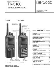
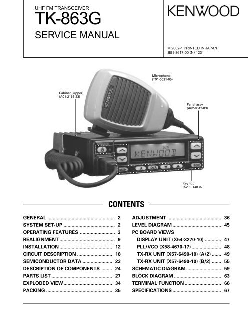
UHF FM TRANSCEIVER<br />
<strong>TK</strong>-863G<br />
SERVICE MANUAL<br />
© 2002-1 PRINTED IN JAPAN<br />
B51-8617-00 (N) 1231<br />
Microphone<br />
(T91-0621-05)<br />
Cabinet (Upper)<br />
(A01-2165-23)<br />
Panel assy<br />
(A62-0642-03)<br />
Key top<br />
(K29-9140-02)<br />
CONTENTS<br />
GENERAL .................................................. 2<br />
SYSTEM SET-UP ...................................... 2<br />
OPERATING FEATURES .......................... 3<br />
REALIGNMENT ......................................... 9<br />
INSTALLATION ....................................... 12<br />
CIRCUIT DESCRIPTION .......................... 18<br />
SEMICONDUCTOR DATA ...................... 23<br />
DESCRIPTION OF COMPONENTS ........ 24<br />
PARTS LIST ............................................. 27<br />
EXPLODED VIEW.................................... 34<br />
PACKING ................................................. 35<br />
ADJUSTMENT ........................................ 36<br />
LEVEL DIAGRAM .................................... 45<br />
PC BOARD VIEWS<br />
DISPLAY UNIT (X54-3270-10) ............ 47<br />
PLL/VCO (X58-4670-17) ...................... 48<br />
TX-RX UNIT (X57-6490-10) (A/2) ....... 49<br />
TX-RX UNIT (X57-6490-10) (B/2) ....... 55<br />
SCHEMATIC DIAGRAM.......................... 59<br />
BLOCK DIAGRAM ................................... 63<br />
TERMINAL FUNCTION ........................... 66<br />
SPECIFICATIONS .................................... 67
<strong>TK</strong>-863G<br />
GENERAL / SYSTEM SET-UP<br />
INTRODUCTION<br />
SCOPE OF THIS MANUAL<br />
This manual is intended for use by experienced technicians<br />
familiar with similar types of commercial grade communications<br />
equipment. It contains all required service information<br />
for the equipment and is current as of the publication<br />
date. Changes which may occur after publication are<br />
covered by either Service Bulletins or Manual Revisions.<br />
These are issued as required.<br />
ORDERING REPLACEMENT PARTS<br />
When ordering replacement parts or equipment information,<br />
the full part identification number should be included.<br />
This applies to all parts : components, kits, or chassis. If the<br />
part number is not known, include the chassis or kit number<br />
of which it is a part, and a sufficient description of the required<br />
component for proper identification.<br />
PERSONNEL SAFETY<br />
The following precautions are recommended for personnel<br />
safety :<br />
• DO NOT transmit if someone is within two feet (0.6<br />
meter) of the antenna.<br />
• DO NOT transmit until all RF connectors are verified secure<br />
and any open connectors are properly terminated.<br />
• SHUT OFF and DO NOT operate this equipment near<br />
electrical blasting caps or in an explosive atmosphere.<br />
• All equipment should be properly grounded before<br />
power-up for safe operation.<br />
• This equipment should be serviced by a qualified technician<br />
only.<br />
SERVICE<br />
This radio is designed for easy servicing. Refer to the<br />
schematic diagrams, printed circuit board views, and alignment<br />
procedures contained in this manual.<br />
Note<br />
When you modify your radio as described in system setup,<br />
take the following precaution.<br />
The rating of pin 7 (SB) of the accessory connector cable<br />
(KCT-19) on the rear of the radio is 13.6V (1A). Insert a 1A<br />
fuse if you use the SB pin for external equipment.<br />
13<br />
15<br />
7<br />
6<br />
1<br />
3<br />
Accessory connector<br />
cable (KCT-19)<br />
If you do not intend to use the 3.5-mm jack for the external<br />
speaker, fit the supplied speaker-jack cap (B09-0235-05)<br />
to stop dust and sand getting in.<br />
+<br />
–<br />
SYSTEM SET-UP<br />
Merchandise received<br />
License and frequency allocated by FCC<br />
Choose the type of transceiver<br />
Transceiver programming (Option)<br />
Frequency range (MHz)<br />
450~490<br />
RF power<br />
25W<br />
Type<br />
K<br />
See page 10.<br />
A personal computer (IBM PC or compatible), programming interface (KPG-46),<br />
and programming software (KPG-76D) are required for programming.<br />
(The frequency and signalling (option) data are programmed for the transceiver.)<br />
KCT-35<br />
Connection cable<br />
(Option)<br />
KGP-2A Modem<br />
GPS receiver or<br />
KGP-2B Modem<br />
GPS controller<br />
(Option)<br />
KCT-20<br />
Connection cable<br />
(Option)<br />
KGP-1A Modem<br />
GPS receiver or<br />
KGP-1B Modem<br />
GPS controller<br />
(Option)<br />
KES-3<br />
External speaker<br />
Delivery<br />
See page 17. See page 12.<br />
See page 13.<br />
(Option)<br />
KCT-19<br />
Accessory connector cable<br />
(Option)<br />
KCT-18<br />
Ignition sense cable<br />
(Option)<br />
See page 14.<br />
KAP-1<br />
PA/HA unit<br />
(Option)<br />
See page 17.<br />
KES-4<br />
External speaker<br />
(Option)<br />
2
OPERATING FEATURES<br />
<strong>TK</strong>-863G<br />
1. Controls and Functions<br />
1-1. Front Panel<br />
1-3. Display<br />
1 2 3 4 5<br />
6<br />
1-2. Microphone<br />
q (Power) switch<br />
Press to switch the transceiver ON (or OFF).<br />
w LED indicator<br />
Lights red while transmitting.<br />
e / keys<br />
Press these keys to activate their programmable auxiliary<br />
functions (page 4). The default settings are Volume<br />
Up and Volume Down.<br />
r Display<br />
See right for more information.<br />
8<br />
t / keys<br />
Press these keys to activate their programmable auxiliary<br />
functions (page 4). The default settings are System<br />
Up and System Down.<br />
7<br />
Indicator<br />
1-4. Rear Panel<br />
Description<br />
Appears when the selected group is<br />
programmed as priority.<br />
Appears when the selected group is<br />
programmed as Talk Around.<br />
Appears when the key programmed<br />
as Monitor is pressed.<br />
If programmed by your dealer,<br />
appears when you receive an ID.<br />
Appears when you are using Scan<br />
mode.<br />
Appears when the auxiliary function<br />
is activated.<br />
In trunked operation, appears when<br />
the selected group is programmed<br />
as telephone IDs.<br />
Appears when the selected system<br />
is removed from the scanning<br />
sequence.<br />
Displays the system and group<br />
numbers. Your dealer can program<br />
system and group names with up to<br />
8 characters, in place of numbers.<br />
y Microphone jack<br />
Insert the microphone plug into this connector.<br />
u MON, A, D/A, , , and SCN keys<br />
Press these keys to activate their programmable auxiliary<br />
functions (page 4).<br />
i PTT switch<br />
To transmit, press and hold this switch, then speak into<br />
the microphone. Release to receive.<br />
Power input<br />
connector<br />
External<br />
speaker jack<br />
Antenna<br />
connector<br />
3
<strong>TK</strong>-863G<br />
OPERATING FEATURES<br />
1-5. Programmable Auxiliary Functions<br />
You can program the / (left side), / (right side),<br />
MON, A, D/A, , , and SCN keys with the functions listed<br />
below.<br />
• AUX<br />
• Display Character<br />
• DTMF ID (BOT)<br />
• DTMF ID (EOT)<br />
• Emergency * 1<br />
• Group Down<br />
• Group Up<br />
• <strong>Home</strong> Group<br />
• Horn Alert<br />
• Key Lock<br />
• Memory (RCL)<br />
• Memory (RCL/STO)<br />
• Memory (STO)<br />
• Monitor Momentary<br />
• Monitor Toggle<br />
• None (No function)<br />
• Public Address<br />
• Redial<br />
• Scan<br />
• Scan Del/Add<br />
• Scan Temporary Delete<br />
• Squelch Off Momentary<br />
• Squelch Off Toggle<br />
• System Down<br />
• System Up<br />
• Telephone Disconnect<br />
• Volume Down<br />
• Volume Up<br />
*1 : This function can be used only with a foot switch.<br />
2. Operation Features<br />
The <strong>TK</strong>-863G is a UHF FM radio designed to operate in<br />
trunking format. The programmable features are summarized.<br />
3. Transceiver Controls and Indicators<br />
3-1. Front Panel Controls<br />
All the keys on the front panel are momentary-type push<br />
buttons. The functions of these keys are explained below.<br />
• POWER key<br />
Transceiver POWER key. When the power is switched<br />
off, all the parameters are stored in memory. When the<br />
power is switched on again, the transceiver returns to the<br />
previous conditions.<br />
• SYSTEM UP/DOWN key (Programmable)<br />
• / key (Programmable)<br />
• SCAN key (Programmable)<br />
• MONITOR key (Programmable)<br />
• A, D/A key (Programmable)<br />
• VOLUME UP/DOWN key (Programmable)<br />
• TX LED<br />
The TX indicator (Red LED) shows that you are transmitting.<br />
3-2. Programmable Keys<br />
The FPU (KPG-76D) enables programmable keys to select<br />
the following functions.<br />
None, AUX, DTMF ID (BOT), DTMF ID (EOT), Display<br />
Character, Emergency, Group Down, Group Up, <strong>Home</strong><br />
Group, Horn Alert, Key Lock, Memory (RCL/STO), Memory<br />
(RCL), Memory (STO), Monitor Momentary, Monitor Toggle,<br />
Public Address, Redial, Scan, Scan Del/Add, Scan Temporary<br />
Delete, Squelch Off Momentary, Squelch Off Toggle,<br />
System Down, System Up, Telephone Disconnect, Volume<br />
Down and Volume Up.<br />
• AUX<br />
If this key is pressed, “AUX” icon lights on the display<br />
and AUX port which is inside of the transceiver turns to the<br />
active level. If pressed again, the “AUX” icon goes off and<br />
the AUX ports turns to the lower level.<br />
• Display character<br />
This key switches the LCD display between the system<br />
and group number and the system and group name.<br />
• DTMF ID (BOT)<br />
In conventional mode, if you press this key, a predetermined<br />
DTMF ID (Begin of TX) will be sent automatically.<br />
• DTMF ID (EOT)<br />
In conventional mode, if you press this key, a predetermined<br />
DTMF ID (End of TX) will be sent automatically.<br />
• Emergency<br />
Pressing this key for longer than the programmed “Emergency<br />
Key Delay Time” causes the transceiver to enter the<br />
Emergency mode and display the “Emergency Display” setting.<br />
The transceiver automatically switches to the “Emergency<br />
System/Group” and transmits for the programmed<br />
“Duration of Transmission Mode”.<br />
The transceiver disables MIC mute while transmitting.<br />
After finishing transmission, the transceiver receives for the<br />
programmed “Duration of Receiving Mode”. The transceiver<br />
mutes the speaker while receiving.<br />
4
OPERATING FEATURES<br />
<strong>TK</strong>-863G<br />
Following the above sequence, the transceiver continues<br />
to transmit and receive. While in Emergency mode, switch<br />
the power OFF or press [Emergency] for longer than the programmed<br />
“Emergency Key Delay Time” to exit Emergency<br />
mode.<br />
Note : This function can be assigned to only the Foot<br />
switch.<br />
• Group up/down<br />
When the key is pressed each time, the group number to<br />
be selected is incremented/decremented and repeats if held<br />
for one second or longer.<br />
• <strong>Home</strong> group<br />
Each pressing of the key selects a preset system/group.<br />
• Horn alert<br />
If you are called from the base station or other party using<br />
signalling for Horn Alert function selected in a group, while<br />
you are away from your transceiver, you will be alerted by<br />
the vehicle horn or some other type of external alert. To turn<br />
the horn alert function on , press this key. A confirmation<br />
tone sounds.<br />
If this key is pressed again, the horn alert function is<br />
turned off.<br />
• Key lock<br />
Pressing this key causes the transceiver to accept entry<br />
of only the [Vol Up/Down], [Key lock], [PTT], [Monitor Momentary],<br />
[Monitor Toggle], [Squelch Off Momentary],<br />
[Squelch Off Toggle], and [Emergency] keys.<br />
• Memory<br />
This key allows DTMF memory data to be recalled; up to<br />
32 memories each with a memory dial of up to 16 digits and<br />
an A/N of up to 8 digits per memory.<br />
• Monitor<br />
Used to release signalling or squelch when operating as a<br />
conventional.<br />
• None<br />
Sounds error operation beep, and no action will occur.<br />
Use this function when the transceiver is required to be<br />
more simple operated.<br />
• Public address<br />
Public address amplifies the microphone audio, and outputs<br />
it through a PA speaker. PA is activated by pressing<br />
this key. A confirmation tone sounds, (and the display<br />
shows “PA”). PA can be activated at anytime (scanning or<br />
non-scanning).<br />
If this key is pressed again, a confirmation tone will<br />
sound, (the display will return to the normal group or SCAN<br />
display), and the PA function will turn off.<br />
• Redial<br />
If you press this key when the system/group is displayed,<br />
the last transmitted DTMF code will appear on the display.<br />
Pressing the PTT switch at this time will transmit the displayed<br />
DTMF code.<br />
• Scan<br />
Press this key starts scanning. Pressing this key stops<br />
scanning.<br />
• Scan del/add<br />
Used to select whether system scan routines are used<br />
during system scan. Each pressing of the key (to ON)<br />
toggles between lockout and lock. The scan routine is<br />
started when on lock. The DEL indicator flashes when the<br />
system is on lockout.<br />
• Scan temporary delete<br />
This key is temporarily deleted a system being scanned.<br />
If you press this key when scan is stopped (when a call is<br />
being received from another station), the system is temporarily<br />
deleted and scanning restarts.<br />
This key operates even when “Scan Type” is set to “List<br />
Type System Scan”.<br />
• System up/down<br />
When the key is pressed each time, the system number<br />
to be selected is incremented/decremented and repeats if<br />
held for one second or longer.<br />
• Telephone disconnect<br />
Pressing this key ends an RIC connection (disconnects<br />
the telephone line).<br />
• Volume up/down<br />
When the key is pressed, the volume level is increased/<br />
decreased and repeats if held for 200ms or longer.<br />
4. Scan Operating<br />
■ System Scan<br />
System scan can be selected with the “Scan” key by programming<br />
the scan feature. When the “Scan” key is<br />
pressed and the “SCN” mark appears, scan mode in entered.<br />
Scanning starts from the system following the currently<br />
displayed system. When a call is received, scanning<br />
stops, and the system and group are displayed.<br />
When programming key is touched during scanning, the<br />
scan stops and the revert system or group can be changed.<br />
Scanning resumes one second after the key is released.<br />
There are two types of system scan.<br />
• Fix system scan<br />
All the set systems except locked-out ones are scanned.<br />
If the Del/Add feature is assigned to the programmable key,<br />
it can be controlled from the front panel.<br />
5
<strong>TK</strong>-863G<br />
OPERATING FEATURES<br />
• List type system scan<br />
A scan list can be set for each system.<br />
The list to be scanned can be changed by changing the<br />
display system.<br />
If many systems have been set, the scan speed can be<br />
increased by narrowing the systems to be scanned with<br />
scan lists.<br />
■ System Lockout<br />
The system lockout feature is used to lock systems out<br />
of the scan sequence, and can be selected by programming<br />
in the following two ways;<br />
• Fixed lockout<br />
The system to be locked out is selected by programming.<br />
When a locked system is selected, the Delete ( ) indicator<br />
appears on the left of the SYSTEM indicator. The revert system<br />
is scanned even if it is locked out. If there is a locked<br />
system, the Delete ( ) indicator flashes during fixed scanning.<br />
• User selectable lockout<br />
If the scan lockout feature is programmed to a key, the<br />
user can lock systems out of the scan sequence with the<br />
key. To lock a system out of the scan sequence, press the<br />
key when the system is displayed. The Delete ( ) indicator<br />
is displayed on the left of the SYSTEM indicator.<br />
To unlock a system, select the system and press the key.<br />
The Delete ( ) indicator disappears to indicate that the system<br />
has returned to the scan sequence. The revert system<br />
is scanned even if it is locked out. If there a locked system,<br />
the Delete ( ) indicator flashes during fixed scanning. If all<br />
systems are locked out, the scan stops and only the revert<br />
system is received.<br />
■ Drop-out Delay Time (Scan Resume Time)<br />
If a call is received during scan, the scan stops. The scan<br />
resume time can be programmed as 0 to 300 seconds in<br />
one-second increments. The default value is 3 seconds.<br />
■ Dwell Time<br />
The dwell time is the time after transmission ends until<br />
the scan resumes in scan mode. It can be set 0 to 300 seconds<br />
by programming. The default value is 3 seconds.<br />
■ System/Group Revert<br />
System/group revert can be programmed for one of the<br />
following;<br />
• Last called revert<br />
The system or group changes to the revert system or<br />
group when a call is received with the system or group being<br />
scanned.<br />
• Last used revert<br />
If a system/group call is received during scanning and the<br />
PTT button is pressed for transmission and response within<br />
the drop out delay time, the system or group is assigned as<br />
the new revert system or group.<br />
• Selected revert<br />
If the system/group was changed while scanning, the<br />
newly selected system/group.<br />
• Selected + Talkback revert<br />
If the system/group was changed while scanning, the<br />
newly selected system/group. The transceiver “talks back”<br />
on the current receive group.<br />
■ Scan Massage Wait<br />
The time for staying with the home repeater that receives<br />
a signal during system scan and monitoring data<br />
messages can be programmed. If there is no signal from<br />
the home repeater, the system is scanned for about 50ms.<br />
If there is a signal, three data messages are monitored.<br />
Normally, three data messages are monitored for each system,<br />
and it can be increased in multiples of three data messages<br />
per line to up to eight lines.<br />
If the repeater data message indicates that there is no<br />
call, data monitoring is terminated and the home repeater of<br />
the next system is scanned.<br />
■ Group Scan Operation<br />
Group scan can be programmed for each group. In addition<br />
to the ID codes of the selected group, the ID codes of<br />
the other groups that are permitted for group scan are decoded.<br />
(The two fixed ID and block decode codes are always<br />
decoded.)<br />
If, during group scanning, a call is received with one of<br />
the selectable group ID codes for which group scan is enabled,<br />
the group display indicates the group number that the<br />
call came in with. That group then becomes the new selected<br />
group. Group scan resumes after the specified dropout<br />
delay time or dwell time shared by the system scan<br />
elapses.<br />
■ In Conventional System<br />
If QT or DQT is set for the channel, the channels, including<br />
signalling, are scanned.<br />
In case of the priority group is set in conventional system,<br />
if a group scan (including group scan during a system<br />
scan) temporarily stops (receiving) in a group that does not<br />
have priority, a look back is performed to the priority group.<br />
Look back is performed according to the look back time A<br />
and B settings. If a call is received on the priority group,<br />
reception immediately switches to the priority group.<br />
6
OPERATING FEATURES<br />
<strong>TK</strong>-863G<br />
5. Details of Features<br />
■ Time-out Timer<br />
The time-out timer can be programmed in 15 seconds<br />
increments from 15 seconds to ten minutes. If the transmitter<br />
is keyed continuously for longer than the programmed<br />
time, the transmitter is disabled and a warning tone sounds<br />
while the PTT button is held down. The alert tone stops<br />
when the PTT button is released.<br />
■ PTT ID<br />
PTT ID provides a DTMF ANI to be sent with every time<br />
PTT (beginning of transmission, end of transmission, or<br />
both).<br />
You can program PTT ID “on” or “off” for each group.<br />
The contents of ID are programmed for each transceiver.<br />
The timing that the transceiver sends ID is programmable.<br />
BOT : DTMF ID (BOT) is sent on beginning of transmission.<br />
EOT : DTMF ID (EOT) is sent on end of transmission.<br />
Both : DTMF ID (BOT) is sent on beginning of transmission<br />
and DTMF ID (EOT) is sent on end of transmission.<br />
■ Radio Password<br />
When the password is set in the transceiver, user can not<br />
use the transceiver unless enter the correct password.<br />
This code can be up to 6 digits from 0 to 9 and input with<br />
the key, and "SCN" key.<br />
■ Off Hook Decode<br />
If the Off hook decode function has been enabled, removing<br />
and replacing the microphone on the hook has no<br />
effect for decoding QT/DQT.<br />
■ Horn Alert<br />
Horn alert can be set to on or off for each group. If horn<br />
alert has been set to YES for a group and DEC ID/QT/DQT<br />
matches, the horn alert, HOR. is turned on and off.<br />
Either continuous or non-continuous operation can be set<br />
by the FPU. The horn alert port is enabled or disabled as<br />
follows;<br />
Off hook horn alert Hook off Hook on<br />
Enable Yes Yes<br />
Disable No Yes<br />
■ Pulse<br />
The horn alert port, HOR, is turned on and off as follows;<br />
0.5s 0.5s 0.5s 0.5s 0.5s<br />
HOR<br />
The timing when the fixed LTR ID matches is as follows<br />
(trunking mode);<br />
1s 0.5s 1s<br />
■ Continuous<br />
Horn alert can be reset by setting an expiration time from<br />
the FPU, pressing the Horn Alert key, or setting off hook.<br />
■ Data TX with QT/DQT<br />
Whether programmed QT/DQT is modulated or not with<br />
a data transmission. A radio unit can receive a data message<br />
regardless of QT/DQT if the receiving unit is not scanning.<br />
■ Call Indicator<br />
The call indicator can be programmed for each group. In<br />
trunked system, it can be set to respond to a selectable decode<br />
ID or one of two fixed IDs, except block IDs. When a<br />
call is received with a selectable decode ID, the call indicator<br />
flashes. When a call is received with a fixed ID, the call<br />
indicator lights continuously.<br />
On a conventional system, the call indicator can be programmed<br />
to light for each QT or DQT code. It keeps flashing<br />
while a call is being received. It is turned off by pressing<br />
any front panel key.<br />
■ Free System Ringback<br />
This feature is available only when a telephone interconnected<br />
ID code is selected. If a busy tone sounds when the<br />
PTT button is pressed, the transceiver enters this mode automatically.<br />
When the PTT button is released, a beep sounds for<br />
400ms to indicate that the mode has been entered. If the<br />
scan is on, it is resumed (the “SCN” mark goes on). When<br />
any repeater becomes available, a ringing tone sounds and<br />
this mode ends.<br />
The mode is terminated when the system, group, scan,<br />
PTT, key is changed.<br />
■ System Search<br />
This feature can be programmed to automatically access<br />
other programmed systems when the selected system cannot<br />
be accessed. If an intercept tone sounds when the PTT<br />
button is pressed after setting the mode, the transceiver<br />
has entered the mode.<br />
If the group ID is a telephone interconnect ID, the transceiver<br />
then attempts to access, in succession, other systems<br />
that have a telephone interconnect ID in the revert<br />
group location. If the group ID is a dispatch ID, the transceiver<br />
attempts to access other systems that have a dispatch<br />
ID programmed in the revert group location.<br />
7
<strong>TK</strong>-863G<br />
OPERATING FEATURES<br />
If there is no system to be accessed, an intercept tone<br />
sounds, the mode is terminated, and the transceiver returns<br />
to the first system. If the access is successful, the mode is<br />
terminated, and the searched system becomes the new selected<br />
system (If during scanning, the scan stops).<br />
■ Transpond<br />
This feature can be programmed to turn on and off for<br />
each group. If the ID of the group for which transpond is<br />
enabled is received, two data messages (transmit ID and<br />
turn-off code) are automatically transmitted if the PTT button<br />
is not pressed as a response within the time set (0 to<br />
300 seconds in 1-second increments). If the PTT button is<br />
pressed within the time, the transpond is not preformed.<br />
■ Transmit Inhibit<br />
The transceiver can be programmed with a transmit inhibit<br />
block of ID codes. If an ID code within this block is<br />
decoded the preset time before the PTT button is pressed,<br />
transmission is inhibited. The BUSY indicator lights and a<br />
busy tone sounds until the PTT button is released to indicate<br />
that transmission is not possible (except clear-to talk mode).<br />
■ ARQ Mode<br />
It affects Trunking mode only. Automatic Repeat<br />
reQuest (ARQ) mode is a manner to minimize the air traffic<br />
of data communication. Also, it enables to occupy the<br />
trunking repeater channel for the data communication period.<br />
6. Audible User Feedback Tones<br />
The transceiver outputs various combinations of tones to<br />
notify the user of the transceiver operating state. The main<br />
tones are listed below.<br />
The high tone is 1477Hz, the mid tone is 941Hz, and the<br />
low tone is 770Hz.<br />
■ Power On Tone<br />
This tone is output when the transceiver is turned on.<br />
(The high tone is output for 500ms.)<br />
■ Alert Tone<br />
This tone is output when the transceiver is TX inhibition<br />
for TOT, and PLL unlocked. It is output until the PTT button<br />
is released.<br />
■ Password Agreement Tone<br />
When the correct password is entered, the tone sounds.<br />
The optional feature’s control tone can be set to yes or no.<br />
■ PTT Release Tone<br />
When you release the PTT switch, the PTT release tone<br />
sounds.<br />
■ Busy Tone<br />
Sounds in LTR mode, when you cannot use a repeater<br />
(system busy or TX inhibit). Sounds in conventional mode,<br />
when busy channel lockout is functioning. You can select<br />
yes or no for the optional feature’s warning tone.<br />
■ Key Press Tone [A]<br />
Sounds when a key is pressed. For toggle keys, sounds<br />
when toggle function is turned on (key press tone [B]<br />
sounds when it is turned off). You can select yes or no for<br />
the optional feature’s control tone.<br />
■ Key Press Tone [B]<br />
Sounds when a key is pressed. For toggle keys, sounds<br />
when the toggle function is turned off (key press tone [A]<br />
sounds when it is turned on). You can select yes or no for<br />
the optional feature’s control tone.<br />
■ Key Press Tone [C]<br />
Sounds when a key is pressed. Also sounds when storing<br />
data, adding a DTMF code to memory, and when changing<br />
test mode settings. You can select yes or no for the<br />
optional feature’s control tone.<br />
■ Key Input Error Tone<br />
Sounds when a key is pressed but that key cannot be<br />
used. You can select yes or no for the optional feature’s<br />
warning tone.<br />
■ Roll Over Tone<br />
Sounds at the smallest system/group. You can select<br />
yes or no for the optional feature’s control tone.<br />
■ Transpond Tone<br />
Sounds when an individual call with the correct LTR ID is<br />
received.<br />
■ Intercept Tone<br />
This tone indicates that the transceiver is out of range. It<br />
indicates that the PTT button is pressed, and transmission<br />
has started, but the repeater cannot be connected and talking<br />
is not possible. It is output until the PTT button is released.<br />
(The mid tone and low tone are output alternately in<br />
200ms intervals.)<br />
■ Delay Tone<br />
This tone is output when the PTT button is pressed and<br />
the repeater is accessed three times or more to indicate<br />
connection with the repeater is delayed. This tone is the<br />
same as the busy tone. (It is not output of clear to talk has<br />
been set to yes.)<br />
8
OPERATING FEATURES / REALIGNMENT<br />
<strong>TK</strong>-863G<br />
■ Proceed Tone<br />
This tone is output when the PTT button is pressed,<br />
transmission starts, and the repeater is connected to indicate<br />
that the user can talk if the clear to talk function has<br />
been set. (The high tone is output for 100ms.)<br />
REALIGNMENT<br />
1. Modes<br />
User mode<br />
■ Free System Ringback Mode Tone, System<br />
Search Mode Tone<br />
This tone indicates that the transceiver is free system<br />
ringback mode or system search mode. (The mid tone is<br />
output for 400ms.)<br />
Panel test mode<br />
PC mode<br />
Firmware programming<br />
mode<br />
Panel tuning mode<br />
Data programming<br />
mode<br />
PC test mode<br />
PC tuning mode<br />
■ Ringing Tone<br />
This tone indicates that the transceiver can use the repeater<br />
in free system ringback mode. (The mid tone and no<br />
tone are output eight cycles alternately in 50ms intervals.)<br />
■ System Search Tone<br />
Sounds when the system changes during system search.<br />
You can select yes or no for the optional feature's warning<br />
tone.<br />
■ System Search End Tone<br />
Sounds when a possible connection to a repeater in system<br />
search is not mode. You can select yes or no for the<br />
optional feature’s warning tone.<br />
Clone mode<br />
Mode<br />
User mode<br />
Panel test mode<br />
Panel tuning mode<br />
PC mode<br />
Data programming<br />
mode<br />
PC test mode<br />
Firmware programming<br />
mode<br />
Clone mode<br />
Radio information<br />
Function<br />
For normal use.<br />
Used by the dealer to check the fundament<br />
characteristics.<br />
Used by the dealer to tune the radio.<br />
Used for communication between the<br />
radio and PC (IBM compatible).<br />
Used to read and write frequency data<br />
and other features to and from the radio.<br />
Used to check the radio using the PC.<br />
This feature is included in the FPU.<br />
See panel tuning.<br />
Used when changing the main program<br />
of the flash memory.<br />
Used to transfer programming data from<br />
one radio to another.<br />
2. How to Enter Each Mode<br />
Mode<br />
Operation<br />
User mode<br />
Power ON<br />
Panel test mode<br />
[SCN]+Power ON (Two seconds)<br />
PC mode<br />
Received commands from PC<br />
Panel tuning mode<br />
[Panel test mode]+[SCN]<br />
Firmware programming mode [ ]+Power ON (Two seconds)<br />
Clone mode [ ]+Power ON (Two seconds)<br />
3. For the Panel Test Mode<br />
Setting method refer to ADJUSTMENT.<br />
3-1. For the Panel Tunning Mode<br />
Setting method refer to ADJUSTMENT.<br />
9
<strong>TK</strong>-863G<br />
REALIGNMENT<br />
4. Radio Information<br />
Executing this function, “–PC–” apears on the display of<br />
the <strong>TK</strong>-863G while calculation the check sum.<br />
When the calculation is completed, the display returns to<br />
normal and PC displays the check sum of the radio.<br />
5. PC Mode<br />
5-1. Preface<br />
The <strong>TK</strong>-863G transceiver is programmed using a personal<br />
computer, a programming interface (KPG-46) and programming<br />
software (KPG-76D).<br />
The programming software can be used with an IBM PC<br />
or compatible. Figure 1 shows the setup of an IBM PC for<br />
programming.<br />
5-2. Connection Procedure<br />
1. Connect the <strong>TK</strong>-863G to the personal computer with the<br />
interface cable.<br />
2. When the Power is switched on, user mode can be entered<br />
immediately. When the PC sends a command, the<br />
radio enters PC mode.<br />
When data is transmitted from transceiver, the red LED<br />
blink.<br />
When data is received by the transceiver, the green LED<br />
blink.<br />
Notes :<br />
• The data stored in the personal computer must match<br />
model type when it is written into the flash memory.<br />
• Change the <strong>TK</strong>-863G to PC mode, then attach the interface<br />
cable.<br />
5-3. KPG-46 Description<br />
(PC programming interface cable : Option)<br />
The KPG-46 is required to interface the <strong>TK</strong>-863G to the<br />
computer. It has a circuit in its D-subconnector (25-pin) case<br />
that converts the RS-232C logic level to the TTL level.<br />
The KPG-46 connects the modular microphone jack of<br />
the <strong>TK</strong>-863G to the computers RS-232C serial port.<br />
IBM-PC<br />
KPG-46<br />
5-4. Programming Software Description<br />
The KPG-76D programming disk is supplied in 3-1/2" disk<br />
format. The software on this disk allows a user to program<br />
<strong>TK</strong>-863G radio via a programming interface cable (KPG-46).<br />
5-5. Programming With IBM PC<br />
If data is transferred to the transceiver from an IBM PC<br />
with the KPG-76D, the destination data (basic radio information)<br />
for each set can be modified. Normally, it is not necessary<br />
to modify the destination data because their values are<br />
determined automatically when the frequency range (frequency<br />
type) is set.<br />
The values should be modified only if necessary. Data<br />
can be programmed into the flash memory in RS-232C format<br />
via the modular microphone jack.<br />
6. Firmware Programming Mode<br />
6-1. Preface<br />
Flash memory is mounted on the <strong>TK</strong>-863G. This allows<br />
the <strong>TK</strong>-863G to be upgraded when new features are released<br />
in the future. (For details on how to obtain the firmware,<br />
contact Customer Service.)<br />
6-2. Connection Procedure<br />
Connect the <strong>TK</strong>-863G to the personal computer (IBM PC<br />
or compatible) with the interface cable (KPG-46). (Connection<br />
is the same as in the PC Mode.)<br />
6-3. Programming<br />
1. Start up the programming software (FPRO EXE.).<br />
2. Set the communications speed (normally, 57600 bps)<br />
and communications port in the Setup item.<br />
3. Set the firmware to be updated by file name item.<br />
4. Turn the <strong>TK</strong>-863G Power ON with the [ ] switch held<br />
down. Hold the switch down for two seconds until the<br />
display changes to “PROG 576”, the BUSY/TX LED lights<br />
orange. When “PROG 576” appears, release your finger<br />
from the switch.<br />
5. Check the connection between the <strong>TK</strong>-863G and the personal<br />
computer, and make sure that the <strong>TK</strong>-863G is in<br />
Program mode.<br />
6. Click write button in the window. A window opens on<br />
the display to indicate the writing progress. When the<br />
<strong>TK</strong>-863G starts to receive data, the BUSY/TX LED lights<br />
green.<br />
7. If writing ends successfully, the LED on the <strong>TK</strong>-863G<br />
goes off and the checksum is displayed.<br />
8. If you want to continue programming other <strong>TK</strong>-863G, repeat<br />
steps 4 to 7.<br />
KPG-76D<br />
Fig. 1<br />
<strong>TK</strong>-863G<br />
Notes :<br />
• This mode cannot be entered if the Firmware programming<br />
mode is set to Disable in the Programming software<br />
(KPG-76D).<br />
• When programming the firmware, it is recommend to<br />
copy the data from the floppy disk to your hard disk before<br />
you update the radio firmware.<br />
Directly copying from the floppy disk to the radio may not<br />
work because the access speed is too slow.<br />
10
REALIGNMENT<br />
<strong>TK</strong>-863G<br />
6-4. Function<br />
1. If you press the [MON] switch while “PROG 576” is displayed,<br />
the checksum is displayed. If you press the<br />
[MON] switch again (while the checksum is displayed),<br />
“PROG 576” is redisplayed.<br />
2. If you press the [A] switch while “PROG 576” is displayed,<br />
the display changes to “PROG 192” to indicate<br />
that the write speed is low speed (19200 bps). If you<br />
press the [A] switch again while “PROG 192” is displayed,<br />
the display changes to “PROG 384”, and the<br />
write speed becomes the middle speed (38400 bps). If<br />
you press the [A] switch again while “PROG 384” is displayed,<br />
the display returns to “PROG 576”.<br />
Note :<br />
Normally, write in the high-speed mode.<br />
4. Power on the slave <strong>TK</strong>-863G.<br />
5. Connect the cloning cable (No. E30-3382-05) to the<br />
modular microphone jacks on the master and slave.<br />
6. Press the [SCN] key on the master while the master displays<br />
“CLONE”. The data of the master is sent to the<br />
slave. While the slave is receiving the data, “–PC–” is<br />
displayed. When cloning of data is completed, the master<br />
displays “END”, and the slave automatically operates<br />
in the User mode. The slave can then be operated by the<br />
same program as the master.<br />
7. The other slave can be continuously cloned. When the<br />
[SCN] key on the master is pressed while the master displays<br />
“END”, the master displays “CLONE”. Carry out<br />
the operation in step 4 to 6.<br />
7. Clone Mode<br />
Programming data can be transferred from one radio to<br />
another by connecting them via their modular microphone<br />
jacks. The operation is as follows (the transmit radio is the<br />
master and the receive radio is the slave).<br />
1. Turn the master <strong>TK</strong>-863G power ON with the [ ] key<br />
held down. If the password is set to the <strong>TK</strong>-863G, the<br />
<strong>TK</strong>-863G displays “CLN LOCK”. If the password is not<br />
set, the <strong>TK</strong>-863G displays “CLONE”.<br />
2. When “CLN LOCK” is displayed, only the [ / ] key and<br />
[SCN], and [0] to [9] keys can be accepted. When you<br />
enter the correct password, and “CLONE” is displayed,<br />
the <strong>TK</strong>-863G can be used as the cloning master. The following<br />
describes how to enter the password.<br />
3. How to enter the password with the microphone keypad;<br />
If you press a key while “CLN LOCK” is displayed, the<br />
number that was pressed is displayed on the <strong>TK</strong>-863G.<br />
Each press of the key shifts the display in order to the<br />
left. When you enter the password and press the [SCN]<br />
key, “CLONE” is displayed if the entered password is<br />
correct. If the password is incorrect, “CLN LOCK” is<br />
redisplayed.<br />
How to enter the password with the [ / ] key;<br />
If the [ / ] key is pressed while “CLN LOCK” is displayed,<br />
numbers (0 to 9) are displayed flashing. When<br />
you press the [SCN] key, the currectly selected number is<br />
determined, and the display shifts to the left. If you press<br />
the [SCN] key after entering the password in this procedure,<br />
“CLONE” is displayed if the entered password is<br />
correct. If the password is incorrect, “CLN LOCK” is<br />
redisplayed.<br />
Cloning cable<br />
(E30-3382-05)<br />
Fig. 2<br />
11
<strong>TK</strong>-863G<br />
INSTALLATION<br />
1. Accessory Connection Cable<br />
(KCT-19 : Option)<br />
The KCT-19 is an accessory connection cable for connecting<br />
external equipment. The connector has 15 pins and<br />
the necessary signal lines are selected for use.<br />
1-1. Installing the KCT-19 in the transceiver<br />
1. Remove the upper and lower halves of the transceiver<br />
case, and lift the DC cord bushing ( 1 ) from the chassis.<br />
2. Remove the pad as shown in Figure 1 ( 2 ).<br />
3. Insert the KCT-19 cable ( 3 ) into the chassis ( 4 ).<br />
The wire harness band ( 5 ) must be inside the chassis.<br />
4. Replace the DC cord bushing ( 6 ).<br />
5. Connect the KCT-19 to the TX-RX unit (A/2) as shown in<br />
Figure 2 ( 7 ).<br />
6. Connect the KCT-19 to the external accessory by inserting<br />
the crimp terminal ( 8 ) into the square plug ( 9 ),<br />
both of which are supplied with the KCT-19.<br />
1<br />
2<br />
1-2. KCT-19 Accessory Port Function<br />
No. No. Name Function Note<br />
(A) (B,C,D,E)<br />
1 D-2 DTC Data channel control/ *1<br />
External hook input<br />
2 D-5 ME External microphone ground<br />
3 D-3 IGN Ignition sense input<br />
4 D-1 DEO Receiver detector output<br />
5 D-6 MI External microphone input<br />
6 B-2 E Ground<br />
7 B-3 SB Switched B+, DC 13.6V output.<br />
Maximum 1A<br />
8 D-7 PTT External PTT input *1<br />
9 D-4 DI Data modulation input<br />
10 B-1 HOR Horn alert/call output<br />
11 D-8 SQ Squelch detect output *1<br />
12 C-1 SP Speaker audio output<br />
13 E-1 AM Speaker mute input, active high<br />
14 E-2 MM MIC mute input, active high<br />
15 E-3 EMG Foot switch input, active low *2<br />
TXS/LOK Transmitter sense output, active high *3<br />
*1 : MDT mode<br />
*2 : Emergency mode<br />
*3 : Foot switch setting : None<br />
Fig. 1<br />
D<br />
E<br />
B<br />
C<br />
CN5<br />
CN3<br />
CN4<br />
E<br />
C<br />
B<br />
D<br />
5<br />
4<br />
7<br />
CN8<br />
6<br />
3<br />
A<br />
9 Square plug<br />
(E09-1571-05)<br />
1<br />
13 3<br />
Contact<br />
15 12 8<br />
Crimp terminal<br />
(E23-0613-05)<br />
12<br />
Fig. 2
INSTALLATION<br />
<strong>TK</strong>-863G<br />
2. Accessory Terminal (TX-RX Unit)<br />
2-1. External Connector Accessory Terminal Method<br />
No. Name I/O Description Note<br />
CN1 1 8C O DC 8V output<br />
2 5S O DC 5V output<br />
3 AUX5 O<br />
4 AUX6 O Auxiliary output<br />
5 NC – Non-connection<br />
6 AUX3 O SQ : Squelch detect output *1<br />
7 AUX1 I PTT : External PTT input *1<br />
8 AUX4 TXD<br />
9 AUX2 RXD<br />
I DTC : Data channel control/<br />
External hook input<br />
10 ALT I Alert tone input<br />
11 AFO O Receiver audio signal output<br />
12 AFI I Receiver audio signal input<br />
13 MII I Transmit audio signal input<br />
14 MIO O Transmit audio signal output<br />
15 GND – Ground<br />
CN3 1 HOR O Horn alert/call output<br />
2 E – Ground<br />
3 SB O Switched B+, DC 13.6V<br />
output, Maximum 1A<br />
CN4 1 DEO O Receiver detector output<br />
Level : 0.35Vrms<br />
(Standard modulation)<br />
2 DTC I Data channel control/<br />
External hook input<br />
3 IGN I Ignition sense input<br />
4 DI I Data modulation input<br />
5 ME – External microphone ground<br />
6 MI I External microphone input<br />
7 PTT I External PTT input, active low<br />
8 SQ O Squelch detect output<br />
CN5 1 AM I Speaker mute input, active high<br />
2 MM I MIC mute input, active high<br />
3 EMG I Foot switch input, active low *2<br />
TXS/LOK O *3<br />
CN7 1 PA/LI O Relay for PA function KAP-1<br />
control<br />
O PA/LI ON : High, PA/LI OFF : Low<br />
2 SPO O Audio signal output to KAP-1<br />
3 SPI I Audio signal input from KAP-1<br />
CN8 1 SP O Audio signal output to<br />
internal/external speaker<br />
2 E – Ground<br />
*1 : MDT mode<br />
*2 : Emergency mode<br />
*3 : Foot switch setting : None<br />
3. Ignition Sense Cable (KCT-18 : Option)<br />
The KCT-18 is an optional cable for enabling the ignition<br />
function. The ignition function lets you turn the power to the<br />
transceiver on and off with the car ignition key.<br />
If you use the Horn Alert function or the Manual Relay<br />
function, you can turn the function off while driving with the<br />
ignition key.<br />
3-1. Connecting the KCT-18 to the Transceiver<br />
1. Install the KCT-19 in the transceiver. (See the KCT-19<br />
section.)<br />
2. Insert the KCT-18 lead terminal ( 2 ) into pin 3 of the<br />
square plug ( 1 ) supplied with the KCT-19, then insert<br />
the square plug into the KCT-19 connector ( 3 ).<br />
KCT-19<br />
3<br />
Fig. 3<br />
13<br />
15<br />
1<br />
1<br />
3 Contact<br />
6<br />
2<br />
KCT-18<br />
3-2. Modifying the Transceiver<br />
Modify the transceiver as follows to turn the power or<br />
the Horn Alert or Manual Relay function on and off with the<br />
ignition key.<br />
1. Remove the lower half of the transceiver case.<br />
2. Set jumper resistors (0Ω) R134 and R135 of the TX-RX<br />
unit (A/2) as shown in Table 1.<br />
KCT-19<br />
R133<br />
R134<br />
R135<br />
CN2<br />
Fig. 4<br />
TX-RX UNIT<br />
(A/2)<br />
ANT<br />
Operation when KCT-18 is connected R134 R135<br />
KCT-18 cannot be connected Enable Enable<br />
Power on/off and Horn Alert or AUX-A on/off Disable Enable<br />
Horn Alert or AUX-A on/off Enable Disable<br />
Power cannnot be turned on Disable Disable<br />
Table 1<br />
R134 and R135 setup chart<br />
13
<strong>TK</strong>-863G<br />
INSTALLATION<br />
4. PA/HA Unit (KAP-1 : Option)<br />
4-1. Installing the KAP-1 in the Transceiver<br />
The Horn Alert (max. 2A drive) and Public Address functions<br />
are enabled by inserting the KAP-1 W1 (3P; white/<br />
black/red) into CN3 on the TX-RX unit (A/2), inserting W2<br />
(3P; green) into CN7 on the TX-RX unit (A/2), and connecting<br />
the KCT-19 (option) to CN2 and CN3 of the KAP-1.<br />
• Installation procedure<br />
1. Open the upper case of the transceiver.<br />
2. Insert the two cables ( 1 ) with connectors from the<br />
KAP-1 switch unit into the connectors on the transceiver.<br />
3. Secure the switch unit board to the chassis with a screw<br />
( 3 ). The notch ( 2 ) in the board must be placed at the<br />
front left side.<br />
4. Attach the cushion on the top of the KAP-1 switch unit.<br />
3<br />
CN3<br />
1<br />
3<br />
W1 2<br />
W2<br />
Cushion<br />
(G13-1710-04)<br />
4<br />
1<br />
Fig. 6<br />
R1<br />
KAP-1 foil side view<br />
• Public address<br />
The signal from pin 13 of IC9 on the TX-RX unit (A/2)<br />
drives PA relay K1 in the KAP-1 and switches the audio<br />
power amplifier output between the external PA system<br />
(through KCT-19) and internal and external speakers.<br />
To use the PA function, R153 on the TX-RX unit (A/2)<br />
must be removed.<br />
Use the PA function<br />
Do not use the PA function<br />
R153<br />
Disable<br />
Enable<br />
CN1 CN2 KCT-19<br />
CN3<br />
CN7<br />
TX-RX UNIT<br />
(A/2)<br />
Fig. 5<br />
KCT-19<br />
CN2<br />
ANT<br />
R153<br />
Q19<br />
R122<br />
4-2. Modifying the Transceiver<br />
• Horn alert<br />
The signal from pin 4 of IC9 on the TX-RX unit (A/2) turns<br />
Q5 and Q1 on and off and drives KAP-1 HA relay K2 to drive<br />
the horn with a maximum of 2A.<br />
The default output is HR1. The relay open output can be<br />
obtained between HR1 and HR2 by removing R1 in the KAP-<br />
1.<br />
R1 Output form<br />
HR1 (Default) Enable<br />
HR1<br />
Fig. 7<br />
HR2<br />
Disable<br />
HR1<br />
HR2<br />
14
INSTALLATION<br />
<strong>TK</strong>-863G<br />
• Others<br />
If the PA and HR2 are not necessary and the speaker output<br />
is output to an external unit through the KCT-19, connect<br />
the KCT-19 C connector to CN8 on the TX-RX unit (A/2).<br />
TX-RX UNIT (A/2)<br />
IC9<br />
Shift<br />
register<br />
4<br />
Q1<br />
Q6<br />
13<br />
IGN<br />
Q5<br />
Q6<br />
8C<br />
R21<br />
Q1<br />
D2<br />
CN3<br />
W1<br />
HOR<br />
E<br />
SB<br />
KAP-1 (SWITCH UNIT : X41-3380-20)<br />
Q1 : DTD114EK<br />
D1,2 : 1SS193<br />
1<br />
2<br />
3<br />
R1 0<br />
C1<br />
1000P<br />
C5 1000P<br />
–<br />
K2<br />
+<br />
D1<br />
C6<br />
C7<br />
1000P<br />
1000P<br />
1<br />
2<br />
1<br />
2<br />
3<br />
CN1<br />
HR2<br />
NC<br />
CN2<br />
HR1<br />
E<br />
SB<br />
C<br />
B<br />
GRN<br />
BRN<br />
ORG<br />
YEL<br />
KCT-19<br />
R3 0<br />
K1<br />
C3 0.01<br />
1<br />
2<br />
CN3<br />
PAO/LIO<br />
E<br />
C<br />
GRN<br />
Audio<br />
power amp<br />
IC13<br />
+<br />
1<br />
2<br />
R153<br />
CN8<br />
CN7<br />
W2<br />
PA/LI<br />
SPO<br />
SPI<br />
1<br />
2<br />
3<br />
C2<br />
1000P<br />
R4 0<br />
Q1<br />
–<br />
+<br />
D2<br />
C4 0.01<br />
KCT-19 Terminal<br />
13 10 1<br />
15 12<br />
6<br />
3<br />
6 : Earth<br />
10 : HR1<br />
12 : PA (HR2)<br />
SP<br />
E<br />
Internal/External<br />
speaker<br />
Fig. 8<br />
5. Emergency Mode<br />
5-1. Transceiver Modification Procedure<br />
• Install the foot switch<br />
Install the foot switch through the KCT-19 and KCT-18.<br />
When the switch is treaded on, the radio enters the emergency<br />
mode.<br />
• Change the power switch circuit<br />
TX-RX unit (B/2) : Control section<br />
$R705 : Attach (R92-1252-05, 0Ω)<br />
TX-RX unit (A/2) : RF section<br />
R142 : Remove (RK73GB1J473J, 47kΩ)<br />
Once the transceiver is modified, it cannot be turned on<br />
and off with the power switch. The power switch turns the<br />
LCD backlight and display on and off. (The power is<br />
switched on and off by IGNITION SENSE.)<br />
SB Q505 Key<br />
backlight<br />
MBL<br />
MBL<br />
TX-RX section<br />
Q506<br />
KCT-19 Terminal<br />
13 1<br />
IC510<br />
6<br />
CN5<br />
LCD<br />
IC502 Attach<br />
CPU<br />
$R705<br />
87<br />
0<br />
88<br />
1 3<br />
KCT-19<br />
15 pin<br />
Foot<br />
switch<br />
25 20<br />
R142<br />
47K<br />
Remove<br />
IC14<br />
KCT-18<br />
Control section<br />
Power<br />
switch<br />
Outside<br />
15<br />
6<br />
3<br />
3 : Ignition sense<br />
6 : Earth<br />
15 : Foot switch<br />
Fig. 9<br />
15
<strong>TK</strong>-863G<br />
INSTALLATION<br />
TX-RX unit B/2<br />
Foil side<br />
TX-RX UNIT (X57-6490-10) (B/2)<br />
Foil side<br />
R705<br />
F.RESET<br />
Audio Mute signal<br />
from the external device<br />
IC508<br />
TX-RX unit A/2<br />
Foil side<br />
C544<br />
2<br />
R571<br />
3<br />
C546 C545<br />
4<br />
5<br />
C548<br />
R573<br />
6<br />
7<br />
8<br />
RXFO<br />
RXGS<br />
RXIN<br />
MSKGS<br />
MSKIN<br />
TXOUT<br />
IDCGS<br />
IDCIN<br />
TXFO<br />
AGND<br />
CST<br />
1<br />
R570<br />
C629<br />
C551<br />
R576<br />
9<br />
C554<br />
R577<br />
10<br />
C555<br />
+<br />
11<br />
C557<br />
C558<br />
C549<br />
C550<br />
C556<br />
C553<br />
Q502<br />
Audio Mute signal from<br />
the external device<br />
R574<br />
R578<br />
R580<br />
IC509<br />
1 14<br />
I/O1 VDD<br />
2<br />
13<br />
O/I1 C1<br />
3<br />
12<br />
O/I2 C4<br />
4<br />
11<br />
I/O2 I/O4<br />
Fig. 11<br />
R142<br />
Fig. 10<br />
7. Fitting the Control Panel Upside Down<br />
The <strong>TK</strong>-863G control panel can be fitted upside down, so<br />
the transceiver can be mounted with its internal speaker (in<br />
the upper half of the case) facing down in your car.<br />
1. Remove the control panel and the TX-RX unit (B/2) control<br />
section. (Fig. 12)<br />
6. Audio Mute<br />
When the transceiver is connected to external devices,<br />
you can control the receiving audio signal using the Audio<br />
mute signal of the external device. If you mute the receiving<br />
audio signal using this modification, the transceiver does not<br />
mute the “Audible User Feedback Tones”.<br />
6-1. Transceiver Modification Procedure<br />
Solder the lead of a silicon diode to the base of Q502 on<br />
the TX-RX unit (B/2). If you connect this line to the Audio<br />
Mute signal of the external device using this diode, the audio<br />
signal of the receiver can be controlled.<br />
Fig. 12<br />
16
INSTALLATION<br />
<strong>TK</strong>-863G<br />
2. Fold the flat cable ( 1 ) in the opposite direction ( 2 ).<br />
3. Rotate the control section ( 3 ) 180 degrees ( 4 ).<br />
4. Insert the flat cable into the control section connector,<br />
CN501 ( 5 ).<br />
5. Mount the control section on the transceiver ( 6 ).<br />
8. External Speaker<br />
8-1. KES-3 : Option<br />
The KES-3 is an external speaker for the 3.5-mm-diameter<br />
speaker jack.<br />
• Connection procedure<br />
1. Connect the KES-3 to the 3.5-mm-diameter speaker jack<br />
on the rear of the transceiver.<br />
2<br />
6<br />
KES-3<br />
1<br />
3<br />
CN501<br />
5<br />
Fig. 15<br />
4<br />
8-2. KES-4 : Option<br />
The KES-4 is an external speaker used with the accessory<br />
connection cable.<br />
Fig. 13<br />
6. Rotate the control panel 180 degrees and mount it on the<br />
transceiver. Refit the two halves of the case to complete<br />
installation. (Fig. 14)<br />
• Connection procedure<br />
1. Install the KCT-19 in the transceiver. (See the KCT-19<br />
section.)<br />
2. Insert the crimp terminal into the square plug supplied<br />
with the KCT-19.<br />
3. Connect CN8 of the transceiver to connector C of the<br />
KCT-19 instead of to the internal speaker connector.<br />
KES-4<br />
1<br />
13<br />
15<br />
12<br />
3<br />
6<br />
Crimp terminal<br />
(E23-0613-05)<br />
Black lead<br />
Black/White lead<br />
Fig. 16<br />
Fig. 14<br />
17
<strong>TK</strong>-863G<br />
CIRCUIT DESCRIPTION<br />
Frequency Configuration<br />
The receiver utilizes double conversion. The first IF is<br />
49.95MHz and the second IF is 450kHz. The first local oscillator<br />
signal is supplied from the PLL circuit.<br />
The PLL circuit in the transmitter generates the necessary<br />
frequencies. Figure 1 shows the frequencies.<br />
ANT<br />
ANT<br />
SW<br />
PA<br />
AMP<br />
RF<br />
AMP<br />
TX<br />
AMP<br />
Fig. 1<br />
1st<br />
MIX<br />
MCF<br />
49.95MHz<br />
RX<br />
TX<br />
SW<br />
CF 450kHz<br />
IF SYSTEM<br />
AF<br />
AMP<br />
50.4MHz<br />
X3<br />
multiply<br />
TCXO<br />
PLL/VCO<br />
16.8MHz<br />
MIC<br />
AMP<br />
Frequency configuration<br />
Receiver System<br />
The receiver is double conversion superheterodyne. The<br />
frequency configuration is shown in Figure 1.<br />
■ Front-end RF Amplifier<br />
An incoming signal from the antenna is applied to an RF<br />
amplifier (Q34) after passing through a transmit/receive<br />
switch circuit (D33 and D34 are off) and a BPF (L22 : twopole<br />
helical resonators). After the signal is amplified (Q34),<br />
the signal is filtered by a BPF (L13 : two-pile herical resonators)<br />
to eliminate unwanted signals before it is passed to the<br />
first mixer. Band pass filters (L22 and L13) have varactor<br />
diodes (D28, D31, D18 and D23).<br />
The voltage of these diodes are controlled by to track the<br />
CPU (IC502) center frequency of the band pass filter. (See<br />
Fig. 2)<br />
■ First Mixer<br />
The signal from the RF amplifier is heterodyned with the<br />
first local oscillator signal from the PLL frequency synthesizer<br />
circuit at the first mixer (Q15) to create a 49.95MHz<br />
first intermediate frequency (1st IF) signal. The first IF signal<br />
is then fed through one pair of monolithic crystal filter (MCF<br />
: XF1) to further remove spurious signals.<br />
SP<br />
MIC<br />
■ IF Amplifier<br />
The first IF signal is amplified by Q13, and the enters IC5<br />
(FM processing IC). The signal is heterodyned again with a<br />
second local oscillator signal within IC5 to create a 450kHz<br />
second IF signal. The second IF signal is then fed through a<br />
450kHz ceramic filter (Narrow : CF1, Wide : CF2) to further<br />
eliminate unwanted signals before it si amplified and FM<br />
detected in IC5.<br />
Item<br />
Nominal center frequency<br />
Pass bandwidth<br />
35dB stop bandwidth<br />
Ripple<br />
Insertion loss<br />
Guaranteed attenuation<br />
Terminal impedance<br />
Table 1<br />
Item<br />
Nominal center frequency<br />
6dB bandwidth<br />
50dB bandwidth<br />
Ripple<br />
Insertion loss<br />
Guaranteed attenuation<br />
Terminal impedance<br />
Table 2<br />
Item<br />
Nominal center frequency<br />
6dB bandwidth<br />
50dB bandwidth<br />
Ripple<br />
Insertion loss<br />
Guaranteed attenuation<br />
Terminal impedance<br />
Table 3<br />
49.95MHz<br />
Rating<br />
± 5.0kHz or more at 3dB<br />
± 20.0kHz or less<br />
1.0dB or less<br />
5.0dB or less<br />
80dB or more at fo±1MHz<br />
Spurious : 40dB or more within fo± 1MHz<br />
350Ω±5% / 5.5pF±0.5pF<br />
Crystal filter (L71-0551-25) : XF1<br />
450kHz<br />
Rating<br />
± 4.5kHz or more<br />
± 10.0kHz or less<br />
2.0dB or less<br />
6.0dB or less<br />
55.0dB or more within fo± 100kHz<br />
2.0kΩ<br />
Ceramic filter (L72-0994-05) : CF1<br />
450kHz<br />
Rating<br />
± 6.0kHz or more<br />
± 12.5kHz or less<br />
2.0dB or less<br />
6.0dB or less<br />
35.0dB or more within fo± 100kHz<br />
2.0kΩ<br />
Ceramic filter (L72-0993-05) : CF2<br />
CF1 (Narrow)<br />
ANT<br />
CF2 (Wide)<br />
D33,34<br />
ANT<br />
SW<br />
L22<br />
BPF<br />
Q34<br />
RF AMP<br />
L13<br />
BPF<br />
Q15<br />
MIX<br />
XF1<br />
MCF<br />
Q13<br />
IF AMP<br />
IC5<br />
MIX,IF,DET<br />
IC4<br />
AF AMP<br />
DEO<br />
IC6<br />
D/A<br />
CPU<br />
IC7<br />
DC buffer<br />
TV<br />
1st local<br />
OSC (VCO/PLL)<br />
X1<br />
VCXO<br />
Q7<br />
X3 multiply<br />
Q35<br />
Wide/<br />
Narrow SW<br />
18<br />
Fig. 2<br />
Receiver system
CIRCUIT DESCRIPTION<br />
<strong>TK</strong>-863G<br />
■ Wide/Narrow Changeover Circuit<br />
The W/N port (pin 4) of the shift register (IC510) is used<br />
to switch between ceramic filters. When the W/N port is<br />
high, Q4 turns on and the ceramic filter SW diode (D8, D10)<br />
CF1 turns on to receive a Narrow signal. At the same time,<br />
Q35 turns on and one of the filters is selected so that the<br />
wide and narrow audio output levels are equal.<br />
When the W/N port is low, Q3 turns on and the ceramic<br />
filter SW diode (D8, D10) CF2 turns on to receive a Wide<br />
signal.<br />
DET<br />
OUT<br />
+<br />
C70<br />
C72<br />
W/N<br />
IC510 4pin<br />
Wide : L<br />
Narrow : H<br />
Fig. 3<br />
Wide/Narrow changeover circuit<br />
■ AF Signal System<br />
The detection signal (DEO) from the TX-RX unit (A/2)<br />
goes to the audio processor (IC508) of the TX-RX unit (B/2).<br />
The signal passes through a filter in the audio processor to<br />
adjust the gain, and is output to IC507. IC507 sums the AF<br />
signal and the DTMF signal, BEEP signal and returns the resulting<br />
signal to the TX-RX unit. The signal (AFO) sent to the<br />
TX-RX unit (A/2) is input to the D/A converter (IC6). The AFO<br />
output level is adjusted by the D/A converter. The signal<br />
output from the D/A converter is input to the audio power<br />
amplifier (IC13). The AF signal from IC13 switches between<br />
the internal speaker and speaker jack (J1) output.<br />
DEO<br />
R19<br />
+<br />
IC5<br />
IF system<br />
Q37<br />
8RC<br />
Q35<br />
R59<br />
TX-RX UNIT (B/2)<br />
FIg. 4<br />
IFI<br />
MXO<br />
AFO<br />
R23<br />
C53<br />
C51<br />
D8<br />
Wide : H<br />
Narrow : L<br />
R32 R30<br />
CF1<br />
(Narrow)<br />
CF2<br />
(Wide)<br />
IC508 IC507 IC6<br />
AFO<br />
AUDIO<br />
PROCE.<br />
SUM<br />
AMP<br />
DTMF<br />
D/A<br />
CONV.<br />
AF signal system<br />
R39<br />
R38<br />
D10<br />
R46<br />
IC13<br />
AF PA<br />
Q3<br />
Q4<br />
SP<br />
5C<br />
■ Squelch Circuit<br />
The detection output from the FM IF IC (IC5) passes<br />
through a band-pass filter and a noise amplifier (Q10) in the<br />
TX-RX unit (B/2) to detect noise. A voltage is applied to the<br />
CPU (IC502). The CPU controls squelch according to the<br />
voltage (ASQ) level. The signal from the RSSI pin of IC5 is<br />
monitored. The electric field strength of the receive signal<br />
can be known before the ASQ voltage is input to the CPU,<br />
and the scan stop speed is improved.<br />
IC5<br />
IF<br />
SYSTEM<br />
AF<br />
RSSI<br />
IC4<br />
BPF<br />
Fig. 5<br />
Q10<br />
NOISE AMP<br />
D11<br />
DET<br />
Squelch circuit<br />
TX-RX UNIT (B/2)<br />
ASQ<br />
RSSI<br />
IC502<br />
CPU<br />
PLL Frequency Synthesizer<br />
The PLL circuit generates the first local oscillator signal<br />
for reception and the RF signal for transmission.<br />
■ PLL<br />
The VCO output is doubled by Q9 and then sent to the<br />
PLL IC (IC3). The frequency step of the PLL circuit is 10 or<br />
12.5kHz. A 16.8MHz reference oscillator signal is divided at<br />
IC3 by a fixed counter to produce the 10 or 12.5kHz reference<br />
frequency. The voltage controlled oscillator (VCO) output<br />
signal is buffer amplified by Q106 (Sub-unit), then divided<br />
in IC3 by a dual-module programmable counter. The<br />
divided signal is compared in phase with the 10 or 12.5kHz<br />
reference signal in the phase comparator in IC3. The output<br />
signal from the phase comparator is filtered through a lowpass<br />
filter and passed to the VCO to control the oscillator<br />
frequency. (See Fig. 6)<br />
■ VCO<br />
The <strong>TK</strong>-863G has VCO in a Sub-unit (A1) housed in a solid<br />
shielded case and connected to the TX-RX unit (A/2) through<br />
CN101.<br />
The operating frequency is generated by Q103 in transmit<br />
mode and Q101 in receive mode. The oscillator frequency<br />
is controlled by applying the VCO control voltage,<br />
obtained from the phase comparator, to the varactor diodes<br />
(D102 and D104 in transmit mode and D101 and D103 in<br />
receive mode). The RX (ST) pin is set low in receive mode<br />
causing Q102 to turn Q103 off, and turn Q101 on. The RX<br />
(ST) pin is set low in transmit mode. The outputs from Q101<br />
and Q103 are amplified by Q106 and sent to the buffer amplifiers.<br />
19
<strong>TK</strong>-863G<br />
CIRCUIT DESCRIPTION<br />
HPF<br />
PLL<br />
DATA<br />
IC3 : PLL IC<br />
REF<br />
OSC<br />
1/N<br />
1/M<br />
10kHz/12.5kHz<br />
Phase<br />
comparator<br />
10kHz/12.5kHz<br />
Charge<br />
pump<br />
LPF<br />
PLL/VCO<br />
Q103<br />
TX VCO<br />
Q106<br />
BUFF<br />
AMP<br />
D102,104<br />
Q101<br />
RX VCO Q102,<br />
104,105<br />
T/R SW<br />
D101,103<br />
Q9<br />
X2 multiply<br />
16.8MHz<br />
Fig. 6<br />
PLL circuit<br />
■ Unlock Circuit<br />
During reception, the 8RC signal goes high, the 8TC signal<br />
goes low, and Q16 turns on. Q18 turns on and a voltage<br />
is applied to the collector (8R). During transmission, the<br />
8RC signal goes low, the 8TC signal goes high and Q29<br />
turns on. Q28 turns on and a voltage is applied to 8T.<br />
The CPU in the TX-RX unit (B/2) monitors the PLL (IC3)<br />
LD signal directly. When the PLL is unlocked during transmission,<br />
the PLL LD signal goes low. The CPU detects this<br />
signal and makes the 8TC signal low. When the 8TC signal<br />
goes low, no voltage is applied to 8T, and no signal is transmitted.<br />
8R<br />
Q18<br />
SW<br />
8C<br />
Q28<br />
SW<br />
8T<br />
Transmitter System<br />
■ Outline<br />
The transmitter circuit produces and amplifies the desired<br />
frequency directly. It FM-modulates the carrier signal<br />
by means of a varicap diode<br />
■ Power Amplifier Circuit<br />
The transmit output signal from the VCO is amplified to a<br />
specified level of the power module (IC400) by the drive<br />
block (Q22, Q25 and Q27). The amplified signal passes<br />
through the transmission/reception selection diode (D16)<br />
and goes to a low-pass filter. The low-pass filter removes<br />
unwanted high-frequency harmonic components, and the<br />
resulting signal is goes the antenna terminal.<br />
8RC<br />
Q16<br />
SW<br />
Q29<br />
SW<br />
8TC<br />
IC3<br />
PLL<br />
PLL lock<br />
: LD “H”<br />
LD<br />
IC502<br />
CPU<br />
TX-RX UNIT (B/2)<br />
IC9<br />
SHIFT<br />
REG.<br />
Fig. 7<br />
Unlock circuit<br />
MIC<br />
IC507(1/2)<br />
AF AMP<br />
NJM2904V<br />
VCO<br />
IC508 IC6 Q103<br />
AF AMP,<br />
IDC, LPF<br />
TC35453F<br />
D/A<br />
CONVERTER<br />
M62363FP<br />
VCO<br />
2SK508NV<br />
(K52)<br />
Q106<br />
BUFFER<br />
2SC4226<br />
(R24)<br />
Q14<br />
BUFFER<br />
2SC5110<br />
(O)<br />
Q22<br />
RF AMP<br />
2SC4093<br />
Q25<br />
RF AMP<br />
2SC3357<br />
Q27<br />
RF AMP<br />
2SC2954<br />
IC400<br />
POWER AMP<br />
S-AU27AM(K3)<br />
ANT<br />
MIC KEY<br />
INPUT<br />
IC502<br />
CPU<br />
30622M<br />
4A-410GP<br />
IC1<br />
SUM AMP<br />
TA75S01F<br />
X1<br />
VCXO<br />
16.8MHz<br />
IC3<br />
PLL<br />
MB15A02<br />
Q9<br />
X2 MULTIPLY<br />
2SC4226<br />
(R24)<br />
Fig. 8<br />
Transmitter system<br />
20
CIRCUIT DESCRIPTION<br />
<strong>TK</strong>-863G<br />
■ APC Circuit<br />
The automatic transmission power control (APC) circuit<br />
detects part of a power module output with a diode (D35,<br />
D36) and applies a voltage to IC15. IC15 compares the APC<br />
control voltage (PC) generated by the D/A converter (IC6)<br />
and DC amplifier (IC7) with the detection output voltage to<br />
control Q31 and Q32, generates DB voltage from B voltage,<br />
and stabilizes transmission output.<br />
The APC circuit is configured to protect over current of<br />
the power module due to fluctuations of the load at the antenna<br />
end and to stabilize transmission output at voltage<br />
and temperature variations.<br />
D16<br />
PC<br />
IC6<br />
23pin<br />
Q22,25<br />
RF<br />
AMP<br />
Q27<br />
RF<br />
AMP<br />
Fig. 9<br />
DB<br />
IC400<br />
POWER<br />
AMP<br />
Q32<br />
APC<br />
DRIVER<br />
Q31<br />
PRI<br />
DRIVER<br />
APC circuit<br />
Control Circuit<br />
The CPU carries out the following tasks:<br />
1) Controls the shift register (IC9, IC510) AF MUTE, WIDE/<br />
NARROW, T/R KEY outputs.<br />
2) Adjusts the AF signal level of the audio processor (IC508)<br />
and turns the filter select compounder on or off.<br />
3) Controls the DTMF decoder (IC511).<br />
4) Controls the LCD assembly display data.<br />
5) Controls the PLL (IC3).<br />
6) Controls the D/A converter (IC6) and adjusts the volume,<br />
modulation and transmission power.<br />
AFREG2<br />
AFREG1<br />
IC7<br />
DC<br />
AMP<br />
IC510<br />
Shift<br />
register<br />
IC508<br />
Audio<br />
processor<br />
IC511<br />
DTMF<br />
DECO.<br />
Q33<br />
TEMP<br />
PROTECT<br />
AFCLR<br />
AFMSKE<br />
AFSTB<br />
DTMDAT<br />
DTMCLK<br />
DTMSTD<br />
IC15<br />
APC<br />
CONTROL<br />
LCD ASSY<br />
OE<br />
LCDCS<br />
CNTCK<br />
CNTDT<br />
IC502<br />
CPU<br />
D30<br />
ANT<br />
SW<br />
DAST<br />
PLST<br />
PLDT<br />
PLCK<br />
+B<br />
D35,36<br />
LPF<br />
POWER<br />
DET<br />
TX-RX UNIT (A/2)<br />
ANT<br />
IC9<br />
Shift<br />
register<br />
IC6<br />
D/A<br />
converter<br />
IC3<br />
PLL<br />
■ Memory Circuit<br />
The transceiver has a 2M-bit (256k x 8) flash ROM<br />
(IC501) and an 8k-bit EEPROM (IC505). The flash ROM contains<br />
firmware programs, data and user data which is programmed<br />
with the FPU. The EEPROM contains adjustment<br />
data. The CPU (IC502) controls the flash ROM through an<br />
external address bus and an external data bus. The CPU<br />
controls the EEPROM through two serial data lines.<br />
IC501<br />
FLASH<br />
ROM<br />
Fig. 11<br />
Memory circuit<br />
■ Display Circuit<br />
The CPU (IC502) controls the shift register (IC510) and<br />
display LEDs. When the LED1 line goes high when the<br />
transceiver is busy, Q508 turns on and the green LED on<br />
D521 lights. In transmit mode, the LED0 line goes high,<br />
Q504 turns on and the red light lights. Backlighting LEDs for<br />
the key operation unit (D509~D514) and LCD are provided.<br />
When the MBL line goes high, Q506 turns on, then Q505<br />
turns on, and the key illumination LED lights. A voltage is<br />
applied to the MBL line to turn on the LCD backlight.<br />
IC510<br />
Shift<br />
register<br />
ADDRESS BUS<br />
DATA BUS<br />
MBL<br />
LED1<br />
LED0<br />
Q506<br />
SW<br />
Q508<br />
SW<br />
Q504<br />
SW<br />
IC502<br />
CPU<br />
Q505<br />
SW<br />
D521<br />
SCL<br />
SDA<br />
GRN<br />
RED<br />
IC505<br />
EEPROM<br />
MBL<br />
MBL<br />
D509~514<br />
■ Key Matrix Circuit<br />
The <strong>TK</strong>-8603G front panel has function keys. Each of<br />
them is connected to a cross point of a matrix of the KIN0 to<br />
KOUT2 ports of the microprocessor. The KOUT0 to KOUT2<br />
ports are always high, while the KIN0 to KIN2 ports are always<br />
low.<br />
The microprocessor monitors the status of the KIN0 to<br />
KOUT2 ports. If the state of one of the ports changes, the<br />
microprocessor assumes that the key at the matrix point<br />
corresponding to that port has been pressed.<br />
IC502<br />
CPU<br />
Fig. 12<br />
KIN0<br />
KIN1<br />
KIN2<br />
KOUT0<br />
KOUT1<br />
KOUT2<br />
Display circuit<br />
VOL<br />
DN<br />
D/A<br />
SYS<br />
DN<br />
GRP<br />
DN<br />
SYS<br />
UP<br />
VOL<br />
UP<br />
A<br />
GRP<br />
UP<br />
Fig. 10<br />
Control circuit<br />
Fig. 13<br />
Key matrix circuit<br />
21
<strong>TK</strong>-863G<br />
CIRCUIT DESCRIPTION<br />
■ Encode<br />
The LTR, QT and DQT signals are output from TO of the<br />
CPU (IC502) and summed with the external pin DI line by<br />
the summing amplifier (IC2) and the resulting signal goes to<br />
the D/A converter (IC6) of the TX-RX unit (A/2). The DTMF<br />
signal is output from DTMF of the CPU and goes to the audio<br />
processor (IC508). The signal is summed with a MIC<br />
signal by the audio processor (IC508), and the resulting signal<br />
passes through an analog switch (IC509) and goes to the<br />
TX-RX unit (A/2) (MO).<br />
The D/A converter (IC6) adjusts the MO level and the balance<br />
between the MO and TO levels. Part of a TO signal is<br />
summed with MO and the resulting signal goes to the MD<br />
pin of the VCO. This signal is applied to a varicap diode in<br />
the VCO for direct FM modulation.<br />
IC502<br />
CPU<br />
TO<br />
DTMF<br />
MIC<br />
IC508<br />
Audio<br />
processor<br />
IC509<br />
Analog<br />
SW<br />
Fig. 14<br />
TX-RX UNIT (A/2)<br />
IC1<br />
SUM<br />
AMP<br />
Encode<br />
X1<br />
VCXO<br />
IC6<br />
D/A<br />
IC3<br />
PLL<br />
A1<br />
VCO<br />
■ Decode<br />
• QT/DQT/LTR<br />
The signal (DEO) detected by the TX-RX unit (B/2) passes<br />
through two low-pass filters of IC513, goes to TOI of the<br />
CPU (IC502) to decode QT, DQT and LTR.<br />
TO<br />
MO<br />
DI<br />
MB<br />
MD<br />
MO<br />
■ D/A Converter<br />
The D/A converter (IC6) is used to adjust TONE and MO<br />
modulation, AF volume, TV voltage, FC reference voltage,<br />
and PC power control voltage level.<br />
Adjustment values are sent from the CPU as serial data.<br />
The D/A converter has a resolution of 256 and the following<br />
relationship is valid:<br />
D/A output = (Vin – VDAref) / 256 x n + VDAref<br />
Vin: Analog input<br />
VDAref: D/A reference voltage<br />
n: Serial data value from the microprocessor (CPU)<br />
Power Supply Circuit<br />
When the POWER switch on the TX-RX unit (B/2) is<br />
pressed, the PSW signal goes low. This signal is inverted by<br />
Q26 and sent to a flip-flop IC (IC14). This IC outputs a control<br />
signal when the PSW goes low. When the power turns<br />
on, pin 1 of IC14 outputs a low signal and Q20 turns on. The<br />
base of Q19 goes high, Q19 turns on, SB SW (Q23) turns on<br />
and power (SB) is supplied to the set.<br />
This circuit has an overvoltage protection circuit. If a DC<br />
voltage of 20 V or higher is applied to the power cable, D21<br />
turns on and a voltage is applied to the base of Q21. This<br />
voltage turns Q21 on and turns Q19 and SBSW off.<br />
IGN<br />
Q23<br />
SB +B<br />
SW<br />
Q19<br />
SW<br />
R135<br />
R134<br />
Q20<br />
SW<br />
IC14<br />
F.F.<br />
Q26<br />
INV.<br />
PSW<br />
IC502<br />
CPU<br />
IC513(2/2)<br />
LPF<br />
TOI<br />
IC513(1/2)<br />
LPF<br />
DEO<br />
Fig. 16<br />
Q21<br />
SW<br />
D21<br />
SW<br />
Power supply circuit<br />
Fig. 15<br />
Decode<br />
22
SEMICONDUCTOR DATA<br />
<strong>TK</strong>-863G<br />
Microprocessor : 30622M4A-410GP (TX-RX Unit IC502)<br />
■ Terminal function<br />
Pin No. Name I/O Function<br />
Pin No. Name I/O Function<br />
1 EMGT O External MIC control. Mobile MIC : H 39 HOLD I Not used.<br />
2 DTMF O DTMF/BEEP output.<br />
40,41 NC – NC.<br />
3 2TN – Not used.<br />
42 RD O READ signal.<br />
4 DTMSTD I DTMF decode detect. Detect : H 43 NC – NC.<br />
5 SIM I Destination select.<br />
44 WR O WRITE signal.<br />
6 BYTE I +5V (5C).<br />
45 LCDCS O LCD chip enable output.<br />
7 CNVSS I GND.<br />
46 CNTDAT O Common data output. (LCD,<br />
8 AFSTB O Base band IC strobe/reset output.<br />
SHIFT REG, VOL, Audio processor)<br />
9 AFFCLK O Base band IC frame detect reset/<br />
system reset output.<br />
47 CNTCLK O Common clock output. (EEPROM,<br />
LCD, SHIFT REG, VOL, Audio processor)<br />
10 RESET I Reset.<br />
48 CSO – Chip select signal.<br />
11 XOUT O Clock output.<br />
49 A19 – Not used.<br />
12 VSS – GND.<br />
50~59 A18~A9 – Flash memory address bus.<br />
13 XIN I Clock input.<br />
60 ACC – +5V.<br />
14 VCC – +5V.<br />
61 A8 – Flash memory address bus.<br />
15 NC I Pull up.<br />
62 VSS – GND.<br />
16 MICDAT I/O MIC data input/output.<br />
63~70 A7~A0 – Flash memory address bus.<br />
17 AUX3 O Squelch detect output.<br />
71~73 KIN0~KIN2 I Key scan input.<br />
18 NC – NC.<br />
74 MON I [MON] key input. On : L<br />
19 OE I Output enable control sift register. 75 SCN I [SCN] key input. On : L<br />
20 NC – NC.<br />
76 PLLUL I PLL unlock detect input. Unlock : L<br />
21 EEPDAT I/O EEPROM data input/output.<br />
77 PLLSTB O PLL strobe output. Latch : H<br />
22 TO O QT/DQT/LTR modulation output. 78 MUTE I RX audio mute. Mute : H<br />
23 AUX1 I External PTT input.<br />
79~86 D7~D0 – Flash memory data bus.<br />
24 SFTSTB1 O Shift register strobe output.<br />
87 PWR (EMG) I [PWR] key input (key interrupt). On : L<br />
25 DACSTB O D/A converter enable output.<br />
88 EMG/TXS I Emergency input (key interrupt). On : L<br />
26 PTT I PTT. PTT on : L<br />
89 RFDAT O PLL data output.<br />
27,28 NC – NC.<br />
90 RFCLK O PLL clock output.<br />
29 AUX4 O<br />
91 NC – NC.<br />
30 AUX2 I/O<br />
92 RSSQL I Receive signal strength indicator input.<br />
31 PA O MIC audio line sw control. PA : H 93 ANLSQL I Analog squelch level input.<br />
32 KOUT2 O Key scan output 2.<br />
94 AVSS – GND.<br />
33 TXD O Serial data. PTT on : L<br />
95 TOI I QT/DQT/LTR signal input.<br />
34 HOOK I HOOK/RXD. On hook : L<br />
96 VREF – Reference voltage input.<br />
35 KOUT1 O Key scan output 1.<br />
97 AVCC – +5V.<br />
36 KOUT0 O Key scan output 0.<br />
98 DTMPD – Not used.<br />
37 RDY I Pull up.<br />
99 DTMCLK – Not used.<br />
38 NC – NC.<br />
100 DTMDAT – Not used.<br />
23
<strong>TK</strong>-863G<br />
SEMICONDUCTOR DATA / DESCRIPTION OF COMPONENTS<br />
Shift Register : BU4094BCFV<br />
■ Terminal function (TX-RX unit IC510)<br />
Pin No. Port Name Function<br />
4 Q1 W/N Wide/Narrow SW. Narrow : H<br />
5 Q2 MUTE MIC mute (M models only). Mute : H<br />
6 Q3 MBL MIC/LCD backlight control.<br />
Backlight on : H<br />
7 Q4 LED0 Red LED. LED lights : H<br />
11 Q8 BSHIFT Beat shift. Shift on : H<br />
12 Q7 AFREG2 Base band IC inter register select 2.<br />
DESCRIPTION OF COMPONENTS<br />
Display Unit (X54-3270-10)<br />
Ref. No. Use/Function Operation/Condition<br />
D801 Reverse current<br />
prevention<br />
D802~805 Light emission<br />
D808 Current stability<br />
IC801 LCD driver<br />
Q801 DC switch (LED)<br />
13 Q6 AFREG1 Base band IC inter register select 1.<br />
14 Q5 LED1 Green LED. LED lights : H<br />
■ Terminal function (TX-RX unit IC9)<br />
Pin No. Port Name Function<br />
4 Q1 HNC Horn alert control. Horn alert on : H<br />
5 Q2 8RC 8R control. RX : H<br />
6 Q3 8TC 8T control. TX : H<br />
7 Q4 SPMUTE Speaker mute control. Mute on : H<br />
11 Q8 AUX6 Auxiliary output.<br />
12 Q7 AUX5<br />
13 Q6 PA/LI PA/LIGHT control. PA/LIGHT on : H<br />
14 Q5 RX TX/RX VCO switch. RX : L<br />
TX-RX Unit (X57-6490-10)<br />
Ref. No. Use/Function Operation/Condition<br />
D1 Surge absorption<br />
D2 Voltage reference<br />
D3~5 Surge absorption<br />
D8<br />
IF switch (Wide/Narrow)<br />
D9 DC switch<br />
D10 IF switch (Wide/Narrow)<br />
D11 Noise amp detect<br />
D14 Surge absorption<br />
D15 OR gate SP mute, AM<br />
D16 RF switch (TX/RX) Heterodyne<br />
D17 Temperature Drive<br />
compensation<br />
D18<br />
D19<br />
D20<br />
RF BPF tuning<br />
Surge absorption<br />
Reverse current<br />
prevention<br />
D21<br />
D23<br />
D24<br />
D25<br />
D26<br />
Voltage reference<br />
RF BPF tuning<br />
Voltage reference<br />
Surge absorption<br />
Reverse current<br />
prevention<br />
D27<br />
Reverse current<br />
prevention<br />
D28<br />
D30<br />
D31<br />
RF BPF tuning<br />
ANT switch<br />
RF BPF tuning<br />
24
DESCRIPTION OF COMPONENTS<br />
<strong>TK</strong>-863G<br />
Ref. No. Use/Function Operation/Condition<br />
D33,34 ANT switch<br />
D35,36 APC voltage detect<br />
D39 Voltage reference Power protection<br />
D40 Charge DEO<br />
D41 Temperature APC<br />
Ref. No. Use/Function Operation/Condition<br />
IC9 Shift/Store register HNC, 8RC, 8TC, SPMUTE, RX,<br />
PA/LI, AUX5, AUX6<br />
IC10 5V AVR 5C (TX/RX)<br />
IC11 9V AVR 9C<br />
IC12 8V AVR 8C<br />
compensation<br />
D42 Voltage drop Charge pump<br />
IC13<br />
IC14<br />
AF amplifier<br />
Power supply logic<br />
D54<br />
Discharge<br />
circuit control<br />
D501 Reverse current KOUT 0<br />
IC15 DC amplifier APC control<br />
prevention<br />
D502 Reverse current KOUT 1<br />
prevention<br />
IC400<br />
IC501<br />
IC502<br />
Power module<br />
Flash ROM<br />
CPU<br />
D503 Reverse current KOUT 2<br />
prevention<br />
IC503 Reset IC Low voltage output when<br />
powering up<br />
D504 Reverse current KOUT 0<br />
IC505<br />
EEPROM<br />
prevention<br />
D506 Voltage discharger When powering down<br />
D507 Reverse current KOUT 2<br />
prevention<br />
D508 Limiter MIC<br />
D509~514 Key backlight Active while MBL is H<br />
D521 Busy/TX LED Lights green while busy,<br />
red while TX<br />
D523 OR gate MIC mute, MM, MM2<br />
D524 Surge absorption HOOK/RXD<br />
D525 Surge absorption PTT/TXD<br />
IC507 Amplifier MIC, AFO<br />
IC508 Audio processor Compander, Mic amplifier,<br />
ALC, AF filter, IDC<br />
IC509 Analog switch MO, DEO, EMG, MI switch<br />
IC510 Shift/Store register W/N, MM2, MBL, LED0, LED1,<br />
AFREG1, AFREG2, BSHIFT<br />
IC512 5V AVR 5C (Control)<br />
IC513 Amplifier QT/DQT decode<br />
Q1 DC switch HOR<br />
Q2 DC switch 5S<br />
Q3 DC switch (W/N) Active when narrow is selected<br />
D526<br />
Current protection<br />
Q4 DC switch (W/N) Active when wide is selected<br />
D527 Surge absorption CM<br />
D528 Surge absorption MBL<br />
D529 Limiter QT/DQT decode limiter<br />
IC1 Sum amplifier DI, TO mixing<br />
IC2 DC amplifier FC, TCXO control<br />
IC3 PLL synthesizer Reference 16.8MHz,<br />
PLL lock : LD H<br />
IC4 Amplifier DEO<br />
IC5 AF demodulation Quadrature detector, 2nd mixer,<br />
OSC, IF amplifiler, RSSI<br />
Q5 DC switch HNC<br />
Q6 DC switch IGN<br />
Q7 Buffer amplifier 16.8MHz x 3<br />
Q8 Lipple filter 8CL<br />
Q9 Buffer amplifier PLL f in, X2 multiply<br />
Q10 Noise amplifier Squelch<br />
Q11 Charge pump øP<br />
Q12 Charge pump øR<br />
Q13 IF amplifier 49.95MHz<br />
Q14 Buffer amplifier Heterodyne<br />
IC6<br />
D/A converter<br />
Q15<br />
Mixer<br />
IC7 DC amplifier PC/TV control<br />
Q16 DC switch 8R cont, On at RX<br />
25
<strong>TK</strong>-863G<br />
DESCRIPTION OF COMPONENTS<br />
Ref. No. Use/Function Operation/Condition<br />
Q17 AF mute Active while AF mute is active<br />
Q18 DC switch 8R, active while RX<br />
Q19,20 DC switch SB switch, active when power up<br />
Q21 DC switch Active while PS voltage is more<br />
than 20V<br />
Ref. No. Use/Function Operation/Condition<br />
Q503 Inverter Active while PA2 is H,<br />
public address is active<br />
Q504 LED switch (Red) Active while LED0 is H,<br />
TX is active<br />
Q505,506 Key backlight switch Active while MBL is H<br />
Q22<br />
RF amplifier<br />
Q508 LED switch (Green) Active while LED1 is H,<br />
Q23 DC switch SB switch, active hwile power on<br />
Q24 AF mute Active while power switch is off<br />
RX is active<br />
Q509 MIC mute Active while MM is H and MM2 is H<br />
Q25 RF amplifier Predrive<br />
Q26 Inverter Active while power switch is low<br />
Q27 RF amplifier Drive<br />
Q28 DC switch 8T, active on TX<br />
Q29 DC switch 8T cont, active on TX<br />
PLL/VCO (X58-4670-17)<br />
Ref. No. Use/Function Operation/Condition<br />
Q31<br />
APC controller<br />
D101<br />
RX VCO<br />
Q32 APC controller DB<br />
Q33 APC controller Power protection<br />
D102<br />
D103<br />
TX VCO<br />
RX VCO<br />
Q34<br />
L.N.A.<br />
D104<br />
TX VCO<br />
Q35 W/N switch Active on narrow<br />
D105<br />
Modulation<br />
Q36 DC switch Power protection<br />
Q37 AF mute switch Inactive on mute<br />
Q38 DC switch 5S<br />
Q501 Clock switch shift Clock shift is active while<br />
BSHIFT is H<br />
Q101 Oscillator RX<br />
Q102 Inverter Active while ST is H<br />
Q103 Oscillator TX<br />
Q104 TX/RX switch (TX) Active while ST is H<br />
Q105 TX/RX switch (RX) Active while Q102 is off<br />
Q502 AF mute Active while MUTE is H<br />
Q106<br />
Buffer amplifier<br />
26
New Parts. indicates safety critical components.<br />
*<br />
Parts without Parts No. are not supplied.<br />
Les articles non mentionnes dans le Parts No. ne sont pas fournis.<br />
Teile ohne Parts No. werden nicht geliefert.<br />
PARTS LIST<br />
<strong>TK</strong>-863G<br />
L : Scandinavia K : USA P : Canada<br />
Y : PX (Far East, Hawaii) T : England E : Europe<br />
Y : AAFES (Europe) X : Australia M: Other Areas<br />
<strong>TK</strong>-863G<br />
DISPLAY UNIT (X54-3270-10)<br />
TX-RX UNIT (X57-6490-10)<br />
1 1B A01-2165-23 CABINET (UPPER)<br />
2 2A A01-2166-23 CABINET (BOTTOM)<br />
3 2A A62-0642-03 PANEL ASSY<br />
5 1D B09-0235-05 CAP ACCESSORY<br />
6 2B B11-1226-03 ILLUMINATION GUIDE<br />
7 2A B38-0868-05 LCD<br />
8 2D B62-1577-00 INSTRUCTION MANUAL<br />
9 1C B72-2025-04 MODEL NAME PLATE<br />
11 2B E29-1179-04 INTER CONNECTOR<br />
12 1C E30-2145-15 ANTENNA CABLE<br />
13 1D E30-3339-05 DC CORD ACCESSORY<br />
14 1C E30-3340-05 DC CORD (RADIO)<br />
- - E30-3404-05 TRUNK CABLE<br />
16 1C E37-0790-25 SPEAKER CABLE<br />
17 2B E37-0815-05 FLAT CABLE<br />
R801-803 RK73GB1J103J CHIP R 10K J 1/16W<br />
R804 RK73GB1J473J CHIP R 47K J 1/16W<br />
R805 RK73GB1J474J CHIP R 470K J 1/16W<br />
R806 R92-1252-05 CHIP R 0 OHM J 1/16W<br />
R808 RK73GB1J392J CHIP R 3.9K J 1/16W<br />
R809 RK73FB2A270J CHIP R 27 J 1/10W<br />
D801 MA2S111 DIODE<br />
D808 DA204U DIODE<br />
IC801 LC75823W MOS IC<br />
Q801 2SB1132(Q,R) TRANSISTOR<br />
TX-RX UNIT (X57-6490-10)<br />
D509-514 B30-2050-05 LED<br />
D521 B30-2151-05 LED (RED/GREEN)<br />
New<br />
Destiparts<br />
New<br />
Ref. No. Address Parts No. Description<br />
Ref. No.<br />
nation<br />
Address<br />
parts<br />
Parts No. Description<br />
L801 L92-0138-05 FERRITE CHIP<br />
<strong>TK</strong>-863G<br />
Desti-<br />
nation<br />
- - F10-2280-12 SHIELDING COVER<br />
18 2B F12-0435-04 CONDUCTIVE SHEET<br />
19 1D F51-0016-05 FUSE (6✽30) 10A<br />
20 1C G02-0791-04 FLAT SPRING (AF,APC)<br />
21 1B G02-0841-14 FLAT SPRING (BPF)<br />
22 1B,1C G10-1221-04 FIBROUS SHEET (SIDE)<br />
23 1B G10-1222-14 FIBROUS SHEET (UP,DOWN)<br />
24 1A,2A,2C G10-1223-14 FIBROUS SHEET (CABINET)<br />
25 1C G13-1468-04 CUSHION (DC CORD)<br />
26 1B G13-1759-04 CUSHION (SPEAKER)<br />
27 2C G53-0796-04 PACKING (PHONE JACK)<br />
30 3D H10-6618-12 POLYSTYRENE FOAMED FIXTURE (F)<br />
31 2E H10-6619-12 POLYSTYRENE FOAMED FIXTURE (R)<br />
32 1D H12-1391-03 INNER PACKING CASE<br />
33 1E,2E H25-0720-04 PROTECTION BAG (200X350)<br />
34 3E H52-1519-02 ITEM CARTON CASE<br />
36 2D J19-1584-05 MIC HOLDER ACCESSORY<br />
37 2A J21-8382-03 HARDWARE FIXTURE<br />
38 1D J29-0627-23 BRACKET ACCESSORY<br />
40 2A K29-9140-02 KEY TOP<br />
A 2A,1B N33-2606-45 OVAL HEAD MACHINE SCREW<br />
B 2C N67-3008-46 PAN HEAD SEMS SCREW W<br />
C 2B,1C N87-2606-46 BRAZIER HEAD TAPTITE SCREW<br />
D 2B N87-2612-46 BRAZIER HEAD TAPTITE SCREW<br />
42 2D N99-0395-05 SCREW SET ACCESSORY<br />
44 1B T07-0368-05 SPEAKER<br />
45 1D T91-0621-05 MICROPHONE ACCESSORY<br />
DISPLAY UNIT (X54-3270-10)<br />
D802-805 ✽ B30-2220-05 LED (YELLOW)<br />
C801-803 CC73GCH1H101J CHIP C 100PF J<br />
C804 CK73GF1A105Z CHIP C 1.0UF Z<br />
C805 CK73GB1H102K CHIP C 1000PF K<br />
C806,807 CK73GB1H471K CHIP C 470PF K<br />
CN801 E40-6020-05 PIN ASSY<br />
C1-11 CK73GB1H471K CHIP C 470PF K<br />
C13-19 CK73GB1H471K CHIP C 470PF K<br />
C20 C92-0507-05 CHIP-TAN 4.7UF 6.3WV<br />
C21 CK73GB1H471K CHIP C 470PF K<br />
C22 CK73GB1C104K CHIP C 0.10UF K<br />
C23,24 C92-0507-05 CHIP-TAN 4.7UF 6.3WV<br />
C25 CC73GCH1H060D CHIP C 6.0PF D<br />
C26 CK73GB1H471K CHIP C 470PF K<br />
C28 CC73GCH1H060D CHIP C 6.0PF D<br />
C29 C92-0507-05 CHIP-TAN 4.7UF 6.3WV<br />
C30 CC73GCH1H020B CHIP C 2.0PF B<br />
C31 CK73GB1H102K CHIP C 1000PF K<br />
C32 C92-0662-05 CHIP-TAN 15UF 6.3WV<br />
C33 CC73GCH1H220J CHIP C 22PF J<br />
C34 CK73GB1A105K CHIP C 1.0UF K<br />
C35 CK73GB1C104K CHIP C 0.10UF K<br />
C36 CK73GB1H102K CHIP C 1000PF K<br />
C37 CK73FB1C334K CHIP C 0.33UF K<br />
C39 CK73GB1C104K CHIP C 0.10UF K<br />
C40 CK73GB1H102K CHIP C 1000PF K<br />
C41 CK73GB1H103K CHIP C 0.010UF K<br />
C43 C92-0507-05 CHIP-TAN 4.7UF 6.3WV<br />
C44 CK73GB1H331K CHIP C 330PF K<br />
C45 CC73GCH1H470J CHIP C 47PF J<br />
C46 CK73GB1H103K CHIP C 0.010UF K<br />
C47 C92-0561-05 CHIP-ELE 22UF 16WV<br />
C49 CK73GB1H102K CHIP C 1000PF K<br />
C51 CK73GB1C104K CHIP C 0.10UF K<br />
C52 CC73GCH1H680J CHIP C 68PF J<br />
C53 CK73GB1C104K CHIP C 0.10UF K<br />
C54 CK73GB1H103K CHIP C 0.010UF K<br />
C55 CC73GCH1H010B CHIP C 1.0PF B<br />
C56 CC73GCH1H220J CHIP C 22PF J<br />
C58 CK73GB1E223K CHIP C 0.022UF K<br />
C60 CK73GB1H102K CHIP C 1000PF K<br />
C61 CC73GCH1H050C CHIP C 5.0PF C<br />
C62 CC73GCH1H101J CHIP C 100PF J<br />
C63 CK73GB1C104K CHIP C 0.10UF K<br />
27
<strong>TK</strong>-863G<br />
PARTS LIST<br />
TX-RX UNIT (X57-6490-10)<br />
C64 CK73GB1H103K CHIP C 0.010UF K<br />
C66 CK73GB1H102K CHIP C 1000PF K<br />
C67 CK73GB1H471K CHIP C 470PF K<br />
C68 CC73GCH1H101J CHIP C 100PF J<br />
C69 CK73GB1C104K CHIP C 0.10UF K<br />
C135 CK73GB1H471K CHIP C 470PF K<br />
C138 CK73FB1E104K CHIP C 0.10UF K<br />
C139,140 CK73GB1H471K CHIP C 470PF K<br />
C141 C92-0719-05 ELECTRO 47UF 25WV<br />
C142,143 CK73GB1H471K CHIP C 470PF K<br />
Ref. No. Address<br />
New<br />
Parts No. Description<br />
Destiparts<br />
nation<br />
parts<br />
Ref. No. Address<br />
New<br />
Parts No. Description<br />
Desti-<br />
nation<br />
C70 C92-0507-05 CHIP-TAN 4.7UF 6.3WV<br />
C71 CC73GCH1H101J CHIP C 100PF J<br />
C72 C92-0507-05 CHIP-TAN 4.7UF 6.3WV<br />
C73 CC73GCH1H101J CHIP C 100PF J<br />
C74,75 CK73GB1H471K CHIP C 470PF K<br />
C77 C92-0561-05 CHIP-ELE 22UF 16WV<br />
C78 CK73GB1C104K CHIP C 0.10UF K<br />
C79,80 CK73GB1H102K CHIP C 1000PF K<br />
C81 CK73GB1H471K CHIP C 470PF K<br />
C82 C92-0507-05 CHIP-TAN 4.7UF 6.3WV<br />
C83 CC73GCH1H270J CHIP C 27PF J<br />
C84 C92-0507-05 CHIP-TAN 4.7UF 6.3WV<br />
C86 C92-0662-05 CHIP-TAN 15UF 6.3WV<br />
C87 CC73GCH1H330J CHIP C 33PF J<br />
C88 CK73GB1H103K CHIP C 0.010UF K<br />
C89 CK73GB1H471K CHIP C 470PF K<br />
C91 CC73GCH1H020B CHIP C 2.0PF B<br />
C92 CK73GB1H471K CHIP C 470PF K<br />
C93 C92-0511-05 CHIP-TAN 0.15UF 35WV<br />
C94-96 CK73GB1H471K CHIP C 470PF K<br />
C97 C92-0546-05 CHIP-TAN 68UF 6.3WV<br />
C98 CK73GB1H103K CHIP C 0.010UF K<br />
C99 C92-0588-05 CHIP-TAN 1.5UF 16V<br />
C100 CC73GCH1H020B CHIP C 2.0PF B<br />
C101 CK73GB1H471K CHIP C 470PF K<br />
C102 CC73GCH1H020B CHIP C 2.0PF B<br />
C103 CK73GB1H471K CHIP C 470PF K<br />
C104 C92-0001-05 CHIP C 0.1UF 35WV<br />
C105 CK73GB1H471K CHIP C 470PF K<br />
C106 CC73GCH1H180J CHIP C 18PF J<br />
C107 CK73GB1H471K CHIP C 470PF K<br />
C108 CC73GCH1H020B CHIP C 2.0PF B<br />
C109 CK73GB1H471K CHIP C 470PF K<br />
C110 CC73GCH1H070D CHIP C 7.0PF D<br />
C111 CC73GCH1H030C CHIP C 3.0PF C<br />
C112 CK73GB1H471K CHIP C 470PF K<br />
C113 C92-0507-05 CHIP-TAN 4.7UF 6.3WV<br />
C114 C92-0697-05 CHIP-TAN 3.3UF 16WV<br />
C115 CK73GB1H471K CHIP C 470PF K<br />
C116 CK73GB1H103K CHIP C 0.010UF K<br />
C117 CK73GB1H102K CHIP C 1000PF K<br />
C118 CK73GB1H471K CHIP C 470PF K<br />
C119 CK73GB1H103K CHIP C 0.010UF K<br />
C120 CC73GCH1H040C CHIP C 4.0PF C<br />
C121 CK73GB1H471K CHIP C 470PF K<br />
C122,123 CK73GB1C104K CHIP C 0.10UF K<br />
C125 C92-0005-05 CHIP-TAN 2.2UF 6.3WV<br />
C126 CC73GCH1H120J CHIP C 12PF J<br />
C127 CK73GB1H103K CHIP C 0.010UF K<br />
C128 C92-0543-05 CHIP-TAN 3.3UF 10WV<br />
C129 CK73FF1C105Z CHIP C 1.0UF Z<br />
C130 CK73GB1H103K CHIP C 0.010UF K<br />
C131 CK73GB1H102K CHIP C 1000PF K<br />
C133 CK73GB1H471K CHIP C 470PF K<br />
C134 CK73FB1E104K CHIP C 0.10UF K<br />
C144 CK73GB1H102K CHIP C 1000PF K<br />
C145 CC73GCH1H070D CHIP C 7.0PF D<br />
C146 CK73GB1H471K CHIP C 470PF K<br />
C148,149 CK73GB1H471K CHIP C 470PF K<br />
C150 CK73FF1C105Z CHIP C 1.0UF Z<br />
C152 CC73GCH1H060D CHIP C 6.0PF D<br />
C153 CC73GCH1H040C CHIP C 4.0PF C<br />
C154 CK73GB1H102K CHIP C 1000PF K<br />
C155 CC73GCH1H060D CHIP C 6.0PF D<br />
C156 CK73GB1H471K CHIP C 470PF K<br />
C157 CK73GB1H102K CHIP C 1000PF K<br />
C158 CK73GB1H471K CHIP C 470PF K<br />
C160,161 C92-0719-05 ELECTRO 47UF 25WV<br />
C162,163 CK73GB1H471K CHIP C 470PF K<br />
C164 CK73GB1H102K CHIP C 1000PF K<br />
C165 C92-0719-05 ELECTRO 47UF 25WV<br />
C166 CE04EW1E471M ELECTRO 470UF 25WV<br />
C167 CK73GB1H471K CHIP C 470PF K<br />
C168 CC73GCH1H060D CHIP C 6.0PF D<br />
C169 CK73GB1H471K CHIP C 470PF K<br />
C172 CE04EW1E471M ELECTRO 470UF 25WV<br />
C173 CK73GB1C104K CHIP C 0.10UF K<br />
C174 CK73GB1H471K CHIP C 470PF K<br />
C177 CC73FCH1H220J CHIP C 22PF J<br />
C178 CC73GCH1H060D CHIP C 6.0PF D<br />
C179 CK73GB1H471K CHIP C 470PF K<br />
C181,182 CK73GB1H471K CHIP C 470PF K<br />
C183 CK73GB1C104K CHIP C 0.10UF K<br />
C185 CK73GB1C104K CHIP C 0.10UF K<br />
C186 CK73GB1H471K CHIP C 470PF K<br />
C187 CC73GCH1H060D CHIP C 6.0PF D<br />
C189,190 CK73GB1H471K CHIP C 470PF K<br />
C191 CK73GB1C104K CHIP C 0.10UF K<br />
C192 C92-0719-05 ELECTRO 47UF 25WV<br />
C195 CK73GB1C104K CHIP C 0.10UF K<br />
C196,197 CK73GB1H471K CHIP C 470PF K<br />
C198 C92-0719-05 ELECTRO 47UF 25WV<br />
C201 CK73GB1H471K CHIP C 470PF K<br />
C202 CK73GB1C104K CHIP C 0.10UF K<br />
C203 CK73GB1H471K CHIP C 470PF K<br />
C204 C92-0004-05 CHIP-TAN 1.0UF 16WV<br />
C206 CK73GB1H102K CHIP C 1000PF K<br />
C207 CK73GB1H103K CHIP C 0.010UF K<br />
C208 CC73GCH1H050C CHIP C 5.0PF C<br />
C209 CC73FCH1H050C CHIP C 5.0PF C<br />
C210 CK73GB1H103K CHIP C 0.010UF K<br />
C211 CC73GCH1H180J CHIP C 18PF J<br />
C212 CK73GB1H471K CHIP C 470PF K<br />
C215 CC73FCH1H060D CHIP C 6.0PF D<br />
C216 CC73GCH1H0R5B CHIP C 0.5PF B<br />
C217 CC73GCH1H020B CHIP C 2.0PF B<br />
C218 CK73GB1C104K CHIP C 0.10UF K<br />
C219 CC73FCH1H040C CHIP C 4.0PF C<br />
C220 CK73GB1H471K CHIP C 470PF K<br />
C221 C93-0550-05 CHIP C 1.0PF C<br />
28
PARTS LIST<br />
<strong>TK</strong>-863G<br />
C222 CC73GCH1H0R5B CHIP C 0.5PF B<br />
C223 CC73GCH1H020B CHIP C 2.0PF B<br />
C224 CK73GB1H471K CHIP C 470PF K<br />
C225 C93-0603-05 CHIP C 1000PF K<br />
C226 C93-0556-05 CHIP C 6.0PF D<br />
C557 CK73GB1C104K CHIP C 0.10UF K<br />
C558 CC73GCH1H101J CHIP C 100PF J<br />
C559 CK73GB1H102K CHIP C 1000PF K<br />
C560-563 CK73GB1C104K CHIP C 0.10UF K<br />
C564 C92-0507-05 CHIP-TAN 4.7UF 6.3WV<br />
TX-RX UNIT (X57-6490-10)<br />
Ref. No. Address<br />
New<br />
Parts No. Description<br />
Destiparts<br />
nation<br />
parts<br />
Ref. No. Address<br />
New<br />
Parts No. Description<br />
Desti-<br />
nation<br />
C227 C93-0558-05 CHIP C 8.0PF D<br />
C229 C93-0556-05 CHIP C 6.0PF D<br />
C230,231 CK73GB1C104K CHIP C 0.10UF K<br />
C241 CK73GB1H471K CHIP C 470PF K<br />
C248 C92-0585-05 CHIP-TAN 4.7UF 16WV<br />
C250 CK73FF1C105Z CHIP C 1.0UF Z<br />
C251 CK73GB1H221K CHIP C 220PF K<br />
C254 CK73GB1C104K CHIP C 0.10UF K<br />
C257 CK73GB1C104K CHIP C 0.10UF K<br />
C259 CK73GB1C104K CHIP C 0.10UF K<br />
C265 CK73GB1H471K CHIP C 470PF K<br />
C266 CK73GB1A105K CHIP C 1.0UF K<br />
C270 CK73GB1H471K CHIP C 470PF K<br />
C271 CK73GB1H681K CHIP C 680PF K<br />
C275 CK73GB1H471K CHIP C 470PF K<br />
C278 CK73GB1H221K CHIP C 220PF K<br />
C285 CK73GB1H221K CHIP C 220PF K<br />
C292-294 CK73GB1H471K CHIP C 470PF K<br />
C298 CC73GCH1H680J CHIP C 68PF J<br />
C299 CK73GB1H471K CHIP C 470PF K<br />
C300 CK73GB1A105K CHIP C 1.0UF K<br />
C501 CK73GB1H102K CHIP C 1000PF K<br />
C502 CK73GB1C104K CHIP C 0.10UF K<br />
C503 CK73GB1H471K CHIP C 470PF K<br />
C504 CK73GB1H103K CHIP C 0.010UF K<br />
C505 CK73GB1C104K CHIP C 0.10UF K<br />
C506,507 CK73GB1H103K CHIP C 0.010UF K<br />
C508 CK73GB1H472K CHIP C 4700PF K<br />
C509 C92-0507-05 CHIP-TAN 4.7UF 6.3WV<br />
C514 CC73GCH1H680J CHIP C 68PF J<br />
C515 CK73GB1H103K CHIP C 0.010UF K<br />
C516 CC73GCH1H270J CHIP C 27PF J<br />
C517 CK73GB1E153K CHIP C 0.015UF K<br />
C518 CC73GCH1H270J CHIP C 27PF J<br />
C519 CK73GB1H102K CHIP C 1000PF K<br />
C523 CC73GCH1H121J CHIP C 120PF J<br />
C525 CK73GB1E123K CHIP C 0.012UF K<br />
C526 CK73GB1C683K CHIP C 0.068UF K<br />
C527 CK73GB1H222K CHIP C 2200PF K<br />
C530 CK73GB1H152K CHIP C 1500PF K<br />
C533 CK73GB1C104K CHIP C 0.10UF K<br />
C534,535 CK73GB1H103K CHIP C 0.010UF K<br />
C536,537 CK73GB1C104K CHIP C 0.10UF K<br />
C538 C92-0560-05 CHIP-TAN 10UF 6.3WV<br />
C539 CK73GB1H103K CHIP C 0.010UF K<br />
C540,541 CK73GB1C104K CHIP C 0.10UF K<br />
C542 CC73GCH1H331J CHIP C 330PF J<br />
C543 CK73GB1H102K CHIP C 1000PF K<br />
C544-546 CK73GB1H562K CHIP C 5600PF K<br />
C548-550 CK73GB1H272K CHIP C 2700PF K<br />
C551 CC73GCH1H151J CHIP C 150PF J<br />
C553 CK73GB1H102K CHIP C 1000PF K<br />
C554 CK73GB1H122K CHIP C 1200PF K<br />
C555 C92-0560-05 CHIP-TAN 10UF 6.3WV<br />
C556 CK73GB1C333K CHIP C 0.033UF K<br />
C565,566 CK73GB1H472K CHIP C 4700PF K<br />
C567 CC73GCH1H101J CHIP C 100PF J<br />
C568 C92-0507-05 CHIP-TAN 4.7UF 6.3WV<br />
C569 CK73GB1E223K CHIP C 0.022UF K<br />
C570 CK73FF1C105Z CHIP C 1.0UF Z<br />
C571,572 CK73GB1H102K CHIP C 1000PF K<br />
C573 CK73FB1H563K CHIP C 0.056UF K<br />
C574 CC73GCH1H470J CHIP C 47PF J<br />
C575 CK73GB1H102K CHIP C 1000PF K<br />
C578 CK73GB1H103K CHIP C 0.010UF K<br />
C579 CC73GCH1H101J CHIP C 100PF J<br />
C580 CK73GB1C104K CHIP C 0.10UF K<br />
C581 CK73GB1H102K CHIP C 1000PF K<br />
C583 C92-0560-05 CHIP-TAN 10UF 6.3WV<br />
C585 CC73GCH1H101J CHIP C 100PF J<br />
C587 CK73GB1H103K CHIP C 0.010UF K<br />
C589 C92-0606-05 CHIP-TAN 4.7UF 10WV<br />
C590 CK73GB1H102K CHIP C 1000PF K<br />
C594 CK73GB1H102K CHIP C 1000PF K<br />
C596 CK73GB1H102K CHIP C 1000PF K<br />
C597 CC73GCH1H101J CHIP C 100PF J<br />
C598 CK73GB1H102K CHIP C 1000PF K<br />
C599 CC73GCH1H101J CHIP C 100PF J<br />
C600 CK73GB1H102K CHIP C 1000PF K<br />
C601,602 CC73GCH1H101J CHIP C 100PF J<br />
C603 CK73GB1H102K CHIP C 1000PF K<br />
C604-606 CC73GCH1H101J CHIP C 100PF J<br />
C608-610 CC73GCH1H101J CHIP C 100PF J<br />
C611,612 CK73GB1H471K CHIP C 470PF K<br />
C613 CC73GCH1H101J CHIP C 100PF J<br />
C615 CK73GB1H471K CHIP C 470PF K<br />
C616 CC73GCH1H101J CHIP C 100PF J<br />
C618 CK73GB1H102K CHIP C 1000PF K<br />
C620 CK73GB1H471K CHIP C 470PF K<br />
C621 CK73GB1H102K CHIP C 1000PF K<br />
C623 CK73GB1H102K CHIP C 1000PF K<br />
C626 CK73GB1C104K CHIP C 0.10UF K<br />
C628 CK73GB1C104K CHIP C 0.10UF K<br />
C629 CC73GCH1H470J CHIP C 47PF J<br />
C630 C92-0507-05 CHIP-TAN 4.7UF 6.3WV<br />
C631 CK73GB1H103K CHIP C 0.010UF K<br />
C632 CK73FF1C105Z CHIP C 1.0UF Z<br />
C633 CK73GB1C104K CHIP C 0.10UF K<br />
C720 C92-0560-05 CHIP-TAN 10UF 6.3WV<br />
CN1 E40-6047-05 PIN ASSY<br />
CN2 E40-6021-05 FLAT CABLE CONNECTOR<br />
CN3 E40-3247-05 PIN ASSY<br />
CN4 E40-5737-05 PIN ASSY<br />
CN5 E40-5738-05 PIN ASSY<br />
CN7 E40-3247-05 PIN ASSY<br />
CN8 E40-3246-05 PIN ASSY<br />
CN501 E40-6021-05 FLAT CABLE CONNECTOR<br />
J1 E11-0442-05 3.5D PHONE JACK (3P)<br />
J501 E08-0877-05 MODULAR JACK<br />
29
<strong>TK</strong>-863G<br />
PARTS LIST<br />
TX-RX UNIT (X57-6490-10)<br />
F1 F53-0108-05 FUSE<br />
- J31-0543-05 COLLAR<br />
CF1 L72-0959-05 CERAMIC FILTER<br />
CF1 L72-0994-05 CERAMIC FILTER<br />
CF2 L72-0973-05 CERAMIC FILTER<br />
CF2 L72-0993-05 CERAMIC FILTER<br />
L1 L40-1005-34 SMALL FIXED INDUCTOR (10UH)<br />
L2-4 L40-3381-86 SMALL FIXED INDUCTOR (0.33UH)<br />
L5 L34-4530-05 COIL<br />
L6 L40-8275-77 SMALL FIXED INDUCTOR (82NH)<br />
L7 L40-5685-85 SMALL FIXED INDUCTOR (0.56UH)<br />
L8 L40-8285-85 SMALL FIXED INDUCTOR (0.82UH)<br />
L9 L40-1575-77 SMALL FIXED INDUCTOR (15NH)<br />
L10 L40-2275-77 SMALL FIXED INDUCTOR (22NH)<br />
L11,12 L40-1575-34 SMALL FIXED INDUCTOR (15NH)<br />
L13 L79-1585-05 HELICAL BLOCK<br />
L14 L40-1875-77 SMALL FIXED INDUCTOR (18NH)<br />
L15 L40-6875-77 SMALL FIXED INDUCTOR (68NH)<br />
L16 L40-6875-34 SMALL FIXED INDUCTOR (68NH)<br />
L17 L40-1275-77 SMALL FIXED INDUCTOR (12NH)<br />
L18 L40-1075-34 SMALL FIXED INDUCTOR (10NH)<br />
L19 L40-3375-77 SMALL FIXED INDUCTOR (33NH)<br />
L20 L40-1875-77 SMALL FIXED INDUCTOR (18NH)<br />
L21 L34-4478-05 AIR-CORE COIL<br />
L22 L79-1585-05 HELICAL BLOCK<br />
L24 L92-0179-05 FERRITE CHIP<br />
L26 L40-3375-34 SMALL FIXED INDUCTOR (33NH)<br />
L27 L40-1575-34 SMALL FIXED INDUCTOR (15NH)<br />
L29 L34-1185-05 AIR-CORE COIL<br />
L30,31 L34-1039-05 AIR-CORE COIL<br />
L32 L34-4478-05 AIR-CORE COIL<br />
L33 L92-0179-05 FERRITE CHIP<br />
L38,39 L40-1075-77 SMALL FIXED INDUCTOR (10NH)<br />
L501 L92-0138-05 FERRITE CHIP<br />
L503,504 L92-0138-05 FERRITE CHIP<br />
L510 L92-0138-05 FERRITE CHIP<br />
X1 L77-1881-05 TCXO (16.8MHZ)<br />
X501 L78-0479-05 RESONATOR (3.58MHZ)<br />
X502 L78-0462-05 RESONATOR (9.8304MHZ)<br />
XF1 L71-0551-25 MCF (49.95MHZ)<br />
CP501-505 R90-0741-05 MULTIPLE RESISTOR<br />
CP508-514 R90-0741-05 MULTIPLE RESISTOR<br />
CP516-524 R90-0741-05 MULTIPLE RESISTOR<br />
CP526,527 R90-0741-05 MULTIPLE RESISTOR<br />
CP529-531 R90-0741-05 MULTIPLE RESISTOR<br />
CP533-536 R90-0741-05 MULTIPLE RESISTOR<br />
CP538 R90-0741-05 MULTIPLE RESISTOR<br />
CP539 R90-0724-05 MULTI-COMP 1K X4<br />
R1 R92-1252-05 CHIP R 0 OHM J 1/16W<br />
R2 RK73GB1J102J CHIP R 1.0K J 1/16W<br />
R3 R92-1252-05 CHIP R 0 OHM J 1/16W<br />
R4 RK73GB1J333J CHIP R 33K J 1/16W<br />
R6 R92-1252-05 CHIP R 0 OHM J 1/16W<br />
R7,8 RK73GB1J102J CHIP R 1.0K J 1/16W<br />
R9,10 R92-1252-05 CHIP R 0 OHM J 1/16W<br />
R11 RK73GB1J102J CHIP R 1.0K J 1/16W<br />
R12 RK73GB1J104J CHIP R 100K J 1/16W<br />
R13 RK73GB1J472J CHIP R 4.7K J 1/16W<br />
R14 RK73GB1J474J CHIP R 470K J 1/16W<br />
R15 RK73GB1J104J CHIP R 100K J 1/16W<br />
R16 RK73GB1J220J CHIP R 22 J 1/16W<br />
R17 RK73GB1J154J CHIP R 150K J 1/16W<br />
R18 RK73GB1J103J CHIP R 10K J 1/16W<br />
R19 RK73GB1J392J CHIP R 3.9K J 1/16W<br />
R20 RK73GB1J124J CHIP R 120K J 1/16W<br />
R21 RK73GB1J102J CHIP R 1.0K J 1/16W<br />
R22 RK73GB1J474J CHIP R 470K J 1/16W<br />
R23 RK73GB1J223J CHIP R 22K J 1/16W<br />
R24 RK73GB1J103J CHIP R 10K J 1/16W<br />
R25 R92-1252-05 CHIP R 0 OHM J 1/16W<br />
R26 RK73GB1J104J CHIP R 100K J 1/16W<br />
R29 R92-1252-05 CHIP R 0 OHM J 1/16W<br />
R30 RK73GB1J103J CHIP R 10K J 1/16W<br />
R31 RK73GB1J152J CHIP R 1.5K J 1/16W<br />
R32 RK73GB1J103J CHIP R 10K J 1/16W<br />
R33 R92-1252-05 CHIP R 0 OHM J 1/16W<br />
R34 RK73GB1J104J CHIP R 100K J 1/16W<br />
R35 RK73GB1J224J CHIP R 220K J 1/16W<br />
R36 RK73GB1J223J CHIP R 22K J 1/16W<br />
R37 R92-1252-05 CHIP R 0 OHM J 1/16W<br />
R38-40 RK73GB1J103J CHIP R 10K J 1/16W<br />
R41 RK73GB1J224J CHIP R 220K J 1/16W<br />
R42 RK73GB1J473J CHIP R 47K J 1/16W<br />
R43 RK73GB1J683J CHIP R 68K J 1/16W<br />
R44 RK73GB1J153J CHIP R 15K J 1/16W<br />
R46 RK73GB1J223J CHIP R 22K J 1/16W<br />
R47 RK73GB1J101J CHIP R 100 J 1/16W<br />
R48 RK73GB1J474J CHIP R 470K J 1/16W<br />
R49 RK73GB1J152J CHIP R 1.5K J 1/16W<br />
R50 RK73GB1J104J CHIP R 100K J 1/16W<br />
R51-53 RK73GB1J102J CHIP R 1.0K J 1/16W<br />
R54 R92-1252-05 CHIP R 0 OHM J 1/16W<br />
R56 RK73GB1J100J CHIP R 10 J 1/16W<br />
R57 RK73GB1J471J CHIP R 470 J 1/16W<br />
R58 RK73GB1J682J CHIP R 6.8K J 1/16W<br />
R59 RK73GB1J472J CHIP R 4.7K J 1/16W<br />
R60 RK73GB1J154J CHIP R 150K J 1/16W<br />
R61 RK73GB1J221J CHIP R 220 J 1/16W<br />
R62 RK73GB1J224J CHIP R 220K J 1/16W<br />
R63 RK73GB1J154J CHIP R 150K J 1/16W<br />
R64,65 RK73GB1J103J CHIP R 10K J 1/16W<br />
R66 RK73GB1J101J CHIP R 100 J 1/16W<br />
R67 RK73GB1J222J CHIP R 2.2K J 1/16W<br />
R68 RK73GB1J221J CHIP R 220 J 1/16W<br />
R69 R92-1252-05 CHIP R 0 OHM J 1/16W<br />
R70 RK73GB1J562J CHIP R 5.6K J 1/16W<br />
R71 RK73GB1J682J CHIP R 6.8K J 1/16W<br />
R72 R92-1252-05 CHIP R 0 OHM J 1/16W<br />
R75 R92-1252-05 CHIP R 0 OHM J 1/16W<br />
R76 RK73GB1J223J CHIP R 22K J 1/16W<br />
R77 RK73GB1J224J CHIP R 220K J 1/16W<br />
R78 RK73GB1J104J CHIP R 100K J 1/16W<br />
R79 RK73GB1J681J CHIP R 680 J 1/16W<br />
R80 RK73GB1J471J CHIP R 470 J 1/16W<br />
R81 RK73GB1J101J CHIP R 100 J 1/16W<br />
R82 RK73GB1J561J CHIP R 560 J 1/16W<br />
R83 RK73GB1J684J CHIP R 680K J 1/16W<br />
R84 R92-1252-05 CHIP R 0 OHM J 1/16W<br />
Ref. No. Address<br />
New<br />
Parts No. Description<br />
Destiparts<br />
nation<br />
Ref. No. Address<br />
New<br />
Parts No. Description<br />
parts<br />
Desti-<br />
nation<br />
30
PARTS LIST<br />
<strong>TK</strong>-863G<br />
R85,86 RK73GB1J122J CHIP R 1.2K J 1/16W<br />
R87 RK73GB1J102J CHIP R 1.0K J 1/16W<br />
R88 RK73GB1J271J CHIP R 270 J 1/16W<br />
R89 RK73GB1J102J CHIP R 1.0K J 1/16W<br />
R90 RK73GB1J104J CHIP R 100K J 1/16W<br />
R160 RK73FB2A102J CHIP R 1.0K J 1/10W<br />
R161,162 RK73GB1J104J CHIP R 100K J 1/16W<br />
R163 R92-0670-05 CHIP R 0 OHM<br />
R164 R92-1215-05 CHIP R 470 J 1/2W<br />
R166 RK73GB1J151J CHIP R 150 J 1/16W<br />
TX-RX UNIT (X57-6490-10)<br />
Ref. No. Address<br />
New<br />
Parts No. Description<br />
Destiparts<br />
nation<br />
parts<br />
Ref. No. Address<br />
New<br />
Parts No. Description<br />
Desti-<br />
nation<br />
R91 RK73GB1J823J CHIP R 82K J 1/16W<br />
R92 RK73GB1J822J CHIP R 8.2K J 1/16W<br />
R93 RK73GB1J821J CHIP R 820 J 1/16W<br />
R94 RK73GB1J392J CHIP R 3.9K J 1/16W<br />
R95 RK73GB1J103J CHIP R 10K J 1/16W<br />
R97,98 RK73GB1J101J CHIP R 100 J 1/16W<br />
R99 RK73GB1J271J CHIP R 270 J 1/16W<br />
R100,101 RK73GB1J222J CHIP R 2.2K J 1/16W<br />
R103 RK73GB1J472J CHIP R 4.7K J 1/16W<br />
R104 RK73GB1J682J CHIP R 6.8K J 1/16W<br />
R105 RK73GB1J101J CHIP R 100 J 1/16W<br />
R106 RK73GB1J102J CHIP R 1.0K J 1/16W<br />
R107 RK73GB1J473J CHIP R 47K J 1/16W<br />
R108 RK73GB1J152J CHIP R 1.5K J 1/16W<br />
R109 RK73GB1J103J CHIP R 10K J 1/16W<br />
R110 RK73GB1J470J CHIP R 47 J 1/16W<br />
R111 RK73GB1J101J CHIP R 100 J 1/16W<br />
R112 RK73GB1J471J CHIP R 470 J 1/16W<br />
R113 RK73GB1J100J CHIP R 10 J 1/16W<br />
R114 RK73GB1J472J CHIP R 4.7K J 1/16W<br />
R115 RK73GB1J563J CHIP R 56K J 1/16W<br />
R116 RK73GB1J473J CHIP R 47K J 1/16W<br />
R117 RK73GB1J221J CHIP R 220 J 1/16W<br />
R118 RK73GB1J681J CHIP R 680 J 1/16W<br />
R119 RK73GB1J222J CHIP R 2.2K J 1/16W<br />
R120 R92-1252-05 CHIP R 0 OHM J 1/16W<br />
R121 RK73GB1J100J CHIP R 10 J 1/16W<br />
R122 R92-1215-05 CHIP R 470 J 1/2W<br />
R123 RK73GB1J472J CHIP R 4.7K J 1/16W<br />
R124 RK73GB1J103J CHIP R 10K J 1/16W<br />
R125 RK73GB1J333J CHIP R 33K J 1/16W<br />
R126 RK73GB1J471J CHIP R 470 J 1/16W<br />
R127,128 RK73GB1J104J CHIP R 100K J 1/16W<br />
R129 RK73GB1J331J CHIP R 330 J 1/16W<br />
R130 RK73GB1J152J CHIP R 1.5K J 1/16W<br />
R131 RK73GB1J681J CHIP R 680 J 1/16W<br />
R132 R92-0670-05 CHIP R 0 OHM<br />
R133-136 R92-1252-05 CHIP R 0 OHM J 1/16W<br />
R138 RK73GB1J102J CHIP R 1.0K J 1/16W<br />
R140 RK73FB2A2R2J CHIP R 2.2 J 1/10W<br />
R141 R92-0685-05 CHIP R 22 J 1/2W<br />
R142 RK73GB1J473J CHIP R 47K J 1/16W<br />
R143 RK73GB1J101J CHIP R 100 J 1/16W<br />
R145,146 RK73GB1J473J CHIP R 47K J 1/16W<br />
R147,148 RK73GB1J104J CHIP R 100K J 1/16W<br />
R149 RK73GB1J151J CHIP R 150 J 1/16W<br />
R150 RK73GB1J104J CHIP R 100K J 1/16W<br />
R151 RK73FB2A102J CHIP R 1.0K J 1/10W<br />
R152 R92-1252-05 CHIP R 0 OHM J 1/16W<br />
R153 R92-0670-05 CHIP R 0 OHM<br />
R154 RK73GB1J152J CHIP R 1.5K J 1/16W<br />
R155 RK73GB1J104J CHIP R 100K J 1/16W<br />
R156 RK73FB2A5R6J CHIP R 5.6 J 1/10W<br />
R158 R92-0670-05 CHIP R 0 OHM<br />
R159 RK73GB1J473J CHIP R 47K J 1/16W<br />
R169 RK73GB1J103J CHIP R 10K J 1/16W<br />
R170 RK73FB2A222J CHIP R 2.2K J 1/10W<br />
R171 RK73GB1J333J CHIP R 33K J 1/16W<br />
R172 RK73GB1J223J CHIP R 22K J 1/16W<br />
R173 RK73GB1J472J CHIP R 4.7K J 1/16W<br />
R174 RK73GB1J103J CHIP R 10K J 1/16W<br />
R175 RK73GB1J682J CHIP R 6.8K J 1/16W<br />
R176 RK73GB1J103J CHIP R 10K J 1/16W<br />
R177 R92-1261-05 CHIP R 150 J 1/2W<br />
R178 RK73GB1J822J CHIP R 8.2K J 1/16W<br />
R179 RK73GB1J223J CHIP R 22K J 1/16W<br />
R180,181 RK73GB1J562J CHIP R 5.6K J 1/16W<br />
R182 R92-0670-05 CHIP R 0 OHM<br />
R184 R92-1252-05 CHIP R 0 OHM J 1/16W<br />
R185 RK73GB1J473J CHIP R 47K J 1/16W<br />
R186 R92-1252-05 CHIP R 0 OHM J 1/16W<br />
R187 RK73GB1J101J CHIP R 100 J 1/16W<br />
R188 RK73GB1J102J CHIP R 1.0K J 1/16W<br />
R189 RK73GB1J101J CHIP R 100 J 1/16W<br />
R190 RK73GB1J473J CHIP R 47K J 1/16W<br />
R192 RK73GB1J103J CHIP R 10K J 1/16W<br />
R193 RK73GB1J104J CHIP R 100K J 1/16W<br />
R196 RK73GB1J332J CHIP R 3.3K J 1/16W<br />
R197 R92-1252-05 CHIP R 0 OHM J 1/16W<br />
R198 RK73GB1J104J CHIP R 100K J 1/16W<br />
R199-202 R92-1252-05 CHIP R 0 OHM J 1/16W<br />
R207 R92-1252-05 CHIP R 0 OHM J 1/16W<br />
R208 RK73GB1J100J CHIP R 10 J 1/16W<br />
R210 RK73GB1J153J CHIP R 15K J 1/16W<br />
R219 R92-1252-05 CHIP R 0 OHM J 1/16W<br />
R221 R92-1252-05 CHIP R 0 OHM J 1/16W<br />
R232 R92-1252-05 CHIP R 0 OHM J 1/16W<br />
R233 RK73GB1J333J CHIP R 33K J 1/16W<br />
R234,235 RK73GB1J104J CHIP R 100K J 1/16W<br />
R236 RK73GB1J823J CHIP R 82K J 1/16W<br />
R237 RK73GB1J104J CHIP R 100K J 1/16W<br />
R242 RK73GB1J393J CHIP R 39K J 1/16W<br />
R501 RK73GB1J473J CHIP R 47K J 1/16W<br />
R502 RK73GB1J472J CHIP R 4.7K J 1/16W<br />
R503 RK73GB1J102J CHIP R 1.0K J 1/16W<br />
R504-507 RK73GB1J473J CHIP R 47K J 1/16W<br />
R508 R92-1252-05 CHIP R 0 OHM J 1/16W<br />
R510 R92-1252-05 CHIP R 0 OHM J 1/16W<br />
R511 RK73GB1J473J CHIP R 47K J 1/16W<br />
R512 RK73GB1J104J CHIP R 100K J 1/16W<br />
R513 RK73GB1J683J CHIP R 68K J 1/16W<br />
R514 RK73GB1J473J CHIP R 47K J 1/16W<br />
R515,516 RK73GB1J153J CHIP R 15K J 1/16W<br />
R517 RK73GB1J473J CHIP R 47K J 1/16W<br />
R518 RK73GB1J472J CHIP R 4.7K J 1/16W<br />
R519 RK73GB1J103J CHIP R 10K J 1/16W<br />
R520-522 RK73GB1J102J CHIP R 1.0K J 1/16W<br />
R527 R92-1252-05 CHIP R 0 OHM J 1/16W<br />
R528 RK73GB1J472J CHIP R 4.7K J 1/16W<br />
R530 RK73GB1J473J CHIP R 47K J 1/16W<br />
31
<strong>TK</strong>-863G<br />
PARTS LIST<br />
TX-RX UNIT (X57-6490-10)<br />
R531 RK73GB1J564J CHIP R 560K J 1/16W<br />
R533 RK73GB1J564J CHIP R 560K J 1/16W<br />
R534 RK73GB1J474J CHIP R 470K J 1/16W<br />
R536 RK73GB1J153J CHIP R 15K J 1/16W<br />
R538 RK73GB1J103J CHIP R 10K J 1/16W<br />
R610,611 RK73GB1J473J CHIP R 47K J 1/16W<br />
R612 R92-1201-05 CHIP R 220 J 1/2W<br />
R613 RK73GB1J103J CHIP R 10K J 1/16W<br />
R614,615 R92-1252-05 CHIP R 0 OHM J 1/16W<br />
R616 RK73GB1J474J CHIP R 470K J 1/16W<br />
Ref. No. Address<br />
New<br />
Parts No. Description<br />
Destiparts<br />
nation<br />
parts<br />
Ref. No. Address<br />
New<br />
Parts No. Description<br />
Desti-<br />
nation<br />
R539 R92-1252-05 CHIP R 0 OHM J 1/16W<br />
R540 RK73GB1J223J CHIP R 22K J 1/16W<br />
R541 RK73GB1J184J CHIP R 180K J 1/16W<br />
R543 RK73GB1J184J CHIP R 180K J 1/16W<br />
R546 RN73GH1J913D CHIP R 91K D 1/16W<br />
R548 RN73GH1J333D CHIP R 33K D 1/16W<br />
R549 RN73GH1J913D CHIP R 91K D 1/16W<br />
R550 RN73GH1J683D CHIP R 68K D 1/16W<br />
R553 RK73GB1J105J CHIP R 1.0M J 1/16W<br />
R554 RN73GH1J913D CHIP R 91K D 1/16W<br />
R557 RN73GH1J274D CHIP R 270K D 1/16W<br />
R558 R92-1252-05 CHIP R 0 OHM J 1/16W<br />
R559 RK73GB1J333J CHIP R 33K J 1/16W<br />
R560 RK73GB1J474J CHIP R 470K J 1/16W<br />
R561 RK73GB1J333J CHIP R 33K J 1/16W<br />
R562 R92-1252-05 CHIP R 0 OHM J 1/16W<br />
R563 RK73GB1J473J CHIP R 47K J 1/16W<br />
R564 RK73GB1J223J CHIP R 22K J 1/16W<br />
R565 R92-1252-05 CHIP R 0 OHM J 1/16W<br />
R566 RK73GB1J563J CHIP R 56K J 1/16W<br />
R567 RK73GB1J334J CHIP R 330K J 1/16W<br />
R568 RK73GB1J473J CHIP R 47K J 1/16W<br />
R569 RK73GB1J102J CHIP R 1.0K J 1/16W<br />
R570 RK73GB1J155J CHIP R 1.5M J 1/16W<br />
R571 RN73GH1J682D CHIP R 6.8K D 1/16W<br />
R572 RK73GB1J473J CHIP R 47K J 1/16W<br />
R573 RK73GB1J474J CHIP R 470K J 1/16W<br />
R574 RN73GH1J683D CHIP R 68K D 1/16W<br />
R575 RK73GB1J101J CHIP R 100 J 1/16W<br />
R576 RK73GB1J224J CHIP R 220K J 1/16W<br />
R577 RK73GB1J103J CHIP R 10K J 1/16W<br />
R578 RN73GH1J682D CHIP R 6.8K D 1/16W<br />
R579 RK73GB1J223J CHIP R 22K J 1/16W<br />
R580 R92-1252-05 CHIP R 0 OHM J 1/16W<br />
R581 RK73GB1J394J CHIP R 390K J 1/16W<br />
R582 RK73GB1J273J CHIP R 27K J 1/16W<br />
R583 RK73GB1J470J CHIP R 47 J 1/16W<br />
R584 RK73GB1J220J CHIP R 22 J 1/16W<br />
R585 R92-1252-05 CHIP R 0 OHM J 1/16W<br />
R586 RK73GB1J473J CHIP R 47K J 1/16W<br />
R587 R92-1252-05 CHIP R 0 OHM J 1/16W<br />
R592 RK73GB1J103J CHIP R 10K J 1/16W<br />
R593 RK73GB1J181J CHIP R 180 J 1/16W<br />
R594 RK73GB1J392J CHIP R 3.9K J 1/16W<br />
R595 RK73GB1J181J CHIP R 180 J 1/16W<br />
R598 RK73GB1J473J CHIP R 47K J 1/16W<br />
R599 RK73GB1J102J CHIP R 1.0K J 1/16W<br />
R600 R92-1252-05 CHIP R 0 OHM J 1/16W<br />
R602 RK73GB1J473J CHIP R 47K J 1/16W<br />
R603 RK73GB1J101J CHIP R 100 J 1/16W<br />
R604 RK73GB1J472J CHIP R 4.7K J 1/16W<br />
R605 RK73GB1J332J CHIP R 3.3K J 1/16W<br />
R606 RK73GB1J102J CHIP R 1.0K J 1/16W<br />
R607 RK73GB1J101J CHIP R 100 J 1/16W<br />
R608 RK73GB1J122J CHIP R 1.2K J 1/16W<br />
R617 RK73GB1J472J CHIP R 4.7K J 1/16W<br />
R618 RK73GB1J683J CHIP R 68K J 1/16W<br />
R619 RK73GB1J104J CHIP R 100K J 1/16W<br />
R620,621 RK73GB1J103J CHIP R 10K J 1/16W<br />
R622 RK73GB1J473J CHIP R 47K J 1/16W<br />
R630 R92-1252-05 CHIP R 0 OHM J 1/16W<br />
R701 RK73GB1J683J CHIP R 68K J 1/16W<br />
R722 R92-1252-05 CHIP R 0 OHM J 1/16W<br />
R724 RK73GB1J473J CHIP R 47K J 1/16W<br />
R725 RK73GB1J472J CHIP R 4.7K J 1/16W<br />
R726 R92-1252-05 CHIP R 0 OHM J 1/16W<br />
D1 DA204U DIODE<br />
D2 02DZ20(Y,Z) ZENER DIODE<br />
D3-5 DA204U DIODE<br />
D8 DAN235E DIODE<br />
D9 1SS355 DIODE<br />
D10 DAN235E DIODE<br />
D11 MA742 DIODE<br />
D14 1SS355 DIODE<br />
D15 DAN202K DIODE<br />
D16 DAN235E DIODE<br />
D17 DA204U DIODE<br />
D18 KV1848K VARIABLE CAPACITANCE DIODE<br />
D19,20 1SS355 DIODE<br />
D21 02DZ18(X,Y) ZENER DIODE<br />
D23 KV1848K VARIABLE CAPACITANCE DIODE<br />
D24 02DZ15(X,Y) ZENER DIODE<br />
D25 22ZR-10D SURGE ABSORBER<br />
D26 DSA3A1-FK DIODE<br />
D27 1SS355 DIODE<br />
D28 KV1848K VARIABLE CAPACITANCE DIODE<br />
D30 MA4PH633 DIODE<br />
D31 KV1848K VARIABLE CAPACITANCE DIODE<br />
D33,34 XB15A709 DIODE<br />
D35,36 MA742 DIODE<br />
D39 UDZS4.7B ZENER DIODE<br />
D40 RB706F-40 DIODE<br />
D41 1SS355 DIODE<br />
D42 HZU5ALL DIODE<br />
D54 MA2S111 DIODE<br />
D501-504 MA2S111 DIODE<br />
D506,507 MA2S111 DIODE<br />
D508 RB706F-40 DIODE<br />
D523 DAN202U DIODE<br />
D524,525 DA204U DIODE<br />
D526 1812L075PR VARISTOR<br />
D527,528 DA204U DIODE<br />
D529 RB706F-40 DIODE<br />
IC1,2 TA75S01F MOS IC<br />
IC3 MB15A02 MOS IC<br />
IC4 NJM4558M MOS IC<br />
IC5 TA31136FN MOS IC<br />
IC6 M62363FP MOS IC<br />
IC7 NJM2904M MOS IC<br />
32
TX-RX UNIT (X57-6490-10)<br />
PLL/VCO (X58-4670-17)<br />
PARTS LIST<br />
IC9 BU4094BCF MOS IC<br />
IC10 NJM78L05UA BI-POLAR IC<br />
IC11 AN8009M MOS IC<br />
IC12 TA7808S MOS IC<br />
IC13 LA4422 BI-POLAR IC<br />
TH1 157-153-65001 THERMISTOR<br />
PLL/VCO (X58-4670-17)<br />
<strong>TK</strong>-863G<br />
Ref. No. Address<br />
New<br />
Parts No. Description<br />
Destiparts<br />
nation<br />
parts<br />
Ref. No. Address<br />
New<br />
Parts No. Description<br />
Desti-<br />
nation<br />
IC14 TC4013BF(N) MOS IC<br />
IC15 TA75S01F MOS IC<br />
IC400 2C S-AU27AM(K3) RF POWER MODULE<br />
IC501 AT29C020-90TI ROM IC<br />
IC502 30622M4A-410GP MPU<br />
IC503 RH5VL42C MOS IC<br />
IC505 AT2408N10SI2.5 ROM IC<br />
IC505 24LC08BT-ISN ROM IC<br />
IC507 NJM2904V MOS IC<br />
IC508 TC35453F MOS IC<br />
IC509 BU4066BCFV MOS IC<br />
IC510 BU4094BCFV MOS IC<br />
IC512 NJM78L05UA BI-POLAR IC<br />
IC513 TA75W558FU MOS IC<br />
Q1 DTD114EK DIGITAL TRANSISTOR<br />
Q2 KRA225S DIGITAL TRANSISTOR<br />
Q3 DTA114EKA DIGITAL TRANSISTOR<br />
Q4-6 DTC114EKA DIGITAL TRANSISTOR<br />
Q7 2SC4649(N,P) TRANSISTOR<br />
Q8 2SC2412K TRANSISTOR<br />
Q9 2SC4226(R24) TRANSISTOR<br />
Q10 2SC2412K TRANSISTOR<br />
Q11 2SA1774(S) TRANSISTOR<br />
Q12 2SC4617(S) TRANSISTOR<br />
Q13 2SC4649(N,P) TRANSISTOR<br />
Q14 2SC5110(O) TRANSISTOR<br />
Q15 3SK255 FET<br />
Q16 DTC114EKA DIGITAL TRANSISTOR<br />
Q17 DTC363EU DIGITAL TRANSISTOR<br />
Q18 2SA1745(6,7) TRANSISTOR<br />
Q19 DTC114EKA DIGITAL TRANSISTOR<br />
Q20 DTA114EKA DIGITAL TRANSISTOR<br />
Q21 DTC114EKA DIGITAL TRANSISTOR<br />
Q22 2SC4093 TRANSISTOR<br />
Q23 2SA1641(S,T) TRANSISTOR<br />
Q24 DTA114EKA DIGITAL TRANSISTOR<br />
Q25 2SC3357 TRANSISTOR<br />
Q26 DTA114EKA DIGITAL TRANSISTOR<br />
Q27 2SC2954 TRANSISTOR<br />
Q28 2SB1132(Q,R) TRANSISTOR<br />
Q29 DTC114EKA DIGITAL TRANSISTOR<br />
Q31 2SC2412K TRANSISTOR<br />
Q32 2SB1565(E,F) TRANSISTOR<br />
Q33 DTC114EKA DIGITAL TRANSISTOR<br />
Q34 3SK255 FET<br />
Q35 DTC144EKA DIGITAL TRANSISTOR<br />
Q36 2SC2412K TRANSISTOR<br />
Q37,38 2SK1824 FET<br />
Q501 2SC4649(N,P) TRANSISTOR<br />
Q502,503 DTC114EE DIGITAL TRANSISTOR<br />
Q504 2SC4617(S) TRANSISTOR<br />
Q505 2SB1132(Q,R) TRANSISTOR<br />
Q506 DTC114EE DIGITAL TRANSISTOR<br />
Q508 2SC4617(S) TRANSISTOR<br />
Q509 DTC363EU DIGITAL TRANSISTOR<br />
C102 CK73GB1H471K CHIP C 470PF K<br />
C104 CC73GCH1H120J CHIP C 12PF J<br />
C105 CC73GCH1H070D CHIP C 7.0PF D<br />
C107 CC73GCH1H060D CHIP C 6.0PF D<br />
C108 CC73GCH1HR75B CHIP C 0.75PF B<br />
C110 CC73GCH1H030B CHIP C 3.0PF B<br />
C111 CC73GCH1H050B CHIP C 5.0PF B<br />
C112 CC73GCH1H1R5B CHIP C 1.5PF B<br />
C113 CC73GCH1H010B CHIP C 1.0PF B<br />
C114 CC73GCH1H040B CHIP C 4.0PF B<br />
C115 CC73GCH1H060D CHIP C 6.0PF D<br />
C116 CC73GCH1H050B CHIP C 5.0PF B<br />
C117 CK73GB1H471K CHIP C 470PF K<br />
C118 CC73GCH1H050B CHIP C 5.0PF B<br />
C119,120 CK73GB1H471K CHIP C 470PF K<br />
C121 CC73GCH1H050B CHIP C 5.0PF B<br />
C122 CC73GCH1H0R5B CHIP C 0.5PF B<br />
C123 CK73GB1H471K CHIP C 470PF K<br />
C124 CC73GCH1H0R5B CHIP C 0.5PF B<br />
C125 CK73GB1H102K CHIP C 1000PF K<br />
C126 CK73GB1H471K CHIP C 470PF K<br />
C127 CC73GCH1H050B CHIP C 5.0PF B<br />
TC106 C05-0384-05 CERAMIC TRIMMER CAP (10PF)<br />
TC109 C05-0384-05 CERAMIC TRIMMER CAP (10PF)<br />
CN101 E40-6019-05 PIN ASSY<br />
- F10-2279-04 SHIELDING CASE<br />
L101-104 L40-1595-34 SMALL FIXED INDUCTOR (1.5UH)<br />
L105 L40-3975-34 SMALL FIXED INDUCTOR (39NH)<br />
L106 L40-2775-34 SMALL FIXED INDUCTOR (27NH)<br />
L107,108 L40-1098-76 SMALL FIXED INDUCTOR (1UH)<br />
L109,110 L40-1595-34 SMALL FIXED INDUCTOR (1.5UH)<br />
L111 L34-4547-05 AIR-CORE COIL<br />
L115 L34-4547-05 AIR-CORE COIL<br />
R101,102 RK73GB1J101J CHIP R 100 J 1/16W<br />
R103 RK73GB1J102J CHIP R 1.0K J 1/16W<br />
R104 RK73GB1J101J CHIP R 100 J 1/16W<br />
R105 RK73GB1J154J CHIP R 150K J 1/16W<br />
R106 RK73GB1J470J CHIP R 47 J 1/16W<br />
R107-110 RK73GB1J103J CHIP R 10K J 1/16W<br />
R111 RK73GB1J331J CHIP R 330 J 1/16W<br />
R112,113 RK73GB1J221J CHIP R 220 J 1/16W<br />
R114 RK73GB1J470J CHIP R 47 J 1/16W<br />
R115 RK73GB1J103J CHIP R 10K J 1/16W<br />
R116 RK73GB1J392J CHIP R 3.9K J 1/16W<br />
R117 RK73GB1J101J CHIP R 100 J 1/16W<br />
D101-104 1SV283 VARIABLE CAPACITANCE DIODE<br />
D105 1SV214 VARIABLE CAPACITANCE DIODE<br />
Q101 2SK508NV(K52) FET<br />
Q102 DTC114EUA DIGITAL TRANSISTOR<br />
Q103 2SK508NV(K52) FET<br />
Q104,105 2SC4081 TRANSISTOR<br />
Q106 2SC4226(R24) TRANSISTOR<br />
33
<strong>TK</strong>-863G<br />
EXPLODED VIEW<br />
1<br />
2<br />
A B C<br />
A M2.6 x 6 (OC) BLK : N33-2606-45<br />
B M3 x 8 : N67-3008-46<br />
C M2.6 x 6 (Br-Tap) : N87-2606-46<br />
D M2.6 x 12 (Br-Tap) : N87-2612-46<br />
703<br />
A<br />
1<br />
A<br />
21<br />
44<br />
26<br />
16<br />
20x2<br />
Cx2<br />
12<br />
24<br />
703<br />
25 14<br />
22<br />
702<br />
23x2<br />
9<br />
701<br />
22<br />
TX-RX unit<br />
(X57-649) (B/2)<br />
C<br />
IC400<br />
24<br />
3<br />
40 37 7 C<br />
11 6 Display unit<br />
(X54-327)<br />
17<br />
Ax2<br />
2<br />
Dx11<br />
18<br />
Cx2<br />
B<br />
24<br />
27<br />
TX-RX unit<br />
(X57-649) (A/2)<br />
704<br />
B<br />
34<br />
Parts with the exploded numbers larger than 700 are not supplied.
D<br />
PACKING<br />
E<br />
<strong>TK</strong>-863G<br />
13 DC cord<br />
(E30-3339-05)<br />
45 Microphone<br />
(T91-0621-05)<br />
33 Protection bag<br />
(H25-0720-04)<br />
1<br />
19 Fuse (10A)<br />
(F51-0016-05) x 2<br />
5 Cap<br />
(B09-0235-05)<br />
38 Bracket<br />
(J29-0627-23)<br />
32 Inner packing case<br />
(H12-1391-03)<br />
36 MIC holder<br />
(J19-1584-05)<br />
42 Screw set<br />
(N99-0395-05)<br />
31 Polystyrene foamed fixture (R)<br />
(H10-6619-12)<br />
2<br />
705 Warranty card<br />
33 Protection bag<br />
(H25-0720-04)<br />
8 Instruction manual<br />
(B62-1577-00)<br />
3<br />
30 Polystyrene foamed fixture (F)<br />
(H10-6618-12)<br />
34 Item carton case<br />
(H52-1519-02)<br />
Parts with the exploded numbers larger than 700 are not supplied.<br />
35
<strong>TK</strong>-863G<br />
ADJUSTMENT<br />
Test Mode<br />
■ Test Mode Operating Features<br />
This transceiver has a test mode. To enter test mode,<br />
press [SCN] key and turn power on. Hold [SCN] key until<br />
test channel No. and test signalling No. appears on<br />
LCD. Test mode can be inhibited by programming. To exit<br />
test mode, switch the power on again. The following functions<br />
are available in test mode.<br />
• Controls<br />
[PTT]<br />
Used when making a transmission.<br />
[MON]<br />
Monitor on and off.<br />
[SCN]<br />
Sets to the tuning mode.<br />
[A]<br />
Function on.<br />
[D/A]<br />
RF power high and low.<br />
[ ] Changes signalling.<br />
[ ] Changes wide and narrow<br />
[ / ] Changes channel.<br />
[Volume / ] Volume up/down.<br />
• LCD indicator<br />
“SCN” Unused.<br />
“AUX” Lights at RF power low.<br />
“MON” Lights at monitor on.<br />
“Right side dot” Lights at narrow.<br />
• LED indicator<br />
Red LED Lights during transmission.<br />
Green LED Lights when there is a carrier.<br />
■ Frequency and Signalling<br />
The set has been adjusted for the frequencies shown in<br />
the following table. When required, re-adjust them following<br />
the adjustment procedure to obtain the frequencies you<br />
want in actual operation.<br />
• Frequency (MHz)<br />
Channel No. RX TX<br />
1 (Center) 470.050 470.100<br />
2 (Low) 450.050 450.100<br />
3 (High) 489.950 489.900<br />
4 470.000 470.000<br />
5 470.200 470.200<br />
6 470.400 470.400<br />
7~16 – –<br />
• Signalling<br />
No. Decode Encode<br />
1 None None<br />
2 None 100Hz square wave<br />
3 LTR data LTR data<br />
4 QT 67.0Hz QT 67.0Hz<br />
5 QT 151.4Hz QT 151.4Hz<br />
6 QT 210.7Hz QT 210.7Hz<br />
7 QT 250.3Hz QT 250.3Hz<br />
8 DQT D023N DQT D023N<br />
9 DQT D754I DQT D754I<br />
10 None DTMF tone 9<br />
• Preparations for tuning the transceiver<br />
Before attempting to tune the transceiver, connect the<br />
unit to a suitable power supply.<br />
Whenever the transmitter is turned, the unit must be<br />
connected to a suitable dummy load (i.e. power meter).<br />
The speaker output connector must be terminated with a<br />
4Ω dummy load and connected to an AC voltmeter and an<br />
audio distortion meter or a SINAD measurement meter at all<br />
times during tuning.<br />
• Transceiver tuning<br />
(To place transceiver in tuning mode)<br />
Channel appears on LCD. Set channel according to tuning<br />
requirements.<br />
LCD display (Test mode)<br />
1 – 1<br />
Channel No.<br />
Signalling No.<br />
Press [SCN], now in tuning mode. Use [D/A] button to<br />
write tuning data through tuning modes, and [ / ] to adjust<br />
tuning requirements (1 to 256 appears on LCD).<br />
Use [ ] button to select the adjustment item through<br />
tuning modes. Use [A] button to adjust 3-point or 5-point<br />
tuning, and use [ ] button to switch between wide/narrow.<br />
LCD display (Tuning mode)<br />
Adjustment item<br />
F . R. E. Q. . 1 .<br />
Wide/Narrow indicator<br />
Off : Wide<br />
On : Narrow<br />
Point tuning indicator<br />
Adjustment<br />
(1~256)<br />
36
ADJUSTMENT<br />
<strong>TK</strong>-863G<br />
■ Tuning Mode<br />
FREQ_ _XX<br />
Frequency adj.<br />
Display<br />
Function name<br />
HPOW_XXX<br />
RF high power<br />
[ ]<br />
[A]<br />
H.POW_XXX<br />
Hi power (L)<br />
[ ]<br />
H.P.OW_XXX<br />
Hi power (L')<br />
[ ] H.P.O.W_XXX [ ] H.P.O.W._XXX [ ] H.P.O.W._.XXX [ ]<br />
Hi power (C) Hi power (H') Hi power (H)<br />
[D/A] [D/A] [D/A] [D/A] [D/A]<br />
LPOW_XXX<br />
RF low power<br />
[ ]<br />
[A]<br />
L.POW_XXX<br />
Low power (L)<br />
[D/A]<br />
NARROW<br />
WIDE<br />
_BAL_XXX.<br />
_BAL_XXX<br />
DQT balance (Narrow)<br />
DQT balance (Wide)<br />
[ ]<br />
[A]<br />
[ ] [ ]<br />
[ ] L.P.OW_XXX [ ]<br />
Low power (L')<br />
[D/A]<br />
_.BAL_XXX<br />
DQT balance (L)<br />
L.P.O.W_XXX<br />
Low power (C)<br />
[ ] L.P.O.W._XXX [ ] L.P.O.W._.XXX [ ]<br />
Low power (H') Low power (H)<br />
[D/A] [D/A] [D/A]<br />
[ ] _.B.A.L_XXX [ ]<br />
DQT balance (C)<br />
_.B.A.L._.XXX<br />
DQT balance (H)<br />
[D/A] [D/A] [D/A]<br />
[ ]<br />
_MAX_ XXX.<br />
Max deviation (Narrow)<br />
_MAX_XXX<br />
Max deviation (Wide)<br />
[ ]<br />
[ ] [ ]<br />
[A]<br />
_.MAX_XXX<br />
Max deviation (L)<br />
[ ] _.M.A.X_XXX [ ]<br />
Max deviation (C)<br />
_.M.A.X._.XXX<br />
Max deviation (H)<br />
[D/A] [D/A] [D/A]<br />
[ ]<br />
_FQT_ XXX.<br />
QT fine deviation (Narrow)<br />
_FQT_XXX<br />
QT fine deviation (Wide)<br />
[ ]<br />
[ ] [ ]<br />
[A]<br />
_.FQT_XXX<br />
QT fine deviation (L)<br />
[ ] _.F.Q.T_XXX [ ] _.F.Q.T._.XXX [ ]<br />
QT fine deviation (C) QT fine deviation (H)<br />
[D/A] [D/A] [D/A]<br />
FDQT_XXX.<br />
DQT fine deviation (Narrow)<br />
FDQT_XXX<br />
DQT fine deviation (Wide)<br />
[ ]<br />
[ ] [ ]<br />
[A]<br />
F.DQT_XXX<br />
DQT fine deviation (L)<br />
[ ] F.D.Q.T_XXX [ ] F.D.Q.T._.XXX [ ]<br />
DQT fine deviation (C) DQT fine deviation (H)<br />
[D/A] [D/A] [D/A]<br />
FLTR_XXX.<br />
FLTR_XXX<br />
F.LTR_XXX [ ] F.L.T.R_XXX [ ] F.L.T.R._.XXX [ ]<br />
LTR fine deviation (Narrow)<br />
LTR fine deviation (Wide) LTR fine deviation (L) LTR fine deviation (C) LTR fine deviation (H)<br />
[ ]<br />
[A]<br />
[ ] [ ] [D/A] [D/A] [D/A]<br />
DTMF_XXX.<br />
DTMF fine deviation (Narrow)<br />
DTMF_XXX<br />
DTMF fine deviation (Wide)<br />
[ ]<br />
[ ] [ ]<br />
NARROW<br />
SQL3_XXX.<br />
Squelch (Open) (Narrow)<br />
WIDE<br />
SENS_XXX<br />
Seisitivity<br />
[ ]<br />
SQL3_XXX<br />
Squelch (Open) (Wide)<br />
[ ]<br />
[ ] [ ]<br />
[A]<br />
[A]<br />
S.ENS_XXX<br />
Sensitivity (L)<br />
[ ] S.E.N.S_XXX [ ] S.E.N.S._.XXX [ ]<br />
Sensitivity (C)<br />
Sensitivity (H)<br />
[D/A] [D/A] [D/A]<br />
S.QL3_XXX<br />
Squelch (Open) (L)<br />
[ ] S.Q.L.3_XXX [ ] S.Q.L.3._.XXX [ ]<br />
Squelch (Open) (C) Squelch (Open) (H)<br />
[D/A] [D/A] [D/A]<br />
SQL9_XXX.<br />
Squelch (Tight) (Narrow)<br />
SQL9_XXX<br />
Squelch (Tight) (Wide)<br />
[ ]<br />
[ ] [ ]<br />
[A]<br />
S.QL9_XXX<br />
Squelch (Tight) (L)<br />
[ ] S.Q.L.9_XXX [ ] S.Q.L.9._.XXX [ ]<br />
Squelch (Tight) (C) Squelch (Tight) (H)<br />
[D/A] [D/A] [D/A]<br />
37
<strong>TK</strong>-863G<br />
ADJUSTMENT<br />
Test Equipment Required for Alignment<br />
Test Equipment<br />
Major Specifications<br />
1. Standard Signal Generator Frequency Range 450 to 490MHz<br />
(SSG) Modulation Frequency modulation and external modulation<br />
Output<br />
–127dBm/0.1µV to greater than –7dBm/100mV<br />
2. Power Meter Input Impedance 50Ω<br />
Operation Frequency 450 to 490MHz or more<br />
Measurement Capability Vicinity of 100W<br />
3. Deviation Meter Frequency Range 450 to 490MHz<br />
4. Digital Volt Meter Measuring Range 1 to 20V DC<br />
(DVM) Accuracy High input impedance for minimum circuit loading<br />
5. Oscilloscope DC through 30MHz<br />
6. High Sensitivity Frequency Range 10Hz to 1000MHz<br />
Frequency Counter Frequency Stability 0.2ppm or less<br />
7. Ammeter 20A<br />
8. AF Volt Meter Frequency Range 50Hz to 10kHz<br />
(AF VTVM) Voltage Range 1mV to 3V<br />
9. Audio Generator (AG) Frequency Range 20Hz to 20kHz or more<br />
Output<br />
0 to 1V<br />
10. Distortion Meter Capability 3% or less at 1kHz<br />
Input Level<br />
50mV to 10Vrms<br />
11. 4Ω Dummy Load Approx. 4Ω, 10W or more<br />
12. Regulated Power Supply 13.6V, approx. 20A (adjustable from 9 to 17V)<br />
Useful if ammeter requipped<br />
Tuning cable (E30-3383-05)<br />
Test cable for microphone input (E30-3360-08)<br />
Adapter cable (E30-3383-05) is required for<br />
injecting an audio if PC tuning is used.<br />
See "PC Mode" section for the connection.<br />
MIC connector<br />
(Front view)<br />
Lead wire +<br />
8<br />
1<br />
MIC<br />
Shield wire –<br />
1 : BLC<br />
2 : PSB<br />
3 : E<br />
4 : PTT<br />
5 : ME<br />
6 : MIC<br />
7 : HOOK<br />
8 : CM<br />
38
ADJUSTMENT<br />
<strong>TK</strong>-863G<br />
Adjustment Location<br />
■ Switch<br />
■ Adjustment Point<br />
Power<br />
LED<br />
Volume<br />
up/down<br />
Display<br />
System<br />
up/down<br />
TX-RX UNIT (A/2)<br />
MIC jack<br />
Programmable function keys<br />
L22<br />
■ Note<br />
• Flash memory<br />
The firmware program (User mode, Test mode, Tuning<br />
mode, etc.) and the data programmed by the FPU (KPG-76D)<br />
for the flash memory, is stored in memory. When parts are<br />
changed, program the data again.<br />
L13<br />
CV<br />
TC106<br />
PLL/VCO<br />
TC109<br />
L5<br />
RSSI<br />
• EEPROM<br />
The tuning data (Deviation, Squelch, etc.) for the<br />
EEPROM, is stored in memory. When parts are changed,<br />
readjust the transceiver.<br />
■ Repair Jig<br />
• Chassis<br />
Use jig (Part No. : A10-4010-02) for repairing the <strong>TK</strong>-<br />
863G. The jig facilitates the voltage check when the voltage<br />
on the component side TX-RX unit (A/2) is checked during<br />
repairs.<br />
• Extension cable<br />
Part No. : E30-3404-05<br />
Ax4<br />
Bx2<br />
Ax5<br />
Ax2<br />
Extension cable<br />
A ø2.6 x 6<br />
B M3 x 8<br />
39
<strong>TK</strong>-863G<br />
Common Section<br />
Item<br />
Condition<br />
ADJUSTMENT<br />
Measurement<br />
Testequipment<br />
Unit Terminal<br />
Adjustment<br />
Unit Parts Method<br />
1. PLL RX 1) Set test mode DVM TX-RX CV PLL TC106 6.0V ± 0.1V<br />
lock CH : CH3 - Sig1 Power meter (A/2)<br />
voltage<br />
F. conter<br />
TX 2) PTT : ON (Transmit) TC109 6.5V<br />
RX 3) CH : CH2 - Sig1 Check 0.9V or more<br />
AUX : ON (talk-around mode)<br />
TX 4) PTT : ON (Transmit) 0.9V or more<br />
Specifications/Remarks<br />
Receiver Section<br />
Item<br />
Condition<br />
Measurement<br />
Testequipment<br />
Unit Terminal<br />
Adjustment<br />
Unit Parts Method<br />
1. Discriminator 1) Set test mode SSG Rear ANT TX-RX L5 AF output maximum.<br />
• Wide CH : CH1 - Sig1 panel (A/2)<br />
SSG output : –53dBm/501µV AF VTVM ACC<br />
SSG MOD : 3kHz Oscilloscope (EXT.SP)<br />
AF : 1.4V/4Ω<br />
Specifications/Remarks<br />
2. Sensitivity 1) Set test mode SSG Rear ANT TX-RX L13 RSSI voltage<br />
• Wide Select “SENS” in tuning mode. panel (A/2) L22 maximum.<br />
“S.E.N.S” AF VTVM ACC<br />
Adjust [250] Distortion (EXT.SP)<br />
SSG freq’ : 489.950MHz meter<br />
SSG output : –103dBm/1.58µV Oscilloscope<br />
SSG MOD : 3kHz<br />
AG<br />
AF output : 1V/4Ω<br />
DVM TX-RX RSSI<br />
2) “S.ENS” (A/2) Front / RSSI voltage<br />
Adjust [ *** ] panel maximum.<br />
SSG freq’ : 450.050MHz<br />
3) “S.E.N.S._.”<br />
Adjust [ *** ]<br />
SSG freq’ : 470.050MHz<br />
3. Squelch 3 1) Set test mode SSG Rear ANT Front / Adjust to the<br />
• Wide Select “SQL3” in tuning mode. panel panel squelch threshold<br />
“S.QL3” AF VTVM ACC point.<br />
Adjust [ *** ] Distortion (EXT.SP)<br />
SSG freq’ : 450.050MHz meter<br />
SSG output : –124dBm/0.14µV Oscilloscope<br />
SSG MOD : 3kHz (Wide) AG<br />
1.5kHz (Narrow)<br />
2) “S.Q.L.3”<br />
Adjust [ *** ]<br />
SSG freq’ : 470.050MHz<br />
3) “S.Q.L.3._.”<br />
Adjust [ *** ]<br />
SSG freq’ : 489.950MHz<br />
• Narrow 4) “SQL3 *** .”<br />
Adjust [ *** ]<br />
SSG freq’ : 470.050MHz<br />
40
ADJUSTMENT<br />
<strong>TK</strong>-863G<br />
Item<br />
Condition<br />
Measurement<br />
Testequipment<br />
Unit Terminal<br />
Adjustment<br />
Unit Parts Method<br />
4. Squelch 9 1) Set test mode SSG Rear ANT Front / Adjust to the<br />
• Wide Select “SQL9” in tuning mode. panel panel squelch threshold<br />
“S.QL9” AF VTVM ACC point.<br />
Adjust [ *** ] Distortion (EXT.SP)<br />
SSG freq’ : 450.050MHz meter<br />
SSG output : –116dBm/0.35µV Oscilloscope<br />
SSG MOD : 3kHz (Wide) AG<br />
1.5kHz (Narrow)<br />
Specifications/Remarks<br />
2) “S.Q.L.9”<br />
Adjust [ *** ]<br />
SSG freq’ : 470.050MHz<br />
3) “S.Q.L.9._.”<br />
Adjust [ *** ]<br />
SSG freq’ : 489.950MHz<br />
• Narrow 4) “SQL9 *** .”<br />
Adjust [ *** ]<br />
SSG freq’ : 470.050MHz<br />
5. Squelch 1) Set test mode Check Squelch must be opened.<br />
check CH : CH1 - Sig1~CH3 - Sig1 (Wide/Narrow)<br />
SSG output : –116dBm/0.35µV<br />
Squelch level : 5<br />
2) SSG output : OFF Squelch must be closed.<br />
(Wide/Narrow)<br />
6. QT check 1) Set test mode Check Squelch must be opened.<br />
CH : CH1 - Sig5<br />
SSG MOD<br />
INT : 3kHz (Wide)<br />
1.5kHz (Narrow)<br />
EXT : 151.4Hz<br />
SSG system MOD DEV<br />
: ±3.75kHz (Wide)<br />
± 1.85kHz (Narow)<br />
SSG output : 10dB SINAD level<br />
2) CH : CH1 - Sig4<br />
CH1 - Sig6<br />
CH1 - Sig7<br />
Transmitter Section<br />
Measurement<br />
Adjustment<br />
Item<br />
Condition<br />
Testequipment<br />
Unit Terminal Unit Parts Method<br />
Specifications/Remarks<br />
1. Frequency 1) Set test mode Power meter Rear ANT Front / Check 470.100MHz±100Hz<br />
Select “FREQ” in tuning mode. F. counter panel panel<br />
PTT : ON<br />
Adjust [_ ** ]<br />
2. Power 1) Maximum power Check More than 26.0W<br />
output Set test mode<br />
Select “HPOW” in tuning mode.<br />
“H.POW”<br />
Adjust [256]<br />
PTT : ON<br />
41
<strong>TK</strong>-863G<br />
ADJUSTMENT<br />
Item<br />
Condition<br />
Measurement<br />
Testequipment<br />
Unit Terminal<br />
Adjustment<br />
Unit Parts Method<br />
3. High power 1) Set test mode Power meter Rear ANT Front / 25.0W ± 1.0W<br />
Select “HPOW” in tuning mode. F. counter panel<br />
panel<br />
“H.POW”<br />
PTT : ON<br />
Adjust [ *** ]<br />
2) “H.P.OW”<br />
PTT : ON<br />
Adjust [ *** ]<br />
3) “H.P.O.W”<br />
PTT : ON<br />
Adjust [ *** ]<br />
4) “H.P.O.W.”<br />
PTT : ON<br />
Adjust [ *** ]<br />
5) “H.P.O.W._.”<br />
PTT : ON<br />
Adjust [ *** ]<br />
4. Low power 1) Set test mode Power mete 5.0W ± 0.5W<br />
Select “LPOW” in tuning mode.<br />
“L.POW”<br />
PTT : ON<br />
Adjust [ *** ]<br />
2) “L.P.OW”<br />
PTT : ON<br />
Adjust [ *** ]<br />
3) “L.P.O.W”<br />
PTT : ON<br />
Adjust [ *** ]<br />
4) “L.P.O.W.”<br />
PTT : ON<br />
Adjust [ *** ]<br />
5) “L.P.O.W._.”<br />
PTT : ON<br />
Adjust [ *** ]<br />
Specifications/Remarks<br />
5. Power check 1) Set test mode Power meter Rear ANT Check 25W±1W, 8A or less<br />
CH : CH1 - Sig1<br />
panel<br />
CH2 - Sig1 Ammeter DC IN<br />
CH3 - Sig1<br />
PTT : ON<br />
6. Modulation 1) Set test mode Power meter Rear ANT Front / Make the de- (Wide/Narrow)<br />
balanced MIC input : OFF Deviation panel panel modulation<br />
• Wide Select “BAL” in tuning mode. meter waveform neat.<br />
“_.BAL”<br />
Oscilloscope<br />
Deviation meter filter<br />
LPF : 3kHz AF VTVM Front MIC<br />
HPF : OFF AG panel<br />
De-emphasis : OFF<br />
PTT : ON<br />
Adjust [ *** ]<br />
42
ADJUSTMENT<br />
<strong>TK</strong>-863G<br />
Item<br />
Condition<br />
Measurement<br />
Testequipment<br />
Unit Terminal<br />
Adjustment<br />
Unit Parts Method<br />
2) “_.B.A.L” Power meter Rear ANT Front / Make the de- (Wide/Narrow)<br />
PTT : ON Deviation panel panel modulation<br />
Adjust [ *** ] meter waveform neat.<br />
Oscilloscope<br />
3) “_.B.A.L._.”<br />
PTT : ON AF VTVM Front MIC<br />
Adjust [ *** ] AG panel<br />
Specifications/Remarks<br />
• Narrow 4) “_BAL *** .”<br />
PTT : ON<br />
Adjust [ *** ]<br />
7. Maximum 1) Set test mode 3.80kHz (Wide) ± 50Hz (Wide/Narrow)<br />
deviation Connect AG to the MIC 1.75kHz (Narrow)<br />
• Wide terminal. (According to the<br />
Select “MAX” in tuning mode. larger +, –)<br />
“_.MAX”<br />
AG : 1kHz/50mV<br />
Deviation meter filter<br />
LPF : 15kHz<br />
HPF : OFF<br />
De-emphasis : OFF<br />
PTT : ON<br />
Adjust [ *** ]<br />
2) “_.M.A.X”<br />
PTT : ON<br />
Adjust [ *** ]<br />
3) “_.M.A.X._.”<br />
PTT : ON<br />
Adjust [ *** ]<br />
• Narrow 4) “_MAX *** .”<br />
PTT : ON<br />
Adjust [ *** ]<br />
8. MIC 1) Set test mode Check ± 3kHz± 0.2kHz (Wide)<br />
seisitivity CH : CH1 - Sig1 ± 1.5kHz± 0.05kHz (Narrow)<br />
check AG : 1kHz/5mV<br />
PTT : ON<br />
Adjust [ *** ]<br />
9. QT deviation 1) Set test mode Front / 0.75kHz ± 50Hz (Wide/Narrow)<br />
• Wide Select “FQT” in tuning mode. panel<br />
“_.FQT”<br />
Deviation meter filter<br />
LPF : 3kHz, HPF : OFF<br />
PTT : ON<br />
Adjust [ *** ]<br />
2) “_.F.Q.T”<br />
PTT : ON<br />
Adjust [ *** ]<br />
3) “_.F.Q.T._.”<br />
PTT : ON<br />
Adjust [ *** ]<br />
• Narrow 4) “_FQT *** .” 0.35kHz<br />
PTT : ON<br />
Adjust [ *** ]<br />
43
<strong>TK</strong>-863G<br />
ADJUSTMENT<br />
Item<br />
Condition<br />
Measurement<br />
Testequipment<br />
Unit Terminal<br />
Adjustment<br />
Unit Parts Method<br />
Specifications/Remarks<br />
10. DQT 1) Set test mode Power meter Rear ANT Front / 0.75kHz ± 50Hz (Wide/Narrow)<br />
deviation Select “FDQT” in tuning mode. Deviation panel panel<br />
• Wide “F.DQT” meter<br />
Deviation meter filter<br />
Oscilloscope<br />
LPF : 3kHz<br />
HPF : OFF AF VTVM Front MIC<br />
PTT : ON AG panel<br />
Adjust [ *** ]<br />
2) “F.D.Q.T”<br />
PTT : ON<br />
Adjust [ *** ]<br />
3) “F.D.Q.T._.”<br />
PTT : ON<br />
Adjust [ *** ]<br />
• Narrow 4) “FDQT *** .” 0.375kHz<br />
PTT : ON<br />
Adjust [ *** ]<br />
11. LTR 1) Set test mode 1.0kHz ± 50Hz (Wide/Narrow)<br />
deviation Select “FLTR” in tuning mode.<br />
• Wide “F.LTR”<br />
Deviation meter filter<br />
LPF : 3kHz<br />
HPF : OFF<br />
PTT : ON<br />
Adjust [ *** ]<br />
2) “F.L.T.R”<br />
PTT : ON<br />
Adjust [ *** ]<br />
3) “F.L.T.R._.”<br />
PTT : ON<br />
Adjust [ *** ]<br />
• Narrow 4) “FLTR *** .” 0.75kHz<br />
PTT : ON<br />
Adjust [ *** ]<br />
12. DTMF 1) Set test mode 3.0kHz ± 0.2kHz<br />
deviation Select “DTMF” in tuning mode.<br />
• Wide Deviation meter filter<br />
LPF : 15kHz<br />
HPF : OFF<br />
PTT : ON<br />
Adjust [ *** ]<br />
• Narrow 2) “DTMF *** .” 1.5kHz ± 0.1kHz<br />
PTT : ON<br />
Adjust [ *** ]<br />
44
<strong>TK</strong>-863G<br />
LEVEL DIAGRAM<br />
<strong>TK</strong>-863G<br />
Receiver Section<br />
Center Frequency 49.95MHz 450kHz Audio Frequency<br />
W<br />
N<br />
–89.5dBm<br />
–85.0dBm<br />
W<br />
N<br />
–91.0dBm<br />
–91.0dBm<br />
W<br />
N<br />
–120.0dBm<br />
–119.5dBm<br />
W<br />
N<br />
–122.0dBm<br />
–122.0dBm<br />
W<br />
N<br />
–111.0dBm<br />
–110.5dBm<br />
W<br />
N<br />
–107.5dBm<br />
–106.5dBm<br />
W<br />
N<br />
–115.0dBm<br />
–114.5dBm<br />
W<br />
N<br />
–100.0dBm<br />
–98.0dBm<br />
W/N<br />
370mVrms<br />
W/N<br />
270mVrms<br />
W/N<br />
540mVrms<br />
W/N<br />
35mVrms<br />
W/N<br />
0.47Vrms<br />
W/N<br />
0.45Vrms<br />
In the RF section, use a 0.01µF coupling capacitor.<br />
(The display shows the SSG input value required to obtain<br />
12dB SINAD.)<br />
To make measurements in the AF section, connect the AC level meter.<br />
(ANT input : –53dBm, 1kHz FM, 3kHz DEV (Wide) / 1.5kHz DEV (Narrow))<br />
The AF output level is adjusted for 0.45V/4Ω by the front panel AF VOL control.<br />
Transmitter Section<br />
Control Unit TX-RX Unit VCO Unit TX-RX Unit Power Module TX-RX Unit<br />
W/N<br />
5.0mVrms<br />
W/N<br />
11.2mVrms<br />
W/N<br />
450mVrms<br />
W<br />
N<br />
110mVrms<br />
54mVrms<br />
W 110mVrms<br />
N 54mVrms –2dBm 3dBm 14dBm 19dBm 24dBm 25W<br />
To make measurements in the AF section, connect the AC level meter.<br />
AG is set so that MIC input becomes 3kHz/1.5kHz (Wide/Narrow) DEV at 1kHz MOD.<br />
To make measurements in<br />
the RF section, connect the<br />
RF wattmeter (50Ω).<br />
45 46
A<br />
B<br />
C<br />
D<br />
E<br />
F<br />
G<br />
H<br />
I<br />
PC BOARD VIEWS <strong>TK</strong>-863G<br />
J<br />
DISPLAY UNIT (X54-3270-10) (J72-0683-02)<br />
Component side view<br />
DISPLAY UNIT (X54-3270-10) (J72-0683-02)<br />
Foil side view<br />
PLL/VCO (X58-4670-17)<br />
Component side view (J72-0676-02)<br />
1<br />
J72-0676-02<br />
J72-0683-02<br />
48<br />
33<br />
Q801<br />
2<br />
8<br />
C801<br />
R801<br />
E<br />
E<br />
SB<br />
DI<br />
C802<br />
C803 C805<br />
R805 C804 R804<br />
R803<br />
E<br />
R802<br />
D801<br />
C<br />
C806<br />
R809<br />
L801<br />
B<br />
IC801<br />
C807<br />
R808<br />
R806<br />
D808<br />
49 64<br />
32<br />
CN801<br />
MBL<br />
1<br />
16<br />
17<br />
5C<br />
CE<br />
CL<br />
D804 D803 D805 D802<br />
1<br />
7<br />
D804 D803 D805 D802<br />
CN801<br />
1 MBL<br />
5C<br />
CE<br />
7 CL DI 8<br />
1<br />
D808<br />
64<br />
C807<br />
R808<br />
E<br />
E<br />
SB<br />
R806<br />
B<br />
2<br />
C801<br />
C802<br />
C805<br />
R804<br />
C803<br />
C804 R805<br />
IC801<br />
C<br />
C806<br />
R809<br />
L801<br />
R801<br />
E<br />
R802<br />
D801<br />
Q801<br />
R803<br />
49<br />
48<br />
16<br />
33<br />
17 32<br />
J72-0683-02<br />
R113<br />
R112<br />
C123<br />
C119<br />
L109<br />
Q105<br />
Q104<br />
L110<br />
C123<br />
R112 R113<br />
L110<br />
L109<br />
C121<br />
C121<br />
Q104<br />
Q105<br />
C119<br />
C118<br />
R109<br />
R110<br />
R107<br />
J72-0676-02<br />
C124<br />
C122<br />
C116<br />
D<br />
Q103<br />
G<br />
S<br />
S<br />
R107<br />
R110<br />
C116<br />
C124<br />
R109<br />
C122<br />
C118<br />
G<br />
C115<br />
D Q101<br />
G<br />
S<br />
Q103<br />
D<br />
S<br />
Q102<br />
C112<br />
C115<br />
C113<br />
C114<br />
C114<br />
C113<br />
C112<br />
Q102<br />
G<br />
Q101<br />
D<br />
C111<br />
C117<br />
R111<br />
R108<br />
L108<br />
L108<br />
L107<br />
R104<br />
R114<br />
PLL/VCO (X58-4670-17)<br />
R108<br />
C111<br />
C120<br />
C120<br />
R114<br />
R111<br />
C117<br />
R104<br />
L107<br />
R116<br />
R106<br />
L115<br />
L115<br />
R116<br />
R106<br />
L111<br />
R115<br />
C126<br />
R105<br />
R105<br />
C126<br />
R115<br />
L111<br />
C108<br />
TC106<br />
Q106<br />
C108<br />
TC109<br />
TC109<br />
Q106<br />
TC106<br />
L105<br />
L105<br />
D105<br />
C107<br />
C104<br />
L106<br />
C127<br />
R117<br />
C105<br />
R103<br />
C102<br />
C110<br />
C105<br />
D105<br />
C110<br />
C104<br />
C102<br />
R103<br />
R117<br />
C127<br />
L106<br />
C107<br />
D103 D104<br />
L103<br />
L104<br />
D104<br />
L104<br />
L103<br />
D103<br />
D101 D102<br />
L101<br />
C125<br />
D102<br />
R101 R102<br />
L102<br />
Foil side view (J72-0676-02)<br />
L102<br />
C125<br />
D101<br />
R102<br />
R101<br />
L101<br />
CN101<br />
RX<br />
(ST)<br />
6<br />
HT<br />
E<br />
8CL<br />
MD<br />
CV<br />
CN101<br />
MD<br />
8CL<br />
E<br />
HT<br />
RX<br />
(ST)<br />
1<br />
CV 1<br />
6<br />
Component side<br />
Foil side<br />
2<br />
3<br />
4<br />
5<br />
6<br />
7<br />
Component side<br />
Foil side<br />
47 48
1<br />
2<br />
3<br />
A B C D E F G H I J K L M N O P Q R S<br />
<strong>TK</strong>-863G PC BOARD VIEW<br />
Pattern 1<br />
Pattern 2<br />
Pattern 3<br />
Pattern 4<br />
Component side<br />
Foil side<br />
TX-RX UNIT (X57-6490-10) (A/2) Component side view (J72-0810-02)<br />
IC400<br />
5 4 3 2 1<br />
Ref No. Address<br />
IC3 10H<br />
IC4 12M<br />
IC5 12I<br />
IC6 10M<br />
IC7 9L<br />
IC11 10J<br />
IC12 6O<br />
Ref No. Address<br />
IC13 8R<br />
IC400 2I<br />
Q2 12R<br />
Q8 7F<br />
Q9 10F<br />
Q11 11G<br />
Q12 11G<br />
Ref No. Address<br />
Q32 4O<br />
Q35 12L<br />
Q37 11L<br />
Q38 12R<br />
D9 9G<br />
D25 5O<br />
D26 5L<br />
Ref No. Address<br />
D30 6E<br />
D33 7C<br />
D34 7C<br />
D40 11M<br />
D42 11G<br />
D54 11L<br />
4<br />
+<br />
C198<br />
C192<br />
+<br />
D26<br />
Q32<br />
E<br />
C<br />
J1<br />
EXT. SP<br />
5<br />
6<br />
7<br />
8<br />
9<br />
10<br />
11<br />
12<br />
L31<br />
L30<br />
L32<br />
D34<br />
L22<br />
8R<br />
L13<br />
C215 C226<br />
C209<br />
C211<br />
C225<br />
L29<br />
D33<br />
R200<br />
TV<br />
R232<br />
L27<br />
C206<br />
C208<br />
L26<br />
CV<br />
D30<br />
TH1<br />
A1 : X58-4670-17<br />
RX<br />
(ST)<br />
HT<br />
E<br />
8CL<br />
MD<br />
CV<br />
C47<br />
R93<br />
C104 +<br />
+<br />
R85<br />
+<br />
C99<br />
C91<br />
C266<br />
C75 C54<br />
R66 R49<br />
R82<br />
+<br />
C93<br />
L21<br />
R62<br />
Q9<br />
C61 R55<br />
R57<br />
R79<br />
Q8<br />
L39<br />
Q12<br />
Q11<br />
8CL<br />
R34<br />
C89<br />
D9<br />
C210<br />
C35<br />
R71<br />
R70<br />
C300<br />
C45<br />
L38<br />
C212<br />
C40<br />
R65<br />
C30<br />
R64<br />
XF1<br />
R177<br />
C32 +<br />
10<br />
11<br />
R75<br />
C203<br />
C34<br />
C39<br />
D42<br />
IC3<br />
C207<br />
R208<br />
R37<br />
C270<br />
R197<br />
R51<br />
C285<br />
C73<br />
1<br />
20<br />
R52<br />
C68<br />
R53<br />
C71<br />
C81<br />
R188<br />
C98<br />
16<br />
1<br />
L5<br />
IC11<br />
C117<br />
C77 +<br />
I<br />
G<br />
O<br />
C131<br />
R56<br />
R76<br />
TP1<br />
C83<br />
IC5<br />
8 9<br />
C86 +<br />
C64<br />
C114<br />
+<br />
R91<br />
R90<br />
C103<br />
C276<br />
+<br />
5 4<br />
IC7<br />
8<br />
C97 +<br />
CF1<br />
CF2<br />
D54<br />
R86<br />
R193<br />
C60 C257<br />
C278<br />
1<br />
R221<br />
R87<br />
C96<br />
Q37<br />
G<br />
S D<br />
R59<br />
Q35<br />
+<br />
C72<br />
R78<br />
R77<br />
13<br />
24<br />
R89<br />
IC6<br />
C70 +<br />
R242<br />
C107<br />
C84 +<br />
12<br />
1<br />
C46<br />
D40<br />
5C<br />
C298<br />
R48<br />
R50<br />
R19<br />
+ C43<br />
R40 R44<br />
4<br />
IC4<br />
1<br />
C271<br />
C74<br />
5<br />
8<br />
R67<br />
D S C67<br />
R68<br />
B<br />
IC12<br />
O<br />
G<br />
I<br />
C1<br />
C5<br />
C8<br />
C11<br />
R201<br />
C9<br />
C6<br />
C2<br />
15<br />
C138 C134 D25<br />
CN4<br />
1<br />
8<br />
DEO<br />
DTC<br />
IGN<br />
DI<br />
ME<br />
MI<br />
PTT<br />
SQ<br />
GND<br />
B<br />
R4<br />
R8<br />
R7<br />
C172<br />
+<br />
C161<br />
C160 +<br />
1<br />
3<br />
+<br />
R131<br />
RSSI GND<br />
R3<br />
R202<br />
GND SB<br />
CN1<br />
C166<br />
+<br />
R2<br />
R1<br />
R240<br />
R11<br />
CN7<br />
PA/LI<br />
SPO<br />
SPI<br />
C165<br />
+<br />
C141<br />
+<br />
CN5<br />
1<br />
1<br />
3<br />
CN8<br />
E 2<br />
C144<br />
CN3<br />
SB 3<br />
E<br />
HOR 1<br />
AM<br />
MM<br />
EMG/TXS<br />
R9<br />
1<br />
IC13<br />
10<br />
SP 1<br />
G<br />
C10<br />
C7<br />
C3<br />
Q2<br />
Q38<br />
13<br />
14<br />
49<br />
J72-0810-02 A/2<br />
C63<br />
R63<br />
C80<br />
C79<br />
GND<br />
MIO<br />
MII<br />
AFI<br />
AFO<br />
ALT<br />
AUX2<br />
AUX4<br />
AUX1<br />
AUX3<br />
NC<br />
AUX6<br />
AUX5<br />
5S<br />
8C<br />
C13<br />
C14<br />
C15<br />
C16<br />
C17<br />
C18<br />
C19<br />
C21
S<br />
R<br />
Q<br />
P<br />
O<br />
N<br />
M<br />
L<br />
K<br />
J<br />
I<br />
H<br />
G<br />
F<br />
E<br />
D<br />
C<br />
B<br />
A<br />
1<br />
2<br />
3<br />
4<br />
5<br />
6<br />
7<br />
8<br />
9<br />
10<br />
11<br />
12<br />
13<br />
14<br />
R69<br />
IC14<br />
1<br />
7 8<br />
14<br />
R123<br />
C156<br />
R133<br />
C148<br />
R170<br />
D2<br />
C125<br />
+<br />
R146<br />
Q4<br />
R13<br />
C111<br />
C299<br />
C127<br />
Q13<br />
D11<br />
C66<br />
R61<br />
C69<br />
Q29<br />
C123<br />
R107<br />
Q24<br />
Q19<br />
C128<br />
DB<br />
8C<br />
SB<br />
+<br />
C116<br />
5C<br />
Q21<br />
C217<br />
C223<br />
R169<br />
IC15<br />
1<br />
3<br />
4<br />
5<br />
D36<br />
C224<br />
Q33<br />
PC<br />
Q16<br />
8RC<br />
C23<br />
+<br />
Q7<br />
C44<br />
C52<br />
R23<br />
D21<br />
R138<br />
R134<br />
R126<br />
R103<br />
Q3<br />
R16<br />
R39<br />
R24<br />
ASQ<br />
C143<br />
R142<br />
R21<br />
R14<br />
Q28<br />
R33<br />
L1<br />
C26<br />
C82 +<br />
R105<br />
L7<br />
R99<br />
R236<br />
R237<br />
R88<br />
D20<br />
R12<br />
R239<br />
C20<br />
RSSI<br />
+<br />
D19<br />
C129<br />
C150<br />
R83<br />
R81<br />
R72<br />
C78<br />
R54<br />
R173<br />
+<br />
R41<br />
R20<br />
R15<br />
C29<br />
9C<br />
1<br />
3 4<br />
5<br />
+<br />
R26<br />
Q20<br />
R114<br />
R176<br />
R179<br />
R172<br />
R124<br />
R180<br />
R164<br />
R171<br />
8TC<br />
L3<br />
C49<br />
D10<br />
D8<br />
TP1<br />
CN2<br />
R141<br />
C101<br />
C109<br />
C112<br />
C118<br />
C135<br />
C149<br />
C153<br />
C155<br />
C158<br />
C162<br />
C241<br />
C250<br />
C251<br />
C163<br />
C169<br />
C292<br />
C174<br />
C181<br />
C183<br />
C229<br />
ANT<br />
C95<br />
D17<br />
L10<br />
L14<br />
L16<br />
L18<br />
L19<br />
L9<br />
R219<br />
8CL<br />
Q25<br />
B<br />
C<br />
E<br />
B<br />
C<br />
E<br />
E<br />
8T<br />
C<br />
B<br />
Q27<br />
Q34<br />
8R<br />
CV<br />
G1 S<br />
G2 D<br />
R106<br />
R109<br />
R115<br />
R117<br />
R118<br />
R121<br />
R128<br />
R129<br />
R130<br />
R132<br />
R147<br />
R149<br />
R151<br />
R155<br />
R234<br />
R160<br />
R162<br />
R84<br />
R94<br />
R97<br />
R98<br />
C227<br />
C230<br />
C231<br />
SP<br />
C191<br />
IC400<br />
5<br />
4<br />
3<br />
2<br />
1<br />
C22<br />
C51<br />
C53<br />
D28<br />
TV<br />
D31<br />
IC2<br />
X1<br />
R186<br />
D39<br />
R189<br />
C219<br />
R199<br />
L20<br />
C25<br />
R35<br />
R185<br />
Q36<br />
R198<br />
R210<br />
UL<br />
CK<br />
DT<br />
ST<br />
RX<br />
(ST)<br />
HT<br />
E<br />
8CL<br />
MD<br />
CV<br />
IC9<br />
1<br />
8 9<br />
16<br />
C92<br />
C94<br />
C275<br />
R95<br />
Q23<br />
B<br />
E<br />
C<br />
C222<br />
C179<br />
Q1<br />
D24<br />
C4<br />
R29<br />
R148<br />
R150<br />
D3<br />
D4<br />
D5<br />
IC1<br />
1<br />
3<br />
4<br />
5<br />
Q6<br />
D14<br />
Q17<br />
C106<br />
C88<br />
R43<br />
C37<br />
D1<br />
R22<br />
C121<br />
C119<br />
C157<br />
R178<br />
R136<br />
C186<br />
C113<br />
IC10<br />
O<br />
G<br />
I<br />
R175<br />
C204<br />
C196<br />
C265<br />
D35<br />
C220<br />
C254<br />
R110 R235<br />
C130<br />
C133<br />
R166<br />
C41<br />
R46<br />
D27<br />
Q5<br />
R163<br />
R18<br />
R58<br />
R30<br />
F1<br />
R116<br />
Q18<br />
R159<br />
R25<br />
C33<br />
R36<br />
C36<br />
R31<br />
C31<br />
C189<br />
L8<br />
C126<br />
Q15<br />
R125<br />
R145<br />
Q26<br />
R152<br />
R122<br />
R135<br />
R32<br />
R38<br />
C24 +<br />
R17<br />
1<br />
34<br />
R153<br />
D15<br />
R80<br />
C87<br />
R47<br />
R60<br />
C58<br />
R174<br />
R120<br />
R154<br />
C154<br />
C164<br />
R181<br />
C216<br />
C62 C56<br />
L4 L2<br />
C100<br />
C102<br />
C105<br />
C108<br />
C110 C115<br />
C120<br />
C139<br />
C140<br />
C182<br />
C142<br />
C145<br />
C168<br />
C152<br />
C167<br />
C177<br />
C178<br />
C293<br />
C187<br />
C190<br />
C197<br />
C201<br />
C221<br />
D16<br />
L11<br />
L12<br />
L15<br />
R158<br />
L24<br />
Q14<br />
Q22<br />
1<br />
2<br />
3<br />
4<br />
R100<br />
R101<br />
R108<br />
R111<br />
R112<br />
R113<br />
R119<br />
R127<br />
R143<br />
R161<br />
R92<br />
C146<br />
R104<br />
R182<br />
R184<br />
R233<br />
C122<br />
C173<br />
C185<br />
C195<br />
C202<br />
C218<br />
D18<br />
D23<br />
Q10<br />
Q31<br />
C248<br />
+<br />
+<br />
L33<br />
R187<br />
R190<br />
R192<br />
L17<br />
C28<br />
C294<br />
C259<br />
R42<br />
R196<br />
D41<br />
R140<br />
R156<br />
R207<br />
L6<br />
SFTDT<br />
UL<br />
PLST<br />
PLDT<br />
PLCK<br />
RSSI<br />
ASQ<br />
TO<br />
SPTST<br />
DAST<br />
CNTDT<br />
CNTCK<br />
W/N<br />
CTO<br />
DTMFIO<br />
MO<br />
AFO<br />
SB<br />
SB<br />
PSW<br />
AUX3<br />
AUX1<br />
AUX4<br />
AUX2<br />
EMG/TXS<br />
8C<br />
MM MI<br />
OE<br />
ALT<br />
DEO<br />
MII<br />
MIO E G1<br />
S<br />
G2<br />
D<br />
J72-0810-02 A/2<br />
PC BOARD VIEW <strong>TK</strong>-863G<br />
TX-RX UNIT (X57-6490-10) (A/2) Foil side view (J72-0810-02)<br />
52<br />
Component side<br />
Foil side<br />
Pattern 1<br />
Pattern 2<br />
Pattern 3<br />
Pattern 4<br />
Ref No. Address<br />
IC1<br />
11E<br />
IC2<br />
9J<br />
IC9<br />
9G<br />
IC10<br />
8E<br />
IC14<br />
9D<br />
IC15<br />
7O<br />
IC400<br />
2K<br />
Q1<br />
11B<br />
Q3<br />
12H<br />
Ref No. Address<br />
Q4<br />
12H<br />
Q5<br />
11B<br />
Q6<br />
11B<br />
Q7<br />
11K<br />
Q10<br />
13G<br />
Q13<br />
13K<br />
Q14<br />
10N<br />
Q15<br />
12O<br />
Q16<br />
13M<br />
Ref No. Address<br />
Q17<br />
9B<br />
Q18<br />
13N<br />
Q19<br />
7C<br />
Q20<br />
8C<br />
Q21<br />
7C<br />
Q22<br />
7L<br />
Q23<br />
7E<br />
Q24<br />
8B<br />
Q25<br />
7K<br />
Ref No. Address<br />
Q26<br />
8C<br />
Q27<br />
6I<br />
Q28<br />
7I<br />
Q29<br />
7H<br />
Q31<br />
6H<br />
Q33<br />
7N<br />
Q34<br />
10Q<br />
Q36<br />
9K<br />
D1<br />
13D<br />
Ref No. Address<br />
D2<br />
12B<br />
D3<br />
13C<br />
D4<br />
13C<br />
D5<br />
13D<br />
D8<br />
12J<br />
D10<br />
13I<br />
D11<br />
12G<br />
D14<br />
10H<br />
D15<br />
10B<br />
Ref No. Address<br />
D16<br />
11N<br />
D17<br />
7J<br />
D18<br />
12Q<br />
D19<br />
8B<br />
D20<br />
8D<br />
D21<br />
7C<br />
D23<br />
12R<br />
D24<br />
8D<br />
D27<br />
8D<br />
Ref No. Address<br />
D28<br />
9Q<br />
D31<br />
9R<br />
D35<br />
7Q<br />
D36<br />
7R<br />
D39<br />
8L<br />
D41<br />
6H
C197<br />
I<br />
1<br />
2<br />
3<br />
A B C D E F G H I J K L M N O P Q R S<br />
<strong>TK</strong>-863G PC BOARD VIEW<br />
Pattern 1<br />
Pattern 2<br />
Pattern 3<br />
Pattern 4<br />
Component side<br />
Foil side<br />
Connect 1 and 4<br />
TX-RX UNIT (X57-6490-10) (A/2) Component side view + Foil side<br />
(J72-0810-02)<br />
IC400<br />
5 4 3 2 1<br />
Ref No. Address<br />
IC1 11O<br />
IC2 9J<br />
IC3 10H<br />
IC4 12M<br />
IC5 12I<br />
IC6 10M<br />
IC7 9L<br />
IC9 9M<br />
IC10 8O<br />
IC11 10J<br />
IC12 6O<br />
Ref No. Address<br />
IC13 8R<br />
IC14 9P<br />
IC15 7E<br />
IC400 2I<br />
Q1 11R<br />
Q2 12R<br />
Q3 12L<br />
Q4 12L<br />
Q5 11R<br />
Q6 11R<br />
Q7 11I<br />
Ref No. Address<br />
Q8 7F<br />
Q9 10F<br />
Q10 13M<br />
Q11 11G<br />
Q12 11G<br />
Q13 13I<br />
Q14 10F<br />
Q15 12E<br />
Q16 13G<br />
Q17 9R<br />
Q18 13F<br />
Ref No. Address<br />
Q19 7Q<br />
Q20 8Q<br />
Q21 7Q<br />
Q22 7H<br />
Q23 7O<br />
Q24 8R<br />
Q25 7I<br />
Q26 8Q<br />
Q27 6K<br />
Q28 7K<br />
Q29 7L<br />
Ref No. Address<br />
Q31 6L<br />
Q32 4O<br />
Q33 7F<br />
Q34 10C<br />
Q35 12L<br />
Q36 9I<br />
Q37 11L<br />
Q38 12R<br />
D1 13P<br />
D2 12R<br />
D3 13Q<br />
Ref No. Address<br />
D4 13Q<br />
D5 13P<br />
D8 12J<br />
D9 9G<br />
D10 13K<br />
D11 12M<br />
D14 10L<br />
D15 10R<br />
D16 11F<br />
D17 7J<br />
D18 12C<br />
Ref No. Address<br />
D19 8R<br />
D20 8P<br />
D21 7Q<br />
D23 12B<br />
D24 8P<br />
D25 5O<br />
D26 5L<br />
D27 8P<br />
D28 9C<br />
D30 6E<br />
D31 9B<br />
Ref No. Address<br />
D33 7C<br />
D34 7C<br />
D35 7C<br />
D36 7B<br />
D39 8H<br />
D40 11M<br />
D41 6L<br />
D42 11G<br />
D54 11L<br />
C191<br />
4<br />
5<br />
6<br />
7<br />
8<br />
9<br />
10<br />
11<br />
12<br />
13<br />
14<br />
53<br />
C222<br />
D36 D34<br />
C224<br />
8R<br />
C163<br />
D23<br />
ANT<br />
L31<br />
L32<br />
C223<br />
C167<br />
R143<br />
R181<br />
D31<br />
L30<br />
C217<br />
R149<br />
C169<br />
L14<br />
C227<br />
C187<br />
R184<br />
C168<br />
C229<br />
C216<br />
R180<br />
L22<br />
C226<br />
C215<br />
C209<br />
C206<br />
L13<br />
R128<br />
C208<br />
R200<br />
C225<br />
L29<br />
D33<br />
C211<br />
C218<br />
R162 C181<br />
L15<br />
C183<br />
R161<br />
C178<br />
L19<br />
C292<br />
S G1<br />
D G2<br />
Q34<br />
D35<br />
C220<br />
R233<br />
R232<br />
J72-0810-02 A/2<br />
C254<br />
L27<br />
L26<br />
TV<br />
C155 R199<br />
C153<br />
R127<br />
C152<br />
D28<br />
R234<br />
R155<br />
C174<br />
R147<br />
C149<br />
D18<br />
C219<br />
R185<br />
C293<br />
C221<br />
R179<br />
CV<br />
R175<br />
R196<br />
C92<br />
R95<br />
C204<br />
+<br />
D30<br />
TH1<br />
R173<br />
C47<br />
A1 : X58-4670-17<br />
C299<br />
R115<br />
RX<br />
(ST)<br />
HT<br />
E<br />
8CL<br />
MD<br />
CV<br />
R110 R235<br />
L20<br />
R176<br />
R178<br />
R174<br />
C139<br />
PC<br />
R237<br />
C135<br />
C130<br />
3 4<br />
IC15<br />
1 5<br />
R84<br />
C94<br />
R172<br />
C275<br />
R207<br />
R101<br />
R100<br />
C100<br />
C102<br />
Q14<br />
L6<br />
C75 R92<br />
C54<br />
R66 R166<br />
R49<br />
R93<br />
C104 +<br />
L10<br />
G1<br />
S<br />
+<br />
C294<br />
C120<br />
G2<br />
D<br />
C133<br />
Q15<br />
C119<br />
Q33<br />
L17<br />
C196<br />
R85<br />
+<br />
C99<br />
C91<br />
R236<br />
C126<br />
C121<br />
C266<br />
L7<br />
R82<br />
C25<br />
C28<br />
D16<br />
+<br />
C93<br />
L8<br />
R105<br />
R219<br />
L21<br />
R57<br />
R116 Q18 C67<br />
C265<br />
L39<br />
Q8<br />
C89<br />
D9<br />
R34<br />
D S<br />
C300 R70 R71<br />
C35<br />
C106<br />
L38 C45<br />
11 10<br />
R29 C40<br />
R187 C105<br />
C108<br />
D42<br />
IC3 R36<br />
R104<br />
C33<br />
R37 R208<br />
3 2<br />
Q22<br />
20 1 C36<br />
R51 C73<br />
4 1<br />
R52<br />
R111<br />
C81<br />
R53 C68<br />
C88<br />
C31 R31<br />
L11<br />
R188 R80<br />
R108 R113<br />
C98 C87<br />
R112 C110 C115<br />
C146<br />
L4 L2 C41<br />
1 16 C62 C56<br />
R47<br />
R192<br />
IC5<br />
C63<br />
R190<br />
C142<br />
8 R23 9<br />
R30<br />
R22<br />
C86 +<br />
L12<br />
C64<br />
R76<br />
R32<br />
C140<br />
C83<br />
C182<br />
R119<br />
C145<br />
R46<br />
+<br />
C114<br />
R90 R91<br />
R159<br />
R154<br />
D54<br />
R59 C60 C257 R193 R86<br />
Q35<br />
C96 R87<br />
R221<br />
D14<br />
C278<br />
R19<br />
C72<br />
D41<br />
R38<br />
R77 R78<br />
+ C43<br />
8<br />
R89<br />
9<br />
C74 R40 R44<br />
Q10<br />
5 C58 4<br />
C80<br />
R58<br />
C107<br />
C79 IC4<br />
R60<br />
D40<br />
IC9<br />
8 1<br />
R67 C271<br />
C37<br />
R68 R43<br />
1 16<br />
R62<br />
Q9 R94<br />
C61 R55<br />
C95<br />
R99<br />
R98<br />
C101<br />
R97<br />
R79<br />
R69<br />
C111<br />
Q12<br />
Q11<br />
8CL<br />
C210<br />
C127<br />
R114<br />
C212<br />
R65<br />
C30<br />
R64<br />
XF1<br />
R177<br />
C32 +<br />
R75<br />
Q16<br />
C203<br />
L9<br />
R106<br />
C109<br />
+<br />
C34<br />
C82<br />
C39<br />
UL<br />
X1<br />
C270<br />
C207<br />
R109<br />
8RC<br />
R197<br />
C23 +<br />
C26<br />
R189<br />
CK<br />
L33<br />
C202<br />
C285<br />
D39<br />
DT<br />
C201<br />
C112<br />
L1 C71<br />
R16<br />
R88<br />
+<br />
Q36<br />
ST<br />
Q7<br />
R41<br />
R81<br />
C195<br />
R83<br />
L3<br />
C49<br />
Q13<br />
C198<br />
L24<br />
C251<br />
R117<br />
C118<br />
Q25<br />
E<br />
C<br />
B<br />
C44<br />
C52<br />
L5<br />
C241<br />
D17<br />
+<br />
C77<br />
C22<br />
C131<br />
5 1<br />
IC11 IC2 I<br />
4 3<br />
G<br />
R15<br />
O<br />
R14<br />
R20<br />
C117 9C<br />
R26<br />
C29 +<br />
C53<br />
D8<br />
R141<br />
R121<br />
TP1<br />
C162<br />
R56<br />
C250<br />
R132<br />
R118<br />
Q28<br />
8T<br />
C51<br />
R129<br />
E<br />
C<br />
B<br />
R130 C158<br />
B<br />
C<br />
E<br />
C190<br />
CF1<br />
L16<br />
Q27<br />
D10<br />
R158<br />
C192<br />
L18<br />
+<br />
C103<br />
CF2<br />
5<br />
8<br />
C97 +<br />
+<br />
R160<br />
R156<br />
R151<br />
R182<br />
C177<br />
C276<br />
IC7<br />
Q29<br />
4<br />
D26<br />
C125 +<br />
1<br />
Q37<br />
G<br />
S D<br />
Q31<br />
13<br />
24<br />
IC6<br />
C70 +<br />
+ R242<br />
R39<br />
Q4<br />
C231<br />
C230<br />
R169 R171<br />
R186<br />
R198<br />
Q3<br />
8TC<br />
C84 +<br />
R61<br />
C69<br />
12<br />
1<br />
C46<br />
R54<br />
R50<br />
C298 D11<br />
R63<br />
R164<br />
5C<br />
R48<br />
C78<br />
R72<br />
C66<br />
ASQ<br />
R25<br />
Q32<br />
E<br />
DB C<br />
B<br />
C128<br />
+<br />
IC12<br />
O<br />
G<br />
I<br />
C1<br />
C5<br />
C8<br />
C11<br />
R201<br />
C9<br />
C6<br />
C2<br />
15<br />
8C<br />
C157<br />
IC10<br />
O<br />
C24 +<br />
C189<br />
SB<br />
R170<br />
C116<br />
+<br />
C113<br />
C134 D25<br />
C138<br />
1<br />
DEO<br />
R35<br />
DTC<br />
R13 IGN<br />
R24 R12<br />
DI<br />
R18<br />
34<br />
G<br />
CN4<br />
R33<br />
8<br />
GND<br />
B<br />
5C<br />
1<br />
5<br />
E<br />
MIO<br />
MIO<br />
C179<br />
MII<br />
R123<br />
C156<br />
C148<br />
C143<br />
IC1<br />
MII<br />
DEO<br />
Q23<br />
C<br />
3<br />
4<br />
ALT<br />
OE<br />
C248<br />
+<br />
ME<br />
MI<br />
PTT<br />
SQ<br />
MI<br />
MM<br />
AFI<br />
GND<br />
E<br />
B<br />
C185<br />
D24<br />
R17<br />
8C<br />
EMG/TXS<br />
R8<br />
AFO<br />
R152<br />
AUX2<br />
AUX4<br />
R4<br />
R7<br />
ALT<br />
D27<br />
AUX2<br />
D1<br />
C13<br />
R135<br />
14<br />
8<br />
C172<br />
R146<br />
C20 +<br />
AUX1<br />
AUX3<br />
PSW<br />
R239<br />
+<br />
R133<br />
D21<br />
R134<br />
R126<br />
C161D20<br />
+<br />
GND<br />
SB<br />
SB<br />
CN2<br />
CN1<br />
AUX4<br />
C160<br />
AFO<br />
MO<br />
C14<br />
D5<br />
C15<br />
R138<br />
+<br />
1<br />
RSSI GND<br />
R3<br />
R202<br />
AUX1<br />
IC14<br />
DTMFIO<br />
CTO<br />
AUX3<br />
C16<br />
Q26<br />
SB<br />
W/N<br />
CNTCK<br />
CNTDT<br />
DAST<br />
NC<br />
C166<br />
R122<br />
+<br />
R124<br />
R142<br />
7<br />
D4<br />
C259<br />
R2<br />
SPTST<br />
TO<br />
AUX6<br />
R1<br />
R240<br />
R11<br />
ASQ<br />
RSSI<br />
AUX5<br />
C17<br />
C18<br />
1<br />
3<br />
R131<br />
R145<br />
R150<br />
PLCK<br />
PLDT<br />
R163<br />
R153<br />
5S<br />
D3<br />
C19<br />
Q19<br />
C129<br />
PLST<br />
UL<br />
C122<br />
R148<br />
R125<br />
8C<br />
C21<br />
CN7<br />
Q6<br />
Q5<br />
SFTDT<br />
PA/LI<br />
SPO<br />
SPI<br />
Q21<br />
C165<br />
+<br />
Q20<br />
C141<br />
C150<br />
+<br />
1<br />
CN3<br />
SB<br />
E<br />
HOR<br />
3<br />
1<br />
C10<br />
R21 MM<br />
EMG/TXS D2 C3<br />
CN5<br />
1<br />
R120<br />
1<br />
C154<br />
C123<br />
3<br />
CN8<br />
C173<br />
R107<br />
R103<br />
R140<br />
R136<br />
C164<br />
R210<br />
Q17<br />
J1<br />
EXT. SP<br />
C186<br />
2<br />
E<br />
Q24<br />
D15<br />
AM<br />
R42<br />
D19<br />
C144<br />
R9<br />
G<br />
SP<br />
1<br />
10<br />
Q2<br />
SP<br />
IC13<br />
1<br />
F1<br />
C4<br />
Q38<br />
Q1<br />
C7
I<br />
I<br />
A<br />
B<br />
C<br />
D<br />
E<br />
F<br />
G<br />
TX-RX UNIT (X57-6490-10) (B/2) Component side view (J72-0810-02)<br />
H<br />
I<br />
J<br />
K<br />
L<br />
M<br />
N<br />
O<br />
P<br />
PC BOARD VIEWS <strong>TK</strong>-863G<br />
Q<br />
R<br />
S<br />
1<br />
J72-0810-02 B/2<br />
D512<br />
D511<br />
PSW<br />
D521<br />
VOL<br />
UP<br />
VOL<br />
DN<br />
C538<br />
+<br />
R566<br />
R567<br />
1 8<br />
IC507<br />
4 5<br />
C537<br />
R559<br />
C543<br />
R560<br />
R564<br />
R630<br />
R518<br />
R563<br />
C507<br />
C542<br />
R561<br />
R572<br />
R519<br />
C626<br />
C541<br />
C508<br />
C628<br />
R514<br />
R616<br />
R562<br />
R539<br />
R592<br />
C580<br />
C526<br />
R541<br />
C525<br />
R543<br />
C527<br />
R540<br />
R618<br />
D529<br />
R619<br />
C632<br />
R533<br />
5 4<br />
IC513<br />
8 1<br />
R538<br />
R536<br />
C523<br />
R534<br />
MBL<br />
C599<br />
E<br />
C601<br />
R531<br />
C605<br />
5C<br />
E<br />
C517<br />
C631<br />
R602<br />
+<br />
C630<br />
C603<br />
LCD<br />
CS<br />
SB<br />
C613<br />
C609<br />
CNT<br />
CK<br />
CNT<br />
DT<br />
IC503<br />
O<br />
R512<br />
G<br />
D506<br />
C505<br />
1<br />
R510<br />
C503<br />
IC510<br />
16<br />
8 9<br />
R622<br />
R725<br />
R724<br />
L501<br />
C501<br />
R517<br />
R505<br />
R520<br />
R521<br />
16<br />
17<br />
IC501<br />
1<br />
32<br />
SYS<br />
UP<br />
SYS<br />
DN<br />
2<br />
3<br />
4<br />
J501<br />
CM MIC PTT/<br />
TXD PSB D513<br />
HOOK/<br />
RXD<br />
ME GND MBL<br />
D514<br />
MON A D/A SCN<br />
D509<br />
D510<br />
5<br />
Ref No. Address<br />
IC501 3O<br />
IC503 4L<br />
IC507 2G<br />
Ref No. Address<br />
IC510 2L<br />
IC513 3I<br />
D506 4L<br />
Ref No. Address<br />
D509 5M<br />
D510 5R<br />
D511 2R<br />
Ref No. Address<br />
D512 2E<br />
D513 5E<br />
D514 5I<br />
Ref No. Address<br />
D521 2C<br />
D529 3I<br />
TX-RX UNIT (X57-6490-10) (B/2) Foil side view (J72-0810-02)<br />
Pattern 1<br />
Pattern 2<br />
Pattern 3<br />
Pattern 4<br />
Component side<br />
Foil side<br />
6<br />
7<br />
SPD<br />
D524<br />
PTT<br />
D527<br />
D523<br />
C581<br />
C620<br />
R599<br />
R603<br />
C633<br />
R614<br />
D525<br />
R600<br />
C615<br />
R608<br />
C612<br />
R606<br />
C590<br />
Q506<br />
Q505<br />
Q509<br />
R594<br />
B<br />
C<br />
E<br />
L510<br />
R604<br />
R613<br />
R612<br />
J72-0810-02 B/2<br />
R621<br />
R620<br />
C585<br />
C579<br />
R607<br />
R605<br />
Q508<br />
Q504<br />
R593<br />
R595<br />
D528<br />
D526<br />
C611<br />
R610<br />
X501<br />
R568<br />
R598<br />
R575<br />
CP539<br />
R569<br />
R584<br />
R583<br />
22<br />
23<br />
C560<br />
IC508<br />
12<br />
11<br />
33<br />
1<br />
34 44<br />
R554<br />
R565<br />
C567<br />
C539<br />
C568<br />
C564<br />
+ +<br />
C562<br />
C563<br />
R557<br />
C561<br />
C535<br />
C540<br />
C534<br />
D508<br />
R581<br />
C530<br />
R553<br />
R548<br />
R550<br />
C574<br />
C565<br />
R722<br />
C573<br />
C566 R582<br />
C557 C558<br />
R546<br />
R549<br />
C533<br />
C569<br />
+ C555<br />
R576<br />
C549<br />
R573<br />
C545<br />
R570<br />
C629<br />
C544<br />
C536<br />
C551<br />
C548<br />
R571<br />
C554<br />
R574<br />
R577<br />
Q502<br />
C550<br />
R578<br />
C546<br />
R558<br />
R579<br />
C556<br />
R615<br />
C553<br />
34<br />
C559<br />
C610<br />
C608<br />
R585<br />
C606<br />
C604<br />
8<br />
14<br />
C602<br />
IC509<br />
C600<br />
7<br />
1<br />
C598<br />
CN501<br />
E<br />
MIO<br />
MII<br />
DEO<br />
ALT<br />
OE<br />
MI<br />
MM<br />
8C<br />
EMG/TXS<br />
AUX2<br />
AUX4<br />
AUX1<br />
AUX3<br />
PSW<br />
SB<br />
SB<br />
AFO<br />
MO<br />
DTMFIO<br />
CTO<br />
W/N<br />
CNTCK<br />
CNTDT<br />
DAST<br />
SPTST<br />
TO<br />
ASQ<br />
RSSI<br />
PLCK<br />
PLDT<br />
PLST<br />
UL<br />
SFTDT<br />
C596<br />
C594<br />
C597<br />
R726<br />
E<br />
E<br />
C623<br />
C571 R586<br />
C572<br />
Q503<br />
C570<br />
R580<br />
R587<br />
C583<br />
O IC512<br />
C616<br />
C618<br />
C621<br />
SB<br />
MBL 5C LCD<br />
CS<br />
1<br />
+<br />
CNT<br />
DT<br />
CNT<br />
CK<br />
C578<br />
G<br />
C587<br />
C589<br />
+<br />
C575<br />
R511<br />
R701<br />
C519<br />
C509<br />
+<br />
R530<br />
R502<br />
R522<br />
R513<br />
D507<br />
C506<br />
D503<br />
5<br />
8<br />
R516<br />
IC505<br />
C504<br />
R515<br />
4<br />
1<br />
CP531<br />
CP530<br />
D502<br />
D501<br />
D504<br />
CP538<br />
CP534<br />
R617<br />
CP529<br />
R508<br />
CP527<br />
CP522<br />
CP517<br />
CP533<br />
CP<br />
519<br />
25<br />
26<br />
CP508<br />
CP535<br />
IC502<br />
C518<br />
C516<br />
R527<br />
CP536<br />
1<br />
100<br />
50<br />
76<br />
51 75<br />
CP501<br />
CP509<br />
CP502<br />
CP510<br />
R503<br />
R504<br />
CP503<br />
L504<br />
CP511<br />
CP504<br />
CP512<br />
CP505<br />
CP513<br />
X502<br />
CP526<br />
CP523<br />
CP521<br />
CP518<br />
CP514<br />
R611<br />
C502<br />
CP516<br />
R528<br />
CP520<br />
F.RESET<br />
R501<br />
C515<br />
C514<br />
Q501<br />
L503<br />
+<br />
C720<br />
CP524<br />
R506<br />
R507<br />
8<br />
9<br />
10<br />
11<br />
12<br />
Ref No. Address<br />
IC502 10P<br />
IC505 11N<br />
IC508 10F<br />
Ref No. Address<br />
IC509 11I<br />
IC512 10L<br />
Q501 9R<br />
Ref No. Address<br />
Q502 10H<br />
Q503 11I<br />
Q504 11C<br />
Ref No. Address<br />
Q505 11B<br />
Q506 11A<br />
Q508 11C<br />
Ref No. Address<br />
Q509 10B<br />
D501 11O<br />
D502 10N<br />
Ref No. Address<br />
D503 10N<br />
D504 11O<br />
D507 10N<br />
Ref No. Address<br />
D508 9G<br />
D523 10A<br />
D524 9A<br />
Ref No. Address<br />
D525 9C<br />
D526 9C<br />
D527 10A<br />
Ref No. Address<br />
D528 8C<br />
Pattern 1<br />
Pattern 2<br />
Pattern 3<br />
Component side<br />
Pattern 4<br />
55 56<br />
Foil side<br />
13<br />
14
I<br />
I<br />
1<br />
A B C D E F G H I J K L M N O P Q R S<br />
<strong>TK</strong>-863G PC BOARD VIEW<br />
TX-RX UNIT (X57-6490-10) (B/2) Component side view + Foil side (J72-0810-02)<br />
2<br />
3<br />
4<br />
5<br />
6<br />
Q506<br />
J72-0810-02 B/2<br />
D512<br />
R550<br />
R548<br />
R726<br />
D511 R501<br />
R612<br />
R553<br />
C534<br />
R566<br />
C543<br />
C632<br />
R595<br />
MBL 5C<br />
LCD CNT<br />
R567<br />
R613<br />
R560 C542<br />
CS CK<br />
1 16<br />
8 L5011<br />
C530<br />
SYS<br />
PSW<br />
C536 R558<br />
C501<br />
R593<br />
R554<br />
UP<br />
1 8<br />
R561<br />
E E SB CNT<br />
IC510<br />
IC505<br />
VOL<br />
34 44 IC507<br />
DT<br />
UP 33<br />
+<br />
1<br />
5 4<br />
R620<br />
4 5<br />
R533<br />
51 75<br />
C525<br />
14 1<br />
8 9<br />
CP517<br />
C545<br />
50<br />
76<br />
IC509<br />
C517<br />
F.RESET<br />
Q504<br />
C537 R564<br />
R578<br />
R517<br />
D504<br />
X501<br />
C578 C587<br />
CP518<br />
R621<br />
5 4<br />
R505<br />
C550 R543<br />
+ +<br />
CP<br />
CP520<br />
C541<br />
IC513<br />
Q502<br />
C581<br />
Q508<br />
IC508<br />
+<br />
519<br />
8 7<br />
D501<br />
CP521<br />
C549 R563<br />
8 1<br />
C527<br />
R575<br />
D502<br />
CP523<br />
R576<br />
R585<br />
R520<br />
CP522<br />
C590<br />
R521<br />
IC502<br />
CP524<br />
CP526<br />
VOL<br />
+ C555<br />
23<br />
11<br />
DN<br />
C623<br />
R508<br />
22<br />
12<br />
C557 C558<br />
CP529<br />
SYS<br />
D506<br />
C615<br />
R617<br />
DN<br />
D527<br />
C566 R582<br />
R600<br />
C560<br />
R581<br />
R512 C505<br />
J501<br />
C565<br />
CP530<br />
+<br />
R583<br />
R511<br />
R614<br />
D525<br />
L503<br />
D513<br />
CP531 26<br />
100<br />
PTT<br />
+ +<br />
D524<br />
25<br />
1<br />
C502<br />
CM MIC PTT/<br />
TXD PSB D509<br />
CP536<br />
Q501<br />
CP538<br />
D510<br />
HOOK/<br />
ME GND MBL<br />
R722<br />
D514<br />
CN501<br />
+<br />
CP533<br />
RXD<br />
SPD<br />
CP535 R527<br />
C514<br />
R515<br />
X502<br />
C516<br />
R599<br />
R610<br />
MON A D/A SCN<br />
R701<br />
CP534<br />
C620<br />
R607<br />
C504<br />
C518<br />
R594<br />
D523<br />
Q505 B<br />
R608<br />
R603<br />
C<br />
C612<br />
E<br />
C633<br />
Q509<br />
R606<br />
L510<br />
R604<br />
C579<br />
C585<br />
R605<br />
D521<br />
D528<br />
C611<br />
D526<br />
R568<br />
R598<br />
R569<br />
CP539<br />
R584<br />
R565<br />
C539<br />
C567<br />
C568<br />
C562<br />
R557<br />
C563<br />
C535<br />
C538<br />
C561<br />
C564<br />
C540<br />
D508<br />
R559<br />
R546<br />
C533<br />
R549<br />
C574<br />
R570<br />
C573<br />
R573<br />
R630<br />
R518<br />
C569<br />
C544<br />
C629<br />
R571<br />
R572<br />
C548<br />
C507<br />
C551<br />
R519<br />
C546<br />
C626 C628<br />
R574<br />
C508<br />
C554<br />
R514<br />
R579<br />
R577<br />
R616<br />
C556<br />
C553<br />
R562<br />
R539<br />
C580 R592<br />
R615<br />
C559<br />
C526<br />
C571<br />
R541<br />
34<br />
R586<br />
C610<br />
C572<br />
R540<br />
Q503<br />
C608<br />
E<br />
MIO<br />
D529<br />
MII<br />
DEO<br />
C606<br />
ALT<br />
OE<br />
R618<br />
C604<br />
MI<br />
MM<br />
R619<br />
C570<br />
C602<br />
8C<br />
EMG/TXS<br />
C600<br />
AUX2<br />
AUX4<br />
AUX1<br />
R538<br />
C598<br />
AUX3<br />
PSW<br />
R536<br />
R580<br />
C596<br />
SB<br />
SB<br />
C523<br />
C594<br />
AFO<br />
MO<br />
DTMFIO<br />
CTO<br />
R534<br />
C597<br />
R587<br />
C599<br />
W/N<br />
CNTCK<br />
C601<br />
C616<br />
CNTDT<br />
DAST<br />
R531<br />
C605<br />
C618<br />
SPTST<br />
TO<br />
C631<br />
C621<br />
ASQ<br />
RSSI<br />
R602<br />
PLCK<br />
PLDT<br />
C630<br />
C603<br />
PLST<br />
UL<br />
C613<br />
SFTDT<br />
C609<br />
1<br />
C583<br />
IC503<br />
O<br />
IC512 O<br />
G<br />
G<br />
R510<br />
C589<br />
C503<br />
C575<br />
R622<br />
C519<br />
C509<br />
R530<br />
R522<br />
R502<br />
D507<br />
R513<br />
R725<br />
R724<br />
C506<br />
D503<br />
R516<br />
CP527<br />
16<br />
17<br />
CP508<br />
IC501<br />
CP501<br />
CP509<br />
1<br />
32<br />
CP502 CP510<br />
R503<br />
CP503<br />
R504<br />
CP511<br />
L504<br />
CP512<br />
CP504<br />
CP513<br />
CP505<br />
R611<br />
CP514<br />
CP516<br />
R528<br />
R506<br />
C720<br />
C515<br />
R507<br />
7<br />
8<br />
Ref No. Address<br />
IC501 4P<br />
IC502 4Q<br />
IC503 4L<br />
IC505 3O<br />
IC507 3H<br />
IC508 4G<br />
Ref No. Address<br />
IC509 3J<br />
IC510 3M<br />
IC512 4L<br />
IC513 4J<br />
Q501 5S<br />
Q502 4I<br />
Ref No. Address<br />
Q503 3J<br />
Q504 3C<br />
Q505 3B<br />
Q506 3B<br />
Q508 4C<br />
Q509 4B<br />
Ref No. Address<br />
D501 4O<br />
D502 4O<br />
D503 5O<br />
D504 3O<br />
D506 5L<br />
D507 4O<br />
Ref No. Address<br />
D508 5G<br />
D509 5N<br />
D510 5R<br />
D511 2R<br />
D512 2E<br />
D513 5E<br />
Ref No. Address<br />
D514 5I<br />
D521 3C<br />
D523 4B<br />
D524 5B<br />
D525 5C<br />
D526 5D<br />
Ref No. Address<br />
D527 5B<br />
D528 6D<br />
D529 3I<br />
Pattern 1<br />
Pattern 2<br />
Pattern 3<br />
Pattern 4<br />
Component side<br />
Foil side<br />
Connect 1 and 4<br />
9<br />
2SB1565<br />
DTC114EE<br />
2SA1745<br />
2SA1774<br />
2SC2412K<br />
2SC4226<br />
2SC4617<br />
2SC5110<br />
2SB1332<br />
2SC2954<br />
2SC3357<br />
2SA1641 2SC4093<br />
2SC4081 DTC363EU DTA114EKA<br />
2SC4649 LA4422<br />
DTC114EKA<br />
4<br />
DTC114EUA<br />
DTC144EKA<br />
3<br />
DTD114EK<br />
1<br />
KRA225S<br />
2<br />
NJM2904M<br />
NJM4558M<br />
TA75W558FU<br />
DAN202K<br />
DAN202U<br />
DAN235E<br />
10<br />
MA742<br />
2SK508NV<br />
3SK255 2SK1824 BU4094BCF TC4013BF BU4066BCFV M62363FP LC75823W AN8009M AT29C020-90TI S-AU27AM AT2408N10SI2.5<br />
11<br />
12<br />
TC35453F<br />
MB15A02 NJM78L05UA BU4094BCFV TA7808S NJM2904V TA75S01F TA31136FN 30622M4A-410GP<br />
RH5VL42C<br />
13<br />
14<br />
57 58
A<br />
B<br />
C<br />
Note : Components marked with a dot (·) are parts of patterun 1.<br />
D<br />
E<br />
F<br />
G<br />
H<br />
I<br />
J<br />
K<br />
L<br />
M<br />
N<br />
O<br />
P<br />
Q<br />
R<br />
SCHEMATIC DIAGRAM <strong>TK</strong>-863G<br />
S<br />
T<br />
1<br />
2<br />
3<br />
4<br />
5<br />
6<br />
7<br />
62
<strong>TK</strong>-863G<br />
BLOCK DIAGRAM<br />
<strong>TK</strong>-863G<br />
<strong>TK</strong>-863G<br />
63
<strong>TK</strong>-863G<br />
TERMINAL FUNCTION<br />
66<br />
CN1 (TX-RX Unit)<br />
Pin No. Name Function<br />
1 8C DC 8V output.<br />
2 5S DC 5V output.<br />
3 AUX5<br />
4 AUX6 Auxiliary output.<br />
5 NC Non-connection<br />
6 AUX3 SQ : Squelch detect output. *1<br />
7 AUX1 PTT : External PTT input. *1<br />
8 AUX4<br />
9 AUX2 DTC : Data channel control/External hook input.<br />
10 ALT Alert tone input.<br />
11 AFO Receiver audio signal output.<br />
12 AFI Reseiver audio signal input.<br />
13 MII Transmit audio signal input.<br />
14 MIO Transmit audio signal output.<br />
15 GND Ground<br />
CN2 (TX-RX Unit) ←→ CN501 (Control Unit)<br />
Pin No. Name Function<br />
1 SFTDT Serial data for IC9 (Shift register).<br />
2 UL Lock detect.<br />
3 PLST Strobe signal for IC3 (PLL IC).<br />
4 PLDT Serial data for IC3 (PLL IC).<br />
5 PLCK Clock pulse for IC3 (PLL IC).<br />
6 RSSI Receive signal strength indicator.<br />
7 ASQ Analog squelch.<br />
8 TO Transmit sub-tone signal output.<br />
9 SFTST Strobe signal for IC9 (Shift register).<br />
10 DAST Strobe signal for IC6 (Shift register).<br />
11 CNTDT Control serial data for IC6.<br />
12 CNTCK Control clock pulse for IC6.<br />
13 W/N Change signal of wide or narrow.<br />
14 CTO Received sub-tone signal.<br />
15 DTMFIO DTMF signal.<br />
16 MO Modulation signal.<br />
17 AFO Receiver audio signal.<br />
18 SB Switched B.<br />
19 SB Switched B.<br />
20 PSW Power switch.<br />
21 AUX3 Squelch detect output.<br />
22 AUX1 External PTT input.<br />
23 AUX4<br />
24 AUX2<br />
25 EMG/TXS Foot switch input signal.<br />
26 8C DC 8V.<br />
27 MM MIC mute.<br />
28 MI External MIC input signal.<br />
29 OE Output enable for IC9 (Shift register).<br />
30 ALT Alert tone signal.<br />
31 DEO Receiver detector output.<br />
32 MII Transmit audio signal input.<br />
33 MIO Transmit audio signal output.<br />
34 GND Grond.<br />
*1 : MDT mode<br />
*2 : Emergency mode<br />
CN3 (TX-RX Unit)<br />
Pin No. Name Function<br />
1 HOR Horn alert/call output.<br />
2 E Ground.<br />
3 SB Switched B+, DC 13.6V output, Maximum 1A.<br />
CN4 (TX-RX Unit)<br />
Pin No. Name Function<br />
1 DEO Receiver detector output.<br />
Level : 0.35Vrms (Standard modulation)<br />
2 DTC Data channel control/External hook input.<br />
3 IGN Ignition sense input.<br />
4 DI Data modulation input. Level : 0.7Vrms at 3kHz deviation<br />
5 ME External microphone ground.<br />
6 MI EXternal microphone input.<br />
7 PTT External PTT input, active low.<br />
8 SQ Squelch detect output.<br />
CN5 (TX-RX Unit)<br />
Pin No. Name Function<br />
1 AM Speaker mute input, active high.<br />
2 MM MIC mute input, active high<br />
3 EMG/TXS EMG : Foot switch input, active low. *2<br />
CN7 (TX-RX Unit)<br />
Pin No. Name Function<br />
1 PA/LI Relay for PA function KAP-1 control.<br />
“H” : PA/LI on, “L” : PA/LI off<br />
2 SPO Audio signal output to KAP-1<br />
3 SPI Audio signal inpt from KAP-1<br />
CN8 (TX-RX Unit)<br />
Pin No. Name Function<br />
1 SP Audio signal output to internal/external speaker.<br />
2 E Ground<br />
J501 (Control Unit)<br />
Pin No. Name Function<br />
1 MBL MIC backlight control.<br />
2 PSB 13.6V.<br />
3 GND Ground.<br />
4 PTT/TXD PTT.<br />
5 ME MIC ground.<br />
6 MIC MIC signal input.<br />
7 HOOK/RXD Hook detection<br />
8 CM MIC data detection.<br />
CN101 (PLL/VCO) ←→ TX-RX Unit<br />
Pin No. Name Function<br />
1 CV Control voltage input.<br />
2 MD Modulation input.<br />
3 8CL 8V input.<br />
4 E Ground.<br />
5 HT Signal output.<br />
6 RX (ST) Switched transmit input. H : Transmit
SPECIFICATIONS<br />
<strong>TK</strong>-863G<br />
GENERAL<br />
Frequency Range ................................ 450 to 490MHz<br />
Number of Systems ........................... Maximum 32 systems<br />
Number of Groups .............................. Maximum 250 groups<br />
Channel Spacing ................................. Wide : 25kHz Narrow : 12.5kHz<br />
PLL Channel Stepping ........................ 5, 6.25kHz<br />
Operating Voltage ............................... 13.6V DC ±15%<br />
Current Drain ...................................... Less than 0.4A on standby<br />
Less than 1.0A on receive<br />
Less than 8.0A on transmit<br />
Operating Temperature Range ........... –30°C to +60°C (–22°F to +140°F)<br />
Dimensions & Weight ........................ 140 (5-33/64) W x 40 (1-37/64) H x 145 (5-45/64) D mm (inch), 940g (2.07 lbs)<br />
Channel Frequency Spread ................ 40MHz<br />
RECEIVER (Measurements made per EIA standard EIA/TIA-204-D)<br />
Sensitivity (12dB SINAD) .................... Wide : 0.28µV Narrow : 0.35µV<br />
Selectivity ........................................... Wide : 80dB Narrow : 65dB<br />
Intermodulation................................... Wide : 75dB Narrow : 63dB<br />
Spurious Responce ............................. 85dB<br />
Audio Power Output ........................... 4.0W<br />
Frequency Stability ............................. ±2.5ppm<br />
TRANSMITTER (Measurements made per EIA standard EIA-152-C)<br />
RF Power Output ................................ 25W<br />
Spurious and Harmonics..................... 65dB<br />
Modulation .......................................... Wide : 16K0F3E Narrow : 11K0F3E<br />
FM Noise ............................................ Wide : 50dB Narrow : 45dB<br />
Audio Distortion .................................. Less than 3%<br />
Frequency Stability ............................. ±2.5ppm<br />
67
<strong>TK</strong>-863G<br />
KENWOOD CORPORATION<br />
14-6, Dogenzaka 1-chome, Shibuya-ku, Tokyo 150-8501, Japan<br />
KENWOOD SERVICE CORPORATION<br />
P.O. BOX 22745, 2201 East Dominguez Street, Long Beach, CA 90801-5745, U.S.A.<br />
KENWOOD ELECTRONICS CANADA INC.<br />
6070 Kestrel Road, Mississauga, Ontario, Canada L5T 1S8<br />
KENWOOD ELECTRONICS DEUTSCHLAND GMBH<br />
Rembrücker Str. 15, 63150 Heusenstamm, Germany<br />
KENWOOD ELECTRONICS BELGIUM N.V.<br />
Leuvensesteenweg 248 J, 1800 Vilvoorde, Belgium<br />
KENWOOD ELECTRONICS FRANCE S.A.<br />
13, Boulevard Ney, 75018 Paris, France<br />
KENWOOD ELECTRONICS U.K. LIMITED<br />
KENWOOD House, Dwight Road, Watford, Herts., WD1 8EB United Kingdom<br />
KENWOOD ELECTRONICS EUROPE B.V.<br />
Amsterdamseweg 37, 1422 AC Uithoorn, The Netherlands<br />
KENWOOD ELECTRONICS ITALIA S.p.A.<br />
Via G. Sirtori, 7/9 20129 Milano, Italy<br />
KENWOOD IBERICA S.A.<br />
Bolivia, 239-08020 Barcelona, Spain<br />
KENWOOD ELECTRONICS AUSTRALIA PTY. LTD.<br />
(A.C.N. 001 499 074)<br />
16 Giffnock Avenue, Centrecourt Estate, North Ryde, N.S.W. 2113 Australia<br />
KENWOOD ELECTRONICS (HONG KONG) LTD.<br />
Unit 3712-3724, Level 37, Tower one Metroplaza, 223 Hing Fong Road, Kwai Fong, N.T., Hong Kong<br />
KENWOOD ELECTRONICS TECHNOLOGIES(S) PTE LTD.<br />
Sales Marketing Division<br />
1 Ang Mo Kio Street 63, Singapore 569110