222–282 nm AlGaN and InAlGaN-based deep-UV LEDs fabricated ...
222–282 nm AlGaN and InAlGaN-based deep-UV LEDs fabricated ...
222–282 nm AlGaN and InAlGaN-based deep-UV LEDs fabricated ...

You also want an ePaper? Increase the reach of your titles
YUMPU automatically turns print PDFs into web optimized ePapers that Google loves.
Phys. Status Solidi A 206, No. 6, 1176–1182 (2009) / DOI 10.1002/pssa.200880961<br />
physica<br />
<strong>222–282</strong> <strong>nm</strong> <strong>AlGaN</strong><br />
<strong>and</strong> In<strong>AlGaN</strong>-<strong>based</strong> <strong>deep</strong>-<strong>UV</strong> <strong>LEDs</strong> <strong>fabricated</strong><br />
on high-quality AlN on sapphire<br />
pss<br />
www.pss-a.com<br />
status<br />
solidi<br />
a<br />
applications <strong>and</strong> materials science<br />
Hideki Hirayama *, 1, 2, 3 , Sachie Fujikawa 1, 2, 3 , Norimichi Noguchi 1, 2, 3 , Jun Norimatsu 1, 2, 3 , Takayoshi Takano 1, 4 ,<br />
Kenji Tsubaki 1, 4 , <strong>and</strong> Norihiko Kamata 2, 3<br />
1<br />
RIKEN, 2-1, Hirosawa, Wako-shi, Saitama 351-0198, Japan<br />
2<br />
Saitama Univ. 255, Shimo-Okubo, Sakura-ku, Saitama, Saitama 388-8570, Japan<br />
3<br />
JST, CREST, 4-1-8, Honcho, Kawaguchi-shi, Saitama 322-0012, Japan<br />
4<br />
Panasonic Electric Works, Ltd., 1048 Kadoma, Osaka 571-8686, Japan<br />
Received 22 September 2008, revised 14 January 2009, accepted 15 January 2009<br />
Published online 25 March 2009<br />
PACS 61.72.Lk, 78.55.Cr, 78.60.Fi, 81.05.Ea, 81.15.Gh, 85.60.Jb<br />
* Corresponding author: e-mail hirayama@riken.jp, Phone: +81-48-462-1247, Fax: +81-48-462-1276<br />
We demonstrate <strong>222–282</strong> <strong>nm</strong> <strong>AlGaN</strong> <strong>and</strong> In<strong>AlGaN</strong>-<strong>based</strong><br />
<strong>deep</strong> ultraviolet (D<strong>UV</strong>) light-emitting diodes (<strong>LEDs</strong>) <strong>fabricated</strong><br />
on low threading dislocation density (TDD) AlN template.<br />
Low TDD AlN templates were realized by using ammonia<br />
(NH 3 ) pulse-flow multilayer (ML) growth technique.<br />
The edge- <strong>and</strong> screw-type dislocation densities of AlN layer<br />
were reduced to 7.5 × 10 8 <strong>and</strong> 3.8 × 10 7 , respectively. Singlepeaked<br />
electroluminescence (EL) were obtained for 222–<br />
273 <strong>nm</strong> <strong>AlGaN</strong> multi quantum well (MQW) D<strong>UV</strong>-<strong>LEDs</strong>. We<br />
obtained the maximum output power of 1.1 mW <strong>and</strong> 4.0 mW<br />
for the <strong>AlGaN</strong>-QW <strong>LEDs</strong> with wavelengths of 241 <strong>nm</strong>,<br />
256 <strong>nm</strong>, respectively, under room temperature (RT) CW operations.<br />
The maximum output power of 227 <strong>nm</strong> <strong>and</strong> 222 <strong>nm</strong><br />
<strong>AlGaN</strong>-QW were 0.15 mW <strong>and</strong> 0.014 mW, respectively, under<br />
RT pulsed operation. The maximum external quantum efficiency<br />
(EQE) of the 227 <strong>nm</strong> <strong>and</strong> 250 <strong>nm</strong> <strong>AlGaN</strong> <strong>LEDs</strong> were<br />
0.2% <strong>and</strong> 0.43%, respectively. We also <strong>fabricated</strong> 280 <strong>nm</strong><br />
b<strong>and</strong> quaternary In<strong>AlGaN</strong>-MQW D<strong>UV</strong>-<strong>LEDs</strong> with n-type<br />
<strong>and</strong> p-type In<strong>AlGaN</strong> layers on ML-AlN templates. We demonstrated<br />
extremely high internal quantum efficiency (IQE)<br />
of 284 <strong>nm</strong> In<strong>AlGaN</strong>-QW emission, which was confirmed by<br />
the fact that the ratio of the integrated intensity of the RT-PL<br />
against the 77 K-PL was 86%. The maximum output power<br />
<strong>and</strong> EQE of the 282 <strong>nm</strong> In<strong>AlGaN</strong> LED were 10.6 mW <strong>and</strong><br />
1.2%, respectively, under RT CW operation.<br />
© 2009 WILEY-VCH Verlag GmbH & Co. KGaA, Weinheim<br />
1 Introduction Because of their wide direct transition<br />
energy range in <strong>UV</strong>, which is between 6.2 eV (AlN) <strong>and</strong><br />
3.4 eV (GaN), <strong>AlGaN</strong> <strong>and</strong> quaternary In<strong>AlGaN</strong> are attracting<br />
considerable attention as c<strong>and</strong>idate materials for the realization<br />
of <strong>deep</strong> ultraviolet (D<strong>UV</strong>) laser diodes (LDs) or<br />
light-emitting diodes (<strong>LEDs</strong>) [1, 2]. D<strong>UV</strong> <strong>LEDs</strong> <strong>and</strong> LDs<br />
with emission wavelengths in the range of 230–350 <strong>nm</strong><br />
are expected for a lot of applications, such as, sterilization,<br />
water purification, medicine <strong>and</strong> biochemistry, light<br />
sources for high density optical recording, white light illumination,<br />
fluorescence analytical systems <strong>and</strong> related information<br />
sensing fields, air purification equipment, <strong>and</strong><br />
zero-emission automobiles.<br />
Research into <strong>AlGaN</strong>-<strong>based</strong> <strong>UV</strong> <strong>LEDs</strong> for wavelengths<br />
shorter than 360 <strong>nm</strong>, i.e., wavelengths between 330–<br />
355 <strong>nm</strong> [3–5], was initiated by several research groups between<br />
1996–1999. The development of short-wavelength<br />
<strong>UV</strong> <strong>LEDs</strong> is now becoming extremely competitive. Several<br />
groups have reported <strong>AlGaN</strong>-, In<strong>AlGaN</strong>-, or AlN<strong>based</strong><br />
D<strong>UV</strong> <strong>LEDs</strong>, 240–280 <strong>nm</strong> <strong>AlGaN</strong> multi-quantumwells<br />
(MQWs) <strong>LEDs</strong> [6–10], quaternary In<strong>AlGaN</strong> MQW<br />
<strong>LEDs</strong> [1, 11–13] <strong>and</strong> a 210 <strong>nm</strong> AlN LED [14].<br />
We started our research into <strong>AlGaN</strong>-<strong>based</strong> <strong>deep</strong>-<strong>UV</strong><br />
<strong>LEDs</strong> in 1997. We reported first efficient D<strong>UV</strong> (230 <strong>nm</strong>)<br />
photoluminescence (PL) from <strong>AlGaN</strong> QWs [15], <strong>and</strong><br />
333 <strong>nm</strong> <strong>AlGaN</strong>-QW <strong>UV</strong> LED on SiC in 1999 [3]. We have<br />
© 2009 WILEY-VCH Verlag GmbH & Co. KGaA, Weinheim<br />
-129-
Original<br />
Paper<br />
Phys. Status Solidi A 206, No. 6 (2009) 1177<br />
also developed high-efficiency <strong>UV</strong> emission using quaternary<br />
In<strong>AlGaN</strong> QWs [16, 17], <strong>and</strong> achieved high-efficiency<br />
In<strong>AlGaN</strong>-<strong>based</strong> <strong>LEDs</strong> [11, 12, 18]. Recently we developed<br />
low threading dislocation density (TDD) AlN template on<br />
sapphire, <strong>and</strong> achieved efficient <strong>AlGaN</strong>-QW D<strong>UV</strong>-<strong>LEDs</strong><br />
with emission wavelengths at 231–261 <strong>nm</strong> [11]. We also<br />
obtained sub-230 <strong>nm</strong> D<strong>UV</strong>-<strong>LEDs</strong> by the further reduction<br />
of TDD <strong>and</strong> by using thin quantum well.<br />
In this report, we demonstrate <strong>222–282</strong> <strong>nm</strong> <strong>AlGaN</strong><br />
<strong>and</strong> In<strong>AlGaN</strong>-<strong>based</strong> D<strong>UV</strong>-<strong>LEDs</strong> <strong>fabricated</strong> on high-quality<br />
AlN buffers on sapphire. First, we describe on the fabrication<br />
of low TDD AlN template on sapphire by using NH 3<br />
pulse-flow multilayer (ML) growth technique, <strong>and</strong> describe<br />
on remarkable increase of <strong>AlGaN</strong>-QW emission by introducing<br />
the low TDD AlN templates. Then, we demonstrate<br />
222–273 <strong>nm</strong> efficient <strong>AlGaN</strong>-QW D<strong>UV</strong>-<strong>LEDs</strong> <strong>fabricated</strong><br />
on ML-AlN templates. We also demonstrate quite high<br />
IQE observed from an In<strong>AlGaN</strong>-QW with emission at<br />
280 <strong>nm</strong> <strong>fabricated</strong> on a ML-AlN template. At last, we<br />
demonstrate over 10 mW CW output power 280 <strong>nm</strong>-b<strong>and</strong><br />
D<strong>UV</strong>-LED with quaternary In<strong>AlGaN</strong> emitting <strong>and</strong> p-type<br />
layers.<br />
2 Fabrication of low threading dislocation density<br />
AlN template It is required to satisfy several conditions<br />
for achieving high-quality <strong>AlGaN</strong>/AlN templates that<br />
are applicable to <strong>deep</strong>-<strong>UV</strong> emitters, i.e., low threading dislocation<br />
density (TDD), crack free, atomically flat surface<br />
<strong>and</strong> stable Al (+c) polarity. In order to obtain all of the<br />
conditions mentioned above, we proposed ammonia (NH 3 )<br />
pulse-flow multi-layer (ML) growth method. Figure 1<br />
shows the gas flow sequence used for NH 3 pulse-flow<br />
growth, <strong>and</strong> schematic view of the growth control method<br />
using pulse- <strong>and</strong> continuous-flow gas feeding growth.<br />
The samples were grown on sapphire (0001) substrates<br />
by low-pressure metal-organic chemical vapor deposition<br />
(LP-MOCVD). First, an AlN nucleation layer <strong>and</strong> a burying<br />
AlN layer were deposited, both by NH 3 pulse-flow<br />
growth. Trimethylaluminum (TMAl) flow was continuous<br />
during the NH 3 pulse-flow sequence, as shown in Fig. 1.<br />
Low-TDD AlN can be achieved by the coalescence pro-<br />
Figure 2 FWHM of X-ray diffraction (10 12) ω-scan rocking<br />
curve (XRC) for various stage of ML-AlN growth.<br />
cess of AlN nucleation layer. After the growth of the first<br />
AlN layer, the surface is still rough because of the low<br />
growth rate of the pulse-flow mode. We introduced the<br />
high-growth-rate continuous-flow mode in order to reduce<br />
the surface roughness. By repeating the pulse- <strong>and</strong> continuous-flow<br />
modes, we obtained a crack-free, thick AlN<br />
layer with an atomically flat surface. NH 3 pulse-flow<br />
growth is effective for obtaining high-quality AlN because<br />
of the enhancement of precursor migration. Furthermore, it<br />
is effective for obtaining the stable Al (+c) polarity that is<br />
necessary for realizing atomically flat surfaces, because of<br />
the Al-rich growth condition. The growth rates in the<br />
pulse- <strong>and</strong> continuous-flow modes were approximately<br />
0.66 µm/hour <strong>and</strong> 6 µm/hour, respectively.<br />
The advantage of the use of a ML-AlN for the D<strong>UV</strong><br />
LED is that low TDD AlN can be obtained without using<br />
<strong>AlGaN</strong> layers, yielding a device structure with minimal<br />
NH 3 pulse-flow growth<br />
∑ Migration Enhance Epitaxy<br />
∑ Al rich condition= stable Al (+c) polarity<br />
TMAl<br />
NH3<br />
5s 3s 5s 3s 5s<br />
AlN<br />
AlN<br />
AlN<br />
AlN<br />
Sapphire Sapphire Sapphire Sapphire<br />
1. Growth of<br />
nucleation AlN layer<br />
(NH3 Pulse-flow)<br />
2. Burying growth with<br />
lateral enhancement<br />
growth mode<br />
(NH3 pulse-flow)<br />
Reduction of threading<br />
dislocation density (TDD)<br />
3. Reduction of surface<br />
roughness with<br />
high-speed growth<br />
(continuous flow)<br />
4. Repeat 2 <strong>and</strong> 3<br />
Crack-free thick AlN buffer<br />
with atomically flat surface<br />
Figure 1 (online colour at: www.pss-a.com) Gas flow sequence<br />
<strong>and</strong> schematic of the growth control used for NH 3 pulse-flow<br />
multilayer (ML)-AlN growth technique.<br />
Figure 3 (online colour at: www.pss-a.com) AFM image of the<br />
surface of ML-AlN (RMS value was 0.16 <strong>nm</strong> with 5 × 5 μm<br />
square).<br />
www.pss-a.com<br />
© 2009 WILEY-VCH Verlag GmbH & Co. KGaA, Weinheim<br />
-130-
physica<br />
pss<br />
status<br />
solidi<br />
a<br />
1178 H. Hirayama et al.: <strong>222–282</strong> <strong>nm</strong> <strong>AlGaN</strong> <strong>and</strong> In<strong>AlGaN</strong>-<strong>based</strong> <strong>deep</strong>-<strong>UV</strong> <strong>LEDs</strong><br />
Figure 4 Schematic structure of an <strong>AlGaN</strong>/AlN template with<br />
5-step ML-AlN buffer layer grown on sapphire used for 250 <strong>nm</strong><br />
b<strong>and</strong> <strong>AlGaN</strong> MQW D<strong>UV</strong>-LED.<br />
D<strong>UV</strong> absorption. An <strong>AlGaN</strong>-free buffer is believed to be<br />
particularly important for realizing sub-250 <strong>nm</strong>-b<strong>and</strong> highefficiency<br />
<strong>LEDs</strong>.<br />
Figure 2 shows the full width at half-maximum<br />
(FWHM) of X-ray diffraction (1012) ω-scan rocking curve<br />
(XRC) for various stages of ML-AlN growth. The total<br />
thickness of ML-AlN layer for this sample was 3.3 μm.<br />
The FWHM of XRC (1012) of AlN was reduced from<br />
2160 arcsec to 550 arcsec by introducing the NH 3 pulseflow<br />
ML-AlN growth method. Figure 3 shows an atomic<br />
force microscope (AFM) image of the surface of ML-AlN<br />
on sapphire. We confirmed the flat surface by observation<br />
of the step-flow growth mode using AFM. The root mean<br />
square (RMS) value of the surface roughness of the<br />
ML-AlN obtained from the AFM image was 0.16 <strong>nm</strong>.<br />
Figure 4 show a schematic structure of an <strong>AlGaN</strong>/AlN<br />
template with 5-step ML-AlN buffer layer grown on sapphire<br />
substrate used for a 250 <strong>nm</strong> <strong>AlGaN</strong>-MQW. The total<br />
thickness of the ML-AlN buffer was 4.8 m. The fullwidth<br />
at half maximum (FWHM) of the X-ray (0002) <strong>and</strong><br />
(1012) ω-scan rocking curves (XRC) of the AlN layer<br />
were approximately 200 arcsec <strong>and</strong> 370 arcsec, respectively.<br />
The edge-, screw- <strong>and</strong> mixed-type dislocation densities<br />
of <strong>AlGaN</strong> layer on ML-AlN were 7.5 × 10 8 cm –2 ,<br />
3.8 × 10 7 cm –2 <strong>and</strong> 2.4 × 10 8 cm –2 , respectively, as observed<br />
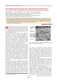
from the cross-sectional transmission electron microscope<br />
(TEM) image.<br />
We observed remarkable enhancement of D<strong>UV</strong> emission<br />
of <strong>AlGaN</strong>-QWs by fabricating them on the highquality<br />
AlN template [19]. Figure 5 shows PL spectra of<br />
<strong>AlGaN</strong> QWs with peak emission wavelength at around<br />
254 <strong>nm</strong> <strong>fabricated</strong> on ML-AlN templates with various values<br />
of XRC (1012) FWHM. The 254 <strong>nm</strong> QWs were excited<br />
with 244 <strong>nm</strong> Ar-SHG laser. The excitation power<br />
Figure 5 PL spectra of <strong>AlGaN</strong> QWs with peak emission wavelength<br />
at around 254 <strong>nm</strong> <strong>fabricated</strong> on ML-AlN templates with<br />
various values of XRC (10 12) FWHM.<br />
density was approximately 200 W/cm 2 . As seen in Fig. 5,<br />
the emission intensity was significantly increased by improving<br />
the XRC (1012) FWHM. The PL intensity was increased<br />
by more than 50 times by reducing the XRC<br />
(1012) FWHM from 1400 arcsec to 500 arcsec. From<br />
Fig. 5, we found that PL intensity of the QW was rapidly<br />
increased when FWHM of XRC (1012) of <strong>AlGaN</strong> buffer is<br />
reduced to 500–800 arcsec. We obtained similar emission<br />
enhancement for the 260 <strong>nm</strong>, 270 <strong>nm</strong> <strong>and</strong> 280 <strong>nm</strong> b<strong>and</strong><br />
<strong>AlGaN</strong>-QWs.<br />
3 222–273 <strong>nm</strong> <strong>AlGaN</strong> QW <strong>LEDs</strong> <strong>fabricated</strong> on<br />
ML-AlN templates Figure 6 shows a schematic of the<br />
sample structure <strong>and</strong> emission image of an <strong>AlGaN</strong> MQW<br />
D<strong>UV</strong> LED <strong>fabricated</strong> on a ML-AlN template. Table 1<br />
shows the typical designed values of Al compositions x in<br />
Al x Ga 1–x N wells, buffer <strong>and</strong> barrier layers, <strong>and</strong> electronblocking<br />
layers (EBLs) used for 222–273 <strong>nm</strong> <strong>AlGaN</strong>-<br />
MQW <strong>LEDs</strong>. High Al content <strong>AlGaN</strong> layers were used in<br />
order to obtain short wavelength <strong>UV</strong> emissions, as shown<br />
in Table 1. Figure 7 shows a cross-sectional TEM image of<br />
an <strong>AlGaN</strong> MQW D<strong>UV</strong> LED with emission wavelength at<br />
227 <strong>nm</strong> <strong>fabricated</strong> on a ML-AlN template. We grew an approximately<br />
1 μm thick Si-doped Al 0.87 Ga 0.13 N buffer-layer,<br />
followed by a 3-layer MQW region consisting of 1.3 <strong>nm</strong><br />
thick Al 0.79 Ga 0.21 N wells <strong>and</strong> 7 <strong>nm</strong> thick Al 0.87 Ga 0.13 N barriers,<br />
a 21 <strong>nm</strong> thick undoped Al 0.87 Ga 0.13 N barrier, a 15 <strong>nm</strong><br />
thick Mg-doped Al 0.98 Ga 0.02 N electron-blocking layer<br />
(EBL), a 10 <strong>nm</strong> thick Mg-doped Al 0.87 Ga 0.13 N p-layer <strong>and</strong><br />
an approximately 20 <strong>nm</strong> thick Mg-doped GaN contact<br />
layer on the ML-AlN buffer. The quantum well thickness<br />
was changed within the range of 1.3–2 <strong>nm</strong>. We used a thin<br />
quantum well in order to obtain a high IQE by suppressing<br />
the effects of the polarization field in the well. It is believed<br />
to be particularly important to obtain atomically<br />
smooth hetero-interfaces to obtain a high IQE from such a<br />
thin QW, because the quantized energy level broadening<br />
© 2009 WILEY-VCH Verlag GmbH & Co. KGaA, Weinheim www.pss-a.com<br />
-131-
Original<br />
Paper<br />
Phys. Status Solidi A 206, No. 6 (2009) 1179<br />
Ni/Au Electrode<br />
Ni/Au<br />
ML-AlN Buffer<br />
(NH 3 Pulse-Flow Method)<br />
Sapphire Sub.<br />
GaN;Mg<br />
Al 0.87Ga 0.13N;Mg<br />
Al 0.98Ga 0.02N;Mg<br />
E-Blocking Layer<br />
Al 0.79Ga 0.21N/<br />
Al 0.87Ga 0.13N<br />
3-layer MQW<br />
n-Al 0.87Ga 0.13N;Si<br />
<strong>UV</strong> Output<br />
Figure 7 Cross-sectional TEM image of an <strong>AlGaN</strong> MQW D<strong>UV</strong><br />
LED with emission wavelength of 227 <strong>nm</strong>.<br />
Figure 6 (online colour at: www.pss-a.com) Schematic sample<br />
structure <strong>and</strong> emission images of an <strong>AlGaN</strong> MQW D<strong>UV</strong> LED<br />
with emission wavelength at 227 <strong>nm</strong> <strong>fabricated</strong> on a ML-AlN<br />
buffer.<br />
due to the roughened hetero-interfaces would cause the<br />
reduction of emission intensity. The atomically flat heterointerfaces<br />
for the 1.3 <strong>nm</strong> thick three-layer QWs are confirmed<br />
by the cross-sectional TEM image, as seen in<br />
Fig. 7. Ni/Au electrodes were used for both n-type <strong>and</strong><br />
p-type electrodes. The size of the p-type electrode was<br />
300 × 300 µm. The output power radiated into the back of<br />
the LED was measured using a Si photodetector located<br />
behind the LED sample, which was calibrated to measure<br />
luminous flux from LED sources using an integrated-<br />
Table 1 Typical designed values of Al compositions x in<br />
Al x Ga 1–x N wells, buffer <strong>and</strong> barrier layers, <strong>and</strong> electron-blocking<br />
layers (EBLs) used for 222–273 <strong>nm</strong> <strong>AlGaN</strong>-MQW <strong>LEDs</strong>.<br />
wavelength well barrier & buffer electron blocking layer<br />
222 <strong>nm</strong> 0.83 0.89 0.98<br />
227 <strong>nm</strong> 0.79 0.87 0.98<br />
234 <strong>nm</strong> 0.74 0.84 0.97<br />
248 <strong>nm</strong> 0.64 0.78 0.96<br />
255 <strong>nm</strong> 0.60 0.75 0.95<br />
261 <strong>nm</strong> 0.55 0.72 0.94<br />
273 <strong>nm</strong> 0.47 0.67 0.93<br />
spheres system. The <strong>LEDs</strong> were measured under bare wafer<br />
condition.<br />
Figure 8 shows electroluminescence (EL) spectra of<br />
the <strong>fabricated</strong> <strong>AlGaN</strong>-MQW <strong>LEDs</strong> with wavelengths of<br />
222, 227, 234, 248, 255 <strong>and</strong> 261 <strong>nm</strong>, <strong>and</strong> quaternary<br />
In<strong>AlGaN</strong>-MQW <strong>LEDs</strong> with wavelengths of 282 <strong>nm</strong>, all<br />
measured at room temperature (RT) with injection current<br />
of around 50 mA. The pulse width <strong>and</strong> repetition<br />
frequency used for the pulsed current injection were 10 μs<br />
<strong>and</strong> 10 kHz, respectively. As can be seen in Fig. 8, singlepeaked<br />
operations were obtained for every sample. The<br />
222 <strong>nm</strong> is the shortest wavelength to date for an<br />
<strong>AlGaN</strong>-<strong>based</strong> LED on sapphire.<br />
Normalized Intensity<br />
<strong>AlGaN</strong> QW<br />
D<strong>UV</strong> <strong>LEDs</strong><br />
222<strong>nm</strong> Pulsed<br />
227<strong>nm</strong> Pulsed<br />
234<strong>nm</strong> CW<br />
248<strong>nm</strong> CW<br />
255<strong>nm</strong> CW<br />
261<strong>nm</strong> CW<br />
In<strong>AlGaN</strong> QW<br />
D<strong>UV</strong> LED<br />
282<strong>nm</strong> CW<br />
Measured at RT<br />
200 250 300 350 400<br />
Wavelength (<strong>nm</strong>)<br />
Figure 8 (online colour at: www.pss-a.com) EL spectra of the<br />
<strong>fabricated</strong> <strong>AlGaN</strong>-MQW <strong>LEDs</strong> with wavelengths of 222, 227,<br />
234, 248, 255 <strong>and</strong> 261 <strong>nm</strong>, <strong>and</strong> quaternary In<strong>AlGaN</strong>-MQW <strong>LEDs</strong><br />
with wavelengths of 282 <strong>nm</strong>, all measured at RT with injection<br />
current of around 50 mA.<br />
www.pss-a.com<br />
© 2009 WILEY-VCH Verlag GmbH & Co. KGaA, Weinheim<br />
-132-
physica<br />
pss<br />
status<br />
solidi<br />
a<br />
1180 H. Hirayama et al.: <strong>222–282</strong> <strong>nm</strong> <strong>AlGaN</strong> <strong>and</strong> In<strong>AlGaN</strong>-<strong>based</strong> <strong>deep</strong>-<strong>UV</strong> <strong>LEDs</strong><br />
Output Power (mW)<br />
2<br />
DE EBL=420meV<br />
l=250<strong>nm</strong><br />
(a)<br />
DE EBL=280meV<br />
Dl=254<strong>nm</strong><br />
1<br />
RT CW<br />
<strong>AlGaN</strong>-3MQW<br />
D<strong>UV</strong>-LED<br />
on ML-AlN<br />
0<br />
0 100 200 300 400<br />
Current (mA)<br />
EQE η ext (%)<br />
0.5<br />
0.4<br />
0.3<br />
0.2<br />
0.1<br />
DE EBL=420meV<br />
l=250<strong>nm</strong><br />
DE EBL=280meV<br />
l=254<strong>nm</strong><br />
(b)<br />
RT CW<br />
0<br />
0 100 200 300 400<br />
Current (mA)<br />
Figure 9 (online colour at: www.pss-a.com) (a) I–L <strong>and</strong> (b)<br />
I-EQE characteristics for two types 250 <strong>nm</strong> b<strong>and</strong> <strong>AlGaN</strong>-MQW<br />
<strong>LEDs</strong> under RT CW operation.<br />
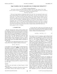
Figure 9 shows (a) current vs. output power (I–L) <strong>and</strong><br />
(b) current vs. EQE η ext characteristics for two types<br />
250 <strong>nm</strong> b<strong>and</strong> <strong>AlGaN</strong>-MQW <strong>LEDs</strong> under RT CW operation.<br />
The electron barrier height of EBL <strong>and</strong> the peak wavelength<br />
of the two types <strong>LEDs</strong> were 420 meV, 250 <strong>nm</strong> <strong>and</strong><br />
280 meV <strong>and</strong> 254 <strong>nm</strong>, respectively. As seen in Fig. 9(b),<br />
the EQE of the LED was significantly increased by using<br />
higher electron blocking height. This fact indicates that the<br />
electron injection efficiency (EIE) into the QW is markedly<br />
increased by the suppression of electron overflow.<br />
The maximum output power <strong>and</strong> EQE were 2.2 mW <strong>and</strong><br />
0.43%, respectively, for the LED with wavelength of<br />
250 <strong>nm</strong> under RT CW operation.<br />
We also obtained single-peaked EL spectra for sub-<br />
230 <strong>nm</strong> wavelength <strong>LEDs</strong>. The <strong>deep</strong>-level emissions were<br />
more then two orders of magnitude smaller than the main<br />
peak for the sub-230 <strong>nm</strong> wavelength <strong>LEDs</strong>. The output<br />
power of the 227 <strong>nm</strong> LED was 0.15 mW with injection<br />
current of 30 mA <strong>and</strong> the maximum EQE was 0.2%, under<br />
RT pulsed operation. We also obtained the maximum output<br />
power of 0.014 mW <strong>and</strong> EQE of 0.003% for 222 <strong>nm</strong><br />
<strong>AlGaN</strong> LED.<br />
4 Over 10 mW CW power 280 <strong>nm</strong> b<strong>and</strong><br />
In<strong>AlGaN</strong>-<strong>based</strong> D<strong>UV</strong>-LED Quaternary In<strong>AlGaN</strong> alloy is<br />
attracting much attention as c<strong>and</strong>idate material for realizing<br />
D<strong>UV</strong>-<strong>LEDs</strong>, since efficient <strong>UV</strong> emission as well as<br />
higher hole concentration can be obtained due to Inincorporation<br />
effects [16–18]. Figure 10 shows a schematic<br />
layer structure <strong>and</strong> a cross-sectional TEM image of a<br />
282 <strong>nm</strong> In<strong>AlGaN</strong>-<strong>based</strong> <strong>UV</strong>-LED. On the ML-AlN/sapphire<br />
template, we grew an approximately 2 μm thick<br />
Si-doped <strong>AlGaN</strong> buffer layer, a 3 <strong>nm</strong> thick undoped<br />
In<strong>AlGaN</strong> interlayer, a 20 <strong>nm</strong> thick Si-doped In<strong>AlGaN</strong><br />
buffer layer, a 2-layer MQW emitting region consisting<br />
of 1.7 <strong>nm</strong> thick undoped wells <strong>and</strong> 7 <strong>nm</strong> thick Si-doped<br />
In<strong>AlGaN</strong> barriers, a 10 <strong>nm</strong> thick undoped In<strong>AlGaN</strong> cap, a<br />
7 <strong>nm</strong> thick Mg-doped In<strong>AlGaN</strong> electron blocking layer<br />
(EBL), an approximately 50 <strong>nm</strong> thick Mg-doped In<strong>AlGaN</strong><br />
p-InGaN Contact<br />
p-In<strong>AlGaN</strong><br />
n-<strong>AlGaN</strong><br />
AlN(NH3 pulse-flow<br />
multi-layer growth)<br />
Sapphire(0001)<br />
p-In<strong>AlGaN</strong><br />
E-Block Layer (7<strong>nm</strong>)<br />
In<strong>AlGaN</strong> Cap (10<strong>nm</strong>)<br />
In<strong>AlGaN</strong> well<br />
(1.7<strong>nm</strong>)<br />
/In<strong>AlGaN</strong>:Si Barrier<br />
(7<strong>nm</strong>) 2QW<br />
In<strong>AlGaN</strong>:Si (20<strong>nm</strong>)<br />
i-In<strong>AlGaN</strong> Interlayer<br />
(3<strong>nm</strong>)<br />
Figure 10 (online colour at: www.pss-a.com) Schematic layer<br />
structure <strong>and</strong> a cross-sectional TEM image of a 282 <strong>nm</strong> InAl-<br />
GaN-<strong>based</strong> <strong>UV</strong>-LED.<br />
<strong>and</strong> a Mg-doped InGaN contact layer. The Al compositions<br />
of the In<strong>AlGaN</strong> used for well <strong>and</strong> barrier layer were approximately<br />
35% <strong>and</strong> 60%, respectively, in order to obtain<br />
a 280 <strong>nm</strong> b<strong>and</strong> emission from the QW. The In composition<br />
of the In<strong>AlGaN</strong> layers was estimated to be below 1%. The<br />
Al content used for In<strong>AlGaN</strong> EBL estimated by the growth<br />
condition was more than 90%.<br />
We achieved high-quality quaternary In<strong>AlGaN</strong> layers<br />
with high Al content (>45%) by using quite low growth<br />
rate, i.e., 0.03 μm/hour. The emission intensity of a 280 <strong>nm</strong><br />
b<strong>and</strong> quaternary In<strong>AlGaN</strong> QW at RT was increased by<br />
5 times by reducing the growth rate from 0.12 μm/hour to<br />
0.03 μm/hour. We introduced Si-doped In<strong>AlGaN</strong> buffer<br />
<strong>and</strong> barrier layers <strong>and</strong> undoped In<strong>AlGaN</strong> interlayer, for the<br />
purpose of obtaining atomically flat hetero-interfaces of<br />
the In<strong>AlGaN</strong> layers <strong>and</strong> reducing Piezoelectric field in the<br />
QWs. The Si concentration of the In<strong>AlGaN</strong> barrier layer<br />
was approximately 1 × 10 17 cm –3 . We confirmed that the<br />
surface roughness of In<strong>AlGaN</strong> layer was significantly improved<br />
by introducing Si-doped In<strong>AlGaN</strong> buffer layer. The<br />
PL intensity of In<strong>AlGaN</strong>-QW with Si-doped In<strong>AlGaN</strong> barrier<br />
was about 2 times higher than that with undoped<br />
Figure 11 (online colour at: www.pss-a.com) Wavelength dependence<br />
of the ratio of integrated PL intensity (PL at RT/PL at<br />
low temperature).<br />
10<strong>nm</strong><br />
© 2009 WILEY-VCH Verlag GmbH & Co. KGaA, Weinheim www.pss-a.com<br />
-133-
Original<br />
Paper<br />
Phys. Status Solidi A 206, No. 6 (2009) 1181<br />
Output Power (mW)<br />
10<br />
l=282<strong>nm</strong><br />
1.5<br />
5<br />
RT CW 0.5<br />
In<strong>AlGaN</strong>-2QW-LED<br />
on AlN/<strong>AlGaN</strong><br />
/Sapphire Sub.<br />
0<br />
0<br />
0 100 200 300<br />
Current (mA)<br />
1<br />
External Quantum Efficiency (%)<br />
Figure 12 Current vs. output power (I–L) <strong>and</strong> EQE characteristics<br />
of the 282 <strong>nm</strong> In<strong>AlGaN</strong> QW <strong>UV</strong>-LED with Si-doped<br />
In<strong>AlGaN</strong> layers.<br />
In<strong>AlGaN</strong> barrier. We also obtained marked emission enhancement<br />
of QWs by inserting Si-doped In<strong>AlGaN</strong> buffer<br />
layer <strong>and</strong> i-In<strong>AlGaN</strong> interlayer.<br />
Figure 11 summarizes the wavelength dependence of<br />
the ratio of integrated PL intensity (PL at RT/PL at low<br />
temperature). We usually measure the low temperature PL<br />
at 10 K. As shown in Fig. 11, an <strong>AlGaN</strong> D<strong>UV</strong> emission<br />
at RT is weak when we use high TDD AlN template<br />
(TDD > 2 × 10 10 cm –2 ). We achieved high-efficiency emission<br />
both for <strong>AlGaN</strong> <strong>and</strong> In<strong>AlGaN</strong> QWs, by fabricating<br />
them on low TDD ML-AlN template. The maximum ratios<br />
of the integrated PL intensity were 30% <strong>and</strong> 86% for<br />
280 <strong>nm</strong> b<strong>and</strong> <strong>AlGaN</strong> <strong>and</strong> In<strong>AlGaN</strong> QWs, respectively.<br />
This result suggests that extremely high IQE can be obtained<br />
from the In<strong>AlGaN</strong>-QW at RT by fabricating them<br />
on a low TDD AlN buffer.<br />
Figure 12 shows current vs. output power (I–L) <strong>and</strong><br />
EQE characteristics of the In<strong>AlGaN</strong> QW <strong>UV</strong>-LED with<br />
Si-doped <strong>and</strong> Mg-doped In<strong>AlGaN</strong> layers. Single peaked<br />
EL was obtained with the wavelength at 282 <strong>nm</strong>. The<br />
maximum output power <strong>and</strong> EQE were 10.6 mW <strong>and</strong><br />
1.2%, respectively, under RT CW operation. From these<br />
results, we found that quaternary In<strong>AlGaN</strong> QW <strong>and</strong> p-type<br />
In<strong>AlGaN</strong> is quite useful for achieving high-efficiency<br />
D<strong>UV</strong>-<strong>LEDs</strong>. We also found the control of n-type doping<br />
layer around the In<strong>AlGaN</strong>-<strong>based</strong> QW was effective for obtaining<br />
high-efficiency D<strong>UV</strong>-<strong>LEDs</strong>.<br />
Figure 13 summarizes maximum output power of<br />
<strong>AlGaN</strong> <strong>and</strong> In<strong>AlGaN</strong> <strong>based</strong> D<strong>UV</strong>-<strong>LEDs</strong> for the various<br />
development stages of our group. When the TDD of the<br />
AlN template was higher than 2 × 10 10 cm –2 , the emission<br />
from the <strong>UV</strong>-LED was weak <strong>and</strong> not single-peak. We obtained<br />
single-peaked 240–260 <strong>nm</strong> b<strong>and</strong> <strong>LEDs</strong> by reducing<br />
edge-type TDD to 3.2 × 10 9 cm –2 , as described in the<br />
Ref. [9] in 2007. A significant increase of CW output<br />
power was observed by reducing the TDD, as shown in<br />
Fig. 13. We also found that the higher electron blocking<br />
height is effective for obtaining high output power. The<br />
Max. Output Power (mW)<br />
10 2<br />
10<br />
1<br />
10 -1<br />
10 -2<br />
10 -3<br />
10 -4<br />
10 -5<br />
TDD(Edge)2×10 10 cm -2<br />
Emission is weak <strong>and</strong> not<br />
single peak.<br />
200 220 240 260 280 300<br />
Wavelength (<strong>nm</strong>)<br />
Figure 13 (online colour at: www.pss-a.com) Maximum output<br />
power of <strong>AlGaN</strong> <strong>and</strong> In<strong>AlGaN</strong> <strong>based</strong> D<strong>UV</strong>-<strong>LEDs</strong> for the various<br />
development stages of our group.<br />
output power of the 250 <strong>nm</strong> b<strong>and</strong> LED was increased<br />
by more than 30 times by reducing the TDD from<br />
3.2 × 10 9 cm –2 to 7.5 × 10 8 cm –2 . We also used DOWA<br />
Electronics Ltd. Corporation’s AlN/sapphire templates<br />
with XRC (10 12) FWHM of 250–350 arcsec, in order to<br />
obtain higher output power of <strong>AlGaN</strong> <strong>LEDs</strong>. We obtained<br />
over 1 mW CW output power for 241–282 <strong>nm</strong> D<strong>UV</strong>-<br />
<strong>LEDs</strong>. The maximum output power of the 241 <strong>nm</strong> <strong>and</strong><br />
256 <strong>nm</strong> <strong>LEDs</strong> were 1.1 mW <strong>and</strong> 4.0 mW, respectively, under<br />
RT CW operations. We obtained over 10 mW CW<br />
power with wavelength of 280 <strong>nm</strong>, which is available for<br />
sterilization application.<br />
Figure 14 summarizes the EQE of 200–300 <strong>nm</strong> b<strong>and</strong><br />
III-nitride D<strong>UV</strong>-<strong>LEDs</strong> obtained by our group. The EQE<br />
observed for the 220 <strong>nm</strong> b<strong>and</strong> <strong>AlGaN</strong> LED were extremely<br />
high compared with those for the 210 <strong>nm</strong> LED using AlN<br />
emitting layer [14]. The reason of obtaining higher efficiency<br />
for the <strong>AlGaN</strong> LED compared with AlN LED is<br />
EQE η ext (%)<br />
10 2<br />
10 1<br />
282<strong>nm</strong><br />
250<strong>nm</strong> 264<strong>nm</strong> 1.2% (CW)<br />
0.43% 0.6%(CW)<br />
10 0 227<strong>nm</strong> 0.2% (CW)<br />
(Pulsed)<br />
10 -1 222<strong>nm</strong><br />
In<strong>AlGaN</strong>-QW<br />
0.003%<br />
LED<br />
(Pulsed)<br />
10 -2<br />
10 -3<br />
<strong>AlGaN</strong>-QW<br />
10 -4<br />
<strong>LEDs</strong><br />
NTT<br />
10 -5 AlN-LED<br />
210<strong>nm</strong>, 10 -6 %<br />
10 -6<br />
200 220 240 260 280 300<br />
Wavelength (<strong>nm</strong>)<br />
Wavelength for<br />
Sterilization<br />
Figure 14 (online colour at: www.pss-a.com) EQE of 200–<br />
300 <strong>nm</strong> b<strong>and</strong> <strong>AlGaN</strong> <strong>and</strong> In<strong>AlGaN</strong> <strong>based</strong> D<strong>UV</strong>-<strong>LEDs</strong> achieved<br />
by our group.<br />
www.pss-a.com<br />
© 2009 WILEY-VCH Verlag GmbH & Co. KGaA, Weinheim<br />
-134-
physica<br />
pss<br />
status<br />
solidi<br />
a<br />
1182 H. Hirayama et al.: <strong>222–282</strong> <strong>nm</strong> <strong>AlGaN</strong> <strong>and</strong> In<strong>AlGaN</strong>-<strong>based</strong> <strong>deep</strong>-<strong>UV</strong> <strong>LEDs</strong><br />
that a sufficient electron–hole confinement into QWs <strong>and</strong><br />
an efficient carrier injection can be obtained by utilizing an<br />
<strong>AlGaN</strong>-<strong>based</strong> heterostructure. The maximum EQE of sub-<br />
300 <strong>nm</strong> LED obtained by our group was 1.2%. One of the<br />
reasons of low EQE for sub-300 <strong>nm</strong> nitride <strong>LEDs</strong> is considered<br />
to be low light extraction efficiency (