Xilinx XC4000E and XC4000X Series FPGA data sheet functional ...
Xilinx XC4000E and XC4000X Series FPGA data sheet functional ...
Xilinx XC4000E and XC4000X Series FPGA data sheet functional ...

You also want an ePaper? Increase the reach of your titles
YUMPU automatically turns print PDFs into web optimized ePapers that Google loves.
R<br />
<strong>XC4000E</strong> <strong>and</strong> <strong>XC4000X</strong> <strong>Series</strong> Field Programmable Gate Arrays<br />
circuit prevents undefined floating levels. However, it is<br />
overridden by any driver, even a pull-up resistor.<br />
Each <strong>XC4000E</strong> longline has a programmable splitter switch<br />
at its center, as does each <strong>XC4000X</strong> longline driven by<br />
TBUFs. This switch can separate the line into two independent<br />
routing channels, each running half the width or height<br />
of the array.<br />
Each <strong>XC4000X</strong> longline not driven by TBUFs has a buffered<br />
programmable splitter switch at the 1/4, 1/2, <strong>and</strong> 3/4<br />
points of the array. Due to the buffering, <strong>XC4000X</strong> longline<br />
performance does not deteriorate with the larger array<br />
sizes. If the longline is split, the resulting partial longlines<br />
are independent.<br />
Routing connectivity of the longlines is shown in Figure 27<br />
on page 30.<br />
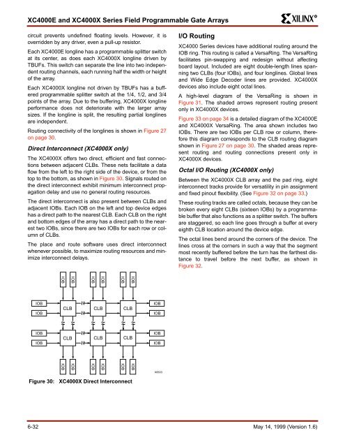
Direct Interconnect (<strong>XC4000X</strong> only)<br />
The <strong>XC4000X</strong> offers two direct, efficient <strong>and</strong> fast connections<br />
between adjacent CLBs. These nets facilitate a <strong>data</strong><br />
flow from the left to the right side of the device, or from the<br />
top to the bottom, as shown in Figure 30. Signals routed on<br />
the direct interconnect exhibit minimum interconnect propagation<br />
delay <strong>and</strong> use no general routing resources.<br />
The direct interconnect is also present between CLBs <strong>and</strong><br />
adjacent IOBs. Each IOB on the left <strong>and</strong> top device edges<br />
has a direct path to the nearest CLB. Each CLB on the right<br />
<strong>and</strong> bottom edges of the array has a direct path to the nearest<br />
two IOBs, since there are two IOBs for each row or column<br />
of CLBs.<br />
The place <strong>and</strong> route software uses direct interconnect<br />
whenever possible, to maximize routing resources <strong>and</strong> minimize<br />
interconnect delays.<br />
I/O Routing<br />
XC4000 <strong>Series</strong> devices have additional routing around the<br />
IOB ring. This routing is called a VersaRing. The VersaRing<br />
facilitates pin-swapping <strong>and</strong> redesign without affecting<br />
board layout. Included are eight double-length lines spanning<br />
two CLBs (four IOBs), <strong>and</strong> four longlines. Global lines<br />
<strong>and</strong> Wide Edge Decoder lines are provided. <strong>XC4000X</strong><br />
devices also include eight octal lines.<br />
A high-level diagram of the VersaRing is shown in<br />
Figure 31. The shaded arrows represent routing present<br />
only in <strong>XC4000X</strong> devices.<br />
Figure 33 on page 34 is a detailed diagram of the <strong>XC4000E</strong><br />
<strong>and</strong> <strong>XC4000X</strong> VersaRing. The area shown includes two<br />
IOBs. There are two IOBs per CLB row or column, therefore<br />
this diagram corresponds to the CLB routing diagram<br />
shown in Figure 27 on page 30. The shaded areas represent<br />
routing <strong>and</strong> routing connections present only in<br />
<strong>XC4000X</strong> devices.<br />
Octal I/O Routing (<strong>XC4000X</strong> only)<br />
Between the <strong>XC4000X</strong> CLB array <strong>and</strong> the pad ring, eight<br />
interconnect tracks provide for versatility in pin assignment<br />
<strong>and</strong> fixed pinout flexibility. (See Figure 32 on page 33.)<br />
These routing tracks are called octals, because they can be<br />
broken every eight CLBs (sixteen IOBs) by a programmable<br />
buffer that also functions as a splitter switch. The buffers<br />
are staggered, so each line goes through a buffer at every<br />
eighth CLB location around the device edge.<br />
The octal lines bend around the corners of the device. The<br />
lines cross at the corners in such a way that the segment<br />
most recently buffered before the turn has the farthest distance<br />
to travel before the next buffer, as shown in<br />
Figure 32.<br />
IOB<br />
IOB<br />
IOB<br />
IOB<br />
IOB<br />
IOB<br />
IOB<br />
IOB<br />
IOB<br />
IOB<br />
CLB<br />
~ ~<br />
CLB<br />
~ ~ ~ ~<br />
CLB<br />
~ ~<br />
CLB<br />
CLB<br />
~ ~<br />
CLB<br />
IOB<br />
IOB<br />
IOB<br />
IOB<br />
IOB<br />
IOB<br />
IOB<br />
IOB<br />
IOB<br />
IOB<br />
X6603<br />
Figure 30: <strong>XC4000X</strong> Direct Interconnect<br />
6-32 May 14, 1999 (Version 1.6)