FAS466 Fast Architecture SCSI Processor
FAS466 Fast Architecture SCSI Processor
FAS466 Fast Architecture SCSI Processor

Create successful ePaper yourself
Turn your PDF publications into a flip-book with our unique Google optimized e-Paper software.
QLogic Corporation<br />
<strong>FAS466</strong> <strong>Fast</strong> <strong>Architecture</strong> <strong>SCSI</strong> <strong>Processor</strong><br />
Data Sheet<br />
Features Summary<br />
■<br />
■<br />
■<br />
■<br />
■<br />
■<br />
■<br />
■<br />
■<br />
Compliance with ANSI X3T10/855D <strong>SCSI</strong><br />
configured automatically (SCAM) protocol levels 1<br />
and 2<br />
Compliance with ANSI X3.131-1996 <strong>SCSI</strong>-3<br />
parallel interface (SPI-2) standard<br />
Compliance with ANSI X3T10/1142D <strong>Fast</strong>-40<br />
standard<br />
<strong>SCSI</strong> synchronous data transfer rates up to:<br />
❒ 80 Mbytes/sec (wide, 16-bit <strong>Fast</strong>-40)<br />
❒ 40 Mbytes/sec (narrow, eight-bit <strong>Fast</strong>-40)<br />
On-chip LVD (low voltage differential) drivers<br />
Versatile 40 million instructions per second (MIP)<br />
microcontroller<br />
Programmable microcontroller to automate <strong>SCSI</strong><br />
protocol handling<br />
Programmable filtering on select <strong>SCSI</strong> signals<br />
Programmable slew-rate control<br />
■ Supports initiator and target modes<br />
■ DMA interface with late transfer tolerant design<br />
that provides 160 Mbytes/sec sustained transfers<br />
■ Expanded 128-word DMA FIFO<br />
■ On-chip phase lock loop (PLL) for high frequency<br />
clock synthesis<br />
Product Description<br />
The <strong>FAS466</strong> incorporates an enhanced,<br />
high-performance <strong>SCSI</strong> engine derived from the QLogic<br />
TEC450/452 triple embedded controller family.<br />
The <strong>FAS466</strong> provides <strong>Fast</strong>-40 <strong>SCSI</strong> synchronous<br />
transfer rates. The highly integrated <strong>SCSI</strong> core provides<br />
advanced SCAM level 1 and level 2 support. The <strong>FAS466</strong><br />
includes a microcontroller that provides a flexible,<br />
programmable means to coordinate <strong>SCSI</strong> sequences.<br />
The <strong>FAS466</strong> supports single-ended and low-voltage<br />
differential <strong>SCSI</strong> mode operations in initiator and target<br />
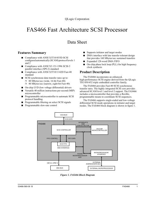
modes. The <strong>FAS466</strong> block diagram is shown in figure 1.<br />
<strong>SCSI</strong> BUS<br />
<strong>SCSI</strong> DATA<br />
<strong>FAS466</strong><br />
INTERRUPTS<br />
AND<br />
STATUS VECTOR<br />
<strong>SCSI</strong> CONTROLLER<br />
ON-CHIP<br />
MICROCONTROLLER<br />
FIFO CONTROL<br />
FIFO DATA<br />
<strong>SCSI</strong> FIFO<br />
DMA INTERFACE<br />
<strong>FAS466</strong><br />
MICROPROCESSOR<br />
BUS<br />
MICROPROCESSOR<br />
INTERFACE<br />
DB15-0, DPB1-0<br />
DMA BUS<br />
EXTERNAL<br />
ADDRESS/DATA BUS<br />
EXTERNAL MICROPROCESSOR<br />
Figure 1. <strong>FAS466</strong> Block Diagram<br />
53466-580-00 B <strong>FAS466</strong> 1
QLogic Corporation<br />
<strong>SCSI</strong> Controller<br />
The following list highlights the <strong>FAS466</strong> <strong>SCSI</strong><br />
controller features.<br />
■ Asynchronous data transfers greater than<br />
5 Mtransfers/sec<br />
■ Synchronous data transfers (5 Mtransfers/sec)<br />
■ <strong>Fast</strong> synchronous data transfers (10 Mtransfers/sec)<br />
■ <strong>Fast</strong>-20 synchronous data transfers<br />
(20 Mtransfers/sec)<br />
■ <strong>Fast</strong>-40 synchronous data transfers<br />
(40 Mtransfers/sec)<br />
■ 8-bit (narrow) and 16-bit (wide) <strong>SCSI</strong> bus widths<br />
■ SCAM levels 1 and 2<br />
The <strong>SCSI</strong> controller provides powerful and flexible<br />
low-level hardware assistance for <strong>SCSI</strong> protocol handling.<br />
The <strong>FAS466</strong> microcontroller, <strong>SCSI</strong> FIFO, and <strong>SCSI</strong><br />
controller perform frequently used <strong>SCSI</strong> operations with<br />
low firmware overhead at performance levels ranging from<br />
asynchronous <strong>SCSI</strong> to <strong>Fast</strong>-40.<br />
The core of the <strong>FAS466</strong> <strong>SCSI</strong> processor, with enhanced<br />
initiator support, is derived from the proven TEC452 <strong>SCSI</strong><br />
disk controller.<br />
Microcontroller<br />
The following list highlights the <strong>FAS466</strong> <strong>SCSI</strong><br />
microcontroller features.<br />
■ Maximum 40 MIPS with a 25-ns instruction cycle<br />
(except for branch)<br />
■ 64 single-word instructions<br />
■ 16-bit wide instructions<br />
■ Eight-bit wide data path<br />
■ 1024x16 static random access memory (SRAM)<br />
program memory<br />
■ 16x8 dual-port, general purpose registers;<br />
32 mailbox registers<br />
■ Five-level deep hardware stack<br />
■ Direct, indirect, and absolute addressing modes<br />
■ Two firmware interrupt sources<br />
■ Two hardware interrupts; one with four-bit,<br />
automatic interrupt vector and status<br />
■ Full chip access through the microprocessor bus<br />
The <strong>FAS466</strong> provides a microcontroller with separate<br />
program and data memory. The result is improved<br />
bandwidth over traditional Von Neuman architecture where<br />
program and data share the same memory. Separating<br />
program and data memory allows independent widths for<br />
instruction and data. All instructions are 16 bit wide,<br />
single-word.<br />
The four operations for each instruction cycle are fetch,<br />
decode, execute, and write back. A three-stage pipeline<br />
allows overlaps between fetch and write-back cycles with<br />
decode and execute cycles. Consequently, all instructions<br />
execute in one instruction cycle or two clock periods (25 ns<br />
at 80 MHz) except for program branches, which require<br />
two instruction cycles.<br />
The microcontroller is composed of a 1024x16<br />
program memory, a 32x8 register file, a 5x8 stack, an<br />
integer ALU, 32 mailbox registers, and other special<br />
purpose registers. The microcontroller has direct access to<br />
addresses in the register files or in data memory. The first<br />
16 bytes of the external <strong>SCSI</strong> FIFO is mapped directly into<br />
data memory locations 90h-9Fh. The microcontroller can<br />
monitor the FIFO contents (one byte at a time) without<br />
removing it. The microcontroller accesses external<br />
registers through the external access read (EARD)<br />
instruction or the external access write (EAWR)<br />
instruction.<br />
DMA Interface<br />
The <strong>FAS466</strong> has an improved DMA interface with an<br />
expanded 128-word FIFO that provides transfer rates up to<br />
160 Mbytes/sec. The <strong>FAS466</strong> supports 16-bit wide data<br />
strobe transfers of up to 80 MHz with 160 Mbytes/sec data<br />
throughput. The internal FIFO provides programmable<br />
threshold logic for determining FIFO full and empty<br />
conditions.<br />
Microprocessor Interface<br />
The <strong>FAS466</strong> microprocessor interface provides the<br />
interface between the internal modules (<strong>SCSI</strong> controller,<br />
FIFO, microcontroller, and DMA engine) and an external<br />
microprocessor.<br />
Interfaces<br />
The <strong>FAS466</strong> interfaces consist of <strong>SCSI</strong>,<br />
microprocessor, DMA, and differential mode support. Pins<br />
that support these interfaces and other chip operations are<br />
shown in figure 2.<br />
2 <strong>FAS466</strong> 53466-580-00 B
QLogic Corporation<br />
MICROPROCESSOR<br />
INTERFACE<br />
8<br />
AD7-0<br />
ALE<br />
ARDY<br />
CS<br />
GP1/ADRSEN<br />
INT<br />
<strong>FAS466</strong><br />
AF_AE<br />
DACK<br />
DBOE<br />
DB15-0 16<br />
DBP1-0<br />
DMACLK<br />
DREQ<br />
2<br />
DMA INTERFACE<br />
RD<br />
FF_FE<br />
14<br />
WR<br />
GP2/LB/DIF<br />
PAUSE<br />
27<br />
<strong>SCSI</strong> INTERFACE<br />
2<br />
2<br />
2<br />
ACK/ACK<br />
ATN/ATN<br />
BSY/BSY<br />
CLKSEL<br />
FILTER<br />
MISCELLANEOUS<br />
2<br />
2<br />
2<br />
CD/CD<br />
DIFFSENS<br />
IO/IO<br />
LVDREF<br />
MSG/MSG<br />
GP0/TEST<br />
RESET<br />
TESTCLK<br />
VCOCLK<br />
6<br />
56<br />
2<br />
4<br />
2<br />
2<br />
32<br />
REQ/REQ<br />
RST/RST<br />
SD15-0/SD15-0<br />
SDP1-0/SDP1-0<br />
SEL/SEL<br />
144<br />
VDD<br />
VDD_PLO<br />
VDD5V<br />
VSS<br />
VSS_PLO<br />
16<br />
21<br />
2<br />
POWER AND<br />
GROUND<br />
41<br />
Figure 2. <strong>FAS466</strong> Functional Signal Grouping<br />
53466-580-00 B <strong>FAS466</strong> 3
QLogic Corporation<br />
Specifications are subject to change without notice.<br />
QLogic is a trademark of QLogic Corporation.<br />
©September 18, 1998 QLogic Corporation, 3545 Harbor Blvd., Costa Mesa, CA 92626, (800) ON-CHIP-1 or (714) 438-2200<br />
4 <strong>FAS466</strong> 53466-580-00 B