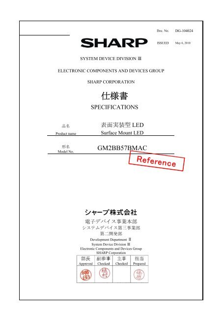
仕様書 - Sharp Corporation of Australia
仕様書 - Sharp Corporation of Australia
仕様書 - Sharp Corporation of Australia

You also want an ePaper? Increase the reach of your titles
YUMPU automatically turns print PDFs into web optimized ePapers that Google loves.
Doc. No.<br />
DG-104024<br />
ISSUED May 6, 2010<br />
SYSTEM DEVICE DIVISION Ⅲ<br />
ELECTRONIC COMPONENTS AND DEVICES GROUP<br />
SHARP CORPORATION<br />
仕 様 書<br />
SPECIFICATIONS<br />
品 名<br />
Product name<br />
表 面 実 装 型 LED<br />
Surface Mount LED<br />
形 名<br />
Model No.<br />
GM2BB57BMAC<br />
Reference<br />
電 子 デバイス 事 業 本 部<br />
システムデバイス 第 三 事 業 部<br />
第 二 開 発 部<br />
Development Department Ⅱ<br />
System Device Division Ⅲ<br />
Electronic Components and Devices Group<br />
SHARP <strong>Corporation</strong>
品 名 表 面 実 装 型 LED<br />
Product name<br />
形 名<br />
Model No.<br />
Reference<br />
Surface Mount LED<br />
GM2BB57BMAC<br />
Model No. GM2BB57BMAC<br />
Doc. No. DG-104024 Page 1/ 23<br />
○ 本 仕 様 書 は 弊 社 の 著 作 権 等 に 係 る 内 容 も 含 まれていますので、 取 り 扱 いには 充 分 ご 注 意 頂 くと 共 に、 本 仕 様 書 の 内 容 を 弊<br />
社 に 無 断 で 複 製 しないようお 願 い 申 し 上 げます。<br />
○ 本 製 品 のご 使 用 に 際 しては、 本 仕 様 書 に 記 載 された 使 用 条 件 及 び 以 下 の 注 意 事 項 を 遵 守 願 います。<br />
本 仕 様 書 記 載 の 使 用 条 件 あるいは 以 下 の 注 意 事 項 を 逸 脱 した 本 製 品 の 使 用 等 に 起 因 する 損 害 に 関 して、 弊 社 は 一 切 その 責<br />
を 負 いません。<br />
( 注 意 事 項 )<br />
1 お 客 様 が 本 仕 様 書 の 内 容 に 基 づき、お 客 様 の 商 品 のカタログ、 取 扱 い 説 明 書 等 を 作 成 される 場 合 には、 本 製 品 をお 客<br />
様 の 商 品 に 組 み 込 んだ 状 態 で、その 合 理 的 根 拠 の 有 無 をご 検 証 頂 きますようお 願 い 致 します。<br />
2 本 製 品 は 原 則 として 下 記 の 用 途 に 使 用 する 目 的 で 製 造 された 製 品 です。<br />
尚 、 下 記 の 用 途 であっても、3に 記 載 の 各 種 安 全 装 置 に 使 用 される 場 合 は3の 注 意 事 項 を 遵 守 願 います。<br />
又 、 下 記 の 用 途 であっても、それが4に 記 載 の 各 機 器 を 構 成 する 場 合 はご 使 用 にならないで 下 さい。<br />
・OA 機 器 ・ 計 測 器 ・ 工 作 機 器 ・AV 機 器<br />
・ 家 電 製 品 ・ 通 信 機 器 ( 幹 線 以 外 )<br />
3 特 に 高 い 信 頼 性 が 必 要 とされる 下 記 の 機 器 に 本 製 品 を 使 用 される 場 合 は、 必 ず 事 前 に 弊 社 販 売 窓 口 までご 連 絡 頂 くと<br />
共 に、これらのシステム・ 機 器 全 体 の 信 頼 性 および 安 全 性 維 持 のためにお 客 様 の 責 任 において 機 器 側 のフェールセー<br />
フ 設 計 や 冗 長 設 計 等 の 適 切 な 措 置 を 講 じて 頂 くようお 願 い 致 します。<br />
・ 運 送 機 器 ( 航 空 機 、 列 車 、 自 動 車 等 )の 制 御 または 各 種 安 全 性 にかかわるユニット<br />
・ 大 型 電 算 機 ・ 交 通 信 号 機 ・ガス 漏 れ 検 知 遮 断 機 ・ 防 災 防 犯 装 置<br />
・その 他 各 種 安 全 装 置 等 等<br />
4 機 能 ・ 精 度 等 において 極 めて 高 い 信 頼 性 が 要 求 される 以 下 の 機 器 にはご 使 用 にならないで 下 さい。<br />
・ 航 空 宇 宙 機 器 ・ 通 信 機 器 ( 幹 線 ) ・ 原 子 力 制 御 機 器<br />
・ 生 命 維 持 にかかわる 医 療 機 器 等<br />
5 上 記 1、2、3、4のいずれに 該 当 するか 疑 義 のある 場 合 は 弊 社 販 売 窓 口 までご 確 認 願 います。<br />
○ 本 製 品 につきご 不 明 な 点 がありましたら 事 前 に 弊 社 販 売 窓 口 までご 連 絡 頂 きますようお 願 い 致 します。<br />
○ Handle this document carefully for it contains material protected by international copyright law. Any reproduction, full or in part, <strong>of</strong> this material<br />
is prohibited without the express written permission <strong>of</strong> the company.<br />
○ When using the products covered herein, please observe the conditions written herein and the precautions outlined in the following paragraphs.<br />
In no event shall the company be liable for any damages resulting form failure to strictly adhere to these conditions and precautions.<br />
(Precautions)<br />
(1) Please do verify the validity <strong>of</strong> this part after assembling it in customer’s products, when customer wants to make catalogue and<br />
instruction manual based on the specification sheet <strong>of</strong> this part.<br />
(2)The products covered herein are designed and manufactured for the following application areas. When using the products covered herein<br />
for the equipment listed in paragraph (3), even for the following application areas, be sure to observe the precautions given in Paragraph<br />
(3). Never use the products for the equipment listed in Paragraph (4).<br />
* OA equipment * Instrumentation and measuring equipment * Machine tools<br />
* Audiovisual equipment * Home appliances<br />
* Communication equipment other than for trunk lines<br />
(3) These contemplating using the products covered herein for the following equipment which demands high reliability, should first contact<br />
a sales representative <strong>of</strong> the company and then accept responsibility for incorporating into the design fail-safe operation, redundancy, and<br />
other appropriate measures for ensuring reliability and safety <strong>of</strong> the equipment and the overall system.<br />
* Control and safety devices for airplanes, trains, automobiles, and other transportation equipment<br />
* Mainframe computers * Traffic control systems<br />
* Gas leak detectors and automatic cut<strong>of</strong>f devices * Rescue and security equipment<br />
* Other safety devices and safety equipment, etc.<br />
(4) Do not use the products covered herein for the following equipment which demands extremely high performance in terms <strong>of</strong><br />
functionality, reliability, or accuracy.<br />
* Aerospace equipment * Communications equipment for trunk lines<br />
* Control equipment for the nuclear power industry * Medical equipment related to life support, etc.<br />
(5) Please direct all queries and comments regarding the interpretation <strong>of</strong> the above four Paragraphs to a sales representative <strong>of</strong> the company.<br />
○ Please direct all queries regarding the products covered herein to a sales representative <strong>of</strong> the company.
Reference<br />
Model No. GM2BB57BMAC<br />
Doc. No. DG-104024 Page 2/ 23<br />
GM2BB57BMAC 仕 様 書<br />
GM2BB57BMAC Specification<br />
● 適 用 範 囲 Application<br />
本 仕 様 書 は、 発 光 材 料 に InGaN 青 色 LED チップ+ 緑 色 蛍 光 体 + 赤 色 蛍 光 体 を 使 用 した 白 色<br />
( 高 演 色 )LED、GM2BB57BMAC に 適 用 されます。<br />
主 な 用 途 : 照 明 用 光 源<br />
These specifications apply to light emitting diode Model No. GM2BB57BMAC.<br />
[White LED (High colorrendering) composed <strong>of</strong> InGaN blue LED chip and green and red phosphors]<br />
Main application : Illumination<br />
1 定 格 及 び 特 性 Ratings and characteristics ............................................................................ 3<br />
1.1 絶 対 最 大 定 格 Absolute maximum ratings........................................................................ 3<br />
1.2 電 気 的 及 び 光 学 的 特 性 Electro-optical characteristics.................................................... 4<br />
1.3 ランク 表 Rank table.......................................................................................................... 5<br />
1.4 低 減 曲 線 Derating Curve .................................................................................................. 7<br />
1.5 特 性 図 ( 標 準 値 ) Characteristics Diagram (TYP.) ........................................................ 8<br />
2 外 形 及 び 内 部 等 価 回 路 図 External dimensions and equivalent circuit.............................. 9<br />
3 信 頼 性 Reliability............................................................................................................... 10<br />
3.1 試 験 項 目 及 び 試 験 条 件 Test items and test conditions ................................................. 10<br />
3.2 故 障 判 定 基 準 Failure criteria......................................................................................... 12<br />
4 品 質 水 準 Quality level........................................................................................................... 13<br />
4.1 適 用 規 格 Applied standard ............................................................................................. 13<br />
4.2 抜 取 方 式 Sampling inspection........................................................................................ 13<br />
4.3 検 査 項 目 及 び 欠 点 判 定 基 準 Inspection items and defect criteria................................. 13<br />
5 補 足 事 項 Supplements........................................................................................................... 14<br />
5.1 テーピング Taping ......................................................................................................... 14<br />
5.2 ラベル(リール) Label (on reel) .............................................................................. 17<br />
5.3 包 装 Packing.................................................................................................................... 18<br />
5.4 環 境 負 荷 物 質 の 非 含 有 状 況 Information on environmental impact substances ........... 19<br />
6 使 用 上 の 注 意 Precautions .................................................................................................... 20<br />
6.1 一 般 的 な 使 用 上 の 注 意 General handling ..................................................................... 20<br />
6.2 はんだ 付 けについて Soldering ..................................................................................... 22<br />
6.3 洗 浄 について Cleaning .................................................................................................. 23
Reference<br />
Model No. GM2BB57BMAC<br />
Doc. No. DG-104024 Page 3/ 23<br />
1 定 格 及 び 特 性 Ratings and characteristics<br />
1.1 絶 対 最 大 定 格 Absolute maximum ratings<br />
項 目<br />
Parameter<br />
動 作 温 度 (Note 1)<br />
Operating temperature<br />
保 存 温 度 (Note 2)<br />
Storage temperature<br />
許 容 損 失 (Note 3)<br />
Power dissipation<br />
低 減 率<br />
Derating factor<br />
順 電 流 (Note 3, 4)<br />
Forward current<br />
低 減 率<br />
Derating factor<br />
尖 頭 順 電 流 (Note 3, 4)<br />
Peak pulsed forward<br />
current<br />
低 減 率<br />
Derating factor<br />
逆 電 圧<br />
Reverse voltage<br />
はんだ 付 け 温 度 (Note 5)<br />
Soldering temperature<br />
記 号<br />
Symbol<br />
適 用 温 度 [℃]<br />
Applied<br />
temperature<br />
定 格 値<br />
Rating<br />
単 位<br />
Unit<br />
Tc - -30 to +100 ℃<br />
Tstg - -40 to +100 ℃<br />
P -30 ≦ Topr ≦ 85 608 mW<br />
- 85 < Topr ≦ 100 17 mW/ ℃<br />
I F -30 ≦ Topr ≦ 85 160 mA<br />
- 85 < Topr ≦ 100 4 mA/ ℃<br />
I FM -30 ≦ Topr ≦ 85 200 mA<br />
- 85 < Topr ≦ 100 6 mA/ ℃<br />
V R Tc = 25 5 V<br />
Tsol - 350 ℃<br />
(Note 1) 動 作 温 度 範 囲 はケース 温 度 Tc で 規 定 しています。<br />
ケース 温 度 測 定 位 置 については、9 頁 外 形 及 び 内 部 等 価 回 路 図 を 参 照 して 下 さい。<br />
The range <strong>of</strong> operating temperature is prescribed by case temperature,<br />
Case temperature (Refer to Page 9, External dimensions and equivalent circuit)<br />
(Note 2) 保 存 温 度 は 製 品 単 体 状 態 、 包 装 状 態 を 問 わずこの 範 囲 内 とします。<br />
( 但 し、ベーキング 時 及 び 実 装 時 を 除 く。)<br />
推 奨 保 管 条 件 ついては、18 頁 を 参 照 下 さい。<br />
Do not exceed specified temperature range under any packing condition.<br />
(Except when baking and soldering)<br />
Refer to Page 18, for recommended storage conditions.<br />
(Note 3) 動 作 電 流 値 は 低 減 曲 線 に 従 います。7 頁 低 減 曲 線 を 参 照 して 下 さい。<br />
The operating current value follows the derating curve. (Refer to Page7)<br />
(Note 4) デューティ 比 =1/30、パルス 幅 = 100 ms<br />
Duty ratio = 1/30, Pulse width = 100 ms.<br />
(Note 5) こて 先 温 度 350℃ 以 下 /3 秒 以 内 1 回 限 り。 容 量 60W 以 下 のはんだこてを 使 用 して 下 さい。<br />
リフロー 温 度 は22 頁 を 参 照 して 下 さい。<br />
Each terminal must be soldered with the soldering iron (under 60W) within 3 seconds (only once).<br />
Solder tip temperature: under 350℃<br />
As for the reflow soldering pr<strong>of</strong>ile, please refer to Page 22.
Reference<br />
Model No. GM2BB57BMAC<br />
Doc. No. DG-104024 Page 4/ 23<br />
1.2 電 気 的 及 び 光 学 的 特 性 Electro-optical characteristics<br />
項 目<br />
Parameter<br />
順 電 圧<br />
Forward voltage<br />
全 光 束 (Note 1)<br />
Luminous flux<br />
記 号<br />
Symbol<br />
V F<br />
Φ V<br />
条 件<br />
Conditions<br />
MIN. TYP. MAX.<br />
I F =100 mA - (3.45) 3.8<br />
I F =140 mA - (3.6) -<br />
I F =100 mA 15 (24) 40<br />
I F =140 mA - (31) -<br />
(Tc=25 ℃)<br />
単 位<br />
Unit<br />
V<br />
lm<br />
色 度 座 標 (Note 2)<br />
Chromaticity coordinates<br />
演 色 性 評 価 指 数 (Note 3)<br />
Color rendering index<br />
逆 電 流<br />
Reverse current<br />
x 0.3207 (0.3287) 0.3376<br />
y I F =100 mA 0.3243 (0.3417) 0.3616<br />
Ra<br />
80 (85) -<br />
I R V R = 5V - - 10 μA<br />
(Note 1)シャープ 標 準 の 8インチ 積 分 球 にて 測 定 。<br />
(After 20 ms drive) ( 測 定 誤 差 ±10%)<br />
Monitored by 8 inch integrating sphere <strong>of</strong> <strong>Sharp</strong> Standard.<br />
(After 20 ms drive) (Tolerance: ±10%)<br />
(Note 2) 色 度 座 標 測 定 は、シャープ 標 準 の 8インチ 積 分 球 にて 測 定 。<br />
(After 20 ms drive) ( 測 定 誤 差 :x, y : ±0.01)<br />
Measured by 8 inch integrating sphere <strong>of</strong> <strong>Sharp</strong> Standard.<br />
(After 20ms drive) (Tolerance: ±0.01)<br />
(Note 3) 演 色 性 評 価 指 数 は、シャープ 標 準 の 8インチ 積 分 球 にて 測 定 。<br />
(After 20 ms drive) ( 測 定 誤 差 :±5)<br />
Measured by 8 inch integrating sphere <strong>of</strong> <strong>Sharp</strong> Standard.<br />
(After 20ms drive) (Tolerance: ±5)<br />
(Note 4)カッコ 内 の 値 は 参 考 値 であり、 保 証 値 ではありません。<br />
Values inside parentheses are indicated only for reference, and are not guaranteed.
Reference<br />
Model No. GM2BB57BMAC<br />
Doc. No. DG-104024 Page 5/ 23<br />
1.3 ランク 表 Rank table<br />
1.3.1 全 光 束 ランク 表 Luminous flux rank table<br />
ランク<br />
Rank<br />
全 光 束<br />
Luminous flux<br />
Y 15 - 20<br />
Z 20 - 25<br />
A 25 - 30<br />
B 30 - 35<br />
C 35 - 40<br />
単 位<br />
Unit<br />
lm<br />
(Tc=25 ℃)<br />
条 件<br />
Condition<br />
I F =100 mA<br />
( 測 定 許 容 誤 差 Tolerance: ±10%)<br />
(Note 1) 全 光 束 ランク 分 布 が 上 方 にシフトした 場 合 、その 時 点 で 新 たに 上 位 ランクの 設 定 、 下 位 ランクの 削 除 を<br />
行 います。また、 各 ランクの 納 入 比 率 は 問 わないものとします。<br />
If the range <strong>of</strong> luminous flux level is shifted upward, the highest rank is added, and the lowest rank is deleted. Let the delivery<br />
rate <strong>of</strong> each rank be unquestioned.<br />
1.3.2 色 度 ランク 表 Chromaticity rank table<br />
(I F =100mA,Tc=25 ℃)<br />
ランク Point 1 Point 2 Point 3 Point 4<br />
Rank x y x y x y x y<br />
c1<br />
c2<br />
d1<br />
d2<br />
0.3287 0.3417 0.3215 0.3351 0.3222 0.3243 0.3289 0.3303<br />
0.3285 0.3535 0.3207 0.3462 0.3215 0.3351 0.3287 0.3417<br />
0.3371 0.3490 0.3287 0.3417 0.3289 0.3303 0.3366 0.3369<br />
0.3376 0.3616 0.3285 0.3535 0.3287 0.3417 0.3371 0.3490<br />
( 測 定 許 容 誤 差 Tolerance: ±0.01)<br />
0.37<br />
0.36<br />
CIE_y<br />
0.35<br />
0.34<br />
0.33<br />
c2<br />
c1<br />
d2<br />
d1<br />
0.32<br />
0.31 0.32 0.33 0.34 0.35 0.36<br />
CIE_x<br />
色 度 図<br />
Chromaticity diagram
1.3.3 順 電 圧 ランク Forward voltage rank table<br />
Reference<br />
Model No. GM2BB57BMAC<br />
Doc. No. DG-104024 Page 6/ 23<br />
ランク<br />
Rank<br />
順 電 圧<br />
Forward voltage<br />
2 3.0 - 3.2<br />
3 3.2 - 3.4<br />
4 3.4 - 3.6<br />
5 3.6 - 3.8<br />
単 位<br />
Unit<br />
V<br />
(Tc=25 ℃)<br />
条 件<br />
Condition<br />
I F =100 mA<br />
( 測 定 許 容 誤 差 Tolerance: ±0.1V)<br />
(Note 1) 各 ランクの 納 入 比 率 は 問 わないものとします。<br />
Let the delivery rate <strong>of</strong> each rank be unquestioned.
Reference<br />
Model No. GM2BB57BMAC<br />
Doc. No. DG-104024 Page 7/ 23<br />
1.4 低 減 曲 線 Derating Curve<br />
順 電 流 低 減 曲 線<br />
Forward Current Derating Curve<br />
尖 頭 順 電 流 低 減 曲 線<br />
Peak Pulsed Forward Current Derating Curve<br />
250<br />
250<br />
順 電 流 IF (mA)<br />
Forward Current<br />
200<br />
160<br />
150<br />
100<br />
50<br />
尖 頭 順 電 流 IFM (mA)<br />
Peak Pulsed Forward Current<br />
200<br />
150<br />
110<br />
100<br />
50<br />
0<br />
-30<br />
85 0<br />
-30<br />
-40 -20 0 20 40 60 80 100 120<br />
85<br />
-40 -20 0 20 40 60 80 100 120<br />
ケース 温 度 Tc (℃)<br />
Case Temperature<br />
ケース 温 度 Tc (℃)<br />
Case Temperature<br />
デューティ 比 - 尖 頭 順 電 流<br />
Peak Pulsed Forward Current vs. Duty Ratio<br />
(Tc=25 ℃)<br />
300<br />
尖 頭 順 電 流 I FM (mA)<br />
Peak Pulsed Forward Current<br />
200<br />
160<br />
100<br />
0<br />
1/100 1/10 1<br />
1<br />
デューティ 比<br />
Duty Ratio
Reference<br />
Model No. GM2BB57BMAC<br />
Doc. No. DG-104024 Page 8/ 23<br />
1.5 特 性 図 ( 標 準 値 ) Characteristics Diagram (TYP.)<br />
1 000<br />
相 対 光 束 - 順 電 流 特 性<br />
Relative Luminous Flux vs. Forward Current<br />
(Tc = 25 ℃)<br />
1 000<br />
相 対 光 束 - ケース 温 度 特 性<br />
Relative Luminous Flux vs. Case Temperature<br />
(I F = 100 mA)<br />
相 対 光 束 (%)<br />
Relative Luminous Flux<br />
100<br />
相 対 光 束 (%)<br />
Relative Luminous Flux<br />
100<br />
10<br />
10 100 1000<br />
10<br />
-30 -20 -10 0 10 20 30 40 50 60 70 80 90 100<br />
順 電 流 I F (mA)<br />
Forward Current<br />
ケース 温 度 Tc (℃)<br />
Case Temperature<br />
1000<br />
順 電 流 - 順 電 圧 特 性<br />
Forward Current vs. Forward Voltage<br />
(Tc = 25 ℃)<br />
4.0<br />
順 電 圧 - ケース 温 度 特 性<br />
Forward Voltage vs. Case Temperature<br />
(I F = 100 mA)<br />
3.8<br />
順 電 流 IF (mA)<br />
Forward Current<br />
100<br />
10<br />
順 電 圧 (V)<br />
Forward Voltage<br />
3.6<br />
3.4<br />
3.2<br />
1<br />
2.0 2.5 3.0 3.5 4.0<br />
順 電 圧 V F (V)<br />
Forward Voltage<br />
3.0<br />
-30 -20 -10 0 10 20 30 40 50 60 70 80 90 100<br />
ケース 温 度 Tc (℃)<br />
Case Temperature<br />
0.010<br />
色 度 座 標 - 順 電 流 特 性<br />
Chromaticity coordinates vs. Forward Current<br />
(Tc = 25℃)<br />
0.03<br />
色 度 座 標 - ケース 温 度 特 性<br />
Chromaticity coordinates vs. Case Temperature<br />
(I F = 100mA)<br />
ΔCIE_y<br />
0.005<br />
0.000<br />
-0.005<br />
50mA<br />
100mA<br />
140mA<br />
160mA<br />
ΔCIE_y<br />
0.02<br />
0.01<br />
0.00<br />
-0.01<br />
-0.02<br />
-30℃<br />
-20℃<br />
0℃<br />
25℃<br />
60℃<br />
85℃<br />
100℃<br />
-0.010<br />
-0.010 -0.005 0.000 0.005 0.010<br />
ΔCIE_x<br />
-0.03<br />
-0.03 -0.02 -0.01 0.00 0.01 0.02 0.03<br />
ΔCIE_x<br />
(Note)<br />
本 特 性 は 参 考 値 であり、 保 証 値 ではありません。<br />
Characteristic data shown here is for reference purpose only. (Not guaranteed data)
Reference<br />
Model No. GM2BB57BMAC<br />
Doc. No. DG-104024 Page 9/ 23<br />
2 外 形 及 び 内 部 等 価 回 路 図 External dimensions and equivalent circuit<br />
2<br />
2.8<br />
(2.4)<br />
1<br />
2.8<br />
(1.9)<br />
(0.6)<br />
(min.0.2)<br />
Tc<br />
2.8<br />
(2.4)<br />
2<br />
- Cathode<br />
2.8<br />
(0.8)<br />
←Protection Resistance<br />
No.<br />
1<br />
2<br />
Name<br />
アノード<br />
Anode<br />
カソード<br />
Cathode<br />
1 + Anode<br />
内 部 等 価 回 路 図<br />
Equivalent circuit<br />
(Notes)<br />
1. 指 示 無 き 寸 法 公 差 は、±0.2<br />
Unspecified tolerance to be ±0.2<br />
但 し、 樹 脂 及 び 基 板 のバリは 寸 法 公 差 に 含 まない。<br />
バリについては13 頁 の 規 定 に 従 う。<br />
This tolerance does not include dimensions <strong>of</strong> resin and substrate burr remained on edge.<br />
Burr size is prescribed in page 13.<br />
2. カッコ 値 は 参 考 値<br />
Values inside parentheses are reference values.<br />
3. Tc: ケース 温 度 測 定 ポイント<br />
Tc: Measurement point <strong>of</strong> case temperature<br />
単 位 材 質 仕 上 げ 図 番<br />
Unit Material Finish Drawing No.<br />
基 板 部 :セラミックス<br />
mm<br />
Substrate : Ceramics<br />
レンズ 部 :シリコーン 樹 脂<br />
Lens : Silicone resin<br />
端 子 部 :Au めっき<br />
Terminal:Au plating<br />
52201008
Reference<br />
Model No. GM2BB57BMAC<br />
Doc. No. DG-104024 Page 10/ 23<br />
3 信 頼 性 Reliability<br />
製 品 の 信 頼 性 については、 下 記 内 容 を 満 足 するものとします。<br />
The reliability <strong>of</strong> product shall satisfy the items listed below.<br />
3.1 試 験 項 目 及 び 試 験 条 件 Test items and test conditions<br />
( 信 頼 水 準 Confidence level:90 %)<br />
No.<br />
試 験 項 目<br />
Test items<br />
試 験 条 件<br />
Test conditions<br />
供 試 数<br />
Samples<br />
n<br />
故 障 数<br />
Defective<br />
C<br />
LTPD<br />
(%)<br />
1<br />
温 度 サイクル 試 験<br />
Temperature cycle<br />
-40 ℃ (30 min) to +100 ℃ (30 min),<br />
100 cycles<br />
22 0 10<br />
2<br />
高 温 高 湿 保 存 試 験<br />
Temperature humidity storage<br />
Tstg = +60 ℃, RH = 90%, Time = 1 000 h 22 0 10<br />
3<br />
高 温 保 存 試 験<br />
High temperature storage<br />
Tstg=+100℃, Time=1 000 h 22 0 10<br />
4<br />
5<br />
低 温 保 存 試 験<br />
Low temperature storage<br />
室 温 連 続 動 作 寿 命 試 験<br />
Steady state operating life at<br />
room temperature<br />
Tstg=-40℃, Time =1 000 h 22 0 10<br />
Tc=+25 ℃, I F =160mA, Time = 1 000 h 22 0 10<br />
6<br />
高 温 動 作 寿 命 試 験<br />
Steady state operating life at<br />
high temperature<br />
Tc=+100 ℃, I F =100 mA, Time = 1 000 h 22 0 10<br />
7<br />
高 温 高 湿 動 作 寿 命 試 験<br />
Steady state operating life at<br />
high temperature and elevated<br />
humidity<br />
Tc=+60 ℃, RH=90%, I F =160 mA, Time = 500 h 22 0 10<br />
8<br />
低 温 動 作 寿 命 試 験<br />
Steady state operating life at<br />
low temperature<br />
Tc=-30 ℃, I F =160 mA, Time = 1 000 h 22 0 10<br />
9<br />
衝 撃 試 験<br />
Shock<br />
加 速 度 :15 000 m/s 2 , パルス 幅 0.5 ms,<br />
Tc = +25 ℃<br />
衝 撃 方 向 :X・Y・Z 方 向<br />
回 数 :3 回<br />
Acceleration: 15 000 m/s 2 , Pulse width: 0.5 ms,<br />
Tc = +25 ℃<br />
Direction: X, Y and Z, 3 trials in each direction<br />
11 0 20
Reference<br />
Model No. GM2BB57BMAC<br />
Doc. No. DG-104024 Page 11/ 23<br />
10<br />
加 速 度 :200 m/s 2 ,<br />
周 波 数 :100~2 000 Hz 1 往 復 4 分<br />
Tc = +25 ℃<br />
可 変 周 波 数 振 動 試 験<br />
Vibration<br />
振 動 方 向 :X・Y・Z 方 向<br />
回 数 :4 回<br />
Acceleration: 200 m/s 2<br />
Frequency: 100 to 2 000 Hz (round-trip) 4 min<br />
Tc = +25 ℃<br />
Direction: X, Y and Z<br />
4 trials in each direction<br />
11 0 20<br />
11<br />
はんだ 耐 熱 性 試 験<br />
Resistance to soldering heat<br />
22 頁 記 載 のリフローはんだ 付 け 条 件 により 2 回<br />
2 trials, under the reflow condition mentioned in Page 22.<br />
11 0 20<br />
12<br />
はんだ 付 け 性 試 験<br />
( 浸 漬 法 )<br />
Solderability<br />
(Solder dip)<br />
150℃ 高 温 放 置 1 時 間 後<br />
はんだ 付 け 温 度 :240±5℃<br />
浸 漬 時 間 :5±1 s<br />
はんだ/フラックス:M705-221BM5/ ESR-250<br />
( 千 住 金 属 工 業 株 式 会 社 製 )<br />
Solder temperature: 240±5 ℃, Soldering time: 5±1 s<br />
Solder/ Flux: M705-221BM5/ ESR 250<br />
(SENJU METAL INDUSTRY CO., LTD)<br />
After exposed to 150℃ for 1 hour<br />
11 0 20
Reference<br />
Model No. GM2BB57BMAC<br />
Doc. No. DG-104024 Page 12/ 23<br />
3.2 故 障 判 定 基 準 Failure criteria<br />
3.2.1 はんだ 付 け 性 の 故 障 判 定 基 準 Solderability failure criterion<br />
下 記 はんだ 対 象 領 域 の 90% 以 上 にはんだが 付 いていること。<br />
Solder should be applied at 90% or more <strong>of</strong> each solderability judgment area.<br />
はんだ 付 け 性 判 定 エリア:<br />
製 品 裏 面 端 子 ( 図 中 斜 線 部 領 域 )<br />
Solderability judgment area:<br />
Bottom <strong>of</strong> the lead (Shaded portion in the figure)<br />
3.2.2 その 他 の 故 障 判 定 基 準 Failure criteria for the other reliability tests<br />
No.<br />
測 定 項 目<br />
Parameter<br />
記 号<br />
Symbol<br />
故 障 判 定 基 準<br />
Failure criteria<br />
1<br />
順 電 圧<br />
Forward Voltage<br />
V F V F > U.S.L. × 1.2<br />
2<br />
光 束<br />
Luminous intensity<br />
Φ V<br />
Φ V < 初 期 値 ×0.5, Φ V > 初 期 値 ×2.0<br />
Φ V < Initial value × 0.5, Φ V > Initial value × 2.0<br />
(Note 1) 測 定 条 件 は 電 気 的 及 び 光 学 的 特 性 の 項 に 示 した 条 件 に 一 致 します。<br />
Measuring conditions shall accord with the paragraph mentioned about the electro-optical characteristics.<br />
(Note 2) U.S.L は 規 格 上 限 値 を 表 します。<br />
U.S.L. stands for Upper Specification Limit..
Reference<br />
Model No. GM2BB57BMAC<br />
Doc. No. DG-104024 Page 13/ 23<br />
4 品 質 水 準 Quality level<br />
4.1 適 用 規 格 Applied standard<br />
ISO 2859-1<br />
4.2 抜 取 方 式 Sampling inspection<br />
ナミ 検 査 1 回 抜 き 取 り・ 水 準 S-4<br />
A single normal sampling plan, level S-4<br />
4.3 検 査 項 目 及 び 欠 点 判 定 基 準 Inspection items and defect criteria<br />
No.<br />
検 査 項 目<br />
Inspection items<br />
欠 点 判 定 基 準<br />
Defect criteria<br />
分 類<br />
Classification<br />
AQL<br />
1<br />
不 灯<br />
No radiation<br />
全 く 発 光 しないもの<br />
No light emitting<br />
2<br />
3<br />
発 光 色<br />
Radiation color<br />
テーピング<br />
Taping<br />
規 定 の 発 光 色 でないもの<br />
Different from the specified color<br />
本 仕 様 書 に 記 載 されているテーピング 向 きと 相<br />
違 するもの<br />
Not conforming to the inserted direction shown in the<br />
specification<br />
重 欠 点<br />
Major defect<br />
0.1%<br />
4<br />
特 性<br />
Electro-optical<br />
characteristics<br />
V F ,I R , Φ V , 色 度 座 標 が 仕 様 値 を 満 足 していないも<br />
の<br />
(4 頁 参 照 )<br />
Not satisfied with specified values for V F , I R , φ and<br />
chromaticity coordinates mentioned in Page 4<br />
5<br />
外 形 寸 法<br />
External dimensions<br />
規 定 寸 法 を 満 足 していないもの<br />
(9 頁 参 照 )<br />
Not satisfied with specified dimensions in Page 9<br />
6<br />
外 観<br />
Appearance<br />
発 光 部 に 発 光 状 態 に 支 障 のある 異 物 ・キズ<br />
( 取 り 除 き 可 能 な 異 物 は 除 く)<br />
Foreign substances and scratches <strong>of</strong> light emitting face<br />
which are obstructed light emitting condition.<br />
(Except removable foreign substance)<br />
0.3mm を 越 える 樹 脂 及 び 基 板 のバリ<br />
Resin or substrate burr which is over 0.3mm<br />
軽 欠 点<br />
Minor defect<br />
0.4 %<br />
φ0.3 mm を 越 える 樹 脂 ・ 端 子 欠<br />
Resin crack and terminal crack, which are over φ0.3 mm
Reference<br />
Model No. GM2BB57BMAC<br />
Doc. No. DG-104024 Page 14/ 23<br />
5 補 足 事 項 Supplements<br />
5.1 テーピング Taping<br />
5.1.1 テープ 形 状 及 び 寸 法 ( 参 考 値 ) Shape and dimensions <strong>of</strong> tape (Ref.)<br />
t1<br />
P2<br />
P0<br />
A<br />
F E<br />
W0<br />
テープ 引 き 出 し 方 向<br />
Feeding direction<br />
B<br />
W1<br />
t2<br />
t3<br />
P1<br />
カソードマーク<br />
Cathode Mark<br />
項 目<br />
Parameter<br />
エンボス 部<br />
Pocket (embossed)<br />
送 り 丸 穴<br />
Sprocket hole<br />
縦<br />
Length<br />
横<br />
Width<br />
ピッチ<br />
Pitch<br />
直 径<br />
Diameter<br />
ピッチ<br />
Pitch<br />
送 り 丸 穴 位 置<br />
Sprocket hole position<br />
エンボス 部 位 置<br />
Pocket position<br />
カバーテープ<br />
Cover tape<br />
キャリアテープ<br />
Carrier tape<br />
幅<br />
Width<br />
厚 さ<br />
Thickness<br />
幅<br />
Width<br />
厚 さ<br />
Thickness<br />
テープ 総 厚 さ<br />
Overall thickness <strong>of</strong> the taping<br />
記 号<br />
Symbol<br />
寸 法 [mm]<br />
Dimension [mm]<br />
A 3.13<br />
B 3.13<br />
P 1 4.0<br />
D 0 1.5<br />
P 0 4.0<br />
E 1.75<br />
P 2 2.0<br />
F 3.5<br />
W 1 5.3<br />
t 3 0.1<br />
W 0 8.0<br />
t 1 0.25<br />
t 2 2.6<br />
備 考<br />
Remarks<br />
内 底 の 隅 の R 部 を 除 いた 寸 法<br />
Measured at inside bottom square corner<br />
累 積 誤 差 ±0.5 mm/10 ピッチ<br />
Accumulated error ±0.5 mm/ 10 pitch<br />
テープ 端 から 送 り 丸 穴 の 中 心 まで<br />
の 距 離<br />
Dimension from the edge <strong>of</strong> the tape to the<br />
center <strong>of</strong> the sprocket hole<br />
エンボス 部 の 中 心 と 送 り 丸 穴 の 中<br />
心 線 間 距 離<br />
Dimension at the extension <strong>of</strong> the center<br />
lines <strong>of</strong> the pocket to the center line <strong>of</strong> the<br />
sprocket hole<br />
テープ 底 面 からカバーテープ 上 面<br />
までの 寸 法<br />
Including the thickness <strong>of</strong> cover and<br />
carrier tape
Reference<br />
Model No. GM2BB57BMAC<br />
Doc. No. DG-104024 Page 15/ 23<br />
5.1.2 リール 形 状 及 び 寸 法 ( 参 考 値 ) Shape and dimensions <strong>of</strong> reel (Ref.)<br />
E<br />
0.8<br />
0.6<br />
U<br />
0.4<br />
0.2<br />
0.8<br />
0.6<br />
0.4<br />
0.2<br />
C<br />
B<br />
A<br />
ラベル 表 示<br />
Label<br />
表 示 ラベル<br />
t<br />
W<br />
フランジ<br />
Flange<br />
項 目<br />
Parameter<br />
直 径<br />
Diameter<br />
厚 さ<br />
Thickness<br />
両 フランジの 内 側 間 隔<br />
Clearance between the flanges<br />
記 号<br />
Symbol<br />
寸 法 [mm] (Ref.)<br />
Dimension [mm]<br />
A 180<br />
t 1.5<br />
W 10<br />
備 考<br />
Remarks<br />
寸 法 は 軸 中 心 部 とする<br />
Dimension measured close to the core<br />
外 周 直 径<br />
External diameter<br />
B 60<br />
ハブ<br />
Hub<br />
材 質 :ポリスチレン<br />
Materials: Polystyrene<br />
スピンドル 穴 の 直 径<br />
Spindle hole diameter<br />
キー 溝<br />
Key slit<br />
機 種 名 等 の 表 示<br />
Indication <strong>of</strong> Model No. etc.<br />
幅<br />
Width<br />
深 さ<br />
Depth<br />
C 13<br />
E 2.0<br />
U 4.5<br />
フランジの 片 面 に 機 種 名 、 数 量 、ロットを 記 載 したラベルを 貼 付<br />
Label attached on flange (Model No., quantity, Lot No. etc.)
Reference<br />
Model No. GM2BB57BMAC<br />
Doc. No. DG-104024 Page 16/ 23<br />
5.1.3 テーピング 仕 様 Taping technical specification<br />
引 き 出 し 方 向<br />
Feeding direction<br />
空 部<br />
Empty<br />
160mm 以 上<br />
MIN. 160mm<br />
製 品 収 納 部<br />
LEDs inside<br />
リーダー 部 ( 空 部 )<br />
Leader(Empty)<br />
400mm 以 上<br />
MIN. 400mm<br />
テープ 剥 離 強 度 : 0.1N~1.0N 0.1N~0.8N (θ<br />
0.1N ~1.0N<br />
(θ=0~10°) =0~10°)<br />
カバーテープ<br />
Cover tape separation<br />
Cover Tape<br />
F=0.1~1.0 N (θ=10°or less)<br />
カバーテープ<br />
テープ 送 り 方 向<br />
Forward<br />
FF<br />
0~10 0~10° °<br />
キャリアテープ<br />
キャリアテープ<br />
Carrier Tape<br />
テープ 送 り 速 度 :5 mm/s<br />
テープ Tape speed: 送 り 速 5 度 mm/s<br />
5 mm/s 5mm/s<br />
Stuffed<br />
(1) テープ 曲 げ 強 度 : 半 径 30 mm 以 下 でテープを 曲 げると、カバーテープが 剥 がれることがあります。<br />
Tape strength against bending: The radius <strong>of</strong> curvature should be more than 30 mm.<br />
If i bent at less than 30 mm, the cover may peel <strong>of</strong>f.<br />
(2) テープの 継 ぎ:1リール 内 でのカバーテープ 及 びキャリアテープの 継 ぎはありません。<br />
Joint <strong>of</strong> the tape: No joint <strong>of</strong> cover tape or carrier tape in one reel<br />
(3) 包 装 数 量 : 標 準 数 量 2 000 個 /リール<br />
Quantity: 2 000 pcs. per reel (standard)<br />
(4) 製 品 質 量 : 約 30 mg( 製 品 1 個 あたりの 質 量 / 参 考 値 )<br />
Product mass: Approx. 30 mg (One piece <strong>of</strong> LED/ Reference value)<br />
(5) その 他<br />
Others:<br />
1 製 品 収 納 部 における 製 品 の 連 続 抜 けは 無 いものとします。<br />
There are no continuous empty pockets except leader and trailer part.<br />
2 部 品 欠 落 数 は、リール 総 部 品 数 の 0.1% 以 下 とします。<br />
The quantity <strong>of</strong> the products lacking should be less than 0.1% <strong>of</strong> total product quantity.<br />
3 製 品 のカバーテープへの 付 着 はありません。<br />
Products should not be attached to the cover tape when it peeled <strong>of</strong>f.
5.2 ラベル(リール) Label (on reel)<br />
Reference<br />
Model No. GM2BB57BMAC<br />
Doc. No. DG-104024 Page 17/ 23<br />
リールには EIAJ C-3 コード(フォーマット e) 対 応 ラベルを 貼 付 します。<br />
EIAJC-3 compliant bar code (format e) label is attached on each reel.<br />
《 表 示 例 Example》<br />
SHARP CORPORATION<br />
PART No. GM2BB57BMAC<br />
QUANTITY 2 000<br />
← 機 種 名<br />
Model No.<br />
← 数 量<br />
Product quantity<br />
← EIAJ C-3 バーコード<br />
EIAJ C-3 Bar codes<br />
LOT No. XX09F11/ RANK ○△△-□<br />
〈EIAJ C-3〉 MADE IN XXXX<br />
← ロット 番 号 /ランク<br />
LOT number and rank<br />
← 原 産 国<br />
Production country<br />
《ロット 表 示 について LOT Number》<br />
XX 09 F 11<br />
1 2 3 4<br />
1 生 産 工 場 略 号 (アルファベット 表 記 )<br />
Production plant code (to be indicated alphabetically)<br />
2 生 産 年 ( 西 暦 年 号 末 尾 2 桁 )<br />
Year <strong>of</strong> production (the last two figures <strong>of</strong> the year)<br />
3 生 産 月 (1 月 から ABC 順 で 表 記 )<br />
Month <strong>of</strong> production (to be indicated alphabetically with January corresponding to A)<br />
4 生 産 日 (01~31)<br />
Date <strong>of</strong> production (01 to 31)<br />
《ランク 表 示 について Rank》<br />
RANK ○△△-□: ○ 全 光 束 ランク<br />
Luminous flux rank<br />
△△ 色 度 ランク<br />
Chromaticity rank<br />
□ 順 電 圧 ランク<br />
Forward voltage rank
Reference<br />
Model No. GM2BB57BMAC<br />
Doc. No. DG-104024 Page 18/ 23<br />
5.3 包 装 Packing<br />
5.3.1 防 湿 包 装 Moisture pro<strong>of</strong> packing<br />
製 品 の 輸 送 中 及 び 保 管 中 の 吸 湿 を 避 けるため、アルミパックによる 防 湿 包 装 を 行 っています。<br />
In order to avoid the absorption <strong>of</strong> humidity while transport and storage, the devices are packed in moisture pro<strong>of</strong><br />
aluminum bags.<br />
アルミパック<br />
Alminum bag<br />
ラベル<br />
Label<br />
シリカゲル<br />
Silica gel<br />
リール<br />
Reel<br />
(EIAJ C-3 対 応 ラベル)<br />
Label (EIAJ C-3 compliant)<br />
5.3.2 推 奨 保 管 条 件 Recommended storage conditions<br />
温 度 :5~30 ℃、 湿 度 :85 % RH 以 下<br />
Temperature: 5℃ to 30 ℃ Relative humidity: 85% or less<br />
5.3.3 開 封 後 の 注 意 点 Precautions after opening aluminum bags<br />
1 開 封 後 は 以 下 の 環 境 にて 7 日 以 内 に 使 用 (はんだ 処 理 )して 下 さい。<br />
温 度 :5~30 ℃、 湿 度 :60%RH 以 下<br />
Please be sure to give them the soldering within 7 days under the following conditions.<br />
Temperature: 5 ℃ to 30 ℃ Relative humidity: 60% or less<br />
2 開 封 後 長 期 間 使 用 しない 場 合 は、ドライボックス 保 管 または 市 販 のシーラー 等 で<br />
乾 燥 剤 と 共 に 再 密 封 し、5.3.2と 同 等 の 環 境 に 保 管 して 下 さい。<br />
Storage in a dry box is recommended in case that the products are not used for a long time after<br />
opened. Or repack the reels with a desiccative by the sealer and store them under the same conditions<br />
mentioned in 5.3.2.<br />
3 以 下 の 場 合 は、 使 用 直 前 に 下 記 記 載 の 推 奨 条 件 でベーキング 処 理 を 行 って 下 さい。<br />
Please perform the baking treatment under the recommended conditions in the following cases;<br />
・シリカゲルインジケータの 青 色 が 変 色 及 び 退 色 している 場 合<br />
The blue indicator <strong>of</strong> silica gel changes its color or fades.<br />
・ 開 封 後 の 保 管 条 件 下 で 7 日 経 過 した 場 合<br />
7days passed after opened under the specified storage conditions.<br />
・ 開 封 後 保 管 条 件 以 外 で 保 管 する 場 合<br />
Products were stored out <strong>of</strong> storage condition.<br />
( 推 奨 条 件 )<br />
(Recommended baking conditions):<br />
・テーピング 状 態<br />
Products with taping<br />
温 度 :60~65 ℃、 時 間 :36~48 時 間<br />
Temperature: 60 ℃ to 65 ℃, Time: 36 to 48 hours
Reference<br />
・ 製 品 単 体 状 態 ( 基 板 上 に 仮 止 め、もしくは 金 属 トレイ 上 )<br />
Single piece <strong>of</strong> the products (on PCB or metallic tray)<br />
温 度 :100 ℃~120 ℃、 時 間 :2~3 時 間<br />
Temperature: 100 ℃ to 120 ℃, Time: 2 to 3 hours.<br />
Model No. GM2BB57BMAC<br />
Doc. No. DG-104024 Page 19/ 23<br />
ベーキングは 製 品 を 積 み 重 ねたり、 応 力 をかけたりした 状 態 で 行 うとリール 等 の 変 形 が 発 生 する 場 合 が<br />
ありますのでご 注 意 下 さい。ベーキング 後 は 常 温 状 態 に 戻 ったことをご 確 認 下 さい。<br />
Avoid piling up the reels or applying stress to them during baking so as to protect from deformation. Please be sure<br />
to cool them to room temperature after baking.<br />
5.4 環 境 負 荷 物 質 の 非 含 有 状 況 Information on environmental impact substances<br />
5.4.1 RoHS 指 令 対 応 製 品 RoHS compliant product<br />
弊 社 グリーンデバイスガイドラインに 基 づきグリーン 材 料 を 用 いて 設 計 されました<br />
RoHS 指 令 対 応 製 品 です。(2001 年 4 月 以 降 の 生 産 品 が 対 象 です。)<br />
This is a RoHS compliant product designed and manufactured in accordance with <strong>Sharp</strong>'s Green Device Guidelines.<br />
(Applied to the products manufactured in and after April <strong>of</strong> 2001)<br />
5.4.2 オゾン 層 破 壊 化 学 物 質 の 有 無 Ozone Depleting Substances<br />
・ 本 製 品 には 下 記 化 学 物 質 を 含 有 しておりません。<br />
This product does not contain the following Ozone Depleting Substances.<br />
・ 本 製 品 は 製 造 工 程 において 下 記 化 学 物 質 を 使 用 しておりません。<br />
This product does not have a production line whose process requires the following Ozone Depleting Substances.<br />
・ 規 制 対 象 物 質 :CFCs・ハロン・ 四 塩 化 炭 素 ・1, 1, 1-トリクロロエタン<br />
(メチルクロロホルム)<br />
Restricted substances: CFCs, Halones, CCl 4 , and 1, 1, 1-Trichloroethane (Methyl chlor<strong>of</strong>orm)
6 使 用 上 の 注 意 Precautions<br />
6.1 一 般 的 な 使 用 上 の 注 意 General handling<br />
Reference<br />
Model No. GM2BB57BMAC<br />
Doc. No. DG-104024 Page 20/ 23<br />
1 本 デバイスの 一 対 の 電 極 に 印 加 される 電 圧 は、 順 方 向 のみとし 非 点 灯 時 には、 両 電 極 に 電 位 差 が 生 じない<br />
よう 御 配 慮 下 さい。<br />
特 に 逆 方 向 の 電 圧 が 加 わるとマイグレーションが 発 生 する 危 険 性 が 有 り、 長 期 間 のご 使 用 で 回 路 の 短 絡 が 懸 念<br />
されます。<br />
The voltage must be applied to LED only as a forward direction. Moreover, please design circuit diagram<br />
considering no voltage gap between Anode and Cathode during <strong>of</strong>f state. If the reverse voltage is applied to LED<br />
for a long term, the electro-migration is generated and there is a possibility <strong>of</strong> the short-circuit <strong>of</strong> the circuit.<br />
2 本 製 品 は 静 電 気 やサージに 対 して 敏 感 であり、 使 用 条 件 により 素 子 の 損 傷 や 信 頼 性 低 下 をおこすことがあり<br />
ますので 製 品 の 取 り 扱 いに 際 し、 十 分 な 静 電 対 策 を 行 って 下 さい。また 本 製 品 を 実 装 後 においても、 雷 撃 や 静<br />
電 気 、スイッチ 開 閉 操 作 等 によるサージにより LED が 破 壊 する 可 能 性 があります。これを 防 止 するため、 本<br />
製 品 と 並 列 にツェナダイオードや TVS( 過 渡 電 圧 抑 圧 器 ) 等 の 保 護 素 子 を 接 続 することを 推 奨 致 します。<br />
This product is sensitive for electrostatic voltage and surge voltage. Static electrocity or surge voltage can deteriorate product<br />
and its reliability. Please make sure that all devices and equipments must be grounded.<br />
We recommend to built in zener diode or TVS(Transient Voltage Suppression) as protection circuit against static electricity.<br />
3 本 製 品 には、 発 光 材 料 に 青 色 LED チップと 特 殊 蛍 光 体 を 使 用 しております。この 為 、 周 囲 温 度 、 動 作 電 流<br />
値 等 使 用 状 態 により 多 少 色 調 の 変 化 があります。また、パルス 駆 動 でのご 使 用 の 際 は、 蛍 光 体 の 残 光 により 色<br />
調 が 変 化 することがありますので、 十 分 ご 確 認 の 上 、ご 使 用 下 さい。<br />
This product is composed <strong>of</strong> blue LED chip and special phosphor.<br />
Color tone is possible to vary in some degree, depending on the operating conditions such as ambient temperature<br />
or current amount. Also it is subject to variation due to the afterglow <strong>of</strong> the phosphor in pulse drive.<br />
So please verify the performance before use.<br />
4 出 力 を 上 げた 状 態 で 本 製 品 を 直 視 しますと、 目 を 傷 める 恐 れがありますのでご 注 意 下 さい。<br />
Do not look directly at LEDs with unshielded eyes, or damage to your eyes may result.<br />
5 本 製 品 は、LED 点 灯 で 発 生 した 熱 をデバイス 外 部 に 逃 げ 易 くするため、 熱 伝 導 の 良 い 材 料 を 使 用 し<br />
ています。そのため 基 板 設 計 の 際 、LED 以 外 の 熱 源 ( 例 、 抵 抗 等 )が 近 くにあると、その 熱 がデバイス 内 に<br />
ダメージを 与 える 恐 れがあります。 基 板 設 計 では 熱 源 を LED から 遠 ざけ、 基 板 の 熱 が 外 部 に<br />
逃 げるように 設 計 して 下 さい。ケース 温 度 は、 自 己 発 熱 を 含 め 100 ℃ 以 下 ( 点 灯 時 )に 設 計 して 下 さい。<br />
Materials with high thermal conductivity are used in this product in order to allow generated heat to escape effectively<br />
out <strong>of</strong> the product. Avoid locating other heat sources (ex. resistance, etc.) near the products on circuit board to protect<br />
the devices from the heatdamage. Please make sure that case temperature is always under 100 ℃<br />
during operation, including the self-heating.<br />
6 発 光 部 にゴミが 付 着 すると 取 れにくく、 光 度 が 低 下 する 場 合 がありますので、ゴミの 付 着 しにくい 環 境 で<br />
ご 使 用 下 さい。<br />
Since dust on the surface <strong>of</strong> the radiation part is hard to remove and may decrease the luminous intensity,<br />
please handle the products in a clean, non-dusty condition.<br />
7 本 製 品 のレンズ 部 はシリコーン 樹 脂 で 形 成 されています。 先 端 が 鋭 利 なもので 押 さえない 様 、 取 り 扱 い 下 さ<br />
い。レンズ 部 のクラック, 剥 離 やワイヤー 変 形 が 発 生 し 不 点 灯 の 原 因 となります。<br />
The lens <strong>of</strong> this product is formed with silicone resin. In the case <strong>of</strong> handling this device, please do not push the lens portion<br />
by the sharp tools. The crack and peel <strong>of</strong>f <strong>of</strong> the lens, and the wire deformation are generated and it causes not lighting.<br />
・ 製 品 レンズ 部 の 側 方 から 荷 重 を 掛 けないで 下 さい。<br />
Especially do not apply the load from horizontal direction to the side <strong>of</strong> the lens <strong>of</strong> this product.<br />
・ 製 品 レンズ 部 の 斜 め 45 度 から 光 軸 方 向 にかけては、2.5N 以 上 の 静 荷 重 (1.4mmφ 以 下 )を 掛 けないで 下 さい。<br />
Please do not apply the static load <strong>of</strong> 2.5N or more (1.4mmφ or less)from the diagonal 45 degrees <strong>of</strong> this products lens<br />
portion to the direction <strong>of</strong> an optical axis.
Reference<br />
Model No. GM2BB57BMAC<br />
Doc. No. DG-104024 Page 21/ 23<br />
8 製 品 が 小 型 で、かつ、レンズ 部 ( 発 光 部 )がシリコーン 樹 脂 であるため、 外 部 ストレスで 破 損 する 場 合 があり<br />
ます。アセンブリ 後 衝 撃 が 加 わらない 様 、 取 り 扱 い 下 さい。<br />
This product is the small size and the lens portion is formed by silicone resin, there is a possibility to have a damage<br />
by the external stress.<br />
・ピンセットでの 取 り 扱 い<br />
In the case <strong>of</strong> the handling with the tweezers<br />
ピンセットにて 製 品 を 取 り 扱 う 場 合 、レンズ 部 に 触 れないようセラミック 基 板 部 を 掴 む 様 お 取 扱 い 下 さい。<br />
In the case <strong>of</strong> the handling with the tweezers, please pick up the products with the sides <strong>of</strong> the ceramic substrate and<br />
do not touch the lens portion .<br />
・ 実 装 時 の 取 り 扱 い<br />
In the case <strong>of</strong> the mount <strong>of</strong> the product<br />
実 装 機 のコレット 等 により 製 品 樹 脂 部 に 過 大 な<br />
荷 重 がかかった 場 合 、 製 品 が 破 損 する 恐 れがありますので、<br />
実 装 条 件 を 確 認 の 上 ご 使 用 下 さい。<br />
推 奨 コレットは、 右 図 を 参 照 して 下 さい。<br />
Please use this product after confirming the mouting condition,<br />
because there is a possibility to have a damage by the external stress<br />
when the load is applied by the collet <strong>of</strong> the mouter..<br />
Please see the recommended collet <strong>of</strong> this product as right picture.<br />
9 実 装 後 も、レンズ 部 に 外 力 が 加 わらないように 注 意 して 下 さい。アセンブリ 後 、 基 板 が 曲 がると 製 品 に 外 部<br />
ストレスが 加 わったり、 半 田 付 け 部 分 にクラックが 発 生 する 場 合 があります。アセンブリの 際 は、 基 板 の 反 り<br />
に 対 して、ストレスが 加 わらない 向 きに 製 品 を 配 置 して 下 さい。<br />
Please make sure not to apply any external stress to resin after mounted as well. When the substrate bends after mounted,<br />
the product might be applied by an external stress, and the crack will be generated in the soldering part.<br />
Please arrange the product in the direction not stressed for the warp <strong>of</strong> the substrate after mounted.<br />
10 本 製 品 実 装 後 の 基 板 は 積 み 重 ねないで 下 さい。 基 板 が 本 製 品 レンズ 部 に 衝 撃 を 与 え、レンズ 部 の 傷 やクラッ<br />
ク、ワイヤ 変 形 等 による 不 点 灯 の 原 因 になります。<br />
Please do not pile the substrate after this product is mounted. This product will be damaged by the substrate,<br />
and it causes the crack <strong>of</strong> the lens and not lighting by the inner-wire deformation or wiring disconnection.<br />
11 本 製 品 は、 下 記 特 殊 環 境 での 使 用 を 意 図 した 設 計 は 行 っておりません。 下 記 特 殊 環 境 でのご 使 用 の 際 は、<br />
貴 社 にて 性 能 ・ 信 頼 性 などを 十 分 ご 確 認 の 上 でご 使 用 下 さい。<br />
The products are not designed for the use under any <strong>of</strong> the following conditions. Please verify their performance and<br />
reliability well enough if you use under any <strong>of</strong> the following conditions;<br />
(1) 水 分 、 結 露 、 潮 風 、 腐 食 性 ガス(Cl、H 2 S、NH 3 、SO 2 、NOx など) の 多 い 場 所 でのご 使 用 。<br />
In a place with a lot <strong>of</strong> moisture, dew condensation, briny air, and corrosive gas (Cl, H 2 S, NH 3 , SO 2 , NOX, etc.)<br />
(2) 直 射 日 光 、 屋 外 暴 露 、 塵 埃 中 でのご 使 用 。<br />
Under the direct sunlight, outdoor exposure, and in a dusty place<br />
(3) 水 、 油 、 薬 液 、 有 機 溶 剤 などの 雰 囲 気 中 でのご 使 用 。<br />
In water, oil, medical fluid, and organic solvents<br />
12 本 製 品 の 品 質 に 関 する 保 障 は、 本 仕 様 書 に 定 める 品 質 規 格 に 適 合 する 事 に 限 定 させて 頂 き、<br />
アセンブリ 及 び 使 用 環 境 を 含 めた 最 終 用 途 への 適 合 性 に 関 しては 保 証 するものではありません。<br />
最 終 製 品 で 品 質 に 異 常 が 発 生 した 場 合 には、 両 者 協 議 の 上 別 途 対 応 と 致 します。<br />
Guarantee covers the compliance to the quality standards mentioned in the Specifications;<br />
however it does not cover the compatibility with application in the end-use, including assembly and usage environment.<br />
In case any quality problems occurred in the application <strong>of</strong> end-use, details will be separately discussed and<br />
determined between the parties hereto.
Reference<br />
Model No. GM2BB57BMAC<br />
Doc. No. DG-104024 Page 22/ 23<br />
6.2 はんだ 付 けについて Soldering<br />
本 製 品 はリフロー 対 応 ですが(リフロー 回 数 2 回 まで)ですが、はんだディップには 対 応 して<br />
おりません。<br />
This product is reflow ready model (within 2 times), but it is not ready for solder dipping.<br />
6.2.1 リフロー Reflow<br />
1 パッケージ 温 度 が 下 記 温 度 プロファイルの 条 件 内 になる 様 にご 使 用 下 さい。 尚 、 下 記 温 度 プロファ<br />
イルの 条 件 内 であっても、 基 板 の 反 り・ 曲 がり 等 によりパッケージに 応 力 が 加 わった 場 合 、パッケージ<br />
内 部 の 不 具 合 を 誘 発 する 恐 れがありますので、 御 社 リフロー 装 置 において 十 分 製 造 条 件 確 認 の 上 でご 使<br />
用 下 さい。<br />
Package temperature at reflow soldering is defined in the Fig. below. However, even when it is under the pr<strong>of</strong>ile<br />
condition, external stress can damage the internal packages. Please test your reflow method and verify the<br />
solderability before use.<br />
2 アルミ 袋 開 封 後 は、 出 来 るだけ 速 やかにはんだ 付 けを 行 って 下 さい。リフローはんだを2 回 行 う 場<br />
合 は、 開 封 後 7 日 以 内 ( 温 度 5~30℃、 湿 度 60%RH 以 下 )に 実 施 して 下 さい。<br />
(リフローまでの 間 は、ドライボックス 保 管 を 推 奨 します。)<br />
Giving the soldering process promptly after opened aluminum package is recommended.Soldering process must be<br />
completed including 2ndreflow as repairing within 7 days (Temperature: 5 ℃ to 30 ℃ Relative humidity: 60% or<br />
less) after opened.(Storage in a dry box after the first reflow is recommended.)<br />
3 推 奨 はんだペースト Recommended solder paste<br />
はんだペースト:M705-221BM5-42-11( 千 住 金 属 工 業 ( 株 ) 製 )<br />
Solder paste : M705-221BM5-42-11(SENJU METAL INDUSTRY CO., LTD)<br />
4 推 奨 温 度 プロファイル<br />
Recommended Temperature Pr<strong>of</strong>ile<br />
Temperature [℃]<br />
260( MAX)<br />
220<br />
200<br />
150<br />
25<br />
1 to 4℃/s<br />
60 to 120s<br />
1 to 4℃/s<br />
Time [second]<br />
1 to 2.5℃/s<br />
60s (MAX)<br />
5s (MAX)<br />
推 奨 温 度 プロファイルを 提 示 しておりますが、 製 品 の 品 質 保 護 の 為 、ピーク 温 度 は 低 く、リフローの 冷<br />
却 時 間 は 長 く、 冷 却 温 度 勾 配 は 出 来 るだけゆるやかにすることをお 勧 めします。またリフロー 装 置 の 仕<br />
様 及 び 基 板 の 大 きさ、レイアウト 等 により、デバイスへの 熱 の 伝 わり 方 に 差 が 出 る 可 能 性 がありますの<br />
で、 個 別 の 評 価 をお 願 いします。<br />
また、リフロー 終 了 後 に、LED 端 子 間 のフラックス 中 に 活 性 剤 が 残 留 すると、LED 動 作 時 の 温 度 上 昇<br />
に 伴 い、 残 留 した 活 性 剤 が 反 応 を 起 こし、マイグレーションによるリークを 発 生 することがあります。<br />
実 際 の 実 装 状 態 でマイグレーションが 発 生 しないことをご 確 認 後 、ご 使 用 下 さい。<br />
In order to secure the product reliability, it is recommended to control the peak temperature and temperature gradient.<br />
Moreover, since the thermal conduction to the products depends on the specification <strong>of</strong> the reflow machine, and the<br />
size and layout <strong>of</strong> the PCBs please test your solder conditions carefully.
Reference<br />
Model No. GM2BB57BMAC<br />
Doc. No. DG-104024 Page 23/ 23<br />
Moreover, after the reflow process, if the activator remains in the flux between anode and cathode, the remaining<br />
activator might react during high temperature operation, and the electro-migration is generated and there will be a<br />
possibility <strong>of</strong> a short-circuit. Please use it after confirming the electro-migration is not generated while mounted<br />
actual.<br />
5 推 奨 パターン<br />
Recommended solder pad design<br />
スクリーン 印 刷 のメタルマスクとしては、0.15mm 厚 程 度 を 推 奨 します。ご 使 用 されるリフロー 条 件 、<br />
はんだペーストおよび 基 板 材 質 等 により、はんだ 付 け 性 が 変 動 することがありますので、 実 使 用 条 件 に<br />
て 十 分 ご 確 認 の 上 でご 使 用 下 さい。<br />
また、メタル 開 口 部 の 間 隔 やメタル 厚 みによっては、フラックス 中 に 活 性 剤 が 残 留 しやすくなることが<br />
あり、LED 端 子 間 でのマイグレーションによるリークが 発 生 する 可 能 性 があります。 実 際 の 実 装 状 態<br />
で、マイグレーションが 発 生 しないことをご 確 認 後 、ご 使 用 下 さい。<br />
We recommend the metal mask <strong>of</strong> thickness 0.15mm for screen-printing. Solderability depends on the reflow<br />
conditions, solder paste, and materials <strong>of</strong> the PCBs etc. Please test and verify the solderability under the actual solder<br />
method.<br />
Moreover, it might have a risk <strong>of</strong> short-circuit (leakage) with the electro-migration by the remining activator in the<br />
flux. Please make a suitable selection and test <strong>of</strong> the metal mask in terms <strong>of</strong> pitch size and thikness before mass<br />
production.<br />
1.15<br />
2.8<br />
0.8<br />
0.5<br />
1.2<br />
3.2<br />
1.2<br />
0.4<br />
0.25<br />
0.5<br />
( 単 位 Unit : mm)<br />
6 リフロー 後 の 全 面 裏 面 ディップ<br />
Precautions for PCB backside dip process<br />
設 計 にてリフロー 面 の 裏 面 をディップする 場 合 は、 基 板 裏 面 側 のディップ 時 の 熱 及 び 基 板 の 反 り 等 によ<br />
り、パッケージ 内 部 の 不 具 合 を 誘 発 する 恐 れがありますので、 御 社 の 製 造 条 件 にて、 充 分 ご 確 認 いただ<br />
いた 上 、ご 使 用 下 さい。また、リフロー 終 了 後 はできるだけ 速 やかに 裏 面 ディップ 処 理 を 行 って 下 さい。<br />
できるだけ 裏 面 ディップ 実 施 後 、 本 製 品 のリフロー 処 理 をお 願 いします。<br />
Please verify your conditions carefully in giving the dip process on the backside <strong>of</strong> the PCBs, since the warped<br />
boards caused by heat and heat itself affect the inside <strong>of</strong> the package. It is recommended to give the reflow process<br />
after dip process. Though it is also available to give the reflow process before the dip process, the interval <strong>of</strong> the two<br />
processes should be as short as possible.<br />
6.3 洗 浄 について Cleaning<br />
・ 洗 浄 によりパッケージ 及 び 樹 脂 が 侵 される 恐 れがございますので、 基 本 的 には 無 洗 浄 タイプのはんだを 使<br />
用 し、 洗 浄 は 行 わないで 下 さい。<br />
Avoid cleaning the PCBs, since packages and resin are eroded by cleaning. Please use the soldering paste without need <strong>of</strong><br />
cleaning.<br />
・ 超 音 波 洗 浄 は 行 わないで 下 さい。<br />
Avoid ultrasonic cleaning.