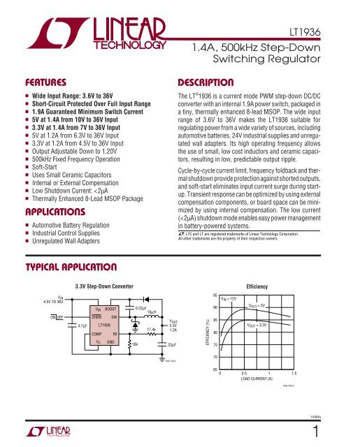
LT1936 APPLICATIO S U TYPICAL APPLICATIO U DESCRIPTIO U 1.4A ...
LT1936 APPLICATIO S U TYPICAL APPLICATIO U DESCRIPTIO U 1.4A ...
LT1936 APPLICATIO S U TYPICAL APPLICATIO U DESCRIPTIO U 1.4A ...

Create successful ePaper yourself
Turn your PDF publications into a flip-book with our unique Google optimized e-Paper software.
<strong>LT1936</strong><br />
<strong>1.4A</strong>, 500kHz Step-Down<br />
Switching Regulator<br />
FEATURES<br />
■ Wide Input Range: 3.6V to 36V<br />
■ Short-Circuit Protected Over Full Input Range<br />
■ 1.9A Guaranteed Minimum Switch Current<br />
■ 5V at <strong>1.4A</strong> from 10V to 36V Input<br />
■ 3.3V at <strong>1.4A</strong> from 7V to 36V Input<br />
■ 5V at 1.2A from 6.3V to 36V Input<br />
■ 3.3V at 1.2A from 4.5V to 36V Input<br />
■ Output Adjustable Down to 1.20V<br />
■ 500kHz Fixed Frequency Operation<br />
■ Soft-Start<br />
■ Uses Small Ceramic Capacitors<br />
■ Internal or External Compensation<br />
■ Low Shutdown Current:
<strong>LT1936</strong><br />
ABSOLUTE AXI U RATI GS<br />
W W W<br />
(Note 1)<br />
V IN Voltage ............................................... –0.4V to 36V<br />
BOOST Voltage ........................................................ 43V<br />
BOOST Above SW Voltage ....................................... 20V<br />
SHDN Voltage ........................................... –0.4V to 36V<br />
FB, V C , COMP Voltage ............................................... 6V<br />
Operating Temperature Range (Note 2)<br />
<strong>LT1936</strong>E ............................................. –40°C to 85°C<br />
<strong>LT1936</strong>I ............................................ –40°C to 125°C<br />
<strong>LT1936</strong>H .......................................... –40°C to 150°C<br />
Maximum Junction Temperature<br />
<strong>LT1936</strong>E, <strong>LT1936</strong>I ............................................ 125°C<br />
<strong>LT1936</strong>H ......................................................... 150°C<br />
Storage Temperature Range .................. –65°C to 150°C<br />
Lead Temperature (Soldering, 10 sec).................. 300°C<br />
U<br />
U U W<br />
PACKAGE/ORDER I FOR ATIO<br />
BOOST<br />
V IN<br />
SW<br />
GND<br />
1<br />
2<br />
3<br />
4<br />
TOP VIEW<br />
9<br />
8 COMP<br />
7 V C<br />
6 FB<br />
5 SHDN<br />
MS8E PACKAGE<br />
8-LEAD PLASTIC MSOP<br />
θ JA = 40°C/W, θ JC = 10°C/W<br />
EXPOSED PAD (PIN 9) IS GND<br />
MUST BE CONNECTED TO PCB<br />
ORDER PART<br />
NUMBER<br />
<strong>LT1936</strong>EMS8E<br />
<strong>LT1936</strong>IMS8E<br />
<strong>LT1936</strong>HMS8E<br />
MS8E PART MARKING<br />
LTBMT<br />
LTBRV<br />
LTBWB<br />
Order Options Tape and Reel: Add #TR<br />
Lead Free: Add #PBF Lead Free Tape and Reel: Add #TRPBF<br />
Lead Free Part Marking: http://www.linear.com/leadfree/<br />
Consult factory for parts specified with wider operating temperature ranges.<br />
ELECTRICAL CHARACTERISTICS<br />
The ● denotes specifications which apply over the full operating temperature range, otherwise specifications are at T A = 25°C.<br />
V IN = 12V, V BOOST = 17V, unless otherwise noted. (Note 2)<br />
PARAMETER CONDITIONS MIN TYP MAX UNITS<br />
Undervoltage Lockout 3.45 3.6 V<br />
Quiescent Current V FB = 1.5V 1.8 2.5 mA<br />
Quiescent Current in Shutdown V SHDN = 0V 0.1 2 µA<br />
FB Voltage ● 1.175 1.200 1.215 V<br />
FB Pin Bias Current (Note 4) V FB = 1.20V, E and I Grades ● 50 200 nA<br />
H Grade ● 50 300 nA<br />
FB Voltage Line Regulation V IN = 5V to 36V 0.01 %/V<br />
Error Amp g m V C = 0.5V, I VC = ±5µA 250 µS<br />
Error Amp Voltage Gain V C = 0.8V, 1.2V 150<br />
V C Clamp 1.8 V<br />
V C Switch Threshold 0.7 V<br />
Internal Compensation R 50 kΩ<br />
Internal Compensation C V COMP = 1V 150 pF<br />
COMP Pin Leakage V COMP = 1.8V, E and I Grades ● 1 µA<br />
H Grade ● 2 µA<br />
Switching Frequency V FB = 1.1V 400 500 600 kHz<br />
V FB = 0V 40 kHz<br />
Maximum Duty Cycle ● 87 92 %<br />
Switch Current Limit 1.9 2.2 2.6 A<br />
Switch V CESAT I SW = 1.2A 410 520 mV<br />
Switch Leakage Current 2 µA<br />
Minimum BOOST Voltage Above SW I SW = 1.2A 2 2.2 V<br />
2<br />
1936fa
ELECTRICAL CHARACTERISTICS<br />
The ● denotes specifications which apply over the full operating temperature range, otherwise specifications are at T A = 25°C.<br />
V IN = 12V, V BOOST = 17V, unless otherwise noted. (Note 2)<br />
<strong>LT1936</strong><br />
PARAMETER CONDITIONS MIN TYP MAX UNITS<br />
BOOST Pin Current I SW = 1.2A 28 50 mA<br />
BOOST Pin Leakage V SW = 0V 0.1 1 µA<br />
SHDN Input Voltage High 2.3 V<br />
SHDN Input Voltage Low 0.3 V<br />
SHDN Pin Current V SHDN = 2.3V (Note 5) 34 50 µA<br />
V SHDN = 12V 140 240 µA<br />
V SHDN = 0V 0.01 0.1 µA<br />
Note 1: Absolute Maximum Ratings are those values beyond which the life<br />
of the device may be impaired.<br />
Note 2: The <strong>LT1936</strong>E is guaranteed to meet performance specifications<br />
from 0°C to 70°C. Specifications over the –40°C to 85°C operating<br />
temperature range are assured by design, characterization and correlation<br />
with statistical process controls. The <strong>LT1936</strong>I specifications are<br />
guaranteed over the –40°C to 125°C temperature range. The <strong>LT1936</strong>H<br />
specifications are guaranteed over the –40°C to 150°C temperature range.<br />
High junction temperatures degrade operating lifetimes. Operating lifetime<br />
at junction temperatures greater than 125°C is derated to 1000 hours.<br />
Note 3: Current limit guaranteed by design and/or correlation to static test.<br />
Slope compensation reduces current limit at higher duty cycle.<br />
Note 4: Current flows out of pin.<br />
Note 5: Current flows into pin.<br />
<strong>TYPICAL</strong> PERFOR A CE CHARACTERISTICS<br />
U W<br />
Efficiency, V OUT = 5V Efficiency, V OUT = 3.3V Switch Current Limit<br />
100<br />
100<br />
3.0<br />
EFFICIENCY (%)<br />
90<br />
80<br />
70<br />
60<br />
0<br />
V IN = 12V<br />
V IN = 24V<br />
V OUT = 5V<br />
T A = 25°C<br />
D1 = DFLS140L<br />
L1 = 15µH, TOKO D63CB<br />
0.5 1.0<br />
LOAD CURRENT (A)<br />
1.5<br />
EFFICIENCY (%)<br />
90<br />
80<br />
70<br />
60<br />
0<br />
V IN = 5V<br />
V IN = 12V<br />
V IN = 24V<br />
V OUT = 3.3V<br />
T A = 25°C<br />
D1 = DFLS140L<br />
L1 = 10µH, TOKO D63CB<br />
0.5 1.0<br />
LOAD CURRENT (A)<br />
1.5<br />
CURRENT LIMIT (A)<br />
2.5<br />
2.0<br />
1.5<br />
1.0<br />
0.5<br />
0<br />
0<br />
TYP<br />
MIN<br />
20 40 60 80<br />
DUTY CYCLE (%)<br />
100<br />
1936 G01<br />
1936 G02<br />
1936 G03<br />
1936fa<br />
3
<strong>LT1936</strong><br />
<strong>TYPICAL</strong> PERFOR A CE CHARACTERISTICS<br />
U W<br />
LOAD CURRENT (A)<br />
1.8<br />
1.6<br />
1.4<br />
1.2<br />
Maximum Load Current Maximum Load Current Switch Voltage Drop<br />
V OUT = 5V<br />
L = 15µH<br />
L = 10µH<br />
LOAD CURRENT (A)<br />
1.8<br />
1.6<br />
1.4<br />
1.2<br />
V OUT = 3.3V<br />
L = 10µH<br />
L = 6.8µH<br />
SWITCH VOLTAGE DROP (mV)<br />
600<br />
500<br />
400<br />
300<br />
200<br />
100<br />
T A = 85°C<br />
T A = 25°C<br />
T A = –45°C<br />
1.0<br />
0<br />
5 10 15 20 25<br />
INPUT VOLTAGE (V)<br />
30<br />
1.0<br />
0<br />
5 10 15 20 25<br />
INPUT VOLTAGE (V)<br />
30<br />
0<br />
0<br />
0.5 1.0<br />
SWITCH CURRENT (A)<br />
1.5<br />
1936 G04<br />
1936 G05<br />
1936 G06<br />
Feedback Voltage Undervoltage Lockout Switching Frequency<br />
1.210<br />
3.8<br />
600<br />
FEEDBACK VOLTAGE (V)<br />
1.205<br />
1.200<br />
1.195<br />
1.190<br />
UVLO (V)<br />
3.6<br />
3.4<br />
3.2<br />
SWITCHING FREQUENCY (kHz)<br />
550<br />
500<br />
450<br />
1.185<br />
–50 –25 0 25 50 75 100 125 150<br />
TEMPERATURE (°C)<br />
3.0<br />
–50<br />
–25 0 25 50 75 100 125 150<br />
TEMPERATURE (°C)<br />
400<br />
–50<br />
–25 0 25 50 75 100 125 150<br />
TEMPERATURE (°C)<br />
1936 G07<br />
1936 G08<br />
1936 G09<br />
SWITCHING FREQUENCY (kHz)<br />
Frequency Foldback Soft-Start SHDN Pin Current<br />
700<br />
TA = 25°C<br />
600<br />
500<br />
400<br />
300<br />
200<br />
100<br />
SWITCH CURRENT LIMIT (A)<br />
3.0 TA = 25°C<br />
DC = 30%<br />
2.5<br />
2.0<br />
1.5<br />
1.0<br />
0.5<br />
SHDN PIN CURRENT (µA)<br />
200<br />
T A = 25°C<br />
150<br />
100<br />
50<br />
0<br />
0<br />
0.5 1.0 1.5<br />
FB PIN VOLTAGE (V)<br />
0<br />
0<br />
1 2 3 4<br />
SHDN PIN VOLTAGE (V)<br />
0<br />
0<br />
4 8 12 16<br />
SHDN PIN VOLTAGE (V)<br />
1936 G10<br />
1936 G11<br />
1936 G12<br />
4<br />
1936fa
<strong>LT1936</strong><br />
<strong>TYPICAL</strong> PERFOR A CE CHARACTERISTICS<br />
U W<br />
INPUT VOLTAGE (V)<br />
6<br />
Minimum Input Voltage<br />
8<br />
V OUT = 5V<br />
T A = 25°C<br />
L = 15µH<br />
7<br />
TO START<br />
5<br />
TO RUN<br />
INPUT VOLTAGE (V)<br />
6.0<br />
5.5<br />
5.0<br />
4.5<br />
4.0<br />
3.5<br />
Minimum Input Voltage<br />
V OUT = 3.3V<br />
T A = 25°C<br />
L = 10µH<br />
TO START<br />
TO RUN<br />
SWITCH CURRENT LIMIT (A)<br />
3.0<br />
2.5<br />
2.0<br />
1.5<br />
1.0<br />
0.5<br />
Switch Current Limit<br />
4<br />
1<br />
10 100 1000<br />
LOAD CURRENT (mA)<br />
3.0<br />
0<br />
10 100 1000<br />
LOAD CURRENT (mA)<br />
0<br />
–50<br />
–25 0 25 50 75 100 125 150<br />
TEMPERATURE (°C)<br />
1936 G13<br />
1936 G14<br />
1936 G15<br />
Switching Waveforms<br />
Switching Waveforms,<br />
Discontinuous Mode<br />
V SW<br />
10V/DIV<br />
V SW<br />
10V/DIV<br />
I L<br />
500mA/DIV<br />
I L<br />
500mA/DIV<br />
V OUT<br />
20mV/DIV<br />
V OUT<br />
20mV/DIV<br />
V IN = 12V<br />
V OUT = 3.3V<br />
I OUT = 1A<br />
L = 10µH<br />
C OUT = 22µF<br />
1µs/DIV<br />
1936 G16<br />
V IN = 12V<br />
V OUT = 3.3V<br />
I OUT = 50mA<br />
L = 10µH<br />
C OUT = 22µF<br />
1µs/DIV<br />
1936 G17<br />
2.5<br />
2.0<br />
V C Voltages<br />
60<br />
40<br />
Error Amp Output Current<br />
T A = 25°C<br />
V C = 0.5V<br />
VC VOLTAGE (V)<br />
1.5<br />
1.0<br />
CURRENT LIMIT CLAMP<br />
SWITCHING THRESHOLD<br />
V C PIN CURRENT (µA)<br />
20<br />
0<br />
–20<br />
0.5<br />
–40<br />
0<br />
–50 –25<br />
0 25 50 75 100 125 150<br />
TEMPERATURE (°C)<br />
–60<br />
0<br />
1<br />
FB PIN VOLTAGE (V)<br />
2<br />
1936 G18<br />
1936 G19<br />
1936fa<br />
5
<strong>LT1936</strong><br />
PI FU CTIO S<br />
U U U<br />
BOOST (Pin 1): The BOOST pin is used to provide a drive<br />
voltage, higher than the input voltage, to the internal<br />
bipolar NPN power switch.<br />
V IN (Pin 2): The V IN pin supplies current to the <strong>LT1936</strong>’s<br />
internal regulator and to the internal power switch. This<br />
pin must be locally bypassed.<br />
SW (Pin 3): The SW pin is the output of the internal power<br />
switch. Connect this pin to the inductor, catch diode and<br />
boost capacitor.<br />
GND (Pin 4): Tie the GND pin to a local ground plane below<br />
the <strong>LT1936</strong> and the circuit components. Return the feedback<br />
divider to this pin.<br />
SHDN (Pin 5): The SHDN pin is used to put the <strong>LT1936</strong><br />
in shutdown mode. Tie to ground to shut down the<br />
<strong>LT1936</strong>. Tie to 2.3V or more for normal operation. If the<br />
shutdown feature is not used, tie this pin to the V IN pin.<br />
SHDN also provides a soft-start function; see the Applications<br />
Information. Do not drive SHDN more than 5V<br />
above V IN .<br />
FB (Pin 6): The <strong>LT1936</strong> regulates its feedback pin to<br />
1.200V. Connect the feedback resistor divider tap to this<br />
pin. Set the output voltage according to V OUT = 1.200V<br />
(1 + R1/R2). A good value for R2 is 10k.<br />
V C (Pin 7): The V C pin is used to compensate the <strong>LT1936</strong><br />
control loop by tying an external RC network from this pin<br />
to ground. The COMP pin provides access to an internal<br />
RC network that can be used instead of the external<br />
components.<br />
COMP (Pin 8): To use the internal compensation network,<br />
tie the COMP pin to the V C pin. Otherwise, tie COMP to<br />
ground or leave it floating.<br />
Exposed Pad (Pin 9): The Exposed Pad must be soldered<br />
to the PCB and electrically connected to ground. Use a<br />
large ground plane and thermal vias to optimize thermal<br />
performance.<br />
BLOCK DIAGRA<br />
W<br />
V IN<br />
2<br />
V IN<br />
C2<br />
INT REG<br />
AND<br />
UVLO<br />
ON OFF<br />
R3<br />
SHDN<br />
5<br />
C4<br />
OSC<br />
SLOPE<br />
COMP<br />
FREQUENCY<br />
FOLDBACK<br />
Σ<br />
R<br />
S<br />
Q<br />
Q<br />
DRIVER<br />
Q1<br />
BOOST<br />
SW<br />
1<br />
3<br />
D2<br />
C3<br />
L1<br />
D1<br />
C1<br />
V OUT<br />
FB<br />
6<br />
R1<br />
R2<br />
V C<br />
g m<br />
1.200V<br />
R C<br />
50k<br />
C C<br />
150pF<br />
7 V C<br />
8<br />
COMP<br />
4<br />
GND<br />
1936 BD<br />
R4<br />
C5<br />
6<br />
1936fa
<strong>LT1936</strong><br />
OPERATIO U (Refer to Block Diagram)<br />
The <strong>LT1936</strong> is a constant frequency, current mode stepdown<br />
regulator. A 500kHz oscillator enables an RS flipflop,<br />
turning on the internal 1.9A power switch Q1. An<br />
amplifier and comparator monitor the current flowing<br />
between the V IN and SW pins, turning the switch off when<br />
this current reaches a level determined by the voltage at<br />
V C . An error amplifier measures the output voltage through<br />
an external resistor divider tied to the FB pin and servos the<br />
V C pin. If the error amplifier’s output increases, more<br />
current is delivered to the output; if it decreases, less<br />
current is delivered. An active clamp (not shown) on the V C<br />
pin provides current limit. The V C pin is also clamped to<br />
the voltage on the SHDN pin; soft-start is implemented by<br />
generating a voltage ramp at the SHDN pin using an<br />
external resistor and capacitor.<br />
An internal regulator provides power to the control circuitry.<br />
This regulator includes an undervoltage lockout to<br />
prevent switching when V IN is less than ~3.45V. The<br />
SHDN pin is used to place the <strong>LT1936</strong> in shutdown,<br />
disconnecting the output and reducing the input current to<br />
less than 2µA.<br />
The switch driver operates from either the input or from<br />
the BOOST pin. An external capacitor and diode are used<br />
to generate a voltage at the BOOST pin that is higher than<br />
the input supply. This allows the driver to fully saturate the<br />
internal bipolar NPN power switch for efficient operation.<br />
The oscillator reduces the <strong>LT1936</strong>’s operating frequency<br />
when the voltage at the FB pin is low. This frequency<br />
foldback helps to control the output current during startup<br />
and overload.<br />
1936fa<br />
7
<strong>LT1936</strong><br />
<strong>APPLICATIO</strong> S I FOR<br />
FB Resistor Network<br />
ATIO<br />
U W U U<br />
The output voltage is programmed with a resistor divider<br />
between the output and the FB pin. Choose the 1%<br />
resistors according to:<br />
⎛<br />
R R V OUT ⎞<br />
1=<br />
2⎜<br />
– 1⎟<br />
⎝ 1 . 200 ⎠<br />
R2 should be 20k or less to avoid bias current errors.<br />
Reference designators refer to the Block Diagram.<br />
Input Voltage Range<br />
The input voltage range for <strong>LT1936</strong> applications depends<br />
on the output voltage and the Absolute Maximum Ratings<br />
of the V IN and BOOST pins.<br />
The minimum input voltage is determined by either the<br />
<strong>LT1936</strong>’s minimum operating voltage of ~3.45V or by its<br />
maximum duty cycle. The duty cycle is the fraction of time<br />
that the internal switch is on and is determined by the input<br />
and output voltages:<br />
VOUT<br />
+ VD<br />
DC =<br />
V – V + V<br />
IN SW D<br />
where V D is the forward voltage drop of the catch diode<br />
(~0.5V) and V SW is the voltage drop of the internal switch<br />
(~0.5V at maximum load). This leads to a minimum input<br />
voltage of:<br />
V<br />
VOUT<br />
+ V<br />
=<br />
DC<br />
D<br />
IN( MIN) –<br />
MAX<br />
with DC MAX = 0.87.<br />
V<br />
D<br />
+ V<br />
SW<br />
The maximum input voltage is determined by the absolute<br />
maximum ratings of the V IN and BOOST pins and by the<br />
minimum duty cycle DC MIN = 0.08:<br />
V<br />
VOUT<br />
+ V<br />
=<br />
DC<br />
D<br />
IN( MAX) –<br />
MIN<br />
V<br />
D<br />
+ V<br />
SW<br />
Note that this is a restriction on the operating input<br />
voltage; the circuit will tolerate transient inputs up to the<br />
absolute maximum ratings of the V IN and BOOST pins.<br />
Inductor Selection and Maximum Output Current<br />
A good first choice for the inductor value is<br />
L = 2.2 (V OUT + V D )<br />
where V D is the voltage drop of the catch diode (~0.4V) and<br />
L is in µH. With this value the maximum output current will<br />
be above 1.2A at all duty cycles and greater than <strong>1.4A</strong> for<br />
duty cycles less than 50% (V IN > 2 V OUT ). The inductor’s<br />
RMS current rating must be greater than the maximum<br />
load current and its saturation current should be about<br />
30% higher. For robust operation in fault conditions<br />
(start-up or short circuit) and high input voltage (>30V),<br />
the saturation current should be above 2.6A. To keep the<br />
efficiency high, the series resistance (DCR) should be less<br />
than 0.1Ω, and the core material should be intended for<br />
high frequency applications. Table 1 lists several vendors<br />
and suitable types.<br />
Table 1. Inductor Vendors<br />
VENDOR URL PART SERIES TYPE<br />
Murata www.murata.com LQH55D Open<br />
TDK www.component.tdk.com SLF7045 Shielded<br />
SLF10145 Shielded<br />
Toko www.toko.com D62CB Shielded<br />
D63CB<br />
Shielded<br />
D75C<br />
Shielded<br />
D75F<br />
Open<br />
Sumida www.sumida.com CR54 Open<br />
CDRH74<br />
Shielded<br />
CDRH6D38 Shielded<br />
CR75<br />
Open<br />
Of course, such a simple design guide will not always result<br />
in the optimum inductor for your application. A larger<br />
value provides a slightly higher maximum load current and<br />
will reduce the output voltage ripple. If your load is lower<br />
than 1.2A, then you can decrease the value of the inductor<br />
and operate with higher ripple current. This allows you to<br />
use a physically smaller inductor, or one with a lower DCR<br />
resulting in higher efficiency. Be aware that if the inductance<br />
differs from the simple rule above, then the maximum load<br />
current will depend on input voltage. There are several<br />
graphs in the Typical Performance Characteristics section<br />
8<br />
1936fa
<strong>LT1936</strong><br />
<strong>APPLICATIO</strong> S I FOR<br />
ATIO<br />
U W U U<br />
of this data sheet that show the maximum load current as<br />
a function of input voltage and inductor value for several<br />
popular output voltages. Low inductance may result in<br />
discontinuous mode operation, which is okay but further<br />
reduces maximum load current. For details of maximum<br />
output current and discontinuous mode operation, see<br />
Linear Technology Application Note 44. Finally, for duty<br />
cycles greater than 50% (V OUT /V IN > 0.5), there is a minimum<br />
inductance required to avoid subharmonic oscillations.<br />
Choosing L greater than 1.6 (V OUT + V D ) µH prevents<br />
subharmonic oscillations at all duty cycles.<br />
Catch Diode<br />
A 1A Schottky diode is recommended for the catch diode,<br />
D1. The diode must have a reverse voltage rating equal to<br />
or greater than the maximum input voltage. The ON<br />
Semiconductor MBRM140 is a good choice. It is rated for<br />
1A DC at a case temperature of 110°C and 1.5A at a case<br />
temperature of 95°C. Diode Incorporated’s DFLS140L is<br />
rated for 1.1A average current; the DFLS240L is rated for<br />
2A average current. The average diode current in an<br />
<strong>LT1936</strong> application is approximately I OUT (1 – DC).<br />
Input Capacitor<br />
Bypass the input of the <strong>LT1936</strong> circuit with a 4.7µF or<br />
higher value ceramic capacitor of X7R or X5R type. Y5V<br />
types have poor performance over temperature and applied<br />
voltage, and should not be used. A 4.7µF ceramic is<br />
adequate to bypass the <strong>LT1936</strong> and will easily handle the<br />
ripple current. However, if the input power source has high<br />
impedance, or there is significant inductance due to long<br />
wires or cables, additional bulk capacitance may be necessary.<br />
This can be provided with a low performance<br />
electrolytic capacitor.<br />
Step-down regulators draw current from the input supply<br />
in pulses with very fast rise and fall times. The input<br />
capacitor is required to reduce the resulting voltage ripple<br />
at the <strong>LT1936</strong> and to force this very high frequency<br />
switching current into a tight local loop, minimizing EMI.<br />
A 4.7µF capacitor is capable of this task, but only if it is<br />
placed close to the <strong>LT1936</strong> and the catch diode; see the<br />
PCB Layout section. A second precaution regarding the<br />
ceramic input capacitor concerns the maximum input<br />
voltage rating of the <strong>LT1936</strong>. A ceramic input capacitor<br />
combined with trace or cable inductance forms a high<br />
quality (under damped) tank circuit. If the <strong>LT1936</strong> circuit<br />
is plugged into a live supply, the input voltage can ring to<br />
twice its nominal value, possibly exceeding the <strong>LT1936</strong>’s<br />
voltage rating. This situation is easily avoided; see the Hot<br />
Plugging Safety section.<br />
For space sensitive applications, a 2.2µF ceramic capacitor<br />
can be used for local bypassing of the <strong>LT1936</strong> input.<br />
However, the lower input capacitance will result in increased<br />
input current ripple and input voltage ripple, and<br />
may couple noise into other circuitry. Also, the increased<br />
voltage ripple will raise the minimum operating voltage of<br />
the <strong>LT1936</strong> to ~3.7V.<br />
Output Capacitor<br />
The output capacitor has two essential functions. Along<br />
with the inductor, it filters the square wave generated by<br />
the <strong>LT1936</strong> to produce the DC output. In this role it<br />
determines the output ripple, and low impedance at the<br />
switching frequency is important. The second function is<br />
to store energy in order to satisfy transient loads and<br />
stabilize the <strong>LT1936</strong>’s control loop.<br />
Ceramic capacitors have very low equivalent series resistance<br />
(ESR) and provide the best ripple performance. A<br />
good value is:<br />
COUT<br />
= 150<br />
VOUT<br />
where C OUT is in µF. Use X5R or X7R types. This choice will<br />
provide low output ripple and good transient response.<br />
Transient performance can be improved with a high value<br />
capacitor if the compensation network is also adjusted to<br />
maintain the loop bandwidth.<br />
A lower value of output capacitor can be used, but transient<br />
performance will suffer. With an external compensation<br />
network, the loop gain can be lowered to compensate<br />
for the lower capacitor value. When using the internal<br />
compensation network, the lowest value for stable operation<br />
is:<br />
COUT<br />
> 66<br />
V<br />
OUT<br />
1936fa<br />
9
<strong>LT1936</strong><br />
<strong>APPLICATIO</strong> S I FOR<br />
ATIO<br />
U W U U<br />
Table 2. Capacitor Vendors<br />
Vendor Phone URL Part Series Comments<br />
Panasonic (714) 373-7366 www.panasonic.com Ceramic,<br />
Polymer, EEF Series<br />
Tantalum<br />
Kemet (864) 963-6300 www.kemet.com Ceramic,<br />
Tantalum<br />
Sanyo (408) 749-9714 www.sanyovideo.com Ceramic,<br />
Polymer,<br />
Tantalum<br />
Murata (404) 436-1300 www.murata.com Ceramic<br />
AVX www.avxcorp.com Ceramic,<br />
Tantalum<br />
Taiyo Yuden (864) 963-6300 www.taiyo-yuden.com Ceramic<br />
T494, T495<br />
POSCAP<br />
TPS Series<br />
This is the minimum output capacitance required, not the<br />
nominal capacitor value. For example, a 3.3V output<br />
requires 20µF of output capacitance. If a small 22µF, 6.3V<br />
ceramic capacitor is used, the circuit may be unstable<br />
because the effective capacitance is lower than the nominal<br />
capacitance when biased at 3.3V. Look carefully at the<br />
capacitor’s data sheet to find out what the actual capacitance<br />
is under operating conditions (applied voltage and<br />
temperature). A physically larger capacitor, or one with a<br />
higher voltage rating, may be required.<br />
High performance electrolytic capacitors can be used for<br />
the output capacitor. Low ESR is important, so choose one<br />
that is intended for use in switching regulators. The ESR<br />
should be specified by the supplier, and should be 0.05Ω<br />
or less. Such a capacitor will be larger than a ceramic<br />
capacitor and will have a larger capacitance, because the<br />
capacitor must be large to achieve low ESR. Table 2 lists<br />
several capacitor vendors.<br />
Frequency Compensation<br />
The <strong>LT1936</strong> uses current mode control to regulate the<br />
output. This simplifies loop compensation. In particular,<br />
the <strong>LT1936</strong> does not require the ESR of the output capacitor<br />
for stability, so you are free to use ceramic capacitors<br />
to achieve low output ripple and small circuit size.<br />
Frequency compensation is provided by the components<br />
tied to the V C pin, as shown in Figure 1. Generally a<br />
capacitor (C C ) and a resistor (R C ) in series to ground are<br />
used. In addition, there may be lower value capacitor in<br />
10<br />
parallel. This capacitor (C F ) is not part of the loop compensation<br />
but is used to filter noise at the switching frequency,<br />
and is required only if a phase-lead capacitor is used or if<br />
the output capacitor has high ESR. An alternative to using<br />
external compensation components is to use the internal<br />
RC network by tying the COMP pin to the V C pin. This<br />
reduces component count but does not provide the optimum<br />
transient response when the output capacitor value<br />
is high, and the circuit may not be stable when the output<br />
capacitor value is low. If the internal compensation network<br />
is not used, tie COMP to ground or leave it floating.<br />
Loop compensation determines the stability and transient<br />
performance. Designing the compensation network is a<br />
<strong>LT1936</strong><br />
CURRENT MODE<br />
POWER STAGE<br />
g m = 2mho<br />
C F<br />
600k<br />
–<br />
+<br />
150pF<br />
50k<br />
V C COMP GND<br />
R C<br />
C C<br />
ERROR<br />
AMPLIFIER<br />
g m =<br />
250µmho<br />
SW<br />
FB<br />
1.25V<br />
R1<br />
R2<br />
C PL<br />
ESR<br />
C1<br />
+<br />
POLYMER<br />
OR<br />
TANTALUM<br />
Figure 1. Model for Loop Response<br />
OUTPUT<br />
1936 F01<br />
C1<br />
CERAMIC<br />
1936fa
<strong>LT1936</strong><br />
<strong>APPLICATIO</strong> S I FOR<br />
ATIO<br />
U W U U<br />
bit complicated and the best values depend on the application<br />
and in particular the type of output capacitor. A<br />
practical approach is to start with one of the circuits in this<br />
data sheet that is similar to your application and tune the<br />
compensation network to optimize the performance. Stability<br />
should then be checked across all operating conditions,<br />
including load current, input voltage and temperature.<br />
The LT1375 data sheet contains a more thorough discussion<br />
of loop compensation and describes how to test the<br />
stability using a transient load.<br />
Figure 1 shows an equivalent circuit for the <strong>LT1936</strong> control<br />
loop. The error amplifier is a transconductance amplifier<br />
with finite output impedance. The power section, consisting<br />
of the modulator, power switch and inductor, is<br />
modeled as a transconductance amplifier generating an<br />
output current proportional to the voltage at the V C pin.<br />
Note that the output capacitor integrates this current, and<br />
that the capacitor on the V C pin (C C ) integrates the error<br />
amplifier output current, resulting in two poles in the loop.<br />
In most cases a zero is required and comes from either the<br />
output capacitor ESR or from a resistor R C in series with<br />
C C . This simple model works well as long as the value of<br />
the inductor is not too high and the loop crossover<br />
frequency is much lower than the switching frequency. A<br />
phase lead capacitor (C PL ) across the feedback divider<br />
may improve the transient response.<br />
Figure 2 compares the transient response across several<br />
output capacitor choices and compensation schemes. In<br />
each case the load current is stepped from 200mA to<br />
800mA and back to 200mA.<br />
C OUT = 22µF<br />
(AVX 1210ZD226MAT)<br />
(2a)<br />
COMP<br />
V C<br />
V OUT<br />
100mV/DIV<br />
C OUT = 22µF ×2<br />
(2b)<br />
COMP<br />
V C<br />
V OUT<br />
100mV/DIV<br />
(2c)<br />
C OUT = 150µF<br />
(4TPC150M)<br />
COMP<br />
V C<br />
V OUT<br />
100mV/DIV<br />
C OUT = 150µF<br />
(4TPC150M)<br />
V OUT<br />
100mV/DIV<br />
(2d)<br />
COMP<br />
V C<br />
220k<br />
100pF<br />
800mA<br />
I OUT<br />
500mA/DIV<br />
200mA<br />
50µs/DIV<br />
1936 F02<br />
Figure 2. Transient Load Response of the <strong>LT1936</strong> with Different Output<br />
Capacitors as the Load Current is Stepped from 200mA to 800mA. V OUT = 3.3V<br />
1936fa<br />
11
<strong>LT1936</strong><br />
<strong>APPLICATIO</strong> S I FOR<br />
BOOST Pin Considerations<br />
12<br />
ATIO<br />
U W U U<br />
Capacitor C3 and diode D2 are used to generate a boost<br />
voltage that is higher than the input voltage. In most cases<br />
a 0.22µF capacitor and fast switching diode (such as the<br />
1N4148 or 1N914) will work well. Figure 3 shows two<br />
ways to arrange the boost circuit. The BOOST pin must be<br />
at least 2.3V above the SW pin for best efficiency. For<br />
outputs of 3V and above, the standard circuit (Figure 3a)<br />
is best. For outputs between 2.8V and 3V, use a 0.47µF<br />
capacitor and a Schottky diode. For lower output voltages<br />
the boost diode can be tied to the input (Figure 3b), or to<br />
another supply greater than 2.8V. The circuit in Figure 3a<br />
is more efficient because the BOOST pin current comes<br />
from a lower voltage. You must also be sure that the<br />
maximum voltage rating of the BOOST pin is not exceeded.<br />
A 2.5V output presents a special case. This is a popular<br />
output voltage, and the advantage of connecting the boost<br />
circuit to the output is that the circuit will accept a 36V<br />
maximum input voltage rather than 20V (due to the<br />
BOOST pin rating). However, 2.5V is marginally adequate<br />
to support the boosted drive stage at low ambient temperatures.<br />
Therefore, special care and some restrictions<br />
on operation are necessary when powering the BOOST pin<br />
from a 2.5V output. Minimize the voltage loss in the boost<br />
circuit by using a 1µF boost capacitor and a good, low drop<br />
V IN<br />
V IN<br />
BOOST<br />
<strong>LT1936</strong><br />
V IN SW<br />
GND<br />
V BOOST – V SW ≅ V OUT<br />
MAX V BOOST ≅ V IN + V OUT<br />
(3a)<br />
D2<br />
BOOST<br />
<strong>LT1936</strong><br />
V IN SW<br />
GND<br />
V BOOST – V SW ≅ V IN<br />
MAX V BOOST ≅ 2V IN<br />
(3b)<br />
Figure 3. Two Circuits for Generating the Boost Voltage<br />
C3<br />
C3<br />
D2<br />
1933 F03<br />
V OUT<br />
V OUT<br />
Schottky diode (such as the ON Semi MBR0540). Because<br />
the required boost voltage increases at low temperatures,<br />
the circuit will supply only 1A of output current when the<br />
ambient temperature is –45°C, increasing to 1.2A at 0°C.<br />
Also, the minimum input voltage to start the boost circuit<br />
is higher at low temperature. See the Typical Applications<br />
section for a 2.5V schematic and performance curves.<br />
The minimum operating voltage of an <strong>LT1936</strong> application<br />
is limited by the undervoltage lockout (~3.45V) and by the<br />
maximum duty cycle as outlined above. For proper startup,<br />
the minimum input voltage is also limited by the boost<br />
circuit. If the input voltage is ramped slowly, or the <strong>LT1936</strong><br />
is turned on with its SHDN pin when the output is already<br />
in regulation, then the boost capacitor may not be fully<br />
charged. Because the boost capacitor is charged with the<br />
energy stored in the inductor, the circuit will rely on some<br />
minimum load current to get the boost circuit running<br />
properly. This minimum load will depend on input and<br />
output voltages, and on the arrangement of the boost<br />
circuit. The minimum load generally goes to zero once the<br />
circuit has started. Figure 4 shows a plot of minimum load<br />
to start and to run as a function of input voltage. In many<br />
cases the discharged output capacitor will present a load<br />
to the switcher, which will allow it to start. The plots show<br />
the worst-case situation where V IN is ramping very slowly.<br />
For lower start-up voltage, the boost diode can be tied to<br />
V IN ; however, this restricts the input range to one-half of<br />
the absolute maximum rating of the BOOST pin.<br />
At light loads, the inductor current becomes discontinuous<br />
and the effective duty cycle can be very high. This<br />
reduces the minimum input voltage to approximately<br />
300mV above V OUT . At higher load currents, the inductor<br />
current is continuous and the duty cycle is limited by the<br />
maximum duty cycle of the <strong>LT1936</strong>, requiring a higher<br />
input voltage to maintain regulation.<br />
Soft-Start<br />
The SHDN pin can be used to soft-start the <strong>LT1936</strong>,<br />
reducing the maximum input current during start-up. The<br />
SHDN pin is driven through an external RC filter to create<br />
a voltage ramp at this pin. Figure 5 shows the start-up<br />
waveforms with and without the soft-start circuit. By<br />
choosing a large RC time constant, the peak start-up<br />
1936fa
<strong>LT1936</strong><br />
<strong>APPLICATIO</strong> S I FOR<br />
INPUT VOLTAGE (V)<br />
6.0<br />
5.5<br />
5.0<br />
4.5<br />
4.0<br />
3.5<br />
ATIO<br />
U W U U<br />
Minimum Input Voltage V OUT = 3.3V<br />
V OUT = 3.3V<br />
T A = 25°C<br />
L = 10µH<br />
TO START<br />
TO RUN<br />
INPUT VOLTAGE (V)<br />
8<br />
7<br />
6<br />
5<br />
Minimum Input Voltage V OUT = 5V<br />
V OUT = 5V<br />
T A = 25°C<br />
L = 15µH<br />
TO START<br />
TO RUN<br />
3.0<br />
0<br />
10 100 1000<br />
LOAD CURRENT (mA)<br />
4<br />
1<br />
10 100 1000<br />
LOAD CURRENT (mA)<br />
1936 G14<br />
1936 G13<br />
Figure 4. The Minimum Input Voltage Depends on Output Voltage, Load Current and Boost Circuit<br />
RUN<br />
5V/DIV<br />
RUN<br />
SHDN<br />
GND<br />
I IN<br />
500mA/DIV<br />
V OUT<br />
5V/DIV<br />
50µs/DIV<br />
1936 F05a<br />
RUN<br />
15k<br />
0.22µF<br />
SHDN<br />
GND<br />
RUN<br />
5V/DIV<br />
I IN<br />
500mA/DIV<br />
V OUT<br />
5V/DIV<br />
0.5ms/DIV<br />
1936 F05b<br />
Figure 5. To Soft-Start the <strong>LT1936</strong>, Add a Resistor and Capacitor to the SHDN Pin.<br />
V IN = 12V, V OUT = 3.3V, C OUT = 2 × 22µF, R LOAD = 3.3Ω<br />
current can be reduced to the current that is required to<br />
regulate the output, with no overshoot. Choose the value<br />
of the resistor so that it can supply 60µA when the SHDN<br />
pin reaches 2.3V.<br />
Shorted and Reversed Input Protection<br />
If the inductor is chosen so that it won’t saturate excessively,<br />
an <strong>LT1936</strong> buck regulator will tolerate a shorted<br />
output. There is another situation to consider in systems<br />
where the output will be held high when the input to the<br />
<strong>LT1936</strong> is absent. This may occur in battery charging<br />
applications or in battery backup systems where a battery<br />
or some other supply is diode OR-ed with the <strong>LT1936</strong>’s<br />
output. If the V IN pin is allowed to float and the SHDN pin<br />
is held high (either by a logic signal or because it is tied to<br />
V IN ), then the <strong>LT1936</strong>’s internal circuitry will pull its<br />
quiescent current through its SW pin. This is fine if your<br />
system can tolerate a few mA in this state. If you ground<br />
1936fa<br />
13
<strong>LT1936</strong><br />
<strong>APPLICATIO</strong> S I FOR<br />
ATIO<br />
U W U U<br />
the SHDN pin, the SW pin current will drop to essentially<br />
zero. However, if the V IN pin is grounded while the output<br />
is held high, then parasitic diodes inside the <strong>LT1936</strong> can<br />
pull large currents from the output through the SW pin and<br />
the V IN pin. Figure 6 shows a circuit that will run only when<br />
the input voltage is present and that protects against a<br />
shorted or reversed input.<br />
V IN<br />
D4<br />
MBRS140<br />
V IN BOOST<br />
<strong>LT1936</strong><br />
SHDN SW<br />
V C<br />
COMP GND FB<br />
V OUT<br />
BACKUP<br />
MINIMIZE<br />
<strong>LT1936</strong><br />
C2, D1 LOOP<br />
D2<br />
VIAS<br />
C3<br />
OUT<br />
L1<br />
IN<br />
C2<br />
D1<br />
C1<br />
GND<br />
GND<br />
Figure 7. A Good PCB Layout Ensures Low EMI Operation<br />
R2<br />
R1<br />
1936 F07<br />
R4<br />
1936 F06<br />
Figure 6. Diode D4 Prevents a Shorted Input from Discharging<br />
a Backup Battery Tied to the Output; It Also Protects the Circuit<br />
from a Reversed Input. The <strong>LT1936</strong> Runs Only When the Input<br />
is Present<br />
PCB Layout<br />
For proper operation and minimum EMI, care must be<br />
taken during printed circuit board layout. Figure 7 shows<br />
the recommended component placement with trace, ground<br />
plane and via locations. Note that large, switched currents<br />
flow in the <strong>LT1936</strong>’s V IN and SW pins, the catch diode (D1)<br />
and the input capacitor (C2). The loop formed by these<br />
components should be as small as possible. These components,<br />
along with the inductor and output capacitor,<br />
should be placed on the same side of the circuit board, and<br />
their connections should be made on that layer. Place a<br />
local, unbroken ground plane below these components.<br />
The SW and BOOST nodes should be as small as possible.<br />
Finally, keep the FB and V C nodes small so that the ground<br />
traces will shield them from the SW and BOOST nodes.<br />
The Exposed Pad on the bottom of the package must be<br />
soldered to ground so that the pad acts as a heat sink. To<br />
keep thermal resistance low, extend the ground plane as<br />
much as possible, and add thermal vias under and near the<br />
<strong>LT1936</strong> to additional ground planes within the circuit<br />
board and on the bottom side.<br />
High Temperature Considerations<br />
The die temperature of the <strong>LT1936</strong> must be lower than the<br />
maximum rating of 125°C (150°C for the H grade). This is<br />
generally not a concern unless the ambient temperature is<br />
above 85°C. For higher temperatures, care should be<br />
taken in the layout of the circuit to ensure good heat<br />
sinking of the <strong>LT1936</strong>. The maximum load current should<br />
be derated as the ambient temperature approaches 125°C<br />
(150°C for the H grade).<br />
The die temperature is calculated by multiplying the <strong>LT1936</strong><br />
power dissipation by the thermal resistance from junction<br />
to ambient. Power dissipation within the <strong>LT1936</strong> can be<br />
estimated by calculating the total power loss from an<br />
efficiency measurement and subtracting the catch diode<br />
loss. The resulting temperature rise at full load is nearly<br />
independent of input voltage. Thermal resistance depends<br />
on the layout of the circuit board, but values from 40°C/W<br />
to 60°C/W are typical.<br />
Die temperature rise was measured on a 4-layer, 5cm ×<br />
6.5cm circuit board in still air at a load current of <strong>1.4A</strong>. For<br />
12V input to 3.3V output the die temperature elevation<br />
above ambient was 26°C; for 24V in to 3.3V out the rise<br />
was 31°C; for 12V in to 5V the rise was 31°C and for 24V<br />
in to 5V the rise was 34°C.<br />
14<br />
1936fa
<strong>LT1936</strong><br />
<strong>APPLICATIO</strong> S I FOR<br />
Hot Plugging Safely<br />
ATIO<br />
U W U U<br />
The small size, robustness and low impedance of ceramic<br />
capacitors make them an attractive option for the input<br />
bypass capacitor of <strong>LT1936</strong> circuits. However, these capacitors<br />
can cause problems if the <strong>LT1936</strong> is plugged into<br />
a live supply (see Linear Technology Application Note 88<br />
for a complete discussion). The low loss ceramic capacitor<br />
combined with stray inductance in series with the<br />
power source forms an under damped tank circuit, and the<br />
voltage at the V IN pin of the <strong>LT1936</strong> can ring to twice the<br />
nominal input voltage, possibly exceeding the <strong>LT1936</strong>’s<br />
rating and damaging the part. If the input supply is poorly<br />
controlled or the user will be plugging the <strong>LT1936</strong> into an<br />
energized supply, the input network should be designed to<br />
prevent this overshoot.<br />
Figure 8 shows the waveforms that result when an <strong>LT1936</strong><br />
circuit is connected to a 24V supply through six feet of<br />
24-gauge twisted pair. The first plot is the response with<br />
a 4.7µF ceramic capacitor at the input. The input voltage<br />
rings as high as 50V and the input current peaks at 26A. One<br />
+<br />
CLOSING SWITCH<br />
SIMULATES HOT PLUG<br />
I IN V IN<br />
4.7µF<br />
<strong>LT1936</strong><br />
V IN<br />
20V/DIV<br />
DANGER<br />
RINGING V IN MAY EXCEED<br />
ABSOLUTE MAXIMUM<br />
RATING OF THE <strong>LT1936</strong><br />
LOW<br />
IMPEDANCE<br />
ENERGIZED<br />
24V SUPPLY<br />
STRAY<br />
INDUCTANCE<br />
DUE TO 6 FEET<br />
(2 METERS) OF<br />
TWISTED PAIR<br />
(8a)<br />
I IN<br />
10A/DIV<br />
20µs/DIV<br />
+<br />
22µF<br />
35V<br />
AI.EI.<br />
+<br />
4.7µF<br />
<strong>LT1936</strong><br />
V IN<br />
20V/DIV<br />
I IN<br />
10A/DIV<br />
(8b)<br />
20µs/DIV<br />
+<br />
0.1µF<br />
0.7Ω<br />
4.7µF<br />
<strong>LT1936</strong><br />
V IN<br />
20V/DIV<br />
I IN<br />
10A/DIV<br />
(8c)<br />
20µs/DIV<br />
1936 F08<br />
Figure 8. A Well Chosen Input Network Prevents Input Voltage Overshoot and<br />
Ensures Reliable Operation When the <strong>LT1936</strong> is Connected to a Live Supply<br />
1936fa<br />
15
<strong>LT1936</strong><br />
<strong>APPLICATIO</strong> S I FOR<br />
ATIO<br />
U W U U<br />
method of damping the tank circuit is to add another capacitor<br />
with a series resistor to the circuit. In Figure 8b an<br />
aluminum electrolytic capacitor has been added. This<br />
capacitor’s high equivalent series resistance damps the<br />
circuit and eliminates the voltage overshoot. The extra<br />
capacitor improves low frequency ripple filtering and can<br />
slightly improve the efficiency of the circuit, though it is likely<br />
to be the largest component in the circuit. An alternative<br />
solution is shown in Figure 8c. A 0.7Ω resistor is added in<br />
series with the input to eliminate the voltage overshoot (it<br />
also reduces the peak input current). A 0.1µF capacitor<br />
improves high frequency filtering. This solution is smaller<br />
and less expensive than the electrolytic capacitor. For high<br />
input voltages its impact on efficiency is minor, reducing<br />
efficiency by one percent for a 5V output at full load operating<br />
from 24V.<br />
Other Linear Technology Publications<br />
Application Notes 19, 35 and 44 contain more detailed<br />
descriptions and design information for buck regulators<br />
and other switching regulators. The LT1376 data sheet<br />
has a more extensive discussion of output ripple, loop<br />
compensation and stability testing. Design Note 100 shows<br />
how to generate a bipolar output supply using a buck<br />
regulator.<br />
<strong>TYPICAL</strong> <strong>APPLICATIO</strong> S<br />
U<br />
3.3V Step-Down Converter<br />
V IN<br />
4.5V TO 36V<br />
ON OFF<br />
C1<br />
4.7µF<br />
V IN BOOST<br />
SHDN SW<br />
<strong>LT1936</strong><br />
COMP FB<br />
C3<br />
0.22µF<br />
D1<br />
D2<br />
L1<br />
10µH<br />
R1<br />
17.4k<br />
V OUT<br />
3.3V<br />
1.2A<br />
V C<br />
GND<br />
R2<br />
10k<br />
C2<br />
47µF<br />
1936 TA03<br />
5V Step-Down Converter<br />
V IN<br />
6.3V TO 36V<br />
ON OFF<br />
C1<br />
4.7µF<br />
V IN BOOST<br />
SHDN SW<br />
<strong>LT1936</strong><br />
COMP FB<br />
C3<br />
0.22µF<br />
D1<br />
D2<br />
L1<br />
15µH<br />
R1<br />
31.6k<br />
V OUT<br />
5V<br />
1.2A<br />
V C<br />
GND<br />
R2<br />
10k<br />
C2<br />
22µF<br />
1936 TA04<br />
16<br />
1936fa
<strong>TYPICAL</strong> <strong>APPLICATIO</strong> S<br />
U<br />
1.8V Step-Down Converter<br />
Efficiency, 1.8V Output<br />
<strong>LT1936</strong><br />
V IN<br />
3.6V TO 20V<br />
ON OFF<br />
C1<br />
4.7µF<br />
V IN<br />
SHDN<br />
COMP<br />
V C<br />
D1: DFLS140L<br />
D2: 1N4148<br />
L1: TOKO D63CB<br />
D2<br />
<strong>LT1936</strong><br />
BOOST<br />
SW<br />
GND<br />
FB<br />
C3<br />
0.22µF<br />
R2<br />
20k<br />
D1<br />
L1<br />
4.7µH<br />
R1<br />
10k<br />
V OUT<br />
1.8V<br />
1.3A<br />
C2<br />
47µF<br />
×2<br />
1936 TA05a<br />
EFFICIENCY (%)<br />
90<br />
80<br />
70<br />
60<br />
50<br />
0<br />
V OUT = 1.8V<br />
T A = 25°C<br />
V IN = 12V<br />
V IN = 5V<br />
0.5 1<br />
LOAD CURRENT (A)<br />
POWER LOSS<br />
2.0<br />
1.5<br />
1.0<br />
0.5<br />
0<br />
1.5<br />
POWER LOSS (W)<br />
1936 TA05b<br />
1.2V Step-Down Converter<br />
Efficiency, 1.2V Output<br />
V IN<br />
3.6V TO 20V<br />
ON OFF<br />
C1<br />
4.7µF<br />
V IN<br />
SHDN<br />
COMP<br />
V C<br />
D1: DFLS140L<br />
D2: 1N4148<br />
L1: TOKO D63CB<br />
D2<br />
<strong>LT1936</strong><br />
BOOST<br />
SW<br />
GND<br />
FB<br />
C3<br />
0.22µF<br />
100k<br />
D1<br />
L1<br />
3.3µH<br />
V OUT<br />
1.2V<br />
1.3A<br />
C2<br />
47µF<br />
×2<br />
1936 TA06a<br />
EFFICIENCY (%)<br />
80<br />
75<br />
70<br />
65<br />
60<br />
55<br />
50<br />
0<br />
V OUT = 1.2V<br />
T A = 25°C<br />
V IN = 5V<br />
V IN = 12V<br />
0.5 1<br />
LOAD CURRENT (A)<br />
POWER LOSS<br />
2.0<br />
1.5<br />
1.0<br />
0.5<br />
0<br />
1.5<br />
POWER LOSS (W)<br />
1936 TA06b<br />
1936fa<br />
17
<strong>LT1936</strong><br />
<strong>TYPICAL</strong> <strong>APPLICATIO</strong> S<br />
U<br />
2.5V Step-Down Converter<br />
D2<br />
V IN<br />
3.6V TO 36V<br />
ON OFF<br />
C1<br />
4.7µF<br />
V IN BOOST<br />
SHDN SW<br />
<strong>LT1936</strong><br />
COMP FB<br />
C3<br />
1µF<br />
D1<br />
L1<br />
6.2µH<br />
R1<br />
11k<br />
V OUT<br />
2.5V<br />
1.2A<br />
T A > 0°C<br />
V C<br />
GND<br />
R2<br />
10k<br />
C2<br />
47µF<br />
D1: DFLS140L<br />
D2: MBRO540<br />
L1: TOKO D63CB<br />
1936 TA07a<br />
Efficiency, 2.5V Output<br />
Minimum Input Voltage<br />
EFFICIENCY (%)<br />
100<br />
90<br />
80<br />
70<br />
60<br />
0<br />
V OUT = 2.5V<br />
T A = 25°C<br />
V IN = 12V<br />
V IN = 5V<br />
0.5 1.0<br />
LOAD CURRENT (A)<br />
1.5<br />
INPUT VOLTAGE (V)<br />
5.5 VOUT = 2.5V<br />
5.0<br />
4.5<br />
4.0<br />
3.5<br />
3.0<br />
1<br />
TO RUN<br />
T A = –45°C<br />
TO RUN<br />
T A = 25°C<br />
TO START<br />
T A = –45°C<br />
TO START<br />
T A = 25°C<br />
10 100 1000<br />
LOAD CURRENT (mA)<br />
1936 TA07b<br />
1936 TA07c<br />
18<br />
1936fa
<strong>LT1936</strong><br />
PACKAGE <strong>DESCRIPTIO</strong>N<br />
U<br />
MS8E Package<br />
8-Lead Plastic MSOP<br />
(Reference LTC DWG # 05-08-1662)<br />
2.794 ± 0.102<br />
(.110 ± .004)<br />
0.889 ± 0.127<br />
(.035 ± .005)<br />
BOTTOM VIEW OF<br />
EXPOSED PAD OPTION<br />
1<br />
2.06 ± 0.102<br />
(.081 ± .004)<br />
1.83 ± 0.102<br />
(.072 ± .004)<br />
5.23<br />
(.206)<br />
MIN<br />
2.083 ± 0.102 3.20 – 3.45<br />
(.082 ± .004) (.126 – .136)<br />
0.42 ± 0.038<br />
(.0165 ± .0015)<br />
TYP<br />
0.65<br />
(.0256)<br />
BSC<br />
3.00 ± 0.102<br />
(.118 ± .004)<br />
(NOTE 3)<br />
8<br />
8<br />
7 6 5<br />
0.52<br />
(.0205)<br />
REF<br />
RECOMMENDED SOLDER PAD LAYOUT<br />
GAUGE PLANE<br />
0.18<br />
(.007)<br />
0.254<br />
(.010)<br />
DETAIL “A”<br />
NOTE:<br />
1. DIMENSIONS IN MILLIMETER/(INCH)<br />
2. DRAWING NOT TO SCALE<br />
0° – 6° TYP<br />
0.53 ± 0.152<br />
(.021 ± .006)<br />
DETAIL “A”<br />
SEATING<br />
PLANE<br />
4.90 ± 0.152<br />
(.193 ± .006)<br />
1.10<br />
(.043)<br />
MAX<br />
0.22 – 0.38<br />
(.009 – .015)<br />
TYP<br />
0.65<br />
(.0256)<br />
BSC<br />
1 2 3 4<br />
3. DIMENSION DOES NOT INCLUDE MOLD FLASH, PROTRUSIONS OR GATE BURRS.<br />
MOLD FLASH, PROTRUSIONS OR GATE BURRS SHALL NOT EXCEED 0.152mm (.006") PER SIDE<br />
4. DIMENSION DOES NOT INCLUDE INTERLEAD FLASH OR PROTRUSIONS.<br />
INTERLEAD FLASH OR PROTRUSIONS SHALL NOT EXCEED 0.152mm (.006") PER SIDE<br />
5. LEAD COPLANARITY (BOTTOM OF LEADS AFTER FORMING) SHALL BE 0.102mm (.004") MAX<br />
3.00 ± 0.102<br />
(.118 ± .004)<br />
(NOTE 4)<br />
0.86<br />
(.034)<br />
REF<br />
0.127 ± 0.076<br />
(.005 ± .003)<br />
MSOP (MS8E) 0603<br />
Information furnished by Linear Technology Corporation is believed to be accurate and reliable.<br />
However, no responsibility is assumed for its use. Linear Technology Corporation makes no representation<br />
that the interconnection of its circuits as described herein will not infringe on existing patent rights.<br />
1936fa<br />
19
<strong>LT1936</strong><br />
<strong>TYPICAL</strong> <strong>APPLICATIO</strong><br />
U<br />
2.5V Step-Down Converter<br />
Minimum Input Voltage<br />
V IN<br />
3.6V TO 20V<br />
ON OFF<br />
C1<br />
4.7µF<br />
V IN<br />
SHDN<br />
COMP<br />
V C<br />
D1: DFLS140L<br />
D2: 1N4148<br />
L1: TOKO D63CB<br />
D2<br />
<strong>LT1936</strong><br />
BOOST<br />
SW<br />
GND<br />
FB<br />
C3<br />
0.22µF<br />
R2<br />
10k<br />
D1<br />
L1<br />
8.2µH<br />
R1<br />
11k<br />
V OUT<br />
2.5V<br />
1.3A<br />
C2<br />
47µF<br />
1936 TA08a<br />
INPUT VOLTAGE (V)<br />
5.5 VOUT = 2.5V<br />
5.0<br />
4.5<br />
4.0<br />
3.5<br />
3.0<br />
1<br />
CONNECTING THE BOOST CIRCUIT TO THE<br />
INPUT LOWERS THE MINIMUM INPUT<br />
VOLTAGE TO RUN AND TO START TO LESS<br />
THAN 3.7V AT ALL LOADS<br />
10 100 1000<br />
LOAD CURRENT (mA)<br />
1936 TA08b<br />
RELATED PARTS<br />
PART NUMBER <strong>DESCRIPTIO</strong>N COMMENTS<br />
LT1676 60V, 440mA (I OUT ), 100kHz, High Efficiency Step-Down V IN : 7.4V to 60V, V OUT(MIN) = 1.24V, I Q = 3.2mA, I SD = 2.5µA,<br />
DC/DC Converter<br />
SO-8 Package<br />
LT1765 25V, 2.75A (I OUT ), 1.25MHz, High Efficiency Step-Down V IN : 3V to 25V, V OUT(MIN) = 1.20V, I Q = 1mA, I SD = 15µA,<br />
DC/DC Converter<br />
SO-8 and 16-Lead TSSOPE Packages<br />
LT1766 60V, 1.2A (I OUT ), 200kHz, High Efficiency Step-Down V IN : 5.5V to 60V, V OUT(MIN) = 1.20V, I Q = 2.5mA, I SD = 25µA,<br />
DC/DC Converter<br />
16-Lead TSSOP/TSSOPE Packages<br />
LT1767 25V, 1.2A (I OUT ), 1.25MHz, High Efficiency Step-Down V IN : 3V to 25V, V OUT(MIN) = 1.20V, I Q = 1mA, I SD = 6µA,<br />
DC/DC Converter<br />
MS8/MS8E Packages<br />
LT1776 40V, 550mA (I OUT ), 200kHz, High Efficiency Step-Down V IN : 7.4V to 40V, V OUT(MIN) = 1.24V, I Q = 3.2mA, I SD = 30µA,<br />
DC/DC Converter<br />
N8/SO-8 Packages<br />
LT1933 600mA, 500kHz, Step-Down Switching Regulator in SOT-23 V IN : 3.6V to 36V, V OUT(MIN) = 1.25V, I Q = 1.6mA, I SD < 1µA,<br />
ThinSOT TM Package<br />
LT1940 25V, Dual <strong>1.4A</strong> (I OUT ), 1.1MHz, High Efficiency Step-Down V IN : 3V to 25V, V OUT(MIN) = 1.2V, I Q = 3.8mA, I SD < 1µA,<br />
DC/DC Converter<br />
16-Lead TSSOPE Package<br />
LT1956 60V, 1.2A (I OUT ), 500kHz, High Efficiency Step-Down V IN : 5.5V to 60V, V OUT(MIN) = 1.20V, I Q = 2.5mA, I SD = 25µA,<br />
DC/DC Converter<br />
16-Lead TSSOP/TSSOPE Packages<br />
LT1976 60V, 1.2A (I OUT ), 200kHz, High Efficiency Step-Down V IN : 3.3V to 60V, V OUT(MIN) = 1.20V, I Q = 100µA, I SD < 1µA,<br />
DC/DC Converter with Burst Mode ® Operation<br />
16-Lead TSSOPE Package<br />
LT3010 80V, 50mA, Low Noise Linear Regulator V IN : 1.5V to 80V, V OUT(MIN) = 1.28V, I Q = 30µA, I SD < 1µA,<br />
MS8E Package<br />
LTC ® 3407 Dual 600mA (I OUT ), 1.5MHz, Synchronous Step-Down V IN : 2.5V to 5.5V, V OUT(MIN) = 0.6V, I Q = 40µA, I SD < 1µA,<br />
DC/DC Converter<br />
10-Lead MSE Package<br />
LTC3412 2.5A (I OUT ), 4MHz, Synchronous Step-Down V IN : 2.5V to 5.5V, V OUT(MIN) = 0.8V, I Q = 60µA, I SD < 1µA,<br />
DC/DC Converter<br />
16-Lead TSSOPE Package<br />
LTC3414 4A (I OUT ), 4MHz, Synchronous Step-Down V IN : 2.3V to 5.5V, V OUT(MIN) = 0.8V, I Q = 64µA, I SD < 1µA,<br />
DC/DC Converter<br />
20-Lead TSSOPE Package<br />
LT3430/LT3431 60V, 2.75A (I OUT ), 200kHz/500kHz, High Efficiency V IN : 5.5V to 60V, V OUT(MIN) = 1.20V, I Q = 2.5mA, I SD = 30µA,<br />
Step-Down DC/DC Converters<br />
16-Lead TSSOPE Package<br />
Burst Mode is a registered trademark of Linear Technology Corporation. ThinSOT is a trademark of Linear Technology Corporation.<br />
20<br />
LT/LT 0705 REV A • PRINTED IN USA<br />
Linear Technology Corporation<br />
1630 McCarthy Blvd., Milpitas, CA 95035-7417<br />
(408) 432-1900 ● FAX: (408) 434-0507 ● www.linear.com © LINEAR TECHNOLOGY CORPORATION 2005<br />
1936fa