Carbon Nanomaterials (PDF)
Carbon Nanomaterials (PDF)
Carbon Nanomaterials (PDF)

Create successful ePaper yourself
Turn your PDF publications into a flip-book with our unique Google optimized e-Paper software.
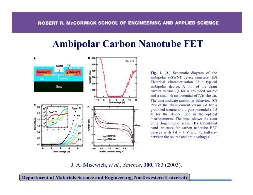
Ambipolar <strong>Carbon</strong> Nanotube FET<br />
Fig. 1. (A) Schematic diagram of the<br />
ambipolar s-SWNT device structure. (B)<br />
Electrical characterization of a typical<br />
ambipolar device. A plot of the drain<br />
current versus Vg for a grounded source<br />
and a small drain potential of1Vis shown.<br />
The data indicate ambipolar behavior. (C)<br />
Plot of the drain current versus Vd for a<br />
grounded source and a gate potential of 5<br />
V for the device used in the optical<br />
measurements. The inset shows the data<br />
on a logarithmic scale. (D) Calculated<br />
band structure for carbon nanotube FET<br />
devices with Vd = 4 V and Vg halfway<br />
between the source and drain voltages.<br />
J. A. Misewich, et al., Science, 300, 783 (2003).<br />
Department of Materials Science and Engineering, Northwestern University